Abstract
According to one embodiment, a semiconductor device includes an insulating substrate, a polycrystalline silicon semiconductor, an oxide semiconductor, a gate electrode located directly above the oxide semiconductor, a first conductive layer in contact with the polycrystalline silicon semiconductor via a first contact hole, and in contact with the oxide semiconductor via a second contact hole and a second conductive layer stacked on the first conductive layer between the first contact hole and the second contact hole. The first conductive layer includes an extending portion extending from the second contact hole toward the gate electrode. The second conductive layer is not stacked on the extending portion. The first conductive layer is thinner than the second conductive layer.
Claims (18)
1 . A semiconductor device comprising: an insulating substrate; a first insulating layer disposed above the insulating substrate; a polycrystalline silicon semiconductor disposed on the first insulating layer; an intermediate insulating layer disposed on the polycrystalline silicon semiconductor; an oxide semiconductor disposed on the intermediate insulating layer; a second insulating layer disposed on the intermediate insulating layer and the oxide semiconductor; a gate electrode disposed on the second insulating layer and located directly above the oxide semiconductor; a first conductive layer in contact with the polycrystalline silicon semiconductor via a first contact hole penetrating the intermediate insulating layer and the second insulating layer, and in contact with the oxide semiconductor via a second contact hole penetrating the second insulating layer, the second contact hole exposing the oxide semiconductor; and a second conductive layer stacked on the first conductive layer between the first contact hole and the second contact hole, wherein the first conductive layer includes an extending portion extending from the second contact hole toward the gate electrode, the second conductive layer is not stacked on the extending portion, a film thickness of the first conductive layer directly above the second insulating layer is less than a film thickness of the second conductive layer above the second insulating layer, the film thickness of the second conductive layer directly above the second insulating layer is three times or more than the film thickness of the first conductive layer above the second insulating layer, the first conductive layer is formed of a material different from that of the second conductive layer, a density of the first conductive layer is less than one half of a density of the second conductive layer, the second conductive layer includes a first end surface and a second end surface, the first end surface is located directly above the polycrystalline silicon semiconductor, and the second end surface is located directly above the oxide semiconductor.
Show 17 dependent claims
2 . The semiconductor device of claim 1 , wherein the first conductive layer contains at least one of titanium (Ti) and aluminum (Al), and the second conductive layer contains at least one of molybdenum (Mo) and tungsten (W).
3 . The semiconductor device of claim 1 , wherein the gate electrode is a stacked body comprising a first layer formed of a same material as that of the first conductive layer and a second layer formed of a same material as that of the second conductive layer.
4 . The semiconductor device of claim 1 , wherein the oxide semiconductor includes a first region directly under the gate electrode, a second region directly under the extending portion and a third region between the first region and the second region, and impurity concentrations of the second region and the third region are higher than an impurity concentration of the first region.
5 . The semiconductor device of claim 1 , wherein the second conductive layer is stacked on the first conductive layer in the second contact hole.
6 . The semiconductor device of claim 1 , wherein the second conductive layer is stacked on the first conductive layer in the first contact hole.
7 . The semiconductor device of claim 6 , wherein impurity ions contained in the polycrystalline silicon semiconductor are different in type from impurity ions contained in the oxide semiconductor.
8 . The semiconductor device of claim 1 , wherein the second conductive layer is not stacked on the first conductive layer in the first contact hole, and impurity ions contained in the polycrystalline silicon semiconductor are the same in type as impurity ions contained in the oxide semiconductor.
9 . The semiconductor device of claim 1 , wherein the second conductive layer is stacked on the first conductive layer in the first contact hole and is not stacked on the first conductive layer in the second contact hole.
10 . The semiconductor device of claim 1 , wherein the second conductive layer is stacked on the first conductive layer in the first contact hole and the second contact hole.
11 . The semiconductor device of claim 1 , wherein the second conductive layer is not stacked on the first conductive layer in the first contact hole and the second contact hole.
12 . The semiconductor device of claim 1 , wherein the intermediate insulating layer includes a third insulating layer in contact with the oxide semiconductor, and the second insulating layer and the third insulating layer are formed of silicon oxide.
13 . The semiconductor device of claim 1 , wherein the second conductive layer is not stacked on a part of the extending portion that contacts the oxide semiconductor.
14 . The semiconductor device of claim 1 , wherein the second conductive layer is not stacked on the first conductive layer over the second contact hole.
15 . The semiconductor device of claim 1 , wherein the film thickness at any portion of the second conductive layer is greater than the film thickness of the first conductive layer directly under that portion.
16 . The semiconductor device of claim 1 , wherein the oxide semiconductor includes a channel region overlapping the gate electrode, and the second insulating layer does not include a contact hole between the channel region and the gate electrode.
17 . The semiconductor device of claim 16 , wherein the second insulating layer is sandwiched between the extending portion and the oxide semiconductor, and is sandwiched between the gate electrode and the oxide semiconductor.
18 . The semiconductor device of claim 1 , wherein the second insulating layer is an inorganic insulating layer.
Full Description
Show full text →
CROSS-REFERENCE TO RELATED APPLICATIONS
This application is based upon and claims the benefit of priority from Japanese Patent Application No. 2021-009377, filed Jan. 25, 2021, the entire contents of which are incorporated herein by reference. FIELD Embodiments described herein relate generally to a semiconductor device.
BACKGROUND
For example, in the field of the liquid crystal display, such a technology has been proposed that a transistor comprising an oxide semiconductor is provided in a pixel circuit in a display area and a transistor comprising a silicon semiconductor is provided in a drive circuit in a peripheral area.
BRIEF DESCRIPTION OF THE DRAWINGS
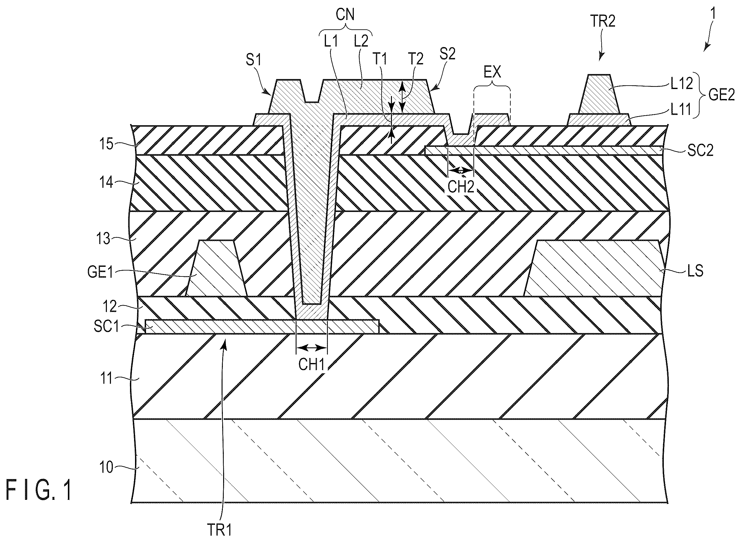
is a cross-sectional view showing a configuration example of a semiconductor device 1 according to an embodiment. is a diagram illustrating a method of manufacturing a transistor TR 1 and a transistor TR 2 . is a diagram illustrating the method of manufacturing the transistor TR 1 and the transistor TR 2 . is a diagram illustrating the method of manufacturing the transistor TR 1 and the transistor TR 2 . is a diagram illustrating the method of manufacturing the transistor TR 1 and the transistor TR 2 . is a cross-sectional view of a semiconductor SC 2 after implanting an impurity. is a diagram showing results of a first simulation. is a diagram showing results of a second simulation. is a cross-sectional view of another configuration example of the semiconductor device 1 of this embodiment. is a cross-sectional view showing another configuration example of the semiconductor device 1 of this embodiment.
DETAILED DESCRIPTION
An object to the embodiments is to provide a semiconductor device which can suppress degradation in performance of the transistor. In general, according to one embodiment, a semiconductor device comprises an insulating substrate, a first insulating layer disposed above the insulating substrate, a polycrystalline silicon semiconductor disposed on the first insulating layer, an intermediate insulating layer disposed on the polycrystalline silicon semiconductor, an oxide semiconductor disposed on the intermediate insulating layer, a second insulating layer disposed on the intermediate insulating layer and the oxide semiconductor, a gate electrode disposed on the second insulating layer and located directly above the oxide semiconductor, a first conductive layer in contact with the polycrystalline silicon semiconductor via a first contact hole penetrating the intermediate insulating layer and the second insulating layer, and in contact with the oxide semiconductor via a second contact hole penetrating the second insulating layer and a second conductive layer stacked on the first conductive layer between the first contact hole and the second contact hole, and the first conductive layer includes an extending portion extending from the second contact hole toward the gate electrode, the second conductive layer is not stacked on the extending portion, and a film thickness of the first conductive layer is less than a film thickness of the second conductive layer. Embodiments will be described hereinafter with reference to the accompanying drawings. Note that the disclosure is merely an example, and proper changes within the spirit of the invention, which are easily conceivable by a skilled person, are included in the scope of the invention as a matter of course. In addition, in some cases, in order to make the description clearer, the widths, thicknesses, shapes, etc., of the respective parts are schematically illustrated in the drawings, compared to the actual modes. However, the schematic illustration is merely an example, and adds no restrictions to the interpretation of the invention. Besides, in the specification and drawings, the same or similar elements as or to those described in connection with preceding drawings or those exhibiting similar functions are denoted by like reference numerals, and a detailed description thereof may be omitted unless otherwise necessary. A semiconductor device 1 of this embodiment is applicable to various display devices such as liquid crystal displays, organic electroluminescent displays, electrophoretic displays, and LED displays, as well as various sensors such as capacitive sensors and optical sensors, and other electronic devices. is a cross-sectional view showing a configuration example of a semiconductor device 1 of this embodiment. The semiconductor device 1 has a base 10 , insulating layers 11 to 15 , transistors TR 1 and TR 2 , and a connection electrode CN. For example, the insulating layer 11 corresponds to the first insulating layer, the insulating layers 12 to 14 correspond to an intermediate insulating layers, the insulating layer 15 corresponds to the second insulating layer, and the insulating layer 14 corresponds to the third insulating layer. The transistor TR 1 comprises a semiconductor (first semiconductor) SC 1 and a gate electrode GE 1 . The semiconductor SC 1 is, for example, a polycrystalline silicon semiconductor, but it may be some other silicon-based semiconductor. The gate electrode GE 1 is an electrode electrically connected to a gate line. The transistor TR 2 comprises a semiconductor SC 2 (second semiconductor) and a gate electrode GE 2 . The semiconductor SC 2 is, for example, an oxide semiconductor. The gate electrode GE 2 is an electrode electrically connected to a gate line. The connection electrode CN is an electrode that electrically connects the transistor TR 1 and the transistor TR 2 directly to each other. The connection electrode CN functions as either one of the source electrode or the drain electrode of the transistor TR 1 . The connection electrode CN also functions as either one of the source electrode and drain electrode of the transistor TR 2 . Note that in the transistor TR 1 , an electrode connected to an opposite side thereof to the connection electrode CN while interposing the gate electrode GE 1 therebetween (that is, the other one of the source electrode and the drain electrode) is omitted from the illustration. Further, in the transistor TR 2 , an electrode connected to an opposite side thereof to the connection electrode CN while interposing the gate electrode GE 2 therebetween (that is, the other one of the source electrode and the drain electrode) is omitted from the illustration. The base 10 is an insulating substrate and is formed of an insulating material such as glass, resin film or the like. The insulating layer 11 is disposed above the base 10 . The semiconductor SC 1 is disposed above the insulating layer 11 . The insulating layer 12 is disposed above the insulating layer 11 and covers the semiconductor SC 1 . The gate electrode GE 1 is located directly above the semiconductor SC 1 , disposed on the insulating layer 12 and covered by the insulating layer 13 . A light-shielding layer LS is provided to correspond to the transistor TR 2 , disposed on the insulating layer 12 and covered by the insulating layer 13 . In other words, the gate electrode GE 1 and the light-shielding layer LS are metal layers located in the same layer and formed of the same material. The insulating layer 14 is disposed on the insulating layer 13 . The semiconductor SC 2 is located directly above the light-shielding layer LS and disposed on the insulating layer 14 . The insulating layer 15 is disposed on the insulating layer 14 and covers the semiconductor SC 2 . In other words, in the example shown in , the insulating layers 12 to 14 , which are intermediate insulating layers, are interposed between the semiconductor SC 1 and the semiconductor SC 2 . The intermediate insulating layers are disposed on the semiconductor SC 1 and the semiconductor SC 2 is disposed on the intermediate insulating layers. The gate electrode GE 2 is located directly above the semiconductor SC 2 and is disposed on the insulating layer 15 . The gate electrode GE 2 is at the same potential as that of the light-shielding layer LS, for example. The connection electrode CN is located above the insulating layer 15 . In other words, the gate electrode GE 2 and the connection electrode CN are metal layers located in the same layer and formed of the same material. The connection electrode CN is electrically connected to the semiconductor SC 1 in a first contact hole CH 1 which penetrates the insulating layers 12 to 15 . Further, the connection electrode CN is electrically connected as well to the semiconductor SC 2 in a second contact hole CH 2 which penetrates the insulating layer 15 . The connection electrode CN is constituted by a stacked body of the first conductive layer L 1 and the second conductive layer L 2 . The second conductive layer L 2 is stacked on the first conductive layer L 1 . The first conductive layer L 1 is in contact with the semiconductor SC 1 via the first contact hole CH 1 , and also in contact with the semiconductor SC 2 via the second contact hole CH 2 . Further, the first conductive layer L 1 includes an extending portion EX which extends from a position in contact with the semiconductor SC 2 in the first contact hole CH 1 toward the gate electrode GE 2 . The second conductive layer L 2 is stacked on the first conductive layer L 1 between the first contact hole CH 1 and the second contact hole CH 2 . In the example shown in , the second conductive layer L 2 further extends to the transistor TR 1 and is stacked on the first conductive layer L 1 in the first contact hole CH 1 . The second conductive layer L 2 is not in contact with the semiconductor SC 1 in the first contact hole CH 1 . An end surface S 1 of the second conductive layer L 2 on a transistor TR 1 side is located on a gate electrode GE 1 side with respect to the position overlapping the first contact hole CH 1 . On the other hand, the second conductive layer L 2 does not extend to the transistor TR 2 and is not stacked on the first conductive layer L 1 in the second contact hole CH 2 . That is, an end surface S 2 of the second conductive layer L 2 on a transistor TR 2 side does not overlap the second contact hole CH 2 . Further, the second conductive layer L 2 is not stacked on the extending portion EX. The gate electrode GE 2 is configured as a stacked body similar to that of the connection electrode CN. That is, the gate electrode GE 2 comprises a first layer L 11 formed of the same material as that of the first conductive layer L 1 , and a second layer L 12 formed of the same material as that of the second conductive layer L 2 . The second layer L 12 is stacked on the first layer L 11 . Directly above the insulating layer 15 , a film thickness T 1 of the first conductive layer L 1 is less than a film thickness T 2 of the second conductive layer L 2 (T 1 <T 2 ). The film thickness T 2 of the second conductive layer L 2 is three times or more than the film thickness T 1 of the first conductive layer L 1 . For example, the film thickness T 1 is about 30 nm and the film thickness T 2 is T 2 is about 100 nm. The first conductive layer L 1 is formed of a material different from that of the second conductive layer L 2 . In selecting the material for each of the first and second conductive layers, it is desirable that the density of the material which forms the first conductive layer L 1 is lower than the density of the material which forms the second conductive layer L 2 . For example, the material of the first conductive layer L 1 contains at least one of titanium (Ti) and aluminum (Al), and the material of the second conductive layer L 2 contains at least one of molybdenum (Mo) and tungsten (W). However, since the first conductive layer L 1 is in contact with the semiconductor SC 2 , which is an oxide semiconductor, it is desirable that it be formed of a material that is not easily oxidized. For example, the first conductive layer L 1 should preferably be a single layer of titanium-based material or a stacked body in which an aluminum-based layer is stacked on a titanium-based layer. The insulating layers 11 to 15 are, for example, transparent inorganic insulating layers formed of silicon nitride (SiN), silicon oxide (SiO) and the like. The insulating layers 11 to 15 may each be a single layer formed of a single insulating material or may be a stacked body formed from multiple insulating materials. For example, the insulating layer 11 is a stacked body of a silicon nitride and a silicon oxide, the insulating layer 12 is formed of silicon oxide, the insulating layer 13 is formed of silicon nitride, and the insulating layers 14 and 15 are formed of silicon oxide. Next, an example of a method of manufacturing the transistors TR 1 and TR 2 shown in will be described. to 5 illustrate the method of manufacturing the transistors TR 1 and TR 2 . In the cross-sectional views shown in to 5 , the base 10 is omitted from the illustration. First, as shown in , the insulating layer 11 , the semiconductor (polycrystalline silicon semiconductor) SC 1 , the insulating layer 12 , the gate electrode GE 1 , the light-shielding layer LS, the insulating layers 13 and 14 , the semiconductor (oxide semiconductor) SC 2 and the insulating layer 15 are formed in order. Note that, before forming the semiconductor SC 2 , an impurity is implanted to the semiconductor SC 1 using the gate electrode GE 1 as a mask. Here, the impurity implanted is, for example, phosphorus (P) in the case of n-channel type, whereas boron (B) in the case of p-channel type. After forming insulating layer 15 , the first contact hole CH 1 which penetrates the insulating layers 12 to 15 to the semiconductor SC 1 , and the second contact hole CH 2 which penetrates the insulating layer 15 to the semiconductor SC 2 are formed. In the first contact hole CH 1 , a part of the semiconductor SC 1 is exposed, and in the second contact hole CH 2 , a part of the semiconductor SC 2 is exposed. Then, as shown in , a metal film is formed on the insulating layer 15 , and the metal film is patterned, thus forming the first conductive layer L 1 of the connection electrode CN and the first layer L 11 of the gate electrode GE 2 . The first conductive layer L 1 is in contact with the semiconductor SC 1 in the first contact hole CH 1 , and in contact with the semiconductor SC 2 in the second contact hole CH 2 , and further includes an extending portion EX. The first layer L 11 is located directly above the semiconductor SC 2 and is spaced apart from the first conductive layer L 1 . In the region of the semiconductor SC 2 , which is in contact with the first conductive layer L 1 , oxygen is absorbed by the first conductive layer L 1 , thus lowering the resistance. Next, as shown in , after forming a metal film, the metal film is patterned, thus forming the second conductive layer L 2 of the connection electrode CN and the second layer L 12 of the gate electrode GE 2 . The second conductive layer L 2 overlaps the first conductive layer L 1 in the first contact hole CH 1 , and further overlaps the first conductive layer L 1 between the first contact hole CH 1 and the second contact hole CH 2 . The second layer L 12 overlaps the first layer L 11 and is spaced apart from the second conductive layer L 2 . Subsequently, as shown in , ion implantation is carried out on the semiconductor SC 2 using the gate electrode GE 2 as a mask. For example, boron (B) is implanted to the semiconductor SC 2 as the impurity by the ion implantation. In place of boron, some other impurity such as phosphorus (P) may be implanted to the semiconductor SC 2 . In such ion implantation, the second conductive layer L 2 and the second layer L 12 , which have relatively high-density and is relatively thick, have a high ability to block the implantation of impurities. Therefore, in the region directly under the gate electrode GE 2 , which is a stacked body of the first layer L 11 and the second layer L 12 , substantially no impurities are implanted. On the other hand, impurities are implanted to the region directly under the first conductive layer L 1 , which is thin and the region where the insulating layer 15 is exposed. Especially, the first conductive layer L 1 is formed of a relatively low-density material, and therefore, impurities easily permeate therethrough. With this configuration, impurities can be easily implanted to, for example, the region directly below the extending portion EX, including the region where the insulating layer 15 is covered only by the first conductive layer L 1 . Therefore, in the semiconductor SC 2 , impurities are implanted to the region directly under the extending portion EX and the region between the first conductive layer L 1 and the gate electrode GE 2 , and thus the resistance of these regions are lowered. Incidentally, as described above, when the transistor TR 1 is of an n-channel type, the impurity to be implanted to the semiconductor SC 1 is phosphorus. Here, when boron is to be implanted as an impurity to the semiconductor SC 2 , the impurity contained in the semiconductor SC 1 is different in type from that of the semiconductor SC 2 . Therefore, when implanting an impurity to the semiconductor SC 2 , it is necessary to protect the semiconductor SC 1 from being implanted with the impurity (boron). Thus, in the first contact hole CH, the second conductive layer L 2 is stacked on the first conductive layer L 1 . Further, as in the case where the semiconductor SC 1 of the p-channel transistor TR 1 contains boron as an impurity and phosphorus is to be implanted as an impurity to the semiconductor SC 2 , for the purpose of suppressing undesired impurities from being implanted to the semiconductor SC 2 , the second conductive layer L 2 is stacked on the first conductive layer L 1 in the first contact hole CH 1 . In the case where the impurity contained in the semiconductor SC 1 is the same in type as that of the semiconductor SC 2 , the second conductive layer L 2 of the first contact hole CH 1 may be omitted. For example, in the case where the impurity contained in the semiconductor SC 1 is phosphorus and phosphorus is to be implanted as an impurity to the semiconductor SC 2 , or the case where the impurity contained in the semiconductor SC 1 is boron and boron is to be implanted as an impurity to the semiconductor SC 2 , the second conductive layer L 2 of the first contact hole CH 1 may be omitted. is a cross-sectional view showing the semiconductor SC 2 after implanting the impurity. The semiconductor SC 2 includes regions A 1 to A 5 . Each of these regions will now be described in detail. The region (first region) A 1 is located directly under the gate electrode GE 2 . The region (second region) A 2 is located directly under the extending portion EX. The region (third region) A 3 is located between the region A 1 and the region A 2 and is connected to the regions A 1 and A 2 . The region A 4 is located on an opposite side to the region A 3 while interposing the region A 1 therebetween. In other words, the region A 1 is located between the region A 3 and the region A 4 , and is connected to the regions A 3 and A 4 . The region A 3 and the region A 4 overlap the region of the insulating layer 15 , which is exposed from the first conductive layer L 11 and the first layer L 11 . The region A 5 is a region in contact with the first conductive layer L 1 in the second contact hole CH 2 . The impurity concentration of each of the regions A 2 to A 5 is higher than that of the region A 1 . Note that the impurity concentrations of the regions A 2 to A 5 are substantially equal to each other. For example, boron (B) is implanted as an impurity in each of the regions A 2 to A 5 , whereas in the region A 1 , boron (B) is no substantially implanted. That is, the region A 1 corresponds to the channel region of the semiconductor SC 2 . The impurity concentration in this specification can be expressed as the number of impurity ions (atoms) per unit volume. Note that as to oxide semiconductors, a high impurity concentration means a large number of oxygen defects per unit volume or a large number of defects per unit volume. From another point of view, in the semiconductor SC 2 , the regions A 2 to A 5 each have a resistance lower than that of the region A 1 . The resistance values of the regions A 2 to A 4 are substantially equal to each other. The region A 5 is in contact with the first conductive layer L 1 , and has a resistance even lower than that of the region A 2 . Next, the impurity concentrations in portions P 1 and P 2 encircled by dotted lines in the cross-sectional view shown in were calculated by simulation. In this simulation, the concentration of boron was calculated as the impurity concentration. The portion P 1 is a region where the extending portion EX of the first conductive layer L 1 , the insulating layer 15 , the region A 2 of the semiconductor SC 2 and the insulating layer 14 are stacked. The portion P 2 is a region where the first conductive layer L 1 is not formed and further the insulating layer 15 , the region A 3 of the semiconductor SC 2 and the insulating layer 14 are stacked. is a diagram showing results of the first simulation. Here, the acceleration energy at the time of the ion implantation is set to 30 keV, and the ion dosage is set to 1×10 15 ions/cm 2 . The horizontal axis of the figure indicates the distance (nm) in the depth direction with respect to the interface between the insulating layer 15 and the semiconductor SC 2 . As to the position in the depth direction, the left direction of the graph corresponds to the upper direction of the portions P 1 and P 2 , and the right direction of the graph corresponds to the lower direction of the portions P 1 and P 2 . In the upper part of the graph, the range of the extending portion EX is represented by “EX”, the range of the insulating layer 15 is represented by “ 15 ”, the range of the semiconductor SC 2 is represented by “SC 2 ”, and the range of the insulating layer 14 is represented by “ 14 ”. The film thickness of the extending portion EX is about 30 nm, the film thickness of the insulating layer 15 is about 100 nm, and the film thickness of the semiconductor SC 2 is about 50 nm. The vertical axis of the figure indicates the concentration of the boron impurity (atoms/cm 3 ). The diagram shows the simulation results B 1 of the portion P 1 and the simulation results B 2 of the portion P 2 . According to the results of the first simulation shown in , the impurity concentration of the semiconductor SC 2 (the region A 2 ) in the portion P 1 is lower than that of the semiconductor SC 2 (the region A 3 ) in the portion P 2 ; however, it has been confirmed that impurities of a concentration sufficient to lower the resistance of the region A 2 located directly under the extending portion EX can be implanted to the region A 2 . is a diagram showing results of the second simulation. Here, the acceleration energy at the time of the ion implantation is set to 50 keV, and the ion dosage is set to 1×10 15 ions/cm 2 . The diagram shows the simulation results B 1 of the portion P 1 and the simulation results B 2 of the portion P 2 . According to the results of the second simulation shown in , the impurity concentration of the semiconductor SC 2 (the region A 2 ) in the portion P 1 is higher than that of the semiconductor SC 2 (the region A 3 ) in the portion P 2 . In the results of the second simulation as well, it has been confirmed that impurities of a concentration sufficient to lower the resistance of the region A 2 located directly under the extending portion EX can be implanted to the region A 2 . It has been also confirmed that the balance of impurity concentration in the regions of the semiconductor SC 2 can be adjusted by adjusting the acceleration energy. As described above, the connection electrode CN, which electrically connects the semiconductor SC 1 , which is a polycrystalline silicon semiconductor and the semiconductor SC 2 , which is an oxide semiconductor, directly to each other, is configured as a stacked body of the first conductive layer L 1 which is thin and the second conductive layer L 2 which is thick. Note that the second conductive layer L 2 is not provided in a region on a gate electrode GE 2 side with respect to the second contact hole CH 2 where the first conductive layer L 1 and the semiconductor SC 2 are in contact with each other. When a thick-film connection electrode CN is formed, the extending portion EX located on the gate electrode GE 2 side with respect to the second contact hole CH 2 serves as an eaves, which may interfere with the implantation of an impurity to the region A 2 directly below the extending portion EX when the ion implantation is carried out on the semiconductor SC 2 . In this case, the resistance of the region A 2 is not sufficiently lowered and the desired performance of the transistor TR 2 cannot be obtained. According to this embodiment described above, when ion implantation is carried out on the semiconductor SC 2 , the impurity is implanted to the regions A 2 and A 3 between the contact position between the first conductive layer L 1 and the semiconductor SC 2 and the region A 1 which is the channel region, and the resistances of the regions A 2 and A 3 can be lowered. Thus, a transistor TR 2 with the desired performance can be provided. Further, in the first contact hole CH 1 , where the first conductive layer L 1 and the semiconductor SC 1 come into contact with each other, the second conductive layer L 2 is provided. Therefore, even if the impurity implanted to the semiconductor SC 1 and that implanted to the semiconductor SC 2 are different from each other in type, the implantation of different impurities to the semiconductor SC 1 can be suppressed. With this configuration, the increase in the contact resistance between the semiconductor SC 1 and the connection electrode CN can be suppressed. Therefore, the decrease in the drive capability of the transistor TR 1 can be suppressed. Furthermore, it is not necessary to provide a separate processing step for suppressing undesired impurity implantation to the semiconductor SC 1 , and the increase in manufacturing cost can be suppressed. is a cross-sectional view showing another configuration example of the semiconductor device 1 of this embodiment. The configuration example shown in is different from that of in the second conductive layer L 2 . Note that the first conductive layer L 1 is, as in the case of the configuration example of , in contact with the semiconductor SC 1 via the first contact hole CH 1 and also in contact with the semiconductor SC 2 via the second contact hole CH 2 . Further, the first conductive layer L 1 includes an extending portion EX extending from a position in contact with the semiconductor SC 2 in the first contact hole CH 1 towards the gate electrode GE 2 . The second conductive layer L 2 is stacked on the first conductive layer L 1 between the first contact hole CH 1 and the second contact hole CH 2 , and stacked on the first conductive layer L 1 in the first contact hole CH 1 and further stacked on the first conductive layer L 1 in the second contact hole CH 2 . Note that the second conductive layer L 2 is not stacked on the extending portion EX. In other words, the end surface S 2 of the second conductive layer L 2 on the transistor TR 2 side overlaps the second contact hole CH 2 . In the example with such a configuration, impurity implantation to the region A 5 in the semiconductor SC 2 , which overlaps the second contact hole CH 2 , is suppressed. The region A 5 is in contact with the connection electrode CN, therefore the oxygen in the region A 5 is absorbed by the connection electrode CN, and therefore the resistance of the region A 5 is sufficiently lowered. In the example with such a configuration as well, the second conductive layer L 2 is not stacked on the extending portion EX, and therefore advantageous effects similar to those of the configuration examples provided above can be obtained. is a cross-sectional view showing another configuration example of the semiconductor device 1 of this embodiment. The configuration example shown in is different from that of in the second conductive layer L 2 . More specifically, the second conductive layer L 2 is stacked on the first conductive layer L 1 between the first contact hole CH 1 and the second contact hole CH 2 . On the other hand, the second conductive layer L 2 is not extended to the transistor TR 1 , and the second conductive layer L 2 is not stacked on the first conductive layer L 1 in the first contact hole CH 1 . In other words, the end surface S 1 of the second conductive layer L 2 on the transistor TR 1 side does not overlap the first contact hole CH 1 . Further, the second conductive layer L 2 is not stacked on the first conductive layer L 1 in the second contact hole CH 2 , and also not stacked on the extending portion EX. In the example with such a configuration, the impurity contained in the semiconductor SC 1 is the same in type as that contained in the semiconductor SC 2 . Therefore, even if the same type of impurity as that of the semiconductor SC 2 is implanted to the semiconductor SC 1 while implanting the impurity to the semiconductor SC 2 , the performance of the transistor TR 1 is not deteriorated. In the example with such a configuration as well, the second conductive layer L 2 is not stacked on the extending portion EX, and therefore advantageous effects similar to those of the configuration examples provided above can be obtained. According to the embodiments, it is possible to provide a semiconductor device which can suppress the degradation in performance of the transistor. Based on the semiconductor device which has been described in the above-described embodiments, a person having ordinary skill in the art may achieve a semiconductor device with an arbitral design change; however, as long as they fall within the scope and spirit of the present invention, such a semiconductor device is encompassed by the scope of the present invention. A skilled person would conceive various changes and modifications of the present invention within the scope of the technical concept of the invention, and naturally, such changes and modifications are encompassed by the scope of the present invention. For example, if a skilled person adds/deletes/alters a structural element or design to/from/in the above-described embodiments, or adds/deletes/alters a step or a condition to/from/in the above-described embodiment, as long as they fall within the scope and spirit of the present invention, such addition, deletion, and altercation are encompassed by the scope of the present invention. Furthermore, regarding the present embodiments, any advantage and effect those will be obvious from the description of the specification or arbitrarily conceived by a skilled person are naturally considered achievable by the present invention.
Figures (8)
Citations
This patent cites (8)
- US2006/0255345
- US2009/0026450
- US2017/0278872
- US2020/0259020
- US2021/0241689
- US110323230
- US2017-183312
- US2020-129635