Abstract
A semiconductor device includes a first semiconductor chip in which a first multilayer wiring structure including a first coil and a second coil is formed and a second semiconductor chip in which a second multilayer wiring structure including a third coil and a fourth coil is formed. The second semiconductor chip is joined to the first semiconductor chip such that the first coil (second coil) and the third coil (fourth coil) are overlapped and the second semiconductor chip does not have an offset structure with respect to the first semiconductor chip. The second semiconductor chip is joined to the first semiconductor chip such that it is not overlapped with a pad for the first semiconductor chip and a pad for the second semiconductor chip.
Claims (9)
1 . A semiconductor device comprising a first semiconductor chip and a second semiconductor chip, in which a first semiconductor circuit and a second semiconductor circuit are formed, wherein the first semiconductor chip includes: a first semiconductor substrate having a first main surface; and a first multilayer wiring structure which is formed on the first semiconductor substrate so as to cover the first main surface and in which a plurality of conductive films and a plurality of insulating films are stacked, wherein the second semiconductor chip includes: a second semiconductor substrate having a second main surface; and a second multilayer wiring structure which is formed on the second semiconductor substrate so as to cover the second main surface, wherein the second semiconductor circuit includes a first portion of the second semiconductor circuit and a second portion of the second semiconductor circuit, wherein the first semiconductor circuit and the first portion of the second semiconductor circuit are formed in the first semiconductor chip, wherein the second portion of the second semiconductor circuit electrically connected to the first portion of the second semiconductor circuit is formed in the second semiconductor chip, wherein the first multilayer wiring structure includes: a first inductor electrically connected to the first semiconductor circuit; a first electrode portion electrically connected to the first semiconductor circuit; and a second electrode portion electrically connected to the first portion of the second semiconductor circuit, wherein the second multilayer wiring structure includes a second inductor electrically connected to the second portion of the second semiconductor circuit, wherein the first multilayer wiring structure and the second multilayer wiring structure are joined such that the first inductor and the second inductor are overlapped in plan view showing the first main surface of the first semiconductor substrate, wherein the second semiconductor chip is joined to the first semiconductor chip such that the second semiconductor chip does not protrude from the first semiconductor chip and is not overlapped with the first electrode portion and the second electrode portion in plan view showing the first main surface of the first semiconductor substrate, wherein the first multilayer wiring structure includes at least three first dummy electrode portions which are not arranged in a straight line, wherein the second multilayer wiring structure includes at least three second dummy electrode portions which are not arranged in a straight line, wherein the at least three first dummy electrode portions and the at least three second dummy electrode portions are overlapped in plan view showing the first main surface of the first semiconductor substrate, wherein a second conductive member is interposed each between the at least three first dummy electrode portions and the at least three second dummy electrode portions, wherein, in the first semiconductor chip: the first semiconductor circuit is operated by a first voltage; the first portion of the second semiconductor circuit is operated by a second voltage lower than the first voltage; the first semiconductor circuit, the first electrode portion and the first inductor are formed in a first region defined on the first main surface of the first semiconductor substrate; and the first portion of the second semiconductor circuit, the second electrode portion and the at least three second dummy electrode portions are formed in a second region defined on the first main surface of the first semiconductor substrate, and wherein an isolation insulating film is formed between the first region and the second region.
Show 8 dependent claims
2 . The semiconductor device according to claim 1 , wherein the first multilayer wiring structure includes a third electrode portion electrically connected to the first portion of the second semiconductor circuit, wherein the second multilayer wiring structure includes a fourth electrode portion electrically connected to the second portion of the second semiconductor circuit and electrically connected to the third electrode portion, wherein the third electrode portion and the fourth electrode portion are overlapped in plan view showing the first main surface of the first semiconductor substrate, and wherein a first conductive member is interposed between the third electrode portion and the fourth electrode portion.
3 . The semiconductor device according to claim 1 , wherein a noise blocking portion configured to block propagation of an electrical noise generated in the first semiconductor circuit to which the first voltage is supplied, to the first portion of the second semiconductor circuit is formed between the first region and the second region in the first semiconductor substrate.
4 . The semiconductor device according to claim 3 , wherein the noise blocking portion includes: an insulator formed from the first main surface of the first semiconductor substrate to a predetermined depth; and a second conductivity type region formed from the insulator to the second region of the first semiconductor substrate, in the first semiconductor substrate of a first conductivity type.
5 . The semiconductor device according to claim 1 , wherein the plurality of conductive films include an uppermost conductive film farthest from the first main surface of the first semiconductor substrate, and wherein a recess portion is formed at least in a portion of one insulating film of the plurality of insulating films, on which the uppermost conductive film is formed, the portion being located between the first region and the second region.
6 . The semiconductor device according to claim 5 , wherein the uppermost conductive film includes an aluminum film, and wherein the recess portion is formed from an upper surface of the one insulating film in contact with a lower surface of the uppermost conductive film to a side on which the first main surface is located.
7 . The semiconductor device according to claim 5 , wherein the uppermost conductive film includes a copper film, and wherein the recess portion is formed from an upper surface of the one insulating film located at the same height as an upper surface of the uppermost conductive film to a side on which the first main surface is located.
8 . The semiconductor device according to claim 5 , wherein the uppermost conductive film includes the first electrode portion and the second electrode portion.
9 . The semiconductor device according to claim 8 , wherein the uppermost conductive film includes the first inductor.
Full Description
Show full text →
CROSS-REFERENCE TO RELATED APPLICATIONS
The disclosure of Japanese Patent Application No. 2021-143219 filed on Sep. 2, 2021 including the specification, drawings and abstract is incorporated herein by reference in its entirety.
BACKGROUND
The present invention relates to a semiconductor device, and can be suitably applied to, for example, a semiconductor device having a digital isolator. In recent years, in the field of automobiles, the conversion of power source from gasoline engines to motors has been attempted in order to protect the environment. The rotation speed of the motor is controlled by a power semiconductor device equipped with a power semiconductor element for electric power. The power semiconductor device is controlled by a semiconductor device provided with a microcomputer. A semiconductor device equipped with a power semiconductor element for electric power handles a voltage of about several hundred volts (V) to one thousand and several hundred volts (V). On the other hand, a semiconductor device equipped with a microcomputer is driven by a voltage of about several volts (V). For the control of the semiconductor device equipped with the power semiconductor element for electric power by the microcomputer, a digital isolator is applied in order to transmit and receive an electric signal between a circuit including the power semiconductor element and a circuit including the microcomputer. In the digital isolator, an electric signal is transmitted by using the electromagnetic induction between an inductor (one inductor) electrically connected to the circuit including the power semiconductor element and an inductor (the other inductor) electrically connected to the circuit including the microcomputer. There are disclosed techniques listed below. [Patent Document 1] Japanese Unexamined Patent Application Publication No. 2016-127162 As a structure for transmitting the electric signal, for example, a structure (semiconductor device) in which one semiconductor chip in which one inductor is formed and the other semiconductor chip in which the other inductor is formed are joined is proposed in Patent Document 1. In this semiconductor device, the surface of one semiconductor chip and the surface of the other semiconductor chip are joined by a tape-shaped insulating material in the state where one inductor and the other inductor face each other.
SUMMARY
Further miniaturization has been required for the semiconductor device provided with a digital isolator. Other objects and novel features will be apparent from the description of this specification and accompanying drawings. A semiconductor device according to an embodiment has a first semiconductor chip and a second semiconductor chip, in which a first semiconductor circuit and a second semiconductor circuit are formed. The first semiconductor chip includes a first semiconductor substrate and a first multilayer wiring structure. The first semiconductor substrate has a first main surface. The first multilayer wiring structure is formed on the first semiconductor substrate so as to cover the first main surface, and a plurality of conductive films and a plurality of insulating films are stacked in the first multilayer wiring structure. The second semiconductor chip includes a second semiconductor substrate and a second multilayer wiring structure. The second semiconductor substrate has a second main surface. The second multilayer wiring structure is formed on the second semiconductor substrate so as to cover the second main surface. The second semiconductor circuit includes a first portion of the second semiconductor circuit and a second portion of the second semiconductor circuit. The first semiconductor circuit and the first portion of the second semiconductor circuit are formed in the first semiconductor chip. The second portion of the second semiconductor circuit electrically connected to the first portion of the second semiconductor circuit is formed in the second semiconductor chip. The first multilayer wiring structure includes a first inductor, a first electrode portion, and a second electrode portion. The first inductor is electrically connected to the first semiconductor circuit. The first electrode portion is electrically connected to the first semiconductor circuit. The second electrode portion is electrically connected to the first portion of the second semiconductor circuit. The second multilayer wiring structure includes a second inductor electrically connected to the second portion of the second semiconductor circuit. The first multilayer wiring structure and the second multilayer wiring structure are joined such that the first inductor and the second inductor are overlapped in plan view showing the first main surface of the first semiconductor substrate. The second semiconductor chip is joined to the first semiconductor chip such that the second semiconductor chip does not protrude from the first semiconductor chip and is not overlapped with the first electrode portion and the second electrode portion in plan view showing the first main surface of the first semiconductor substrate. With the semiconductor device according to the embodiment described above, it is possible to contribute to further miniaturization of the semiconductor device.
BRIEF DESCRIPTION OF THE DRAWINGS
is a circuit diagram showing an example of a circuit of a semiconductor device according to each embodiment. is a plan view showing an example of an external appearance of the semiconductor device according to each embodiment. is a cross-sectional view taken along the cross-sectional line III-III shown in in each embodiment. is a plan view showing an example of a structure of a first semiconductor chip in the semiconductor device according to the first embodiment. is a plan view showing an example of a structure of a second semiconductor chip in the semiconductor device in the first embodiment. is a plan view showing an example of a structure in the state where the second semiconductor chip is joined to the first semiconductor chip in the first embodiment. is a cross-sectional view taken along the cross-sectional line VII-VII shown in in the first embodiment. is a cross-sectional view taken along the cross-sectional line VIII-VIII shown in in the first embodiment. is a plan view showing a step of a method of manufacturing the first semiconductor chip in a method of manufacturing the semiconductor device in the first embodiment. is a cross-sectional view taken along the cross-sectional line X-X shown in in the first embodiment. is a cross-sectional view taken along the cross-sectional line XI-XI shown in in the first embodiment. is a plan view showing a step of a method of manufacturing the second semiconductor chip in the method of manufacturing the semiconductor device in the first embodiment. is a cross-sectional view taken along the cross-sectional line XIII-XIII shown in in the first embodiment. is a cross-sectional view taken along the cross-sectional line XIV-XIV shown in in the first embodiment. is a first cross-sectional view showing a step performed after the steps shown in and in the first embodiment. is a second cross-sectional view in the step shown in in the first embodiment. is a cross-sectional view of a semiconductor device according to a comparative example. is a plan view showing an example of a structure of a semiconductor device according to the second embodiment. is a cross-sectional view taken along the cross-sectional line XIX-XIX shown in in the second embodiment. is a cross-sectional view taken along the cross-sectional line XX-XX shown in in the second embodiment. is a plan view showing a structure of a first example and a second example of a semiconductor device according to the third embodiment. is a cross-sectional view of the semiconductor device according to the first example taken along the cross-sectional line XXII-XXII shown in in the third embodiment. is a cross-sectional view of the semiconductor device according to the first example taken along the cross-sectional line XXIII-XXIII shown in in the third embodiment. is a cross-sectional view of the semiconductor device according to the second example taken along the cross-sectional line XXII-XXII shown in in the third embodiment. is a cross-sectional view of the semiconductor device according to the second example taken along the cross-sectional line XXIII-XXIII shown in in the third embodiment. is a partial plan view showing an example of a variation of a pattern of a recess portion formed in the semiconductor device in the third embodiment. is a partial plan view showing another example of the variation of the pattern of the recess portion formed in the semiconductor device in the third embodiment.
DETAILED DESCRIPTION
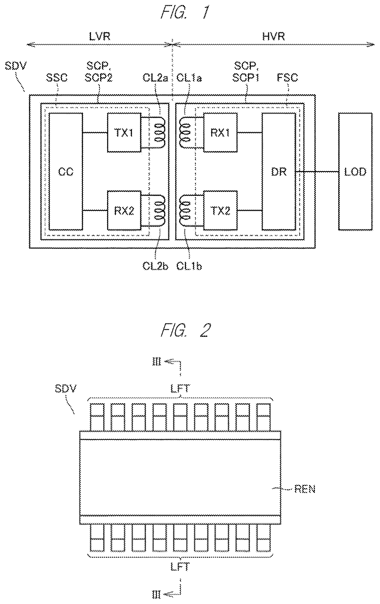
First, an example of a circuit of a semiconductor device provided with a digital isolator and an outline of a structure thereof according to each embodiment will be described. As shown in , a semiconductor device SDV includes a first semiconductor chip SCP 1 and a second semiconductor chip SCP 2 . A circuit FSC for the first semiconductor chip including a semiconductor element or the like for driving a load LOD such as a motor is formed in the first semiconductor chip SCP 1 . A circuit SSC for the second semiconductor chip including a semiconductor element or the like for driving a load LOD is formed in the second semiconductor chip SCP 2 . As will be described later, a part of the circuit SSC for the second semiconductor chip is formed in the first semiconductor chip SCP 1 . The circuit FSC for the first semiconductor chip includes a drive circuit DR, a receiver circuit RX 1 , and a transmission circuit TX 1 . The drive circuit DR is electrically connected to the load LOD. The receiver circuit RX 1 and the transmission circuit TX 1 are electrically connected to the drive circuit DR. A coil CL 1 a is electrically connected to the receiver circuit RX 1 . A coil CL 1 b is electrically connected to the transmission circuit TX 1 . The circuit FSC for the first semiconductor chip operates (drives) at about several hundred volts (V) to one thousand and several hundred volts (V). The circuit FSC for the first semiconductor chip is formed in a high voltage region HVR in the semiconductor device SDV. The circuit SSC for the second semiconductor chip includes a control circuit CC, a receiver circuit RX 2 , and a transmission circuit TX 2 . The receiver circuit RX 2 and the transmission circuit TX 2 are electrically connected to the control circuit CC. A coil CL 2 a is electrically connected to the transmission circuit TX 2 . A coil CL 2 b is electrically connected to the receiver circuit RX 2 . The circuit SSC for the second semiconductor chip operates (drives) at about several volts (V). The circuit SSC for the second semiconductor chip is formed in a low voltage region LVR in the semiconductor device SDV. The coil CL 1 a and the coil CL 2 a are arranged so as to face each other. The coil CL 1 a and the coil CL 2 a are magnetically coupled to each other. The coil CL 1 b and the coil CL 2 b are arranged so as to face each other. The coil CL 1 b and the coil CL 2 b are magnetically coupled to each other. A signal is transmitted from the control circuit CC to the transmission circuit TX 1 . The signal transmitted to the transmission circuit TX 1 flows through the coil CL 2 a as a current. When a current flows through the coil CL 2 a , an induced current flows through the coil CL 1 a by electromagnetic induction. The induced current flowing through the coil CL 1 a is transmitted as a signal to the drive circuit DR via the receiver circuit RX 1 . In this way, the signal of the control circuit CC is transmitted to the drive circuit DRC. On the other hand, a signal is transmitted from the drive circuit DR to the transmission circuit TX 2 . The signal transmitted to the transmission circuit TX 2 flows through the coil CL 1 b as a current. When a current flows through the coil CL 1 b , an induced current flows through the coil CL 2 b by electromagnetic induction. The induced current flowing through the coil CL 2 b is transmitted as a signal to the control circuit CC via the receiver circuit RX 2 . In this way, the signal of the drive circuit DR is transmitted to the control circuit CC. By the series of operations above, the drive of the load LOD is controlled. Next, an example of an overall structure of the semiconductor device SDV will be described. As shown in and , in the semiconductor device SDV, a semiconductor chip SCP is mounted on a lead frame LFM. The semiconductor chip SCP mounted on the lead frame LFM is sealed by sealing resin REN. Lead terminals LFT are exposed from the sealing resin REN. As the sealing resin REN, for example, an epoxy resin is used. The semiconductor chip SCP includes the first semiconductor chip SCP 1 and the second semiconductor chip SCP 2 . The second semiconductor chip SCP 2 is connected (bonded) on the first semiconductor chip SCP 1 . The first semiconductor chip SCP 1 and the second semiconductor chip SCP 2 are electrically connected by flip-chip connection. The first semiconductor chip SCP 1 and the lead terminal LFT (lead frame LFM) are electrically connected by a wire WIR 1 and a wire WIR 2 . Hereinafter, the structure of the semiconductor device SDV will be described more specifically. First Embodiment An example of the semiconductor device according to the first embodiment will be described. As described above, the semiconductor device SDV includes the first semiconductor chip SCP 1 and the second semiconductor chip SCP 2 as the semiconductor chip SCP. The circuit FSC for the first semiconductor chip (first semiconductor circuit) and the circuit SSC for the second semiconductor chip (second semiconductor circuit) are formed in the semiconductor device SDV. The circuit SSC for the second semiconductor chip includes a first circuit portion SSC 1 for the second semiconductor chip (first portion of second semiconductor circuit) and a second circuit portion SSC 2 for the second semiconductor chip (second portion of second semiconductor circuit). First, the first semiconductor chip SCP 1 will be described. As shown in , the circuit FSC for the first semiconductor chip that drives the load LOD such as a motor is formed in the first semiconductor chip SCP 1 . Further, the first circuit portion SSC 1 for the second semiconductor chip of the circuit SSC for the second semiconductor chip is formed in the first semiconductor chip SCP 1 . A pad FPDF (first electrode portion) for the first semiconductor chip is arranged on a first main surface side of the first semiconductor substrate SUB 1 in the first semiconductor chip SCP 1 . The pad FPDF for the first semiconductor chip is electrically connected to the circuit FSC for the first semiconductor chip. The pad FPDF for the first semiconductor chip is electrically connected to the lead frame LFM by the wire WIR 1 (see ). Further, the coil CL 1 a and the coil CL 1 b (first inductor) are arranged on the first main surface side of the first semiconductor substrate SUB 1 . The coil CL 1 a and the coil CL 1 b are electrically connected to the circuit FSC for the first semiconductor chip. The coil CL 1 a and the coil CL 1 b face the coil CL 2 a and the coil CL 2 b (see ) in the second semiconductor chip SCP 2 . Further, a pad FPDS (second electrode portion) for the second semiconductor chip and a pad FPDC (third electrode portion) for connecting the second semiconductor chip to be electrically connected to the second semiconductor chip SCP 2 are arranged on the first main surface side of the first semiconductor substrate SUB 1 . The pad FPDS for the second semiconductor chip functions as a silicon interposer of the second semiconductor chip SCP 2 . The pad FPDS for the second semiconductor chip is electrically connected to the lead frame LFM by the wire WIR 2 . The pad FPDS for the second semiconductor chip is arranged in a region outside the region where the second semiconductor chip SCP 2 is arranged, on the first main surface side of the first semiconductor substrate SUB 1 . The first circuit portion SSC 1 for the second semiconductor chip includes an uppermost conductive film MAU (see ) that electrically connects the pad FPDS for the second semiconductor chip and the pad FPDC for connecting the second semiconductor chip. The pad FPDC for connecting the second semiconductor chip is arranged in a region in which the second semiconductor chip SCP 2 is arranged, on the first main surface side of the first semiconductor substrate SUB 1 . The pad FPDC for connecting the second semiconductor chip is to be electrically connected to a pad SPDC for connecting the first semiconductor chip (see ) in the second semiconductor chip SCP 2 . Further, a plurality of dummy pads FDP are arranged on the first main surface side of the first semiconductor substrate SUB 1 . The plurality of dummy pads FDP are arranged in the region to which the second semiconductor chip SCP 2 is joined. The plurality of dummy pads FDP include at least three dummy pads FDP that are not arranged in a straight line. Next, the second semiconductor chip SCP 2 will be described. As shown in , the second circuit portion SSC 2 for the second semiconductor chip of the circuit SSC for the second semiconductor chip is formed in the second semiconductor chip SCP 2 . The second circuit portion SSC 2 for the second semiconductor chip substantially controls the drive of the load LOD. The pad SPDC (fourth electrode portion) for connecting the first semiconductor chip is arranged on the second main surface side of the second semiconductor substrate SUB 2 in the second semiconductor chip SCP 2 . The pad SPDC for connecting the first semiconductor chip is to be electrically connected to the pad FPDC for connecting the second semiconductor chip in the first semiconductor chip SCP 1 . Also, the coil CL 2 a and the coil CL 2 b (second inductor) are arranged on the second main surface side of the second semiconductor substrate SUB 2 in the second semiconductor chip SCP 2 . The coil CL 2 a and the coil CL 2 b are electrically connected to the second circuit portion SSC 2 for the second semiconductor chip. The coil CL 2 a and the coil CL 2 b face the coil CL 1 a and the coil CL 1 b (see ) in the first semiconductor chip SCP 1 . Further, a plurality of dummy pads SDP are arranged on the second main surface side of the second semiconductor substrate SUB 2 . The plurality of dummy pads SDP include at least three dummy pads SDP that are not arranged in a straight line. Each of the plurality of dummy pads SDP faces the corresponding dummy pad FDP of the plurality of dummy pads FDP formed in the first semiconductor chip SCP 1 . Next, the state in which the second semiconductor chip SCP 2 is mounted on the first semiconductor chip SCP 1 will be described. As shown in , , and , a first multilayer wiring structure ML 1 is formed in the first semiconductor chip SCP 1 so as to cover the first main surface of the first semiconductor substrate SUB 1 . A plurality of conductive films and a plurality of insulating films are stacked in the first multilayer wiring structure ML 1 . A second multilayer wiring structure ML 2 is formed in the second semiconductor chip SCP 2 so as to cover the second main surface of the second semiconductor substrate SUB 2 . In the semiconductor device SDV, the first multilayer wiring structure ML 1 in the first semiconductor chip SCP 1 and the second multilayer wiring structure ML 2 in the second semiconductor chip SCP 2 are joined such that the coil CL 1 a and the coil CL 2 a are overlapped and the coil CL 1 b and the coil CL 2 b are overlapped in plan view showing the first main surface of the first semiconductor substrate SUB 1 . Note that the plan view showing the first main surface means a plan view of the first main surface seen from a direction perpendicular to the first main surface. Also, in plan view showing the first main surface of the first semiconductor substrate SUB 1 , the second semiconductor chip SCP 2 is joined to the first semiconductor chip SCP 1 such that it does not protrude from the first semiconductor chip SCP 1 . Namely, the second semiconductor chip SCP 2 is joined to the first semiconductor chip SCP 1 so as not to have an offset structure with respect to the first semiconductor chip SCP 1 . Further, in plan view showing the first main surface of the first semiconductor substrate SUB 1 , the second semiconductor chip SCP 2 is joined to the first semiconductor chip SCP 1 such that it does not overlap the pad FPDF for the first semiconductor chip and the pad FPDS for the second semiconductor chip. Namely, the pad FPDF for the first semiconductor chip and the pad FPDS for the second semiconductor chip are arranged in a region other than the region to which the second semiconductor chip SCP 2 is joined, in the first semiconductor chip SCP 1 . In the first multilayer wiring structure ML 1 in the first semiconductor chip SCP 1 , a plurality of conductive films and a plurality of insulating films are stacked. As the conductive film, for example, an aluminum film is applied. Note that the aluminum film includes an aluminum alloy film. Of the plurality of conductive films, the uppermost conductive film MAU located in the uppermost layer farthest from the first main surface of the first semiconductor substrate SUB 1 may be formed more thickly than the other conductive films (not shown). The uppermost conductive film MAU includes the pad FPDF for the first semiconductor chip, the pad FPDS for the second semiconductor chip, the coil CL 1 a , the coil CL 1 b , the pad FPDC for connecting the second semiconductor chip, and the dummy pad FDP. An insulating film PF 1 is formed so as to cover the coil CL 1 a , the coil CL 1 b , and the like. Note that the coil CL 1 a and the coil CL 1 b may be formed by a conductive film in a layer lower than the uppermost conductive film MAU. In the second multilayer wiring structure ML 2 in the second semiconductor chip SCP 2 , a plurality of conductive films and a plurality of insulating films are stacked. As the conductive film, for example, an aluminum film is applied. Note that the aluminum film includes an aluminum alloy film. Of the plurality of conductive films, the uppermost conductive film MBU located in the uppermost layer farthest from the second main surface of the second semiconductor substrate SUB 2 may be formed more thickly than the other conductive films (not shown). The uppermost conductive film MBU includes the pad SPDC for connecting the first semiconductor chip, the coil CL 2 a , the coil CL 2 b , and the dummy pad SDP. An insulating film PF 2 is formed so as to cover the coil CL 2 a , the coil CL 2 b , and the like. Note that the coil CL 2 a and the coil CL 2 b may be formed by a conductive film in a layer lower than the uppermost conductive film MBU. The first semiconductor chip SCP 1 (first multilayer wiring structure ML 1 ) and the second semiconductor chip SCP 2 (second multilayer wiring structure ML 2 ) are joined to each other by, for example, the flip-chip connection using solder bumps SB. The pad FPDC for connecting the second semiconductor chip in the first semiconductor chip SCP 1 and the pad SPDC for connecting the first semiconductor chip in the second semiconductor chip SCP 2 face each other. The solder bump SB (first conductive member) is interposed between the pad FPDC for connecting the second semiconductor chip and the pad SPDC for connecting the first semiconductor chip. The dummy pad FDP in the first semiconductor chip SCP 1 and the dummy pad SDP in the second semiconductor chip SCP 2 face each other. The solder bump SB (second conductive member) is interposed between the dummy pad FDP and the dummy pad SDP. An insulating material UFM as an underfill material is filled between the first semiconductor chip SCP 1 and the second semiconductor chip SCP 2 . The semiconductor device SDV according to the first embodiment is configured as described above. Next, an example of the method of manufacturing the above-mentioned semiconductor device SDV will be described. First, the first semiconductor chip SCP 1 and the second semiconductor chip SCP 2 are formed, respectively. As shown in , , and , in the first semiconductor chip SCP 1 , a desired semiconductor element constituting the circuit FSC for the first semiconductor chip is formed on the first main surface of the first semiconductor substrate SUB 1 . The first multilayer wiring structure ML 1 including a conductive film (wiring or the like) electrically connected to the semiconductor element is formed so as to cover the first main surface of the first semiconductor substrate SUB 1 . The uppermost conductive film MAU formed in the uppermost layer of the first multilayer wiring structure ML 1 includes the pad FPDF for the first semiconductor chip, the pad FPDS for the second semiconductor chip, the coil CL 1 a , the coil CL 1 b , the pad FPDC for connecting the second semiconductor chip, and the dummy pad FDP. The insulating film PF 1 is formed so as to cover the coil CL 1 a , the coil CL 1 b , and the like. By performing predetermined photolithography process and etching process to the insulating film PF 1 , the pad FPDF for the first semiconductor chip, the pad FPDS for the second semiconductor chip, the pad FPDC for connecting the second semiconductor chip, and the dummy pad FDP are exposed. In this way, the first semiconductor chip SCP 1 is formed. As shown in , , and , in the second semiconductor chip SCP 2 , a desired semiconductor element constituting the circuit SSC for the second semiconductor chip is formed on the second main surface of the second semiconductor substrate SUB 2 . The second multilayer wiring structure ML 2 including a conductive film (wiring or the like) electrically connected to the semiconductor element is formed so as to cover the second main surface of the second semiconductor substrate SUB 2 . The uppermost conductive film MBU formed in the uppermost layer of the second multilayer wiring structure ML 2 includes the pad SPDC for connecting the first semiconductor chip, the coil CL 2 a , the coil CL 2 b , and the dummy pad SDP. The insulating film PF 2 is formed so as to cover the coil CL 2 a , the coil CL 2 b , and the like. By performing predetermined photolithography process and etching process to the insulating film PF 2 , the pad SPDC for connecting the first semiconductor chip and the dummy pad SDP are exposed. In this way, the second semiconductor chip SCP 2 is formed. Next, as shown in and , the second semiconductor chip SCP 2 is joined to the first semiconductor chip SCP 1 by flip-chip connection. By inverting the second semiconductor chip SCP 2 , the second semiconductor chip SCP 2 is joined to the first semiconductor chip SCP 1 such that the second main surface side (second multilayer wiring structure ML 2 ) of the second semiconductor chip SCP 2 faces the first main surface side (first multilayer wiring structure ML 1 ) of the first semiconductor chip SCP 1 . Here, for example, the solder bump SB is applied. The pad FPDC for connecting the second semiconductor chip in the first semiconductor chip SCP 1 and the pad SPCD for connecting the first semiconductor chip in the second semiconductor chip SCP 2 are joined by the solder bump SB. The dummy pad FDP in the first semiconductor chip SCP 1 and the dummy pad SDP in the second semiconductor chip SCP 2 are joined by the solder bump SB. At this time, since the solder bump SB is melted in the reflow, the positions of the first semiconductor chip SCP 1 and the second semiconductor chip SCP 2 can be self-aligned by the surface tension of the solder bump SB. Further, at least three dummy pads FDP that are not arranged in a straight line are formed in the first semiconductor chip SCP 1 . At least three dummy pads SDP that are not arranged in a straight line and correspond to the dummy pads FDP are formed in the second semiconductor chip SCP 2 . Thus, by interposing the solder bump SB, the distance (interval) between the first semiconductor chip SCP 1 and the second semiconductor chip SCP 2 can be maintained at a substantially constant distance (interval) corresponding to the size of the solder bump SB. Next, the insulating material UFM as an underfill material is filled between the first semiconductor chip SCP 1 and the second semiconductor chip SCP 2 (see and ). The first semiconductor chip SCP 1 and the second semiconductor chip SCP 2 are mounted on the lead frame LFM (see ). Next, the pad FPDF for the first semiconductor chip in the first semiconductor chip SCP 1 and the corresponding lead frame LFM are electrically connected by the wire WIR 1 by wire bonding. Further, the pad FPDS for the second semiconductor chip in the first semiconductor chip SCP 1 and the corresponding lead frame LFM are electrically connected by the wire WIR 2 by wire bonding. Next, the first semiconductor chip SCP 1 and the second semiconductor chip SCP 2 mounted on the lead frame LFM are arranged in a mold (not shown). By filling the mold with the sealing resin REN such as epoxy resin, the first semiconductor chip SCP 1 and the second semiconductor chip SCP 2 are sealed in the sealing resin REN. Next, the first semiconductor chip SCP 1 and the second semiconductor chip SCP 2 sealed in the sealing resin REN are taken out from the mold. Thereafter, the lead frame RFM protruding from the sealing resin REN is subjected to a desired bending process or the like to form the lead terminal LFT, whereby the semiconductor device SDV shown in and is completed. Next, the effect of the above-mentioned semiconductor device SDV will be described in comparison with the semiconductor device according to the comparative example. As shown in , a semiconductor device KSDV according to the comparative example includes a first semiconductor chip KSCP 1 and a second semiconductor chip KSCP 2 as semiconductor chip KSCP. The first semiconductor chip KSCP 1 corresponds to the first semiconductor chip SCP 1 shown in . The second semiconductor chip KSCP 2 corresponds to the second semiconductor chip SCP 2 shown in . A first multilayer wiring structure KML 1 is formed so as to cover the first main surface of the first semiconductor substrate SUB 1 of the first semiconductor chip KSCP 1 . The first multilayer wiring structure KML 1 includes a coil KCL 1 , a pad KPD 1 for the first semiconductor chip, and an insulating film KIU 1 . The insulating film KIU 1 is formed so as to cover the coil KCL 1 and expose the pad KPD 1 for the first semiconductor chip. A wire KW 1 is connected to the pad KPD 1 for the first semiconductor chip. A second multilayer wiring structure KML 2 is formed so as to cover the second main surface of the second semiconductor substrate SUB 2 of the second semiconductor chip KSCP 2 . The second multilayer wiring structure KML 2 includes a coil KCL 2 , a pad KPD 2 for the second semiconductor chip, and an insulating film KIU 2 . The insulating film KIU 2 is formed so as to cover the coil KCL 2 and expose the pad KPD 2 for the second semiconductor chip. A wire KW 2 is connected to the pad KPD 2 for the second semiconductor chip. The first semiconductor chip KSCP 1 and the second semiconductor chip KSCP 2 are joined by an insulating sheet ZS such that the coil KCL 1 and the coil KCL 2 face each other. Further, the second semiconductor chip KSCP 2 is joined to the first semiconductor chip KSCP 1 so as to protrude from the first semiconductor chip KSCP 1 such that the wire KW 2 can be connected to the pad KPD 2 for the second semiconductor chip. In other words, the second semiconductor chip KSCP 2 is joined to the first semiconductor chip KSCP 1 such that it protrudes from the first semiconductor chip KSCP 1 in plan view showing the first main surface of the first semiconductor substrate SUB 1 . Namely, in the semiconductor device KSDV according to the comparative example, the second semiconductor chip KSCP 2 is joined to the first semiconductor chip KSCP 1 so as to have an offset structure. As described above, in the semiconductor device KSDV according to the comparative example, the second semiconductor chip KSCP 2 is joined to the first semiconductor chip KSCP 1 so as to have an offset structure, and the second semiconductor chip KSCP 2 protrudes from the first semiconductor chip KSCP 1 . Therefore, the semiconductor device KSDV according to the comparative example has a restriction on further miniaturization because the second semiconductor chip KSCP 2 protruding from the first semiconductor chip KSCP 1 is sealed by the sealing resin. Further, the first semiconductor chip KSCP 1 and the second semiconductor chip KSCP 2 are joined by the insulating sheet ZS serving as an adhesive. Therefore, when the coil KCL 1 and the coil KCL 2 are made to face each other such that they are overlapped in plan view, it becomes difficult to relatively align the first semiconductor chip KSCP 1 and the second semiconductor chip KSCP 2 . Further, in the semiconductor device KSDV according to the comparative example, it is necessary to reverse the vertical relationship between the first semiconductor chip KSCP 1 and the second semiconductor chip KSCP 2 when performing the wire bonding. Specifically, when the wire KW 1 is connected to the pad KPD 1 for the first semiconductor chip, the first semiconductor chip KSCP 1 is located on the lower side. On the other hand, when the wire KW 2 is connected to the pad KPD 2 for the second semiconductor chip, the second semiconductor chip KSCP 2 is located on the lower side. Therefore, the process of performing wire bonding becomes complicated. In contrast to the semiconductor device KSDV according to the comparative example, in the semiconductor device SDV according to the first embodiment, the second semiconductor chip SCP 2 is joined to the first semiconductor chip SCP 1 such that it does not protrude from the first semiconductor chip SCP 1 . Namely, the second semiconductor chip SCP 2 is joined to the first semiconductor chip SCP 1 so as not to have an offset structure with respect to the first semiconductor chip SCP 1 . Accordingly, the size of the sealing resin REN (see ) in which the first semiconductor chip SCP 1 and the second semiconductor chip SCP 2 are sealed can be reduced by the amount that the second semiconductor chip SCP 2 does not protrude from the first semiconductor chip SCP 1 . As a result, it is possible to contribute to further miniaturization of the semiconductor device SDV. According to the evaluation by the inventors, it was found that the size of the semiconductor device could be reduced by about 20% as compared with the semiconductor device having an offset structure. Further, in the semiconductor device SDV according to the first embodiment, the first semiconductor chip SCP 1 and the second semiconductor chip SCP 2 are electrically joined by flip-chip connection. In particular, since the solder bump SB is applied for the flip-chip connection, the first semiconductor chip SCP 1 and the second semiconductor chip SCP 2 can be more easily aligned as compared with the case where the insulating sheet ZS is used. Namely, when the solder bump SB is used, surface tension is generated in the solder bump SB by melting the solder bump SB in the reflow. By the surface tension of the solder bump SB, the positions of the first semiconductor chip SCP 1 and the second semiconductor chip SCP 2 can be self-aligned. Further, as the conductive member applied to the flip-chip connection, for example, a gold bump or a copper pillar can be applied in addition to the solder bump SB. By interposing such a conductive member between the first semiconductor chip SCP 1 and the second semiconductor chip SCP 2 , the interval between the coil CL 1 a and the coil CL 2 a and the interval between the coil CL 1 b and the coil CL 2 b can be secured. As a result, the quality in communication and the withstand voltage between the first semiconductor chip SCP 1 and the second semiconductor chip SCP 2 can be improved more than those in the case of the semiconductor device according to the comparative example. Further, in the semiconductor device SDV according to the first embodiment, the wire WIR 1 to be electrically connected to the first semiconductor chip SCP 1 and the wire WIR 2 to be electrically connected to the second semiconductor chip SCP 2 are bonded to the first semiconductor chip SCP 1 . Specifically, the wire WIR 1 is bonded to the pad FPDF for the first semiconductor chip in the first semiconductor chip SCP 1 . The wire WIR 2 is bonded to the pad FPDS for the second semiconductor chip in the first semiconductor chip SCP 1 . Accordingly, in comparison to the case where the wire KW 1 is connected to the first semiconductor chip KSCP 1 and the wire KW 2 is connected to the second semiconductor chip KSCP 2 , it becomes unnecessary to invert the first semiconductor chip SCP 1 and the second semiconductor chip SCP 2 connected by the flip-chip connection in the process of wire bonding. As a result, it is possible to simplify the process of the wire bonding and to contribute to the reduction in production cost. In the semiconductor device SDV described above, an aluminum film is used as an example of the conductive film in the first multilayer wiring structure ML 1 and the second multilayer wiring structure ML 2 . Alternatively, a conductive film made of another conductive material such as a copper film can also be applied as the conductive film in addition to the aluminum film. Second Embodiment As described above, the circuit FSC for the first semiconductor chip driven by a voltage of about several hundred volts (V) to one thousand and several hundred volts (V) and the circuit SSC for the second semiconductor chip driven by a voltage of about several volts (V) are formed in the semiconductor device SDV. The circuit SSC for the second semiconductor chip includes the first circuit portion SSC 1 for the second semiconductor chip and the second circuit portion SSC 2 for the second semiconductor chip. The circuit FSC for the first semiconductor chip is formed in the first semiconductor chip SCP 1 . The first circuit portion SSC 1 for the second semiconductor chip of the circuit SSC for the second semiconductor chip is formed in the first semiconductor chip SCP 1 . The second circuit portion SSC 2 for the second semiconductor chip is formed in the second semiconductor chip SCP 2 . Therefore, in the first semiconductor chip SCP 1 , the high voltage region HVR to which a voltage of about several hundred volts (V) to one thousand and several hundred volts (V) is applied (supplied) and the low voltage region LVR to which a voltage of several volts (V) is applied (supplied) are present next to each other. Thus, in the first semiconductor chip SCP 1 , it is conceivable that the noise (common mode noise) caused by the current flowing in the high voltage region HVR affects the current flowing in the low voltage region LVR. In the second embodiment, an example of a semiconductor device configured to block such noise propagation will be described. As shown in , , and , an isolation insulating film ISF (insulator) is formed between the high voltage region HVR and the low voltage region LVR in the semiconductor device SDV according to the second embodiment. In the high voltage region HVR, the pad FPDF for the first semiconductor chip, the circuit FSC for the first semiconductor chip, the coil CL 1 a , the coil CL 1 b , and the like are arranged. In the low voltage region LVR, the pad FPDS for the second semiconductor chip, the pad FPDC for the second semiconductor chip, the dummy pad FDP, and the like are arranged. For example, the isolation insulating film ISF is formed in a trench formed to have a predetermined depth from the first main surface of the first semiconductor substrate SUB 1 . The trench may be a shallow trench or a deep trench. Further, as the isolation insulating film ISF, an insulating film formed by the LOCOS (LOCal Oxidation of Silicon) method may be used. Further, in the low voltage region LVR, an N-type well NWL (second conductivity type region) of a conductivity type opposite to that of the P-type first semiconductor substrate SUB 1 is formed in the first semiconductor substrate SUB 1 . Since the other configurations are the same as those of the semiconductor device SDV shown in , , and , the same members are denoted by the same reference characters, and the description thereof will not be repeated unless necessary. Next, a method of manufacturing the above-mentioned semiconductor device SDV will be briefly described. The isolation insulating film ISF and the N-type well NWL in the semiconductor device SDV are formed in the manufacturing process described in the first embodiment. Specifically, the isolation insulating film ISF and the N-type well NWL are formed in the step of forming the semiconductor element or the like constituting the circuit FSC for the first semiconductor chip on the first main surface of the first semiconductor substrate SUB 1 . For example, the isolation insulating film ISF is formed in the step of forming an element isolation insulating film that defines the region in which the semiconductor element is formed. The N-type well NWL is formed in the step of forming an impurity region or the like of the semiconductor element. In the semiconductor device SDV according to the second embodiment, the following effects can be obtained in addition to the effects described in the first embodiment. In the above-mentioned semiconductor device SDV, the isolation insulating film ISF is formed between the high voltage region HVR and the low voltage region LVR. In the low voltage region LVR, the N-type well NWL of a conductivity type opposite to that of the P-type first semiconductor substrate SUB 1 is formed in the first semiconductor substrate SUB 1 . Accordingly, the propagation of the noise (common mode noise) caused by the current flowing in the high voltage region HVR to the low voltage region LVR is blocked by the isolation insulating film ISF and the N-type well NWL (pn junction). As a result, it is possible to suppress the influence of the common mode noise on the current flowing in the low voltage region LVR, and it is possible to stabilize the operation of the second semiconductor chip SCP 2 that controls the drive of the first semiconductor chip SCP 1 . In the above-mentioned semiconductor device SDV, a structure for blocking common mode noise by the isolation insulating film ISF and the N-type well NWL has been described as an example. As long as it is possible to suppress the propagation of common mode noise from the high voltage region HVR to the low voltage region LVR, other structures may be applied other than the isolation insulating film ISF and the N-type well NWL. Third Embodiment As described above, in the first semiconductor chip SCP 1 , the high voltage region HVR to which a voltage of about several hundred volts (V) to one thousand and several hundred volts (V) is applied (supplied) and the low voltage region LVR to which a voltage of several volts (V) is applied (supplied) are present next to each other. Therefore, in the first multilayer wiring structure ML 1 in the first semiconductor chip SCP 1 , it is conceivable that an electrical short circuit occurs between the conductive film arranged in the high voltage region HVR and the conductive film arranged in the low voltage region LVR, which are located in the same layer, due to the flow of current along the insulating interface. In the third embodiment, an example of a semiconductor device configured to suppress such an electrical short circuit will be described. First Example First, a case where an aluminum film is applied as the conductive film in the first multilayer wiring structure ML 1 will be described. As shown in , , and , a recess portion REP (concave portion) is formed in a portion of the insulating film of the first multilayer wiring structure ML 1 located between the high voltage region HVR and the low voltage region LVR. The recess portion REP is formed at least from the surface of an insulating film ILA of the insulating films in the first multilayer wiring structure ML 1 , on which the uppermost conductive film MAU located in the uppermost layer is formed, toward the first semiconductor substrate SUB 1 . Specifically, in the case of a conductive film made of an aluminum film, the uppermost conductive film MAU is formed on the upper surface of the insulating film ILA. Therefore, the insulating film interface between the uppermost conductive film MAU arranged in the high voltage region HVR and the uppermost conductive film MAU arranged in the low voltage region LVR is located on the upper surface of the insulating film ILA which is at the same height as the lower surface of the uppermost conductive film MAU. The recess portion REP is formed at least from the upper surface of the insulating film ILA toward the first semiconductor substrate SUB 1 . Since the other configurations are the same as those of the semiconductor device SDV shown in , , and , the same members are denoted by the same reference characters, and the description thereof will not be repeated unless necessary. Next, a method of manufacturing the above-mentioned semiconductor device SDV will be briefly described. The recess portion REP (concave portion) in the semiconductor device SDV is formed in the manufacturing process described in the first embodiment. Specifically, after the uppermost conductive film MAU made of an aluminum film is formed, photolithography process and etching process are performed to the insulating film ILA on which the uppermost conductive film MAU is formed, whereby the recess portion REP is formed from the upper surface of the insulating film ILA toward the first semiconductor substrate SUB 1 . In the semiconductor device SDV according to the third embodiment (first example), the following effects can be obtained in addition to the effects described in the first embodiment. In the above-mentioned semiconductor device SDV, in a portion of the first multilayer wiring structure ML 1 located between the high voltage region HVR and the low voltage region LVR, the recess portion REP is formed at least from the upper surface of the insulating film ILA, on which the uppermost conductive film MAU is formed, toward the first semiconductor substrate SUB 1 . Therefore, the creepage distance along the insulating film interface between the uppermost conductive film MAU arranged in the high voltage region HVR and the uppermost conductive film MAU arranged in the low voltage region LVR becomes longer than that in the case where the recess portion REP is not formed. Accordingly, it is possible to suppress the flow of current along the interface (upper surface) of the insulating film ILA from the uppermost conductive film MAU arranged in the high voltage region HVR to the uppermost conductive film MAU arranged in the low voltage region LVR. As a result, it is possible to suppress the occurrence of an electrical short circuit at least between the uppermost conductive film MAU arranged in the high voltage region HVR and the uppermost conductive film MAU arranged in the low voltage region LVR. As for the conductive film located in the layer lower than the uppermost conductive film MAU, a recess portion may be formed in the upper surface of the insulating film in which the conductive film is formed, if necessary. By forming the recess portion, the creepage distance becomes long, and it is possible to suppress the occurrence of an electrical short circuit between the conductive film arranged in the high voltage region HVR and the conductive film arranged in the low voltage region LVR. Second Example Next, a case where a copper film is applied as the conductive film in the first multilayer wiring structure ML 1 will be described. As shown in and , a recess portion REP (concave portion) is formed in a portion of the insulating film of the first multilayer wiring structure ML 1 located between the high voltage region HVR and the low voltage region LVR. The recess portion REP is formed at least from the surface of an insulating film ILA of the insulating films in the first multilayer wiring structure ML 1 , on which the uppermost conductive film MAU located in the uppermost layer is formed, toward the first semiconductor substrate SUB 1 . Specifically, in the case of a conductive film made of a copper film, the uppermost conductive film MAU is buried in a wiring trench formed in the insulating film ILA by the damascene method. Therefore, the insulating film interface between the uppermost conductive film MAU arranged in the high voltage region HVR and the uppermost conductive film MAU arranged in the low voltage region LVR is located on the upper surface of the insulating film ILA which is at the same height as the upper surface of the uppermost conductive film MAU. The recess portion REP is formed at least from the surface of the insulating film ILA toward the first semiconductor substrate SUB 1 . Since the other configurations are the same as those of the semiconductor device SDV shown in , , and , the same members are denoted by the same reference characters, and the description thereof will not be repeated unless necessary. Next, a method of manufacturing the above-mentioned semiconductor device SDV will be briefly described. The recess portion REP (concave portion) in the semiconductor device SDV is formed in the manufacturing process described in the first embodiment. Specifically, after the uppermost conductive film MAU made of a copper film is formed, photolithography process and etching process are performed to the insulating film ILA on which the uppermost conductive film MAU is formed, whereby the recess portion REP is formed from the upper surface of the insulating film ILA toward the first semiconductor substrate SUB 1 . In the semiconductor device SDV according to the third embodiment (second example), the following effects can be obtained in addition to the effects described in the first embodiment. In the above-mentioned semiconductor device SDV, in a portion of the first multilayer wiring structure ML 1 located between the high voltage region HVR and the low voltage region LVR, the recess portion REP is formed at least from the upper surface of the insulating film ILA, on which the uppermost conductive film MAU is formed, toward the first semiconductor substrate SUB 1 . Therefore, the creepage distance along the insulating film interface between the uppermost conductive film MAU arranged in the high voltage region HVR and the uppermost conductive film MAU arranged in the low voltage region LVR becomes longer than that in the case where the recess portion REP is not formed. Accordingly, it is possible to suppress the flow of current along the interface (upper surface) of the insulating film ILA from the uppermost conductive film MAU arranged in the high voltage region HVR to the uppermost conductive film MAU arranged in the low voltage region LVR. As a result, it is possible to suppress the occurrence of an electrical short circuit at least between the uppermost conductive film MAU arranged in the high voltage region HVR and the uppermost conductive film MAU arranged in the low voltage region LVR. As for the conductive film located in the layer lower than the uppermost conductive film MAU, a recess portion may be formed in the upper surface of the insulating film in which the conductive film is formed, if necessary. By forming the recess portion, the creepage distance becomes long, and it is possible to suppress the occurrence of an electrical short circuit between the conductive film arranged in the high voltage region HVR and the conductive film arranged in the low voltage region LVR. (Variations of Recess Portion (Concave Portion)) In each of the first example and the second example, the structure in which one recess portion REP (concave portion) is formed so as to extend in a portion of the insulating film of the first multilayer wiring structure ML 1 located between the high voltage region HVR and the low voltage region LVR has been described. The structure of the recess portion REP is not limited to this, and a plurality of recess portions may be formed in order to further secure the creepage distance. As shown in , for example, two recess portions REP may be formed so as to extend in parallel at an interval. Alternatively, as shown in , a plurality of recess portions REP may be formed in a staggered manner. The semiconductor devices described in the respective embodiments can be combined in various ways as needed. For example, the semiconductor device SDV according to the second embodiment and the semiconductor device SDV according to the third embodiment may be combined. In the foregoing, the invention made by the inventors has been specifically described based on the embodiments, but it goes without saying that the invention is not limited to the embodiments described above and can be modified in various ways.
Figures (20)
Citations
This patent cites (7)
- US9558967
- US2010/0264515
- US2014/0209926
- US2016/0093570
- US2019/0057942
- US2014-146780
- US2016-127162