Semiconductor Device with Improved Reliability of a Connection Relation Between a Through via and a Lower Wiring Layer
Abstract
A semiconductor device is provided. The semiconductor device includes: a first substrate; an active pattern extending on the first substrate; a gate electrode extending on the active pattern; a source/drain region on the active pattern; a first interlayer insulating layer on the source/drain region; a sacrificial layer on the first substrate; a lower wiring layer on a lower surface of the sacrificial layer; a through via trench extending to the lower wiring layer by passing through the first interlayer insulating layer and the sacrificial layer in a vertical direction; a through via inside the through via trench and connected to the lower wiring layer; a recess inside the sacrificial layer and protruding from a sidewall of the through via trench in the second horizontal direction; and a through via insulating layer extending along the sidewall of the through via trench and into the recess.
Claims (20)
1 . A semiconductor device comprising: a first substrate comprising a first surface and a second surface opposite the first surface; an active pattern extending in a first horizontal direction on the first surface of the first substrate; a gate electrode extending in a second horizontal direction different from the first horizontal direction on the active pattern; a source/drain region on at least one side of the gate electrode on the active pattern; a first interlayer insulating layer on the source/drain region; a sacrificial layer on the second surface of the first substrate; a lower wiring layer on a lower surface of the sacrificial layer; a through via trench extending to the lower wiring layer by passing through the first interlayer insulating layer and the sacrificial layer in a vertical direction; a through via inside the through via trench and connected to the lower wiring layer; a recess inside the sacrificial layer and protruding from a sidewall of the through via trench in the second horizontal direction; and a through via insulating layer comprising a first portion extending along the sidewall of the through via trench and a second portion in the recess, wherein the second portion of the through via insulating layer is in contact with an uppermost surface of the lower wiring layer.
13 . A semiconductor device comprising: a first substrate comprising a first surface and a second surface opposite the first surface; an active pattern extending in a first horizontal direction on the first surface of the first substrate; a gate electrode extending in a second horizontal direction different from the first horizontal direction on the active pattern; an interlayer insulating layer surrounding a sidewall of the gate electrode; a sacrificial layer on the second surface of the first substrate; a lower wiring trench on a lower surface of the sacrificial layer; a lower wiring layer inside the lower wiring trench and spaced apart from the sacrificial layer; a through via connected to the lower wiring layer and passing through the interlayer insulating layer and the sacrificial layer in a vertical direction; and a through via insulating layer comprising a first portion extending along a sidewall of the through via and a second portion protruding from the first portion in the second horizontal direction, wherein a lower surface of the second portion of the through via insulating layer and the lower surface of the sacrificial layer are provided on a first common plane, and an upper surface of the second portion of the through via insulating layer and an upper surface of the sacrificial layer are provided on a second common plane, and wherein the second portion of the through via insulating layer is in contact with an uppermost surface of the lower wiring layer.
20 . A semiconductor device comprising: a first substrate comprising a first surface and a second surface opposite the first surface; an active pattern extending in a first horizontal direction on the first surface of the first substrate; a plurality of nanosheets spaced apart from each other in a vertical direction on the active pattern; a gate electrode extending in a second horizontal direction different from the first horizontal direction on the active pattern, the gate electrode surrounding the plurality of nanosheets; a source/drain region on at least one side of the gate electrode on the active pattern; a first interlayer insulating layer on the source/drain region; a sacrificial layer on the second surface of the first substrate, the sacrificial layer comprising silicon germanium (SiGe); a second substrate on a lower surface of the sacrificial layer, the second substrate comprising silicon (Si); a lower wiring layer inside the second substrate; a lower wiring insulating layer between the lower wiring layer and the second substrate; a through via trench extending through the first interlayer insulating layer and the sacrificial layer in the vertical direction to the lower wiring layer; a through via inside the through via trench and connected to the lower wiring layer; a source/drain contact inside the first interlayer insulating layer, the source/drain contact being connected to the source/drain region, and the source/drain contact being in contact with the through via; a recess inside the sacrificial layer, the recess protruding from a sidewall of the through via trench in the second horizontal direction; and a through via insulating layer comprising a first portion along the sidewall of the through via trench and a second portion inside the recess, wherein the second portion of the through via insulating layer is in contact with an uppermost surface of the lower wiring layer, and wherein the uppermost surface of the lower wiring layer is lower than an upper surface of the sacrificial layer.
Show 17 dependent claims
2 . The semiconductor device of claim 1 , wherein the uppermost surface of the lower wiring layer is lower than an upper surface of the sacrificial layer.
3 . The semiconductor device of claim 1 , wherein a sidewall of the second portion of the through via insulating layer, which is in contact with the sacrificial layer, extends past a sidewall of the lower wiring layer in the second horizontal direction.
4 . The semiconductor device of claim 1 , wherein an upper surface of the through via is and an upper surface of the first interlayer insulating layer are provided on a common plane.
5 . The semiconductor device of claim 1 , further comprising a second substrate surrounding a sidewall of the lower wiring layer on the lower surface of the sacrificial layer, the second substrate comprising silicon (Si).
6 . The semiconductor device of claim 5 , further comprising a lower wiring insulating layer between the lower wiring layer and the second substrate.
7 . The semiconductor device of claim 6 , wherein at least a portion of the lower wiring insulating layer is between the first portion of the through via insulating layer and the lower wiring layer.
8 . The semiconductor device of claim 1 , further comprising a lower interlayer insulating layer surrounding a sidewall of the lower wiring layer on the lower surface of the sacrificial layer.
9 . The semiconductor device of claim 1 , wherein the uppermost surface of the lower wiring layer is higher than the lower surface of the sacrificial layer.
10 . The semiconductor device of claim 1 , further comprising a source/drain contact inside the first interlayer insulating layer, wherein the source/drain contact is connected to the source/drain region, and wherein the source/drain contact is in contact with the through via.
11 . The semiconductor device of claim 1 , further comprising a source/drain contact extending into the first interlayer insulating layer, wherein the source/drain contact is connected to the source/drain region, and wherein the source/drain contact is spaced apart from the through via in the second horizontal direction.
12 . The semiconductor device of claim 1 , further comprising: an etch stop layer on the first interlayer insulating layer; a second interlayer insulating layer on the etch stop layer; a third interlayer insulating layer on the second interlayer insulating layer; and an upper wiring layer inside the third interlayer insulating layer, wherein the through via is connected to the upper wiring layer and passes through the etch stop layer and the second interlayer insulating layer in the vertical direction.
14 . The semiconductor device of claim 13 , wherein the uppermost surface of the lower wiring layer is lower than the upper surface of the sacrificial layer.
15 . The semiconductor device of claim 13 , further comprising a second substrate surrounding a sidewall of the lower wiring layer on the lower surface of the sacrificial layer, the second substrate comprises silicon (Si).
16 . The semiconductor device of claim 13 , further comprising a lower interlayer insulating layer surrounding a sidewall of the lower wiring layer on the lower surface of the sacrificial layer.
17 . The semiconductor device of claim 13 , further comprising: a source/drain region on at least one side of the gate electrode on the active pattern; and a source/drain contact inside the interlayer insulating layer, wherein the source/drain contact is connected to the source/drain region, and wherein the source/drain contact is in contact with the through via.
18 . The semiconductor device of claim 13 , further comprising: a source/drain region on at least one side of the gate electrode on the active pattern; and a source/drain contact inside the interlayer insulating layer, wherein the source/drain contact is connected to the source/drain region, and wherein the source/drain contact is spaced apart from the through via in the second horizontal direction.
19 . The semiconductor device of claim 13 , wherein the sacrificial layer comprises silicon germanium (SiGe).
Full Description
Show full text →
CROSS-REFERENCE TO RELATED APPLICATION
This application claims priority from Korean Patent Application No. 10-2022-0097089, filed on Aug. 4, 2022, in the Korean Intellectual Property Office, the disclosure of which is incorporated herein by reference in its entirety.
BACKGROUND
1. Field The present disclosure relates to a semiconductor device. 2. Description of Related Art As a scaling technique for increasing a density of a semiconductor device, a multi-gate transistor for forming a silicon body of a fin or nano-wire shape on a substrate and forming a gate on a surface of the silicon body has been suggested. Because this multi-gate transistor uses a three-dimensional channel, the multi-gate transistor may be scaled. Also, even though a gate length of the multi-gate transistor is not increased, a current control capability may be improved. In addition, a short channel effect (SCE) in which a potential of a channel region is affected by a drain voltage may be suppressed effectively.
SUMMARY
One or more embodiments provide a semiconductor device in which a lower wiring layer, which is a power rail or a ground rail, is disposed below a substrate, a sacrificial layer is disposed between a lower surface of the substrate and a lower wiring layer, and a through via insulating layer vertically overlapped with the lower wiring layer is disposed inside the sacrificial layer. The through via insulating layer disposed inside the sacrificial layer may serve as an etch stop layer in a process of forming a lower wiring trench in which a lower wiring layer is formed. Accordingly, the semiconductor device may prevent the lower wiring trench from being excessively etched or slightly etched, thereby improving reliability of a connection relation between a through via and a lower wiring layer. According to some embodiments, a semiconductor device includes: a first substrate including a first surface and a second surface opposite the first surface; an active pattern extending in a first horizontal direction on the first surface of the first substrate; a gate electrode extending in a second horizontal direction different from the first horizontal direction on the active pattern; a source/drain region on at least one side of the gate electrode on the active pattern; a first interlayer insulating layer on the source/drain region; a sacrificial layer on the second surface of the first substrate; a lower wiring layer on a lower surface of the sacrificial layer; a through via trench extending to the lower wiring layer by passing through the first interlayer insulating layer and the sacrificial layer in a vertical direction; a through via inside the through via trench and connected to the lower wiring layer; a recess inside the sacrificial layer and protruding from a sidewall of the through via trench in the second horizontal direction; and a through via insulating layer including a first portion extending along the sidewall of the through via trench and a second portion in the recess. The second portion of the through via insulating layer is in contact with an uppermost surface of the lower wiring layer. According to some embodiments, a semiconductor device includes: a first substrate including a first surface and a second surface opposite the first surface; an active pattern extending in a first horizontal direction on the first surface of the first substrate; a gate electrode extending in a second horizontal direction different from the first horizontal direction on the active pattern; an interlayer insulating layer surrounding a sidewall of the gate electrode; a sacrificial layer on the second surface of the first substrate; a lower wiring trench on a lower surface of the sacrificial layer; a lower wiring layer inside the lower wiring trench and spaced apart from the sacrificial layer; a through via connected to the lower wiring layer and passing through the interlayer insulating layer and the sacrificial layer in a vertical direction; and a through via insulating layer including a first portion extending along a sidewall of the through via and a second portion protruding from the first portion in the second horizontal direction. A lower surface of the second portion of the through via insulating layer and the lower surface of the sacrificial layer are provided on a first common plane, and an upper surface of the second portion of the through via insulating layer and an upper surface of the sacrificial layer are provided on a second common plane, and the second portion of the through via insulating layer is in contact with an uppermost surface of the lower wiring layer. According to some embodiments, a semiconductor device includes: a first substrate including a first surface and a second surface opposite the first surface; an active pattern extending in a first horizontal direction on the first surface of the first substrate; a plurality of nanosheets spaced apart from each other in a vertical direction on the active pattern; a gate electrode extending in a second horizontal direction different from the first horizontal direction on the active pattern, the gate electrode surrounding the plurality of nanosheets; a source/drain region on at least one side of the gate electrode on the active pattern; a first interlayer insulating layer on the source/drain region; a sacrificial layer on the second surface of the first substrate, the sacrificial layer including silicon germanium (SiGe); a second substrate on a lower surface of the sacrificial layer, the second substrate including silicon (Si); a lower wiring layer inside the second substrate; a lower wiring insulating layer between the lower wiring layer and the second substrate; a through via trench extending through the first interlayer insulating layer and the sacrificial layer in the vertical direction to the lower wiring layer; a through via inside the through via trench and connected to the lower wiring layer; a source/drain contact inside the first interlayer insulating layer, the source/drain contact being connected to the source/drain region, and the source/drain contact being in contact with the through via; a recess inside the sacrificial layer, the recess protruding from a sidewall of the through via trench in the second horizontal direction; and a through via insulating layer including a first portion along the sidewall of the through via trench and a second portion inside the recess. The second portion of the through via insulating layer is in contact with an uppermost surface of the lower wiring layer, and the uppermost surface of the lower wiring layer is lower than an upper surface of the sacrificial layer. The present disclosure is not limited to the specific embodiments set forth herein.
BRIEF DESCRIPTION OF DRAWINGS
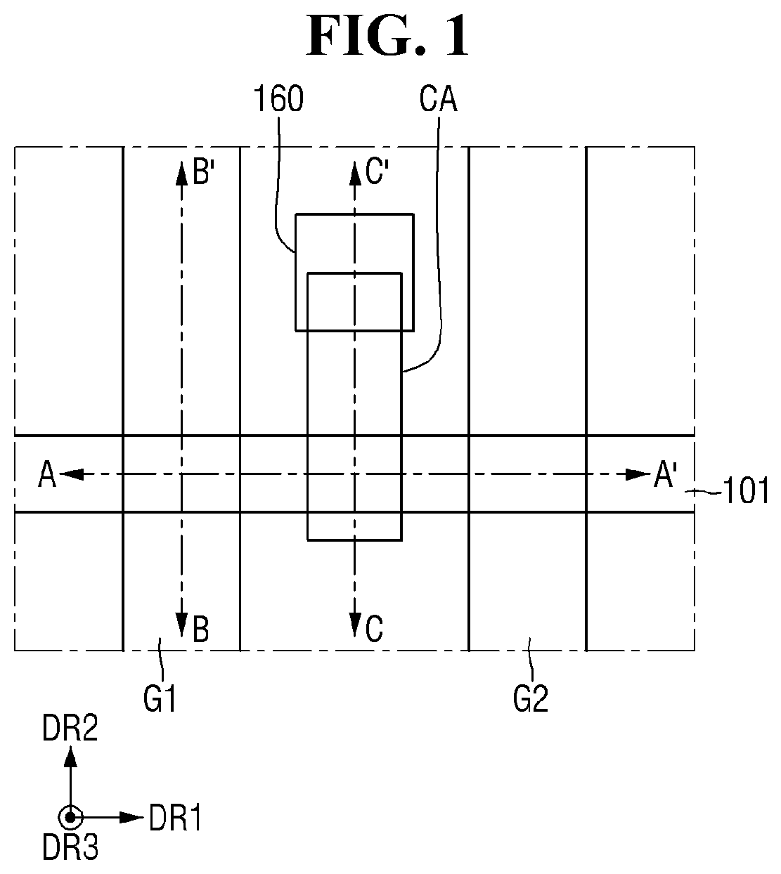
The above and other aspects and features will be more apparent from the following description of embodiments with reference to the attached drawings, in which: is a schematic layout view illustrating a semiconductor device according to some embodiments; is a cross-sectional view taken along line A-A′ of ; is a cross-sectional view taken along line B-B′ of ; is a cross-sectional view taken along line C-C′ of ; is an enlarged view illustrating a region S 1 of ; to 34 are views illustrating intermediate operations of a method of manufacturing a semiconductor device according to some embodiments; is a cross-sectional view illustrating a semiconductor device according to some other embodiments; is an enlarged view illustrating a region S 2 of ; to 41 are views illustrating operations of a method of manufacturing a semiconductor device according to some embodiments; is a cross-sectional view illustrating a semiconductor device according to some other embodiments; is an enlarged view illustrating a region S 3 of ; to 49 are views illustrating operations of a method of manufacturing a semiconductor device according to some embodiments; is a schematic layout view illustrating a semiconductor device according to some other embodiments; is a cross-sectional view taken along line D-D′ of ; and is a cross-sectional view illustrating a semiconductor device according to some other embodiments.
DETAILED DESCRIPTION
Embodiments will now be described with reference to the accompanying drawings. Embodiments described herein are example embodiments, and thus, the present disclosure is not limited thereto, and may be realized in various other forms. Each embodiment provided in the following description is not excluded from being associated with one or more features of another example or another embodiment also provided herein or not provided herein but consistent with the present disclosure. It will be understood that when an element or layer is referred to as being “on,” “connected to” or “coupled to” another element or layer, it can be directly on, connected or coupled to the other element or layer, or intervening elements or layers may be present. By contrast, when an element is referred to as being “directly on,” “directly connected to” or “directly coupled to” another element or layer, there are no intervening elements or layers present. As used herein, the term “and/or” includes any and all combinations of one or more of the associated listed items. Expressions such as “at least one of,” when preceding a list of elements, modify the entire list of elements and do not modify the individual elements of the list. For example, the expression, “at least one of a, b, and c,” should be understood as including only a, only b, only c, both a and b, both a and c, both b and c, or all of a, b, and c. It will be also understood that, even if a certain step or operation of manufacturing an apparatus or structure is described later than another step or operation, the step or operation may be performed later than the other step or operation unless the other step or operation is described as being performed after the step or operation. A semiconductor device according to some embodiments includes a multi-bridge channel field effect transistor (MBCFET™) including a nanosheet by way of example, but embodiments are not limited thereto. In some other embodiments, the semiconductor device may include a fin-type transistor (FinFET) that includes a channel region of a fin-type pattern shape. Hereinafter, a semiconductor device according to some embodiments will be described with reference to to 5 . is a schematic layout view illustrating a semiconductor device according to some embodiments. is a cross-sectional view taken along line A-A′ of . is a cross-sectional view taken along line B-B′ of . is a cross-sectional view taken along line C-C′ of . is an enlarged view illustrating a region S 1 of . Referring to to 5 , the semiconductor device according to some embodiments includes a first substrate 100 , an active pattern 101 , a field insulating layer 105 , first and plurality of second nanosheets NW 1 and NW 2 , a sacrificial layer 110 , a second substrate 120 , a lower wiring layer 130 , a lower wiring insulating layer 135 , first and second gate electrodes G 1 and G 2 , a gate spacer 141 , a gate insulating layer 142 , a capping pattern 143 , a source/drain region SD, a first interlayer insulating layer 150 , a silicide layer 155 , a through via 160 , a through via insulating layer 165 , a source/drain contact CA, first and second gate contacts CB 1 and CB 2 , an etch stop layer 170 , a second interlayer insulating layer 175 , first and second vias V 1 and V 2 , a third interlayer insulating layer 180 , and first to third upper wiring layers 191 , 192 and 193 . The first substrate 100 may be a silicon substrate or a silicon-on-insulator (SOI). Alternatively, the first substrate 100 may include silicon germanium, silicon germanium on insulator (SGOI), indium antimonide, lead telluride compound, indium arsenide, indium phosphide, gallium arsenide, or gallium antimonide, but embodiments are not limited thereto. The first substrate 100 may include a first surface 100 a and a second surface 100 b opposite the first surface 100 a . For example, the first surface 100 a of the first substrate 100 may be an upper surface of the first substrate 100 , and the second surface 100 b of the first substrate 100 may be a lower surface of the first substrate 100 . Hereinafter, each of a first horizontal direction DR 1 and a second horizontal direction DR 2 may be a direction parallel with the first surface 100 a of the first substrate 100 . The second horizontal direction DR 2 may be different from the first horizontal direction DR 1 . The vertical direction DR 3 may be perpendicular to each of the first horizontal direction DR 1 and the second horizontal direction DR 2 . The active pattern 101 may extend in the first horizontal direction DR 1 on the first surface 100 a of the first substrate 100 . The active pattern 101 may protrude from the first surface 100 a of the first substrate 100 in the vertical direction DR 3 . For example, the active pattern 101 may be a portion of the first substrate 100 , or may include an epitaxial layer grown from the first substrate 100 . The field insulating layer 105 may be disposed on the first surface 100 a of the first substrate 100 . The field insulating layer 105 may surround a sidewall of the active pattern 101 . For example, an upper surface of the active pattern 101 may be protrude in the vertical direction DR 3 past an upper surface of the field insulating layer 105 , but embodiments are not limited thereto. In some other embodiments, the upper surface of the active pattern 101 may be formed on the same plane as the upper surface of the field insulating layer 105 . The field insulating layer 105 may include, for example, an oxide layer, a nitride layer, an oxynitride layer, or their combination layer. The plurality of first nanosheets NW 1 may be disposed on the active pattern 101 . The plurality of first nanosheets NW 1 may be disposed at a portion where the active pattern 101 and the first gate electrode G 1 cross each other. The plurality of first nanosheets NW 1 may include a plurality of nanosheets stacked to be spaced apart from each other in the vertical direction DR 3 . The plurality of second nanosheets NW 2 may be disposed on the active pattern 101 . The plurality of second nanosheets NW 2 may be disposed at a portion where the active pattern 101 and the second gate electrode G 2 cross each other. The plurality of second nanosheets NW 2 may be spaced apart from the plurality of first nanosheets NW 1 in the first horizontal direction DR 1 . The plurality of second nanosheets NW 2 may include a plurality of nanosheets stacked to be spaced apart from each other in the vertical direction DR 3 . In , each of the plurality of first and second nanosheets NW 1 and NW 2 is shown to include three nanosheets stacked to be spaced apart from one another in the vertical direction DR 3 , but this is for convenience of description, and embodiments are not limited thereto. In some other embodiment, each of the plurality of first and second nanosheets NW 1 and NW 2 may include four or more nanosheets stacked to be spaced apart from each other in the vertical direction DR 3 . The sacrificial layer 110 may be disposed on the second surface 100 b of the first substrate 100 . An upper surface 110 a of the sacrificial layer 110 may be in contact with the second surface 100 b of the first substrate 100 . For example, the sacrificial layer 110 may be disposed to be conformal. The sacrificial layer 110 may include a material different from that of the first substrate 100 . The sacrificial layer 110 may include a material having an etching selectivity with respect to the material included in the first substrate 100 . For example, the sacrificial layer 110 may include silicon germanium (SiGe). That is, for example, the first substrate 100 may include silicon (Si), and the sacrificial layer 110 may include silicon germanium (SiGe). The second substrate 120 may be disposed on a lower surface 110 b of the sacrificial layer 110 , which is disposed on the second surface 100 b of the first substrate 100 . The second substrate 120 may be in contact with the lower surface 110 b of the sacrificial layer 110 . The second substrate 120 may include a material different from that of the sacrificial layer 110 . The second substrate 120 may include a material having an etching selectivity with respect to the sacrificial layer 110 . For example, the second substrate 120 may include silicon (Si). That is, the second substrate 120 may include silicon (Si), and the sacrificial layer 110 may include silicon germanium (SiGe). The first gate electrode G 1 may extend in the second horizontal direction DR 2 on the active pattern 101 and the field insulating layer 105 . The first gate electrode G 1 may surround the plurality of first nanosheets NW 1 . The second gate electrode G 2 may extend in the second horizontal direction DR 2 on the active pattern 101 and the field insulating layer 105 . The second gate electrode G 2 may be spaced apart from the first gate electrode G 1 in the first horizontal direction DR 1 . The second gate electrode G 2 may surround the plurality of second nanosheets NW 2 . Each of the first and second gate electrodes G 1 and G 2 may include at least one of, for example, titanium nitride (TiN), tantalum carbide (TaC), tantalum nitride (TaN), titanium silicon nitride (TiSiN), tantalum silicon nitride (TaSiN), tantalum titanium nitride (TaTiN), titanium aluminum nitride (TiAlN), tantalum aluminum nitride (TaAlN), tungsten nitride (WN), ruthenium (Ru), titanium aluminum (TiAl), titanium aluminum carbonitride (TiAlC—N), titanium aluminum carbide (TiAlC), titanium carbide (TiC), tantalum carbonitride (TaCN), tungsten (W), aluminum (Al), copper (Cu), cobalt (Co), titanium (Ti), tantalum (Ta), nickel (Ni), platinum (Pt), nickel platinum (Ni—Pt), niobium (Nb), niobium nitride (NbN), niobium carbide (NbC), molybdenum (Mo), molybdenum nitride (MoN), molybdenum carbide (MoC), tungsten carbide (WC), rhodium (Rh), palladium (Pd), iridium (Ir), osmium (Os), silver (Ag), gold (Au), zinc (Zn), vanadium (V), or their combination. Each of the first and second gate electrodes G 1 and G 2 may include a conductive metal oxide, a conductive metal oxynitride, and the like, and may include oxidized forms of the aforementioned materials. The gate spacer 141 may extend in the second horizontal direction DR 2 along both sidewalls of the first gate electrode G 1 on the field insulating layer 105 and the upper surface of the uppermost nanosheet of the plurality of first nanosheets NW 1 . In addition, the gate spacer 141 may extend in the second horizontal direction DR 2 along both sidewalls of the second gate electrode G 2 on the field insulating layer 105 and the upper surface of the uppermost nanosheet of the plurality of second nanosheets NW 2 . The gate spacer 141 may include at least one of, for example, silicon nitride (SiN), silicon oxynitride (SiON), silicon oxide (SiO 2 ), silicon oxycarbonitride (SiOCN), silicon boron nitride (SiBN), silicon oxyboron nitride (SiOBN), silicon oxycarbide (SiOC), or their combination, but embodiments are not limited thereto. The source/drain region SD may be disposed on at least one side of each of the first and second gate electrodes G 1 and G 2 on the active pattern 101 . For example, the source/drain region SD may be disposed between the first gate electrode G 1 and the second gate electrode G 2 on the active pattern 101 . The source/drain region SD may be in contact with each of the plurality of first nanosheets NW 1 and the plurality of second nanosheets NW 2 . For example, an upper surface of the source/drain region SD may be formed to be higher than the upper surface of the uppermost nanosheet of the plurality of first nanosheets NW 1 , but embodiments are not limited thereto. The gate insulating layer 142 may be disposed between each of the first and second gate electrodes G 1 and G 2 and the gate spacer 141 . The gate insulating layer 142 may be disposed between each of the first and second gate electrodes G 1 and G 2 and the active pattern 101 . The gate insulating layer 142 may be disposed between each of the first and second gate electrodes G 1 and G 2 and the field insulating layer 105 . The gate insulating layer 142 may be disposed between the first gate electrode G 1 and the plurality of first nanosheets NW 1 . The gate insulating layer 142 may be disposed between the second gate electrode G 2 and the plurality of second nanosheets NW 2 . The gate insulating layer 142 may be disposed between each of the first and second gate electrodes G 1 and G 2 and the source/drain region SD. For example, the gate insulating layer 142 may be in contact with the source/drain region SD, but embodiments are not limited thereto. In some other embodiments, an inner spacer may be disposed between each of the first and second gate electrodes G 1 and G 2 and the source/drain region SD. The gate insulating layer 142 may include at least one of silicon oxide, silicon oxynitride, silicon nitride, or a high dielectric constant material having a dielectric constant greater than that of the silicon oxide. The high dielectric constant material may include one or more of hafnium oxide, hafnium silicon oxide, hafnium aluminum oxide, lanthanum oxide, lanthanum aluminum oxide, zirconium oxide, zirconium silicon oxide, tantalum oxide, titanium oxide, barium strontium titanium oxide, barium titanium oxide, strontium titanium oxide, yttrium oxide, aluminum oxide, lead scandium tantalum oxide, or lead zinc niobate. The semiconductor device according to some other embodiments may include a negative capacitance (NC) FET based on a negative capacitor. For example, the gate insulating layer 142 may include a ferroelectric material layer having ferroelectric characteristics and a paraelectric material layer having paraelectric characteristics. The ferroelectric material layer may have a negative capacitance, and the paraelectric material layer may have a positive capacitance. For example, when two or more capacitors are connected in series, and the capacitance of each capacitor has a positive value, the total capacitance is more reduced than the capacitance of each individual capacitor. On the other hand, when at least one of capacitances of two or more capacitors connected in series has a negative value, the total capacitance may have a positive value and may be greater than an absolute value of each individual capacitance. When a ferroelectric material layer having a negative capacitance and a paraelectric material layer having a positive capacitance are connected in series, the total capacitance value of the ferroelectric material layer and the paraelectric material layer, which are connected in series, may be increased. Based on the total capacitance value that is increased, a transistor having a ferroelectric material layer may have a subthreshold swing (SS) less than 60 mV/decade at a room temperature. The ferroelectric material layer may have ferroelectric characteristics. The ferroelectric material layer may include at least one of, for example, hafnium oxide, hafnium zirconium oxide, barium strontium titanium oxide, barium titanium oxide, or lead zirconium titanium oxide. In this case, for example, the hafnium zirconium oxide may be a material doped with zirconium (Zr) in hafnium oxide. For another example, the hafnium zirconium oxide may be a compound of hafnium (Hf) and zirconium (Zr) and oxygen (O). The ferroelectric material layer may further include a doped dopant. For example, the dopant may include at least one of aluminum (Al), titanium (Ti), niobium (Nb), lanthanum (La), yttrium (Y), magnesium (Mg), silicon (Si), calcium (Ca), cerium (Ce), dysprosium (Dy), erbium (Er), gadolinium (Gd), germanium (Ge), scandium (Sc), strontium (Sr), or tin (Sn). A type of the dopant included in the ferroelectric material layer may be varied depending on the ferroelectric material of the ferroelectric material layer. When the ferroelectric material layer includes hafnium oxide, the dopant included in the ferroelectric material layer may include at least one of gadolinium (Gd), silicon (Si), zirconium (Zr), aluminum (Al), or yttrium (Y). When the dopant is aluminum (Al), the ferroelectric material layer may include aluminum of 3 at % to 8 at % (atomic %). In this case, a ratio of the dopant may be a ratio of aluminum to a sum of hafnium and aluminum. When the dopant is silicon (Si), the ferroelectric material layer may include silicon of 2 at % to 10 at %. When the dopant is yttrium (Y), the ferroelectric material layer may include yttrium of 2 at % to 10 at %. When the dopant is gadolinium (Gd), the ferroelectric material layer may include gadolinium of 1 at % to 7 at %. When the dopant is zirconium (Zr), the ferroelectric material layer may include zirconium of 50 at % to 80 at %. The paraelectric material layer may have paraelectric characteristics. The paraelectric material layer may include, for example, at least one of silicon oxide or metal oxide having a high dielectric constant. The metal oxide included in the paraelectric material layer may include, but is not limited to, at least one of hafnium oxide, zirconium oxide, or aluminum oxide. The ferroelectric material layer and the paraelectric material layer may include the same material. Although the ferroelectric material layer has ferroelectric characteristics, the paraelectric material layer may not have ferroelectric characteristics. For example, when the ferroelectric material layer and the paraelectric material layer include hafnium oxide, a crystal structure of hafnium oxide included in the ferroelectric material layer is different from that of hafnium oxide included in the paraelectric material layer. The ferroelectric material layer may have a thickness having ferroelectric characteristics. The thickness of the ferroelectric material layer may be, for example, 0.5 nm to 10 nm, but is not limited thereto. Because a threshold thickness indicating ferroelectric characteristics may be varied depending on each ferroelectric material, the thickness of the ferroelectric material layer may be varied depending on the ferroelectric material. For example, the gate insulating layer 142 may include one ferroelectric material layer. For another example, the gate insulating layer 142 may include a plurality of ferroelectric material layers spaced apart from each other. The gate insulating layer 142 may have a stacked layer structure in which a plurality of ferroelectric material layers and a plurality of paraelectric material layers are alternately stacked. The capping pattern 143 may extend in the second horizontal direction DR 2 on each of the first gate electrode G 1 , the gate insulating layer 142 and the gate spacer 141 . Also, the capping pattern 143 may extend in the second horizontal direction DR 2 on each of the second gate electrode G 2 , the gate insulating layer 142 , and the gate spacer 141 . For example, the capping pattern 143 may be in contact with an upper surface of the gate spacer 141 , but embodiments are not limited thereto. In some other embodiments, the capping pattern 143 may be disposed between the gate spacers 141 . The capping pattern 143 may include at least one of, for example, silicon nitride (SiN), silicon oxynitride (SiON), silicon oxide (SiO 2 ), silicon carbonitride (SiCN), silicon oxycarbonitride (SiOCN), or their combination, but embodiments are not limited thereto. The first interlayer insulating layer 150 may be disposed on the field insulating layer 105 . The first interlayer insulating layer 150 may cover the source/drain regions SD. The first interlayer insulating layer 150 may surround a sidewall of each of the gate spacer 141 and the capping pattern 143 . For example, an upper surface of the first interlayer insulating layer 150 may be formed on the same plane as that of the capping pattern 143 , but embodiments are not limited thereto. In some other embodiments, the first interlayer insulating layer 150 may the upper surface of the capping pattern 143 . The first interlayer insulating layer 150 may include, for example, at least one of silicon oxide, silicon nitride, silicon oxynitride, or a low dielectric constant material. For example, the low dielectric constant material may include Fluorinated TetraEthylOrthoSilicate (FTEOS), Hydrogen SilsesQuioxane (HSQ), Bis-benzoCycloButene (BCB), TetraMethylOrthoSilicate (TMOS), OctaMethyleyCycloTetraSiloxane (OMCTS), HexaMethylDiSiloxane (HMDS), TriMethylSilyl Borate (TMSB), DiAcetoxyDitertiaryButoxySiloxane (DADBS), TriMethylSilil Phosphate (TMSP), PolyTetraFluoroEthylene (PTFE), Tonen SilaZen (TOSZ), Fluoride Silicate Glass (FSG), polyimide nanofoams such as polypropylene oxide, Carbon Doped silicon Oxide (CDO), Organo Silicate Glass (OSG), SiLK, Amorphous Fluorinated Carbon, silica aerogels, silica xerogels, mesoporous silica or their combination, but embodiments are not limited thereto. A through via trench 160 T may extend into the second substrate 120 by passing through the first interlayer insulating layer 150 , the field insulating layer 105 , the first substrate 100 , and the sacrificial layer 110 in the vertical direction DR 3 . For example, the through via trench 160 T may be formed between the first gate electrode G 1 and the second gate electrode G 2 . The through via trench 160 T may be spaced apart from each of the first gate electrode G 1 and the second gate electrode G 2 in the first horizontal direction DR 1 . For example, the through via trench 160 T may be spaced apart from the active pattern 101 in the second horizontal direction DR 2 . A first recess R 1 may be formed inside the sacrificial layer 110 . The first recess R 1 may protrude from a first sidewall of the through via trench 160 T in a reverse direction of the second horizontal direction DR 2 . For example, an upper surface of the first recess R 1 may be formed on the same plane as the upper surface of the sacrificial layer 110 . Also, a lower surface of the first recess R 1 may be formed on the same plane as the lower surface of the sacrificial layer 110 . A second recess R 2 may be formed inside the sacrificial layer 110 . The second recess R 2 may protrude in the second horizontal direction DR 2 from a second sidewall of the through via trench 160 T opposite the first sidewall of the through via trench 160 T in the second horizontal direction DR 2 . For example, an upper surface of the second recess R 2 may be formed on the same plane as the upper surface of the sacrificial layer 110 . In addition, a lower surface of the second recess R 2 may be formed on the same plane as the lower surface of the sacrificial layer 110 . Although the first recess R 1 and the second recess R 2 are described to be provided separately, for example, the first recess R 1 and the second recess R 2 may protrude in a lateral direction from the sidewall of the through via trench 160 T and thus may be integrally formed. The through via insulating layer 165 may be disposed along the sidewall of the through via trench 160 T. For example, the through via insulating layer 165 may be disposed to be conformal. The through via insulating layer 165 may include a first portion 165 _ 1 and a second portion 165 _ 2 . The first portion 165 _ 1 of the through via insulating layer 165 may be disposed along the sidewall of the through via trench 160 T. For example, the first portion 165 _ 1 of the through via insulating layer 165 may extend to the upper surface of the first interlayer insulating layer 150 . Also, the first portion 165 _ 1 of the through via insulating layer 165 may extend to the inside of the second substrate 120 . The second portion 165 _ 2 of the through via insulating layer 165 may be disposed inside each of the first recess R 1 and the second recess R 2 . For example, the second portion 165 _ 2 of the through via insulating layer 165 may fill the inside of each of the first recess R 1 and the second recess R 2 . The second portion 165 _ 2 of the through via insulating layer 165 may protrude in a lateral direction from the first portion 165 _ 1 of the through via insulating layer 165 . For example, the second portion 165 _ 2 of the through via insulating layer 165 disposed inside the first recess R 1 may protrude in a reverse direction of the second horizontal direction DR 2 from the first portion 165 _ 1 of the through via insulating layer 165 disposed along the first sidewall of the through via trench 160 T. In addition, the second portion 165 _ 2 of the through via insulating layer 165 disposed inside the second recess R 2 may protrude from the first portion 165 _ 1 of the through via insulating layer 165 disposed along the second sidewall of the through via trench 160 T in the second horizontal direction DR 2 . An upper surface of the second portion 165 _ 2 of the through via insulating layer 165 may be formed on the same plane as the upper surface of the sacrificial layer 110 . In addition, a lower surface of the second portion 165 _ 2 of the through via insulating layer 165 may be formed on the same plane as the lower surface of the sacrificial layer 110 . Although the second portions 165 _ 2 of the through via insulating layer 165 disposed inside the first recess R 1 and the second recess R 2 are described to be provided separately, for example, the second portions 165 _ 2 of the through via insulating layer 165 disposed inside the first recess R 1 and the second recess R 2 may protrude in a lateral direction from the first portion 165 _ 1 of the through via insulating layer 165 and may be integrally formed. The through via insulating layer 165 may include an insulating material. For example, the through via insulating layer 165 may include at least one of silicon nitride (SiN), silicon oxide (SiO 2 ), silicon oxynitride (SiON), silicon oxycarbide (SiOC), or silicon oxycarbonitride (SiOCN), but embodiments are not limited thereto. The through via 160 may be disposed on the through via insulating layer 165 inside the through via trench 160 T. For example, the through via 160 may overlap the sacrificial layer 110 in the second horizontal direction DR 2 . That is, a lower surface of the through via 160 may be formed to be lower than the lower surface 110 b of the sacrificial layer 110 . The through via 160 may include a through via bather layer 161 and a through via filling layer 162 . The through via barrier layer 161 may be disposed on the through via insulating layer 165 along the sidewall of the through via trench 160 T. The through via barrier layer 161 may be disposed along a bottom surface of the through via trench 160 T. For example, the through via barrier layer 161 may be disposed to be conformal. For example, an uppermost surface of the through via barrier layer 161 may be formed on the same plane as that of the first interlayer insulating layer 150 , but embodiments are not limited thereto. The through via barrier layer 161 may include one of, for example, titanium (Ti), titanium nitride (TiN), tantalum (Ta), tantalum nitride (TaN), tantalum carbonitride (TaCN), tungsten (W), tungsten nitride (WN), tungsten carbonitride (WCN), zirconium (Zr), zirconium nitride (ZrN), vanadium (V), vanadium nitride (VN), niobium (Nb), niobium nitride (NbN), and their combination, but embodiments are not limited thereto. The through via filling layer 162 may be disposed on the through via barrier layer 161 inside the through via trench 160 T. The through via filling layer 162 may fill the inside of the through via trench 160 T on the through via barrier layer 161 . For example, an upper surface of the through via filling layer 162 may be formed on the same plane as the uppermost surface of the first interlayer insulating layer 150 , but embodiments are not limited thereto. The through via filling layer 162 may include at least one of, for example, molybdenum (Mo), copper (Cu), carbon (C), silver (Ag), cobalt (Co), tantalum (Ta), indium (In), tin (Sn), zinc (Zn), manganese (Mn), titanium (Ti), magnesium (Mg), chromium (Cr), germanium (Ge), strontium (Sr), platinum (Pt), aluminum (Al), zirconium (Zr), tungsten (W), ruthenium (Ru), iridium (Ir), or rhodium (Rh), but embodiments are not limited thereto. The lower wiring trench 130 T may be formed on the second surface 100 b of the first substrate 100 . For example, the lower wiring trench 130 T may be formed inside the second substrate 120 on the lower surface 110 b of the sacrificial layer 110 . For example, as the lower wiring trench 130 T approaches the lower surface 110 b of the sacrificial layer 110 , its width in the second horizontal direction DR 2 may be reduced. For example, the lower wiring trench 130 T may overlap each of the through via 160 and the through via insulating layer 165 in the vertical direction DR 3 . For example, the lower surface of the second portion 165 _ 2 of the through via insulating layer 165 may be exposed through the lower wiring trench 130 T. Also, the first portion 165 _ 1 of the through via insulating layer 165 and the through via 160 may be exposed through the lower wiring trench 130 T. In this case, the through via barrier layer 161 forming the bottom surface of the through via trench 160 T may be exposed through the lower wiring trench 130 T. For example, a width W 2 of the through via trench 160 T in the second horizontal direction DR 2 , at a position adjacent to the second portion 165 _ 2 of the through via insulating layer 165 , may be smaller than a width W 1 of the second portion 165 _ 2 of the through via insulating layer 165 in the second direction DR 2 . In this case, the width W 1 of the second portion 165 _ 2 of the through via insulating layer 165 in the second horizontal direction DR 2 may be referred to as a width in the second horizontal direction DR 2 between a sidewall of the second portion 165 _ 2 of the through via insulating layer 165 , which is in contact with the sacrificial layer 110 inside the first recess R 1 , and a sidewall of the second portion 165 _ 2 of the through via insulating layer 165 , which is in contact with the sacrificial layer 110 inside the second recess R 2 . For example, the lower surface of the second portion 165 _ 2 of the through via insulating layer 165 disposed inside the first recess R 1 may be in contact with the second substrate 120 disposed on a first sidewall 130 Ts 1 of the lower wiring trench 130 T. In addition, the lower surface of the second portion 165 _ 2 of the through via insulating layer 165 disposed inside the second recess R 2 may be in contact with the second substrate 120 disposed on a second sidewall 130 Ts 2 of the lower wiring trench 130 T opposite the first sidewall 130 Ts 1 of the lower wiring trench 130 T in the second horizontal direction DR 2 . The lower wiring insulating layer 135 may be disposed along the sidewall of the lower wiring trench 130 T. For example, the lower wiring insulating layer 135 may be in contact with the lower surface 110 b of the sacrificial layer 110 . The lower wiring insulating layer 135 may include an insulating material. For example, the lower wiring insulating layer 135 may include the same material as that of the through via insulating layer 165 , but embodiments are not limited thereto. In some other embodiments, the lower wiring insulating layer 135 and the through via insulating layer 165 may include different materials. The lower wiring insulating layer 135 may include at least one of, for example, silicon nitride (SiN), silicon oxide (SiO 2 ), silicon oxynitride (SiON), silicon oxycarbide (SiOC), or silicon oxycarbonitride (SiOCN), but embodiments are not limited thereto. The lower wiring layer 130 may be disposed inside the lower wiring trench 130 T. At least a portion of the lower wiring layer 130 may be disposed inside the second portion 165 _ 2 of the through via insulating layer 165 . An uppermost surface 130 a of the lower wiring layer 130 may be in contact with the second portion 165 _ 2 of the through via insulating layer 165 . Also, the lower wiring layer 130 may be in contact with a lowermost surface of the first portion 165 _ 1 of the through via insulating layer 165 and a lowermost surface of the through via 160 . For example, the lower wiring layer 130 may be in contact with the through via barrier layer 161 forming a bottom surface of the through via 160 . For example, the lower wiring layer 130 may be spaced apart from the through via filling layer 162 in the vertical direction DR 3 , but embodiments are not limited thereto. For example, the lower wiring layer 130 may be either a power rail to which a power source is supplied or a ground rail that is grounded. The uppermost surface 130 a of the lower wiring layer 130 may be formed to be lower than the upper surface of the second portion 165 _ 2 of the through via insulating layer 165 . That is, the uppermost surface 130 a of the lower wiring layer 130 may be formed to be lower than the upper surface 110 a of the sacrificial layer 110 . In addition, the uppermost surface 130 a of the lower wiring layer 130 may be formed to be higher than the lower surface of the second portion 165 _ 2 of the through via insulating layer 165 . That is, the uppermost surface 130 a of the lower wiring layer 130 may be formed to be lower than the lower surface 110 b of the sacrificial layer 110 . For example, a width of the lower wiring layer 130 in the second horizontal direction DR 2 , at a position adjacent to the second portion 165 _ 2 of the through via insulating layer 165 , may be smaller than the width W 1 of the second portion 165 _ 2 of the through via insulating layer 165 in the second horizontal direction DR 2 . For example, at least a portion of the lower wiring insulating layer 135 may be disposed between the lower wiring layer 130 and the first portion 165 _ 1 of the through via insulating layer 165 , but embodiments are not limited thereto. The lower wiring layer 130 may include a lower wiring barrier layer 131 and a lower wiring filling layer 132 . The lower wiring barrier layer 131 may be disposed along sidewalls and upper surface of the lower wiring trench 130 T. For example, the lower wiring barrier layer 131 may be disposed to be conformal. For example, at least a portion of the lower wiring barrier layer 131 may be disposed inside the second portion 165 _ 2 of the through via insulating layer 165 . The lower wiring layer 130 may be insulated from the second substrate 120 through the lower wiring insulating layer 135 . The lower wiring barrier layer 131 includes one of, for example, cobalt (Co), titanium (Ti), titanium nitride (TiN), tantalum (Ta), tantalum nitride (TaN), tantalum carbonitride (TaCN), tungsten (W), tungsten nitride (WN), tungsten carbonitride (WCN), zirconium (Zr), zirconium nitride (ZrN), vanadium (V), vanadium nitride (VN), niobium (Nb), niobium nitride (NbN), and their combination, but embodiments are not limited thereto. The lower wiring filling layer 132 may be disposed on the lower wiring barrier layer 131 inside the lower wiring trench 130 T. The lower wiring filling layer 132 may fill the inside of the lower wiring trench 130 T on the lower wiring barrier layer 131 . For example, a lower surface of the lower wiring filling layer 132 may be formed on the same plane as the lower surface of the second substrate 120 , but embodiments are not limited thereto. The lower wiring filling layer 132 includes at least one of, for example, molybdenum (Mo), copper (Cu), carbon (C), silver (Ag), cobalt (Co), tantalum (Ta), indium (In), tin (Sn), zinc (Zn), manganese (Mn), titanium (Ti), magnesium (Mg), chromium (Cr), germanium (Ge), strontium (Sr), platinum (Pt), aluminum (Al), zirconium (Zr), tungsten (W), ruthenium (Ru), iridium (Ir), or rhodium (Rh), but embodiments are not limited thereto. The source/drain contact CA may be disposed inside the first interlayer insulating layer 150 . The source/drain contact CA may be connected to the source/drain region SD. For example, an upper surface of the source/drain contact CA may be formed on the same plane as that of the through via 160 . For example, the upper surface of the source/drain contact CA may be formed on the same plane as the upper surface of the first interlayer insulating layer 150 , but embodiments are not limited thereto. The source/drain contact CA may be in contact with the through via 160 . For example, the source/drain contact CA may be in contact with the through via filling layer 162 . The source/drain contact CA may overlap the through via 160 in the vertical direction DR 3 . Although the source/drain contact CA is shown as being formed as a single layer in , this is for convenience of description, and embodiments are not limited thereto. That is, the source/drain contact CA may be formed of a multi-layer. The source/drain contact CA may include a conductive material. The silicide layer 155 may be disposed between the source/drain region SD and the source/drain contact CA. The silicide layer 155 may be disposed along a boundary surface between the source/drain region SD and the source/drain contact CA. The silicide layer 155 may include, for example, a metal silicide material. The first gate contact CB 1 may be connected to the first gate electrode G 1 by passing through the capping pattern 143 in the vertical direction DR 3 . The second gate contact CB 2 may be connected to the second gate electrode G 2 by passing through the capping pattern 143 in the vertical direction DR 3 . For example, upper surfaces of the first gate contact CB 1 and the second gate contact CB 2 may be formed on the same plane as the upper surface of the capping pattern 143 , but embodiments are not limited thereto. Although show that each of the first and second gate contacts CB 1 and CB 2 is formed as a single layer, this is for convenience of description, and embodiments are not limited thereto. That is, each of the first and second gate contacts CB 1 and CB 2 may be formed of a multi-layer. Each of the first and second gate contacts CB 1 and CB 2 may include a conductive material. The etch stop layer 170 may be disposed on upper surfaces of the first interlayer insulating layer 150 , the capping pattern 143 , the first and second gate contacts CB 1 and CB 2 , the source/drain contact CA, and the through via 160 . to 4 show that the etch stop layer 170 is formed as a single layer, but embodiments are not limited thereto. In some other embodiments, the etch stop layer 170 may be formed of a multi-layer. The etch stop layer 170 may include at least one of, for example, aluminum oxide, aluminum nitride, hafnium oxide, zirconium oxide, silicon oxide, silicon nitride, silicon oxynitride, or a low dielectric constant material. The second interlayer insulating layer 175 may be disposed on the etch stop layer 170 . For example, the second interlayer insulating layer 175 may include at least one of silicon oxide, silicon nitride, silicon oxynitride, or a low dielectric constant material. The first via V 1 may be connected to each of the first gate contact CB 1 and the second gate contact CB 2 by passing through the second interlayer insulating layer 175 and the etch stop layer 170 in the vertical direction DR 3 . The second via V 2 may be connected to the source/drain contact CA by passing through the second interlayer insulating layer 175 and the etch stop layer 170 in the vertical direction DR 3 . Although to 4 show that each of the first and second vias V 1 and V 2 is formed as a single layer, this is for convenience of description, and embodiments are not limited thereto. That is, each of the first and second vias V 1 and V 2 may be formed of a multi-layer. Each of the first and second vias V 1 and V 2 may include a conductive material. The third interlayer insulating layer 180 may be disposed on the second interlayer insulating layer 175 . The third interlayer insulating layer 180 may include at least one of, for example, silicon oxide, silicon nitride, silicon oxynitride, or a low dielectric constant material. Each of the first to third upper wiring layers 191 , 192 and 193 may be disposed inside the third interlayer insulating layer 180 . For example, each of the first to third upper wiring layers 191 , 192 and 193 may be sequentially spaced apart from one another in the first horizontal direction DR 1 . For example, each of the first to third upper wiring layers 191 , 192 and 193 may extend in the second horizontal direction DR 2 , but embodiments are not limited thereto. For example, the first upper wiring layer 191 may be disposed on the first via V 1 disposed on the first gate contact CB 1 . The first upper wiring layer 191 may be connected to the first via V 1 disposed on the first gate contact CB 1 . The second upper wiring layer 192 may be disposed on the second via V 2 disposed on the source/drain contact CA. The second upper wiring layer 192 may be connected to the second via V 2 disposed on the source/drain contact CA. The third upper wiring layer 193 may be disposed on the first via V 1 disposed on the second gate contact CB 2 . The third upper wiring layer 193 may be connected to the first via V 1 disposed on the second gate contact CB 2 . Although to 4 show that each of the first to third upper wiring layers 191 , 192 and 193 is formed as a single layer, this is for convenience of description, and embodiments are not limited thereto. That is, each of the first to third upper wiring layers 191 , 192 and 193 may be formed of a multi-layer. Each of the first to third upper wiring layers 191 , 192 and 193 may include a conductive material. In the semiconductor device according to some embodiments, the lower wiring layer 130 which is a power rail or a ground rail may be disposed below the first substrate 100 , the sacrificial layer 110 may be disposed between the lower surface of the first substrate 100 and the lower wiring layer 130 , and the through via insulating layer 165 , which overlaps the lower wiring layer 130 in the vertical direction DR 3 , may be disposed inside the sacrificial layer 110 . The through via insulating layer 165 disposed inside the sacrificial layer 110 may serve as an etch stop layer in the process of forming the lower wiring trench 130 T in which the lower wiring layer 130 is formed. Therefore, the semiconductor device according to some embodiments may improve reliability of a connection relation between the through via 160 and the lower wiring layer 130 by preventing the lower wiring trench 130 T from being excessively or less etched. Hereinafter, a method of manufacturing a semiconductor device according to some embodiments will be described with reference to to 34 . to 34 are views illustrating operations of a method of manufacturing a semiconductor device shown in to 5 . Referring to , a sacrificial layer 110 and a first substrate 100 may be sequentially formed on a second substrate 120 . For example, the sacrificial layer 110 may be epitaxially grown to be formed on the second substrate 120 . A stacked structure 10 may be formed on the first substrate 100 . The stacked structure 10 may include first semiconductor layers 11 and second semiconductor layers 12 , which are alternately stacked on the first substrate 100 . For example, a first semiconductor layer 11 may be formed at a lowermost portion of the stacked structure 10 , and a second semiconductor layer 12 may be formed at an uppermost portion of the stacked structure 10 , but embodiments are not limited thereto. In some other embodiments, a first semiconductor layer 11 may be also formed at the uppermost portion of the stacked structure 10 . The first semiconductor layer 11 may include, for example, silicon germanium (SiGe). The second semiconductor layer 12 may include, for example, silicon (Si). Referring to , a portion of the stacked structure 10 may be etched. While the stacked structure 10 is being etched, a portion of the first substrate 100 may be also etched. Through the etching process, an active pattern 101 may be defined below the stacked structure 10 on a first surface 100 a that is an upper surface of the first substrate 100 . The active pattern 101 may extend in the first horizontal direction DR 1 . A field insulating layer 105 may be formed on the first surface 100 a of the first substrate 100 . The field insulating layer 105 may surround sidewalls of the active pattern 101 . For example, an upper surface of the active pattern 101 may be formed to be higher than an upper surface of the field insulating layer 105 . A pad oxide layer 20 may be formed to cover the upper surface of the field insulating layer 105 , exposed sidewalls of the active pattern 101 and sidewalls and upper surface of the stacked structure 10 . For example, the pad oxide layer 20 may be formed to be conformal. The pad oxide layer 20 may include, for example, silicon oxide (SiO 2 ). Referring to to 12 , first and second dummy gates DG 1 and DG 2 , and first and second dummy capping patterns DC 1 and DC 2 which extend in the second horizontal direction DR 2 on the pad oxide layer 20 may be formed on the stacked structure 10 and the field insulating layer 105 . The first dummy capping pattern DC 1 may be formed on the first dummy gate DG 1 . Also, the second dummy capping pattern DC 2 may be formed on the second dummy gate DG 2 . The second dummy gate DG 2 and the second dummy capping pattern DC 2 may be respectively spaced apart from the first dummy gate DG 1 and the first dummy capping pattern DC 1 in the first horizontal direction DR 1 . While the first and second dummy gates DG 1 and DG 2 and the first and second dummy capping patterns DC 1 and DC 2 are being formed, the remaining pad oxide layer 20 , except a portion overlapped with each of the first and second dummy gates DG 1 and DG 2 in the vertical direction DR 3 on the first substrate 100 , may be removed. A spacer material layer SM may be formed to cover sidewalls of each of the first and second dummy gates DG 1 and DG 2 , sidewalls and upper surface of each of the first and second dummy capping patterns DC 1 and DC 2 , exposed sidewalls and upper surface of the stacked structure 10 , and the upper surface of the field insulating layer 105 . For example, the spacer material layer SM may be formed to be conformal. The spacer material layer SM may include at least one of, for example, silicon nitride (SiN), silicon oxycarbonitride (SiOCN), silicon boron carbonitride (SiBCN), silicon carbonitride (SiCN), silicon oxynitride (SiON), or their combination. Referring to , the stacked structure ( 10 of to 12 ) may be etched using the first and second dummy capping patterns DC 1 and DC 2 and the first and second dummy gates DG 1 and DG 2 as masks to form a source/drain trench ST. For example, the source/drain trench ST may extend into the active pattern 101 . While the source/drain trench ST is being formed, the spacer material layer (SM of to 12 ) formed on the upper surfaces of the first and second dummy capping patterns DC 1 and DC 2 and a portion of each of the first and second dummy capping patterns DC 1 and DC 2 may be removed. The spacer material layer (SM of to 12 ) remaining on sidewalls of each of the first and second dummy capping patterns DC 1 and DC 2 and the first and second dummy gates DG 1 and DG 2 may be referred to as a gate spacer 141 . After the source/drain trench ST is formed, the second semiconductor layers ( 12 of to 12 ) remaining below the first dummy gate DG 1 may be referred to as a plurality of first nanosheets NW 1 . In addition, after the source/drain trench ST is formed, the second semiconductor layers ( 12 of to 12 ) remaining below the second dummy gate DG 2 may be referred to as a plurality of second nanosheets NW 2 . Referring to , a source/drain region SD may be formed inside the source/drain trench ST. For example, an upper surface of the source/drain region SD may be formed to be higher than an upper surface of the uppermost nanosheet of the plurality of first nanosheets NW 1 , but embodiments are not limited thereto. Referring to to 19 , a first interlayer insulating layer 150 may be formed to cover sidewalls and upper surface of the source/drain region SD, the gate spacer 141 , and each of the first and second dummy capping patterns (DC 1 and DC 2 of ). The upper surfaces of the first and second dummy gates (DG 1 and DG 2 of ) may be exposed through a planarization process. Each of the first and second dummy gates (DG 1 and DG 2 of ), the pad oxide layer ( 20 of ) and the first semiconductor layer ( 11 of ) may be removed. A portion from which the first dummy gate (DG 1 of ) is removed may be referred to as a first gate trench GT 1 . In addition, a portion from which the second dummy gate (DG 2 of ) is removed may be referred to as a second gate trench GT 2 . Referring to , a gate insulating layer 142 may be formed at the portion from which each of the first and second dummy gates (DG 1 and DG 2 of ), the pad oxide layer ( 20 of ) and the first semiconductor layer ( 11 of ) is removed. For example, the gate insulating layer 142 may be formed to be conformal. A first gate electrode G 1 may be formed on the gate insulating layer 142 at the portion from which each of the first dummy gate (DG 1 of ), the pad oxide layer ( 20 of ) and the sacrificial layer ( 11 of ) is removed. The first gate electrode G 1 may surround the plurality of first nanosheets NW 1 . In addition, a second gate electrode G 2 may be formed on the gate insulating layer 142 at the portion from which each of the second dummy gate (DG 2 of ), the pad oxide layer ( 20 of ) and the first semiconductor layer ( 11 of ) is removed. The second gate electrode G 2 may surround the plurality of second nanosheets NW 2 . A portion of an upper portion of each of the gate spacer 141 , the gate insulating layer 142 , the first gate electrode G 1 and the second gate electrode G 2 may be etched. A capping pattern 143 may be formed at the portion from which a portion of the upper portion of each of the gate spacer 141 , the gate insulating layer 142 , the first gate electrode G 1 and the second gate electrode G 2 is etched. For example, an upper surface of the capping pattern 143 may be formed on the same plane as an upper surface of the first interlayer insulating layer 150 , but embodiments are not limited thereto. Referring to , a through via trench 160 T, which extends into the second substrate 120 by passing through the first interlayer insulating layer 150 , the field insulating layer 105 , the first substrate 100 and the sacrificial layer 110 in the vertical direction DR 3 , may be formed. For example, the through via trench 160 T may be spaced apart from the source/drain region SD in the second horizontal direction DR 2 . Also, the through via trench 160 T may be formed between the first gate electrode G 1 and the second gate electrode G 2 . Referring to , a portion of the sacrificial layer 110 , which is exposed to the through via trench 160 T, may be etched. A portion of the sacrificial layer 110 may be etched through a wet etching process. Through this etching process, a first recess R 1 and a second recess R 2 may be formed inside the sacrificial layer 110 adjacent to the through via trench 160 T. Referring to , a through via insulating layer 165 may be formed along sidewalls and a bottom surface of the through via trench 160 T. In addition, the through via insulating layer 165 may fill the inside of each of the first recess R 1 and the second recess R 2 . For example, the through via insulating layer 165 may be formed to be conformal. In this case, a portion of the through via insulating layer 165 formed along the sidewalls and the bottom surface of the through via trench 160 T may be referred to as a first portion 165 _ 1 of the through via insulating layer 165 . Also, a portion of the through via insulating layer 165 formed inside each of the first recess R 1 and the second recess R 2 may be referred to as a second portion 165 _ 2 of the through via insulating layer 165 . A through via 160 , which includes a through via barrier layer 161 and a through via filling layer 162 , may be formed on the through via insulating layer 165 inside the through via trench 160 T. For example, the through via barrier layer 161 may be formed on the through via insulating layer 165 inside the through via trench 160 T. For example, the through via barrier layer 161 may be formed to be conformal. The through via filling layer 162 may be formed on the through via barrier layer 161 inside the through via trench 160 T. The through via filling layer 162 may fill the inside of the through via trench 160 T. Referring to to 27 , a first gate contact CB 1 and a second gate contact CB 2 , which are respectively connected to the first gate electrode G 1 and the second gate electrode G 2 , may be formed by passing through the capping pattern 143 in the vertical direction DR 3 . In addition, a source/drain contact CA connected to the source/drain region SD may be formed by passing through the first interlayer insulating layer 150 in the vertical direction DR 3 . A silicide layer 155 may be formed between the source/drain region SD and the source/drain contact CA. For example, the source/drain contact CA may be also formed at a portion from which a portion of each sidewall of the through via 160 and the through via insulating layer 165 is etched. For this reason, the source/drain contact CA may be in contact with the through via 160 . Also, the source/drain contact CA may overlap the through via 160 in the vertical direction DR 3 . Referring to to 30 , an etch stop layer 170 and a second interlayer insulating layer 175 may be sequentially formed on an upper surface of each of the first interlayer insulating layer 150 , the capping pattern 143 , the first and second gate contacts CB 1 and CB 2 , the source/drain contact CA and the through via 160 . A first via V 1 connected to each of the first gate contact CB 1 and the second gate contact CB 2 may be formed by passing through the second interlayer insulating layer 175 and the etch stop layer 170 in the vertical direction DR 3 . In addition, a second via V 2 connected to the source/drain contact CA may be formed by passing through the second interlayer insulating layer 175 and the etch stop layer 170 in the vertical direction DR 3 . A third interlayer insulating layer 180 may be formed on an upper surface of each of the second interlayer insulating layer 175 , the first via V 1 and the second via V 2 . First to third upper wiring layers 191 , 192 and 193 may be formed inside the third interlayer insulating layer 180 . For example, the first to third upper wiring layers 191 , 192 and 193 may be sequentially spaced apart from one another in the first horizontal direction DR 1 . For example, the first to third upper wiring layers 191 , 192 and 193 may extend in the second horizontal direction DR 2 . The first upper wiring layer 191 may be connected to the first via V 1 on the first gate contact CB 1 . The second upper wiring layer 192 may be connected to the second via V 2 on the source/drain contact CA. The third upper wiring layer 193 may be connected to the first via V 1 on the second gate contact CB 2 . Referring to , after the manufacturing process shown in to 30 is performed, upper and lower portions may be inverted. In a state that the upper and lower portions are inverted, a lower wiring trench 130 T may be formed inside the second substrate 120 . The lower wiring trench 130 T may be formed inside the second substrate 120 overlapped with the second portion 165 _ 2 of the through via insulating layer 165 in the vertical direction DR 3 . The through via insulating layer 165 may be exposed through the lower wiring trench 130 T. Referring to , a lower wiring insulating layer 135 may be formed inside the lower wiring trench 130 T and on the exposed surface of the second substrate 120 . For example, the lower wiring insulating layer 135 may be formed to be conformal. Referring to , for example, a portion of the lower wiring insulating layer 135 may be removed by an etch-back etching process. For example, the lower wiring insulating layer 135 formed on the uppermost surface of the first portion 165 _ 1 of the through via insulating layer 165 and the upper surface of the second portion 165 _ 2 of the through via insulating layer 165 may be removed through the etch-back etching process. For example, a portion of the second portion 165 _ 2 of the through via insulating layer 165 may be also removed. However, for example, a portion of the lower wiring insulating layer 135 formed on the first portion 165 _ 1 of the through via insulating layer 165 may remain without being etched, but embodiments are not limited thereto. In addition, the lower wiring insulating layer 135 formed on the surface of the second substrate 120 adjacent to the lower wiring trench 130 T may be removed through the etch-back etching process. Referring to , a lower wiring barrier layer 131 and a lower wiring filling layer 132 may be sequentially formed inside the lower wiring trench 130 T. Therefore, the lower wiring layer 130 may be formed inside the lower wiring trench 130 T. After the manufacturing process is performed, the semiconductor device shown in to 5 may be manufactured by inversion of the upper and lower portions. Hereinafter, a semiconductor device according to some other embodiments will be described with reference to . The following description will be based on differences from the semiconductor device shown in to 5 . is a cross-sectional view illustrating a semiconductor device according to some other embodiments. is an enlarged view illustrating a region S 2 of . Referring to , in the semiconductor device according to some other embodiments, a lower wiring layer 230 may be disposed inside a lower interlayer insulating layer 285 . The lower interlayer insulating layer 285 may include at least one of, for example, silicon oxide, silicon nitride, silicon oxynitride, or a low dielectric constant material. For example, the lower interlayer insulating layer 285 may be disposed on the lower surface 110 b of the sacrificial layer 110 . The lower interlayer insulating layer 285 may be in contact with the lower surface 110 b of the sacrificial layer 110 . A lower surface of the second portion 165 _ 2 of the through via insulating layer 165 may be in contact with the lower interlayer insulating layer 285 disposed on a first sidewall 230 Ts 1 of a lower wiring trench 230 T. In addition, the lower surface of the second portion 165 _ 2 of the through via insulating layer 165 may be in contact with the lower interlayer insulating layer 285 disposed on a second sidewall 230 Ts 2 of the lower wiring trench 230 T. For example, a width W 22 of the through via trench 160 T in the second horizontal direction DR 2 , which is adjacent to the second portion 165 _ 2 of the through via insulating layer 165 , may be smaller than the width W 1 of the second portion 165 _ 2 of the through via insulating layer 165 in the second horizontal direction DR 2 . For example, at least a portion of the lower wiring layer 230 may be disposed inside the second portion 165 _ 2 of the through via insulating layer 165 . An uppermost surface 230 a of the lower wiring layer 230 may be in contact with the second portion 165 _ 2 of the through via insulating layer 165 . Also, the lower wiring layer 230 may be in contact with each of the lowermost surface of the first portion 165 _ 1 of the through via insulating layer 165 and the lowermost surface of the through via 160 . For example, the lower wiring layer 230 may be in contact with the through via barrier layer 161 forming the bottom surface of the through via 160 . For example, the uppermost surface 230 a of the lower wiring layer 230 may be formed to be lower than the upper surface of the second portion 165 _ 2 of the through via insulating layer 165 . That is, the uppermost surface 230 a of the lower wiring layer 230 may be formed to be lower than the upper surface 110 a of the sacrificial layer 110 . In addition, the uppermost surface 230 a of the lower wiring layer 230 may be formed to be higher than the lower surface of the second portion 165 _ 2 of the through via insulating layer 165 . That is, the uppermost surface 230 a of the lower wiring layer 230 may be formed to be lower than the lower surface 110 b of the sacrificial layer 110 . For example, the lower wiring layer 230 may include a lower wiring barrier layer 231 and a lower wiring filling layer 232 . The lower wiring barrier layer 231 may be disposed along sidewalls and upper surface of the lower wiring trench 230 T. For example, the lower wiring bather layer 231 may be disposed to be conformal. The lower wiring bather layer 231 may be in contact with the lower interlayer insulating layer 285 . The lower wiring filling layer 232 may be disposed on the lower wiring barrier layer 231 inside the lower wiring trench 230 T. The lower wiring filling layer 232 may fill the inside of the lower wiring trench 230 T on the lower wiring barrier layer 231 . Hereinafter, a method of manufacturing the semiconductor device shown in will be described with reference to to 41 . The following description will be based on differences from the method of manufacturing a semiconductor device, which is shown in to 34 . Referring to , after the manufacturing process shown in to 30 is performed, upper and lower portions may be inverted. In a state that the upper and lower portions are inverted, the second substrate ( 120 of ) may be removed. Therefore, each of the sacrificial layer 110 and the through via insulating layer 165 may be exposed. Referring to , a lower interlayer insulating layer 285 may be formed to cover the exposed sacrificial layer 110 and the exposed through via insulating layer 165 . Referring to , a lower wiring trench 230 T may be formed inside the lower interlayer insulating layer 285 . The lower wiring trench 230 T may be formed inside the lower interlayer insulating layer 285 overlapped with the second portion 165 _ 2 of the through via insulating layer 165 in the vertical direction DR 3 . The through via insulating layer 165 may be exposed through the lower wiring trench 230 T. Referring to , for example, a portion of the through via insulating layer 165 may be removed by an etch-back etching process. For example, the through via insulating layer 165 formed on the through via 160 may be removed through the etch-back etching process, so that the through via barrier layer 161 may be exposed. For example, the second portion 165 _ 2 of the through via insulating layer 165 may be also removed. Referring to , a lower wiring barrier layer 231 and a lower wiring filling layer 232 may be sequentially formed inside the lower wiring trench 230 T. Therefore, the lower wiring layer 230 may be formed inside the lower wiring trench 230 T. After the manufacturing process is performed, the semiconductor device shown in may be manufactured by inversion of the upper and lower portions. Hereinafter, a semiconductor device according to some other embodiments will be described with reference to . The following description will be based on differences from the semiconductor device shown in to 5 . is a cross-sectional view illustrating a semiconductor device according to some other embodiments. is an enlarged view illustrating a region S 3 of . Referring to , in the semiconductor device according to some other embodiments, a lower wiring layer 330 may be disposed inside a lower interlayer insulating layer 385 . The lower interlayer insulating layer 385 may include at least one of, for example, silicon oxide, silicon nitride, silicon oxynitride, or a low dielectric constant material. For example, the lower interlayer insulating layer 385 may be disposed on the lower surface 110 b of the sacrificial layer 110 . The lower interlayer insulating layer 385 may be in contact with the lower surface 110 b of the sacrificial layer 110 . A lower surface of the second portion 165 _ 2 of the through via insulating layer 165 may be in contact with the lower interlayer insulating layer 385 disposed on a first sidewall 330 Ts 1 of a lower wiring trench 330 T. In addition, the lower surface of the second portion 165 _ 2 of the through via insulating layer 165 may be in contact with the lower interlayer insulating layer 385 disposed on a second sidewall 330 Ts 2 of the lower wiring trench 330 T. For example, a width W 32 of the through via trench 160 T in the second horizontal direction DR 2 , which is adjacent to the second portion 165 _ 2 of the through via insulating layer 165 , may be smaller than the width W 1 of the second portion 165 _ 2 of the through via insulating layer 165 in the second horizontal direction DR 2 . For example, an uppermost surface 330 a of the lower wiring layer 330 may be in contact with the second portion 165 _ 2 of the through via insulating layer 165 . The uppermost surface 330 a of the lower wiring layer 330 may be formed on the same plane as the upper surface of the lower interlayer insulating layer 385 . Also, the lower wiring layer 330 may be in contact with each of the lowermost surface of the first portion 165 _ 1 of the through via insulating layer 165 and the lowermost surface of the through via 160 . For example, the lower wiring layer 330 may be in contact with each of the through via barrier layer 161 and the through via filling layer 162 . For example, the lower wiring layer 330 may include a lower wiring barrier layer 331 and a lower wiring filling layer 332 . The lower wiring barrier layer 331 may be disposed along sidewalls and upper surface of the lower wiring trench 330 T. For example, the lower wiring barrier layer 331 may be disposed to be conformal. The lower wiring barrier layer 331 may be in contact with the lower interlayer insulating layer 385 . The lower wiring filling layer 332 may be disposed on the lower wiring barrier layer 331 inside the lower wiring trench 330 T. The lower wiring filling layer 332 may fill the inside of the lower wiring trench 330 T on the lower wiring barrier layer 331 . Hereinafter, a method of manufacturing the semiconductor device shown in will be described with reference to to 49 . The following description will be based on differences from the method of manufacturing a semiconductor device, which is shown in to 34 . to 49 are views illustrating intermediate operations of a method of manufacturing a semiconductor device shown in . Referring to , after the manufacturing process shown in to 30 is performed, upper and lower portions may be inverted. In a state that the upper and lower portions are inverted, the second substrate ( 120 of ) may be removed. Therefore, each of the sacrificial layer 110 and the through via insulating layer 165 may be exposed. Referring to , a lower interlayer insulating layer 385 may be formed to cover the exposed sacrificial layer 110 and the exposed through via insulating layer 165 . Referring to , a portion of the lower interlayer insulating layer 385 and a portion of the through via insulating layer 165 may be etched by a planarization process. For example, the through via barrier layer 161 formed on the through via filling layer 162 may be also etched. Therefore, the uppermost surface of the through via insulating layer 165 , the uppermost surface of the through via barrier layer 161 and the uppermost surface of the through via filling layer 162 may be exposed, respectively. For example, a portion of the lower interlayer insulating layer 385 may remain on the second portion 165 _ 2 of the through via insulating layer 165 and the sacrificial layer 110 . Referring to , a lower interlayer insulating layer 385 may be additionally formed on the uppermost surface of the through via insulating layer 165 , the uppermost surface of the through via barrier layer 161 , the uppermost surface of the through via filling layer 162 , and the remaining lower interlayer insulating layer 385 . Referring to , a lower wiring trench 330 T may be formed inside the lower interlayer insulating layer 385 . The lower wiring trench 330 T may be formed inside the lower interlayer insulating layer 385 overlapped with the second portion 165 _ 2 of the through via insulating layer 165 in the vertical direction DR 3 . The through via insulating layer 165 , the uppermost surface of the through via barrier layer 161 and the uppermost surface of the through via filling layer 162 may be respectively exposed through the lower wiring trench 330 T. Referring to , a lower wiring barrier layer 331 and a lower wiring filling layer 332 may be sequentially formed inside the lower wiring trench 330 T. Therefore, the lower wiring layer 330 may be formed inside the lower wiring trench 330 T. After the manufacturing process is performed, the semiconductor device shown in may be manufactured by inversion of the upper and lower portions. Hereinafter, a semiconductor device according to some other embodiments will be described with reference to . The following description will be based on differences from the semiconductor device shown in to 5 . is a schematic layout view illustrating a semiconductor device according to some other embodiments. is a cross-sectional view taken along line D-D′ of . Referring to , in the semiconductor device according to some other embodiments, a through via 460 may be spaced apart from a source/drain contact CA 4 in the second horizontal direction DR 2 . For example, a through via trench 460 T may extend into the second substrate 120 by passing through the first interlayer insulating layer 150 , the field insulating layer 105 , the first substrate 100 , and the sacrificial layer 110 in the vertical direction DR 3 . A through via insulating layer 465 may be disposed along sidewalls of the through via trench 460 T. That is, a first portion 465 _ 1 of the through via insulating layer 465 may be disposed along the sidewalls of the through via trench 460 T. For example, the through via 460 may be disposed on the through via insulating layer 465 inside the through via trench 460 T. The through via 460 may include a through via bather layer 461 disposed on the through via insulating layer 465 and a through via filling layer 462 disposed on the through via bather layer 461 . For example, an upper surface of each of the through via insulating layer 465 and the through via 460 may be formed on the same plane as the upper surface of the first interlayer insulating layer 150 . The third via V 3 may pass through the second interlayer insulating layer 175 and the etch stop layer 170 in the vertical direction DR 3 . The third via V 3 may connect the through via 460 with the second upper wiring layer 192 . Hereinafter, a semiconductor device according to some other embodiments will be described with reference to . The following description will be based on differences from the semiconductor device shown in to 5 . is a cross-sectional view illustrating a semiconductor device according to some other embodiments. Referring to , in the semiconductor device according to some other embodiments, a through via 560 may be spaced apart from the source/drain contact CA 4 in the second horizontal direction DR 2 . For example, a through via trench 560 T may extend into the second substrate 120 by passing through the second interlayer insulating layer 175 , the etch stop layer 170 , the first interlayer insulating layer 150 , the field insulating layer 105 , the first substrate 100 and the sacrificial layer 110 in the vertical direction DR 3 . A through via insulating layer 565 may be disposed along sidewalls of the through via trench 560 T. That is, a first portion 565 _ 1 of the through via insulating layer 565 may be disposed along the sidewalls of the through via trench 560 T. For example, the through via 560 may be disposed on the through via insulating layer 565 inside the through via trench 560 T. The through via 560 may include a through via bather layer 561 disposed on the through via insulating layer 565 and a through via filling layer 562 disposed on the through via barrier layer 561 . For example, an upper surface of each of the through via insulating layer 565 and the through via 560 may be formed on the same plane as the upper surface of the second interlayer insulating layer 175 . Each of the through via insulating layer 565 and the through via 560 may be in contact with the second upper wiring layer 192 . That is, the through via 560 may be directly connected to the second upper wiring layer 192 . While aspects of embodiments have been particularly shown and described, it will be understood that various changes in form and details may be made therein without departing from the spirit and scope of the following claims.
Figures (20)
Citations
This patent cites (67)
- US8877626
- US9112045
- US9214351
- US9553105
- US9634097
- US9941293
- US9991277
- US9997462
- US10170638
- US10453824
- US10818792
- US10872859
- US10892337
- US10985057
- US11121080
- US11264327
- US11380706
- US11974434
- US12191352
- US12230692
- US12356680
- US12369353
- US2011/0068466
- US2014/0269078
- US2014/0273373
- US2016/0043100
- US2016/0104719
- US2016/0133643
- US2017/0186765
- US2019/0067321
- US2019/0067323
- US2019/0081068
- US2019/0287864
- US2020/0044023
- US2020/0266169
- US2020/0402906
- US2021/0043649
- US2021/0134721
- US2021/0210613
- US2021/0217846
- US2021/0335709
- US2021/0351079
- US2022/0037496
- US2022/0052157
- US2022/0059460
- US2022/0077062
- US2022/0122970
- US2022/0131004
- US2022/0181500
- US2023/0011153
- US2023/0031546
- US2023/0122379
- US2023/0178618
- US2024/0128335
- US2024/0213316
- US2024/0243171
- US2024/0290855
- US2024/0321989
- US2025/0072116
- US2025/0098264
- US2025/0107209
- US2025/0220961
- US2025/0234712
- US2025/0241012
- US2025/0255106
- US2025/0261428
- US2008/035261