Abstract
An oscillator device includes a current generating circuit, a current source and an oscillator circuit. The current generating circuit generates first, second, third and fourth currents. The current source generates a first reference current according to the first current and the second current and a second reference current according to the third current and the fourth current. The oscillator circuit receives the first reference current and the second reference current and generates an oscillating signal. The temperature coefficient of the oscillator circuit is compensated for by the first reference current and the second reference current. At least two of the first current, the second current, the third current and the fourth current are different. The first reference current is different from the second reference current.
Claims (19)
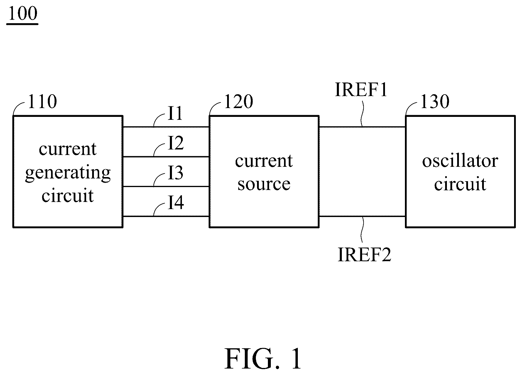
1 . An oscillator device, comprising: a current generating circuit, configured to generate a first current, a second current, a third current and a fourth current; a current source, coupled to the current generating circuit, and configured to generate a first reference current according to the first current and the second current, and generate a second reference current according to the third current and the fourth current; and an oscillator circuit, coupled to the current source, and configured to receive the first reference current and the second reference current and generate an oscillating signal, wherein a temperature coefficient of the oscillator circuit is compensated for by the first reference current and the second reference current; wherein at least two of the first current, the second current, the third current and the fourth current are different, and the first reference current is different from the second reference current; wherein the first reference current and the second reference current change according to a change of temperature.
Show 18 dependent claims
2 . The oscillator device as claimed in claim 1 , wherein the first current and the third current are positive temperature coefficient currents, and the second current and the fourth current are negative temperature coefficient currents.
3 . The oscillator device as claimed in claim 1 , wherein the current generating circuit is a bandgap on a system on a chip.
4 . The oscillator device as claimed in claim 1 , wherein the current source adjusts a ratio of the first current and the second current and a ratio of the third current and the fourth current according to the change of temperature.
5 . The oscillator device as claimed in claim 1 , wherein the current source comprises: a first current source unit, having a first terminal, a second terminal, a third terminal and a fourth terminal, wherein the first terminal of the first current source unit receives a reference voltage, the second terminal of the first current source unit receives the first current, the third terminal of the first current source unit receives the second current, and the fourth terminal of the first current source unit generates the first reference current; and a second current source unit, having a first terminal, a second terminal, a third terminal and a fourth terminal, wherein the first terminal of the second current source unit receives the reference voltage, the second terminal of the second current source unit receives the third current, the third terminal of the second current source unit receives the fourth current, and the fourth terminal of the second current source unit generates the second reference current.
6 . The oscillator device as claimed in claim 5 , wherein the reference voltage is a system voltage.
7 . The oscillator device as claimed in claim 1 , wherein the oscillator circuit is a frequency locked loop oscillator.
8 . The oscillator device as claimed in claim 7 , wherein the oscillator circuit comprises: a resistor, having a first terminal and a second terminal, wherein first terminal of the resistor receives the first reference current, and the second terminal of the resistor receives a reference voltage; an operation amplifier, having a first input terminal, a second input terminal and an output terminal, wherein the first input terminal of the operation amplifier is coupled to the first terminal of the resistor; a first capacitor, having a first terminal and a second terminal, wherein the first terminal of the first capacitor is coupled to the second input terminal of the operation amplifier, and the second terminal of the first capacitor is coupled to the output terminal of the operation amplifier; a filter unit, having an input terminal and an output terminal, wherein the input terminal of the filter unit is coupled to the output terminal of the operation amplifier; an oscillator unit, having an input terminal and an output terminal, wherein the input terminal of the oscillator unit is coupled to the output terminal of the filter unit, and the output terminal of the oscillator unit generates the oscillating signal; a logic unit, having an input terminal and an output terminal, wherein the input terminal of the logic unit is coupled to the output terminal of the oscillator unit, and the output terminal of the logic unit generates a first control signal, a second control signal and a third control signal; a first switch unit, having a first terminal, a second terminal and a control terminal, wherein the first terminal of the first switch unit receives the second reference current, and the control terminal of the first switch unit is coupled to the output terminal of the logic unit and receives the first control signal; a second capacitor, having a first terminal and a second terminal, wherein the first terminal of the second capacitor is coupled to the second terminal of the first switch unit, and the second terminal of the second capacitor receives the reference voltage; and a second switch unit, having a first terminal, a second terminal and a control terminal, wherein the first terminal of the second switch unit is coupled to the first terminal of the second capacitor, the second terminal of the second switch unit is coupled to the second terminal of the second capacitor, and the control terminal of the second switch unit is coupled to the output terminal of the logic unit and receives the second control signal; a third switch unit, having a first terminal, a second terminal and a control terminal, wherein the first terminal of the third switch unit is coupled to the second terminal of the first switch unit, the second terminal of the third switch unit is coupled to the second input terminal of the operation amplifier, and the control terminal of the third switch unit is coupled to the output terminal of the logic unit and receives the third control signal.
9 . The oscillator device as claimed in claim 8 , wherein the oscillator unit is a voltage-controlled oscillator.
10 . The oscillator device as claimed in claim 8 , wherein the resistor is a positive temperature coefficient resistor or a negative temperature coefficient resistor.
11 . The oscillator device as claimed in claim 8 , wherein the reference voltage is a ground voltage.
12 . The oscillator device as claimed in claim 8 , wherein a temperature coefficient of the first reference current and a temperature coefficient of the second reference current are related to a temperature coefficient of the resistor.
13 . The oscillator device as claimed in claim 8 , wherein when a value of the resistor changes according to a change of temperature, the current source adjusts a ratio of the first current and the second current to adjust the first reference current, and the current source adjusts a ratio of the third current and the fourth current to adjust the second reference current.
14 . The oscillator device as claimed in claim 1 , wherein the oscillator circuit is an RC oscillator.
15 . The oscillator device as claimed in claim 14 , wherein the oscillator circuit comprises: a resistor, having a first terminal and a second terminal, wherein the first terminal of the resistor receives the first reference current, and the second terminal of the resistor receives the reference voltage; a comparator, having a first input terminal, a second input terminal and an output terminal, wherein the first input terminal of the comparator is coupled to the first terminal of the resistor, and the output terminal of the comparator generates the oscillating signal; a logic unit, having an input terminal and an output terminal, wherein the input terminal of the logic unit is coupled to the output terminal of the comparator, and the output terminal of the logic unit generates a first control signal and a second control signal; a first switch unit, having a first terminal, a second terminal and a control terminal, wherein the first terminal of the first switch unit is coupled to the second reference current, the second terminal of the first switch unit is coupled to the second input terminal of the comparator and the control terminal of the first switch unit is coupled to the output terminal of the logic unit and receives the first control signal; a capacitor, having a first terminal and a second terminal, wherein the first terminal of the capacitor is coupled to the second terminal of the first switch unit, and the second terminal of the capacitor receives the reference voltage; and a second switch unit, having a first terminal, a second terminal and a control terminal, wherein the first terminal of the second switch unit is coupled to the first terminal of the capacitor, the second terminal of the second switch unit is coupled to the second terminal of the capacitor, and the control terminal of the second switch unit is coupled to the output terminal of the logic unit and receives the second control signal.
16 . The oscillator device as claimed in claim 15 , wherein the resistor is a positive temperature coefficient resistor or a negative temperature coefficient resistor.
17 . The oscillator device as claimed in claim 15 , wherein the reference voltage is a ground voltage.
18 . The oscillator device as claimed in claim 15 , wherein a temperature coefficient of the first reference current and a temperature coefficient of the second reference current are related to a temperature coefficient of the resistor.
19 . The oscillator device as claimed in claim 15 , wherein when a value of the resistor changes according to a change of temperature, the current source adjusts a ratio of the first current and the second current to adjust the first reference current, and the current source adjusts a ratio of the third current and the fourth current to adjust the second reference current.
Full Description
Show full text →
CROSS REFERENCE TO RELATED APPLICATIONS
This application claims the benefit of U.S. Provisional Application No. 63/511,917, filed Jul. 5, 2023, the entirety of which is incorporated by reference herein.
BACKGROUND
OF THE DISCLOSURE Field of the Disclosure The disclosure relates to an oscillator, and, in particular, to an oscillator device that compensates for the temperature coefficient. Description of the Related Art Generally, for lower cost, a crystal oscillator (xtal) is replaced with on-chip oscillator (OSC). In some applications, the frequency variation of the temperature needs to be as small as possible. However, most OSCs use two temperature coefficient (TC) types of resistors to compensate for the frequency variation of the temperature. Due to cost considerations, two TC types of resistors are not available for some processes. Therefore, a new design for a circuit structure is needed to solve the problem described above. BRIEF
SUMMARY
OF THE DISCLOSURE The disclosure provides an oscillator device, thereby effectively compensating for the temperature coefficient of the oscillator device without the need for two temperature coefficient types of resistors, so that the frequency of the oscillator device is stabilized and not affected by the change of temperature. An embodiment of the disclosure provides an oscillator device, which includes a current generating circuit, a current source and an oscillator circuit. The current generating circuit is configured to generate a first current, a second current, a third current and a fourth current. The current source is coupled to the current generating circuit, and is configured to generate a first reference current according to the first current and the second current, and generate a second reference current according to the third current and the fourth current. The oscillator circuit is coupled to the current source, and is configured to receive the first reference current and the second reference current and generate an oscillating signal, wherein the temperature coefficient of the oscillator circuit is compensated for by the first reference current and the second reference current. At least two of the first current, the second current, the third current and the fourth current are different. The first reference current is different from the second reference current. According to the oscillator device disclosed by the disclosure, the current generating circuit generates the first current, the second current, the third current and the fourth current. The current source generates the first reference current according to the first current and the second current, and generates the second reference current according to the third current and the fourth current. The oscillator circuit receives the first reference current and the second reference current and generate the oscillating signal. The temperature coefficient of the oscillator circuit is compensated for by the first reference current and the second reference current. At least two of the first current, the second current, the third current and the fourth current are different. The first reference current is different from the second reference current. Therefore, the temperature coefficient of the oscillator device may be effectively compensated for without the need for two temperature coefficient types of resistors, so that the frequency of the oscillator device is stabilized and not affected by the change of temperature.
BRIEF DESCRIPTION OF THE DRAWINGS
The disclosure can be more fully understood by reading the subsequent detailed description and examples with references made to the accompanying drawings, wherein: is a schematic view of an oscillator device according to an embodiment of the disclosure; is a detailed schematic view of a current source and an oscillator circuit in ; and is another detailed schematic view of a current source and an oscillator circuit in .
DETAILED DESCRIPTION
OF THE DISCLOSURE Technical terms of the disclosure are based on general definition in the technical field of the disclosure. If the disclosure describes or explains one or some terms, definition of the terms is based on the description or explanation of the disclosure. Each of the disclosed embodiments has one or more technical features. In possible implementation, a person skilled in the art would selectively implement all or some technical features of any embodiment of the disclosure or selectively combine all or some technical features of the embodiments of the disclosure. In each of the following embodiments, the same reference number represents the same or a similar element or component. is a schematic view of an oscillator device according to an embodiment of the disclosure. Please refer to . The oscillator device 100 includes a current generating circuit 110 , a current source 120 and an oscillator circuit 130 . The current generating circuit 110 may generate a first current I 1 , a second current I 2 , a third current I 3 and a fourth current I 4 . The current source 120 is coupled to the current generating circuit 110 . The current source 120 may receive the first current I 1 , the second current I 2 , the third current I 3 and the fourth current I 4 . The current source 120 may generate a first reference current IREF 1 according to the first current I 1 and the second current I 2 , and generate a second reference current IREF 2 according to the third current I 3 and the fourth current I 4 . For example, the current source may mix the first current I 1 and the second current I 2 to generate the first reference current IREF 1 , and mix the third current I 3 and the fourth current I 4 to generate a second reference current IREF 2 . The oscillator circuit 130 is coupled to the current source 120 . The oscillator 130 may receive the first reference current IREF 1 and the second reference current IREF 2 and generate an oscillating signal. In the embodiment, the temperature coefficient of the oscillator circuit 130 may be compensated for by the first reference current IREF 1 and the second reference current IREF 2 . In the embodiment, at least two of the first current I 1 , the second current I 2 , the third current I 3 and the fourth current I 4 . For example, magnitudes of at least two of the first current I 1 , the second current I 2 , the third current I 3 and the fourth current I 4 are different, but the disclosure is not limited thereto. In some embodiments, the magnitudes of the first current I 1 and the second current I 2 are different, or the magnitudes of the second current I 2 and the third current I 3 are different, or the magnitudes of the third current I 3 and the fourth current I 4 are different, or the magnitudes of the fourth current I 4 and the first current I 1 are different. In some embodiments, the magnitudes of the first current I 1 , the second current I 2 and the third current I 3 are different, or the magnitudes the second current I 2 , the third current I 3 and the fourth current I 4 are different, or the magnitudes of the third current I 3 , the fourth current I 4 and the first current I 1 are different. In some embodiments, the magnitudes of all of the first current I 1 , the second current I 2 , the third current I 3 and the fourth current I 4 are different. In addition, in the embodiment, the first reference current IREF 1 is different from the second reference current IREF 2 . In some embodiments, the first current I 1 and the third current I 3 are, for example, positive temperature coefficient currents, and the second I 2 and the fourth current I 4 are, for example, negative temperature coefficient currents. That is, the current generating circuit 110 may generate different temperature coefficient currents. Furthermore, the positive temperature coefficient currents may be related to proportional to absolute temperature (PTAT), and the negative temperature coefficient currents may be related to complimentary to absolute temperature (CTAT). In some embodiments, the current generating circuit 110 is, for example, a bandgap on a system on a chip (SOC), but the disclosure is not limited thereto. In other embodiments, the current generating circuit 110 may also be any suitable circuit that may generate different temperature coefficient currents. In some embodiments, the first reference current IREF 1 and the second reference current IREF 2 may change according to a change of temperature. Furthermore, the current source 120 may adjust the ratio of the first current I 1 and the second current I 2 , and the current source 120 may adjust the ratio of the third current I 3 and the fourth current I 4 according to the change of temperature. Therefore, the temperature coefficient of the oscillator device 100 may be effectively compensated for without the need for two temperature coefficient types of resistors, so that the frequency of the oscillating signal generated by the oscillator device 100 (oscillator circuit 130 ) is stabilized and not affected by the change of temperature. In some embodiments, the oscillator circuit 130 may be, for example, a frequency locked loop (FLL) oscillator, but the disclosure is not limited thereto. In some embodiments, the oscillator circuit 130 may be, for example, an RC oscillator, but the disclosure is not limited thereto. is a detailed schematic view of a current source and an oscillator circuit in . Please refer to . The current source 120 may include a first current source unit 210 and a second current source 220 . The first current source unit has a first terminal, a second terminal, a third terminal and a fourth terminal. The first terminal of the first current source unit 210 may receive a reference voltage V 1 . In some embodiments, the reference voltage V 1 may be, for example, a system voltage, but the disclosure is not limited thereto. The second terminal of the first current source unit 210 may receive the first current I 1 . The third terminal of the first current source unit 210 may receive the second current I 2 . The fourth terminal of the first current source unit 210 may generate the first reference current IREF 1 . The second current source unit 220 has a first terminal, a second terminal, a third terminal and a fourth terminal. The first terminal of the second current source unit 220 may receive the reference voltage V 1 . The second terminal of the second current source unit 220 may receive the third current I 3 . The third terminal of the second current source unit 220 may receive the fourth current I 4 . The fourth terminal of the second current source unit 220 may generate the second reference current IREF 2 . The oscillator circuit 130 may include a resistor RREF 1 , an operation amplifier (OPAMP) 230 , a first capacitor CINT, a filter unit 240 , an oscillator unit 250 , a logic unit 260 , a first switch unit SW 1 , a second capacitor CR 1 , a second switch unit SW 2 and a third switch unit SW 3 . The resistor RREF 1 has a first terminal and a second terminal. The first terminal of the resistor RREF 1 may receive the first reference current IREF, and generate a voltage VREF 1 . The second terminal of the resistor RREF 1 may receive a reference voltage V 2 . In some embodiments, the reference voltage V 2 may be, for example, a ground voltage, but the disclosure is not limited thereto. In some embodiments, the resistor RREF 1 may be any type of resistor, such as a positive temperature coefficient resistor or a negative temperature coefficient resistor, but the disclosure is not limited thereto. The operation amplifier 230 has a first input terminal, a second input terminal and an output terminal. The first input terminal of the operation amplifier 230 is coupled to the first terminal of the resistor RREF 1 , and may receive the voltage VREF 1 . In the embodiment, the first input terminal of the operation amplifier 230 is a positive input terminal, and the second input terminal of the operation amplifier 230 is a negative input terminal, but the disclosure is not limited thereto. The first capacitor CINT has a first terminal and a second terminal. The first terminal of the first capacitor CINT is coupled to the second input terminal of the operation amplifier 230 . The second terminal of the first capacitor CINT is coupled to the output terminal of the operation amplifier 230 . The filter unit 240 has an input terminal and an output terminal. The input terminal of the filter unit 240 is coupled to the output terminal of the operation amplifier 230 . The oscillator unit 250 has an input terminal and an output terminal. The input terminal of the oscillator 250 is coupled to the output terminal of the filter unit 240 . The output terminal of the oscillator unit 250 may generate the oscillating signal. In some embodiments, the oscillator unit 250 may be, for example, a voltage-controlled oscillator (VCO), but the disclosure is not limited thereto. The logic unit 260 has an input terminal and an output terminal. The input terminal of the logic unit 260 is coupled to the output terminal of the oscillator unit 250 . The output terminal of the logic unit 260 may generate a first control signal CS 1 , a second control signal CS 2 and a third control signal CS 3 . The first switch unit SW 1 has a first terminal, a second terminal and a control terminal. The first terminal of the first switch unit SW 1 may receive the second reference current IREF 2 . The control terminal of the first switch unit SW 1 is coupled to the output terminal of the logic unit 260 and may receive the first control signal CS 1 . That is, the first switch unit SW 1 is turned on or turned off according to the first control signal CS 1 . The second capacitor CR 1 has a first terminal and a second terminal. The first terminal of the second capacitor CR 1 is coupled to the second terminal of the first switch unit SW 1 . The second terminal of the second capacitor CR 1 may receive the reference voltage V 2 . The second switch unit SW 2 has a first terminal, a second terminal and a control terminal. The first terminal of the second switch unit SW 2 is coupled to the first terminal of the second capacitor CR 1 . The second terminal of the second switch unit SW 2 is coupled to the second terminal of the second capacitor CR 1 . That is, the second switch unit SW 2 is coupled to the second capacitor CR 1 in parallel. The control terminal of the second switch unit SW 2 is coupled to the output terminal of the logic unit 260 and may receive the second control signal CS 2 . That is, the second switch unit SW 2 is turned on or turned off according to the second control signal CS 2 . The third switch unit SW 3 has a first terminal, a second terminal and a control terminal. The first terminal of the third switch unit SW 3 is coupled to the second terminal of the first switch unit SW 1 . The second terminal of the third switch unit SW 3 is coupled to the second input terminal of the operation amplifier 230 . The control terminal of the third switch unit SW 3 is coupled to the output terminal of the logic unit 260 and may receive the third control signal CS 3 . That is, the third switch unit SW 3 is turned on or turned off according to the third control signal CS 3 . In some embodiments, the first switch unit SW 1 , the second switch unit SW 2 and the third switch unit SW 3 are turned on in sequence. In some embodiments, the temperature coefficient of the first reference current IREF 1 and the temperature coefficient of the second reference current IREF 2 are related to the temperature coefficient of the resistor RREF 1 . That is, when the value of the resistor RREF 1 changes according to a change of the temperature, the value of the first reference current IREF 1 and the value of the second reference current IREF 2 may also change accordingly. For example, the frequency of the oscillating signal of the oscillating circuit 130 may be expressed by equation (1). F OSC = IREF 2 × N DIV 2 × CR × IREF 1 × RREF , ( 1 ) wherein F OSC is the frequency of the oscillating signal, IREF 2 is the second reference current, CR is the second capacitor, IREF 1 is the first reference current, RREF 1 is the resistor, N DIV is a coefficient. According to equation (1), it can be seen that when the value of the resistor RREF 1 increases according to the change of temperature, the first current source unit 210 (the current source 120 ) may adjust the ratio of the first current I 1 and the second current I 2 to adjust the first reference current IREF 1 (for example, decreasing the first reference current IREF 1 ), and the second source unit 220 (the current source 120 ) may the ratio of the third current I 3 and the fourth current I 4 to adjust the second reference current IREF 2 (for example, increasing the second reference current IREF 2 ). In addition, when the value of the resistor RREF 1 decreases according to the change of temperature, the first current source unit 210 (the current source 120 ) may adjust the ratio of the first current I 1 and the second current I 2 to adjust the first reference current IREF 1 (for example, increasing the first reference current IREF 1 ), and the second source unit 220 (the current source 120 ) may the ratio of the third current I 3 and the fourth current I 4 to adjust the second reference current IREF 2 (for example, decreasing the second reference current IREF 2 ). That is, when the value of the resistor RREF 1 changes (for example, increasing or decreasing) according to the change of temperature, the current source 120 (such as the first current source unit 210 and the second current source unit 220 ) may adjust the ratio of the first current I 1 and the second current I 2 to adjust the first reference current IREF 1 and the ratio of the third current I 3 and the fourth current I 4 to adjust the second reference current IREF 2 . Therefore, the temperature coefficient the resistor RREF 1 may be effectively compensated for by the first reference current IREF 1 and the second reference current IREF 2 , so that the frequency of the oscillating signal F OSC of the oscillator device 100 may be stabilized and may not affected by the change of temperature. is another detailed schematic view of a current source and an oscillator circuit in . Please refer to . The current source 120 may include a first current source unit 210 and a second current source 220 . In the embodiment, the first current source unit 210 and the second current source 220 in are the same as or similar to the first current source unit 210 and the second current source 220 in . Accordingly, the first current source unit 210 and the second current source 220 in may refer to the description of the embodiment of , and the description thereof is not repeated herein. The oscillator circuit 130 may include a resistor RREF 2 , a comparator 310 , a logic unit 320 , a first switch unit SW 4 , a capacitor CR 2 and a second switch unit SW 5 . The resistor RREF 2 has a first terminal and a second terminal. The first terminal of the resistor RREF 2 may receive the first reference current IREF 2 , and generate a voltage VREF 2 . The second terminal of the resistor RREF 2 may receive the reference voltage V 2 . In some embodiments, the reference voltage V 2 may be, for example, a ground voltage, but the disclosure is not limited thereto. In some embodiments, the resistor RREF 2 may be any type of resistor, such as a positive temperature coefficient resistor or a negative temperature coefficient resistor, but the disclosure is not limited thereto. The comparator 310 has a first input terminal, a second input terminal and an output terminal. The first input terminal of the comparator 310 is coupled to the first terminal of the resistor RREF 2 and may receive the voltage VREF 2 . The output terminal of the comparator 310 may generate the oscillating signal. In the embodiment, the first input terminal of the comparator 310 is a positive input terminal, and the second input terminal of the comparator 310 is a negative input terminal, but the disclosure is not limited thereto. The logic unit 320 has an input terminal and an output terminal. The input terminal of the logic unit 320 is coupled to the output terminal of the comparator 310 . The output terminal of the logic unit 320 may generate a first control signal CS 1 and a second control signal CS 2 . The first switch unit SW 4 has a first terminal, a second terminal and a control terminal. The first terminal of the first switch unit SW 4 is coupled to the second reference current IREF 2 . The second terminal of the first switch unit SW 4 is coupled to the second input terminal of the comparator 310 . The control terminal of the first switch unit SW 4 is coupled to the output terminal of the logic unit 320 and may receive the first control signal CS 4 . That is, the first switch unit SW 4 is turned on or turned off according to the first control CS 4 ; The capacitor CR 2 has a first terminal and a second terminal. The first terminal of the capacitor CR 2 is coupled to the second terminal of the first switch unit SW 4 . The second terminal of the capacitor CR 2 may receive the reference voltage V 2 . The second switch unit SW 5 has a first terminal, a second terminal and a control terminal. The first terminal of the second switch unit SW 5 is coupled to the first terminal of the capacitor CR 2 . The second terminal of the second switch unit SW 5 is coupled to the second terminal of the capacitor CR 2 . That is, the second switch unit SW 5 is coupled to the capacitor CR 2 in parallel. The control terminal of the second switch unit SW 5 is coupled to the output terminal of the logic unit 320 and may receive the second control signal CS 5 . That is, the second switch unit SW 5 is turned on or turned off according to the second control signal CS 2 . In some embodiments, the first switch unit SW 4 and the second switch unit SW 5 are turned on in sequence. In some embodiments, the temperature coefficient of the first reference current IREF 1 and the temperature coefficient of the second reference current IREF 2 are related to the temperature coefficient of the resistor RREF 2 . That is, when the value of the resistor RREF 2 changes according to a change of temperature, the value of the first reference current IREF 1 and the value of the second reference current IREF 2 may also change accordingly. In some embodiments, when the value of the resistor RREF 2 changes according to the change of temperature, the current source 120 may adjust the ratio of the first current I 1 and the second current I 2 to adjust the first reference current IREF 1 and the ratio of the third current I 3 and the fourth current I 4 to adjust the second reference current IREF 2 . Therefore, the temperature coefficient the resistor RREF 2 may be effectively compensated for by the first reference current IREF 1 and the second reference current IREF 2 , so that the frequency of the oscillating signal of the oscillator device 100 may be stabilized and may not affected by the change of temperature. In summary, according to the oscillator device disclosed by the disclosure, the current generating circuit generates the first current, the second current, the third current and the fourth current. The current source generates the first reference current according to the first current and the second current, and generates the second reference current according to the third current and the fourth current. The oscillator circuit receives the first reference current and the second reference current and generate the oscillating signal. The temperature coefficient of the oscillator circuit is compensated for by the first reference current and the second reference current. At least two of the first current, the second current, the third current and the fourth current are different. The first reference current is different from the second reference current. Therefore, the temperature coefficient of the oscillator device may be effectively compensated for without the need for two temperature coefficient types of resistors, so that the frequency of the oscillator device is stabilized and not affected by the change of temperature. While the disclosure has been described by way of example and in terms of the preferred embodiments, it should be understood that the disclosure is not limited to the disclosed embodiments. On the contrary, it is intended to cover various modifications and similar arrangements (as would be apparent to those skilled in the art). Therefore, the scope of the appended claims should be accorded the broadest interpretation so as to encompass all such modifications and similar arrangements.
Figures (3)
Citations
This patent cites (2)
- US2017/0255220
- US2022/0311424