Flyback Power Converter and Control Method Thereof
Abstract
A flyback power converter includes a transformer, a voltage clamping circuit, a main switch element and a control circuit. The voltage clamping circuit includes a first capacitor and a clamping switch element. The first capacitor is electrically connected with a primary winding of the transformer. The clamping switch element is electrically connected between the capacitor and the primary winding. The control circuit detects a capacitor voltage of the first capacitor and a current flowing through the clamping switch element. If the capacitor voltage is greater than a reference voltage, the clamping switch element is turned on. If the capacitor voltage is not greater than the reference voltage and the current flowing through the clamping switch element is lower than a reference current value, the clamping switch element is turned off.
Claims (16)
1 . A control method for a flyback power converter, the control method comprising steps of: (a) providing the flyback power converter, wherein the flyback power converter comprises a transformer, a voltage clamping circuit, a main switch element and a control circuit, the voltage clamping circuit comprises a first capacitor and a clamping switch element, a first terminal of the first capacitor is electrically connected with a first terminal of a primary winding of the transformer, a first terminal of the clamping switch element is electrically connected with a second terminal of the primary winding, a second terminal of the clamping switch element is electrically connected with a second terminal of the first capacitor, and a first terminal of the main switch element and the first terminal of the clamping switch element are electrically connected with the second terminal of the primary winding; (b) the control circuit detecting a capacitor voltage between the second terminal and the first terminal of the first capacitor and detecting a current flowing through the clamping switch element, wherein the first terminal of the first capacitor is a negative terminal, the second terminal of the first capacitor is a positive terminal, and a direction of the current flowing from the first terminal of the clamping switch element to the second terminal of the clamping switch element is defined as a forward direction; (c) the control circuit determining whether the capacitor voltage is greater than a reference voltage, wherein when the capacitor voltage is greater than the reference voltage, the clamping switch element is turned on, and then a step (d) is conducted, wherein when the capacitor voltage is not greater than the reference voltage, the control method returns to conduct the step (b) again; (d) the control circuit determining whether the capacitor voltage is lower than or equal to the reference voltage, wherein when the capacitor voltage is lower than or equal to the reference voltage, a step (e) is conducted, wherein when the capacitor voltage is greater than the reference voltage, the step (d) is conducted again; (e) the control circuit determining whether the current flowing through the clamping switch element is lower than a reference current value, wherein when the current flowing through the clamping switch element is lower than the reference current value, a step (f) is conducted, wherein when the current flowing through the clamping switch element is not lower than the reference current value, the control method returns to conduct the step (d) again; and (f) turning off the clamping switch element under control of the control circuit.
9 . A flyback power converter, comprising: a transformer comprising a primary winding and a secondary winding; a main switch element comprising a first terminal, a second terminal and a control terminal, wherein the first terminal of the main switch element is electrically connected with a second terminal of the primary winding; a voltage clamping circuit comprising a first capacitor and a clamping switch element, wherein a first terminal of the first capacitor is electrically connected with a first terminal of the primary winding, a first terminal of the clamping switch element is electrically connected with the second terminal of the primary winding, and a second terminal of the clamping switch element is electrically connected with a second terminal of the first capacitor; and a control circuit detecting a capacitor voltage of the first capacitor and a current flowing through the clamping switch element, wherein when the capacitor voltage is greater than a reference voltage, the clamping switch element is turned on under control of the control circuit, wherein after the clamping switch element is turned on, when the capacitor voltage is lower than or equal to the reference voltage and the current flowing through the clamping switch element is lower than a reference current value, the clamping switch element is turned off under control of the control circuit.
Show 14 dependent claims
2 . The control method according to claim 1 , wherein the reference voltage is greater than a product of a transformation ratio of the transformer and an output voltage of the flyback power converter, and the reference voltage is less than 1.5 times the product of the transformation ratio of the transformer and the output voltage of the flyback power converter.
3 . The control method according to claim 1 , wherein the reference current value is zero or a negative value.
4 . The control method according to claim 1 , wherein the control circuit is an IC chip.
5 . The control method according to claim 1 , wherein the control circuit comprises a first pin, a second pin, a third pin and a fourth pin, wherein the first pin is electrically connected with the first terminal of the first capacitor, the second pin is electrically connected with the second terminal of the first capacitor and the second terminal of the clamping switch element, the third pin is electrically connected with a control terminal of the clamping switch element, and the fourth pin is electrically connected with the first terminal of the clamping switch element.
6 . The control method according to claim 5 , wherein the flyback power converter further comprises a bootstrap circuit, wherein the bootstrap circuit comprises a diode and a bootstrap capacitor, an anode of the diode is electrically connected with a voltage source, and a cathode of the diode is electrically connected with the bootstrap capacitor in series.
7 . The control method according to claim 1 , wherein a gate-source charge (Qgs) of the clamping switch element is lower than 10 nC.
8 . The control method according to claim 1 , wherein the reverse recovery time of a body diode of the clamping switch element is lower than 100 ns.
10 . The flyback power converter according to claim 9 , wherein the reference voltage is greater than a product of a transformation ratio of the transformer and an output voltage of the flyback power converter, and the reference voltage is less than 1.5 times the product of the transformation ratio of the transformer and the output voltage of the flyback power converter.
11 . The flyback power converter according to claim 9 , wherein the reference current value is zero or a negative value.
12 . The flyback power converter according to claim 9 , wherein the control circuit is an IC chip.
13 . The flyback power converter according to claim 9 , wherein the control circuit comprises a first pin, a second pin, a third pin and a fourth pin, wherein the first pin is electrically connected with the first terminal of the first capacitor, the second pin is electrically connected with the second terminal of the first capacitor and the second terminal of the clamping switch element, the third pin is electrically connected with a control terminal of the clamping switch element, and the fourth pin is electrically connected with the first terminal of the clamping switch element.
14 . The flyback power converter according to claim 13 , wherein the flyback power converter further comprises a bootstrap circuit, wherein the bootstrap circuit comprises a diode and a bootstrap capacitor, an anode of the diode is electrically connected with a voltage source, and a cathode of the diode is electrically connected with the bootstrap capacitor in series.
15 . The flyback power converter according to claim 9 , wherein a gate-source charge (Qgs) of the clamping switch element is lower than 10 nC.
16 . The flyback power converter according to claim 9 , wherein the reverse recovery time of a body diode of the clamping switch element is lower than 100 ns.
Full Description
Show full text →
CROSS-REFERENCE TO RELATED APPLICATION
This application claims priority to China Patent Application No. 202310098910.7, filed on Feb. 8, 2023, the entire contents of which are incorporated herein by reference for all purposes.
FIELD OF THE INVENTION
The present disclosure relates to a power converter, and more particularly to a flyback power converter and a control method of the flyback power converter.
BACKGROUND OF THE INVENTION
Generally, due to the simple control mechanism and low cost, flyback power converters have been widely used in low-power power supply products. Due to the leakage inductance of the internal transformer in the flyback power converter, the switch element in the flyback power converter has a high voltage stress when it is turned off. In order to overcome this problem, the existing flyback power converter usually uses an RCD clamping circuit with a resistor, a capacitor and a clamping diode to absorb leakage inductance energy to suppress the voltage stress. However, the RCD clamping circuit also consumes the leakage inductance energy. Especially, most of the energy loss occurs in the reverse recovery process of the clamping diode of the RCD clamping circuit. In order to suppress the voltage stress and recover the leakage inductance energy, some existing flyback power converters use an active clamp flyback (ACF) control method to achieve higher efficiency and lower voltage stress. However, this control method is complicated, and there is a risk of isolation failure between the primary and secondary sides of the transformer. In addition, the efficiency of recovering the leakage inductance energy is low. Therefore, there is a need of providing an improved flyback power converter and an improved control method in order to overcome the drawbacks of the conventional technologies.
SUMMARY OF THE INVENTION
The present disclosure provides a flyback power converter and a control method for the flyback power converter. The circuitry topology of the flyback power converter is specially designed. The diode used in the RCD clamping circuit is replaced by a clamping switch element of the flyback power converter. The on/off states of the clamping switch element in the voltage clamping circuit are controlled according to the capacitor voltage of a first capacitor and the current flowing through the clamping switch element. If the capacitor voltage of the first capacitor is greater than a reference voltage, the clamping switch element is turned on. If the current flowing through the clamping switch element is lower than the reference current value and the capacitor voltage of the first capacitor is lower than the reference voltage, the clamping switch element is turned off. Since the reverse recovery process of the diode does not occur, the reverse recovery loss of the diode is reduced. When compared with the flyback power converter using the active clamp flyback (ACF) control method, the control method of the flyback power converter is simplified. In addition, the risk of isolation failure between the primary and secondary sides of the transformer is avoided. In case that the voltage stress does not exceed the allowable voltage stress, the magnitude of the reference voltage may be set as a higher value. Since the working frequency of the voltage clamping circuit is reduced, the efficiency of the flyback power converter is enhanced. In accordance with an aspect of present disclosure, a control method for a flyback power converter is provided. The control method includes the following steps. In a step (a), the flyback power converter is provided. The flyback power converter includes a transformer, a voltage clamping circuit, a main switch element and a control circuit. The voltage clamping circuit includes a first capacitor and a clamping switch element. A first terminal of the first capacitor is electrically connected with a first terminal of a primary winding of the transformer. A first terminal of the clamping switch element is electrically connected with a second terminal of the primary winding. A second terminal of the clamping switch element is electrically connected with a second terminal of the first capacitor. A first terminal of the main switch element and the first terminal of the clamping switch element are electrically connected with the second terminal of the primary winding. In a step (b), the control circuit detects a capacitor voltage between the second terminal and the first terminal of the first capacitor and detect a current flowing through the clamping switch element. The first terminal of the first capacitor is a negative terminal. The second terminal of the first capacitor is a positive terminal. A direction of the current flowing from the first terminal of the clamping switch element to the second terminal of the clamping switch element is defined as a forward direction. In a step (c), the control circuit determines whether the capacitor voltage is greater than a reference voltage. When the capacitor voltage is greater than the reference voltage, the clamping switch element is turned on, and then a step (d) is conducted. Whereas, when the capacitor voltage is not greater than the reference voltage, the control method returns to conduct the step (b) again. In a step (d), the control circuit determines whether the capacitor voltage is lower than or equal to the reference voltage. When the capacitor voltage is lower than or equal to the reference voltage, a step (e) is conducted. Whereas, when the capacitor voltage is greater than the reference voltage, the step (d) is conducted again. In the step (e), the control circuit determines whether the current flowing through the clamping switch element is lower than a reference current value. When the current flowing through the clamping switch element is lower than the reference current value, a step (f) is conducted. Whereas, when the current flowing through the clamping switch element is not lower than the reference current value, the control method returns to conduct the step (d) again. In the step (f), the clamping switch element is turned off under control of the control circuit. In accordance with another aspect of present disclosure, a flyback power converter is provided. The flyback power converter includes a transformer, a main switch element, a voltage clamping circuit and a control circuit. The transformer includes a primary winding and a secondary winding. A first terminal of the main switch element is electrically connected with a second terminal of the primary winding. The voltage clamping circuit includes a first capacitor and a clamping switch element. A first terminal of the first capacitor is electrically connected with a first terminal of the primary winding. A first terminal of the clamping switch element is electrically connected with the second terminal of the primary winding. A second terminal of the clamping switch element is electrically connected with a second terminal of the first capacitor. The control circuit detects a capacitor voltage of the first capacitor and a current flowing through the clamping switch element. When the capacitor voltage is greater than a reference voltage, the clamping switch element is turned on under control of the control circuit. After the clamping switch element is turned on, when the capacitor voltage is lower than or equal to the reference voltage and the current flowing through the clamping switch element is lower than a reference current value, the clamping switch element is turned off under control of the control circuit. The above contents of the present disclosure will become more readily apparent to those ordinarily skilled in the art after reviewing the following detailed description and accompanying drawings, in which:
BRIEF DESCRIPTION OF THE DRAWINGS
is a schematic circuit diagram illustrating the circuitry topology of a flyback power converter according to a first embodiment of the present disclosure; is a schematic timing waveform diagram illustrating associated signals of the flyback power converter as shown in ; is a flowchart illustrating a control method for the flyback power converter according to an embodiment of the present disclosure; and is a schematic timing waveform diagram illustrating associated signals of the flyback power converter as shown in , in which the reference voltage is set at a higher value.
DETAILED
DESCRIPTION OF THE PREFERRED EMBODIMENT
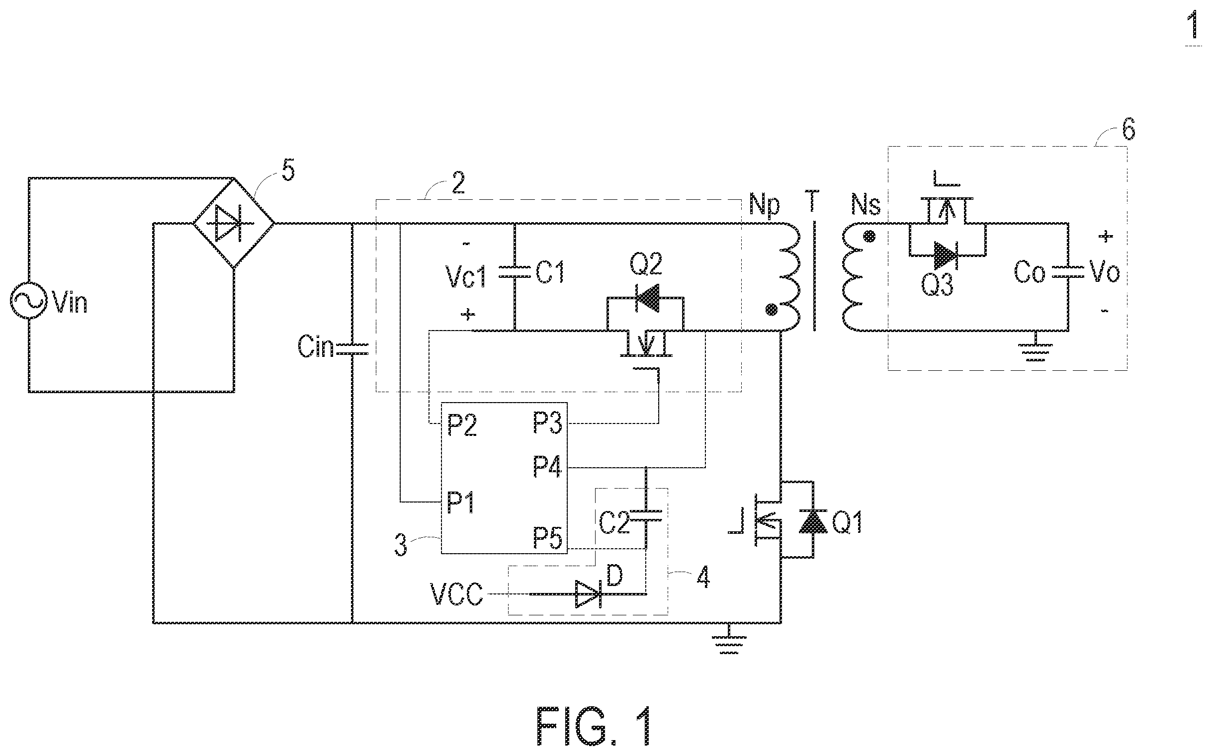
The present disclosure will now be described more specifically with reference to the following embodiments. It is to be noted that the following descriptions of preferred embodiments of this disclosure are presented herein for purpose of illustration and description only. It is not intended to be exhaustive or to be limited to the precise form disclosed. Please refer to . is a schematic circuit diagram illustrating the circuitry topology of a flyback power converter according to a first embodiment of the present disclosure. is a schematic timing waveform diagram illustrating associated signals of the flyback power converter as shown in . The flyback power converter 1 receives an AC input voltage Vin. By the flyback power converter 1 , the AC input voltage Vin is converted into a DC output voltage Vo. In an embodiment, the flyback power converter 1 includes a transformer T, a voltage clamping circuit 2 , a main switch element Q 1 and a control circuit 3 . The voltage clamping circuit 2 includes a first capacitor C 1 and a clamping switch element Q 2 . The first capacitor C 1 includes a first terminal and a second terminal. The clamping switch element Q 2 includes a first terminal, a second terminal and a control terminal. The second terminal of the clamping switch element Q 2 is electrically connected with the second terminal of the first capacitor C 1 . The transformer T includes a primary winding Np and a secondary winding Ns, which are magnetically coupled with each other. The primary winding Np includes a first terminal and a second terminal. The first terminal of the primary winding Np is electrically connected with the first terminal of the first capacitor C 1 . The second terminal of the primary winding Np is electrically connected with the first terminal of the clamping switch element Q 2 . The main switch element Q 1 includes a control terminal, a first terminal and a second terminal. The first terminal of the main switch element Q 1 is electrically connected with the first terminal of the clamping switch element Q 2 and the second terminal of primary winding Np. The second terminal of the main switch element Q 1 is connected to the ground terminal. The control terminal of the main switch element Q 1 is electrically connected with a main controller (not shown). The on/off states of the main switch element Q 1 are controlled by the main controller. The first terminal of the first capacitor C 1 , the second terminal of the first capacitor C 1 , the control terminal of the clamping switch element Q 2 and the first terminal of the clamping switch element Q 2 are electrically connected with the control circuit 3 . A reference voltage Vref and a reference current value Iref are previously stored in the control circuit 3 . There is a capacitor voltage Vc 1 between the second terminal and the first terminal of the first capacitor C 1 . The control circuit 3 receives the capacitor voltage Vc 1 . Moreover, the voltage of the first capacitor C 1 at the second terminal is greater than the voltage of the first capacitor C 1 at the first terminal. That is, the first terminal of the first capacitor C 1 is a negative terminal, and the second terminal of the first capacitor C 1 is a positive terminal. In addition, the value of the capacitor voltage Vc 1 is not negative. The control circuit 3 further receives the current flowing through the clamping switch element Q 2 . The direction of the current flowing from the first terminal of the clamping switch element Q 2 to the second terminal of the clamping switch element Q 2 is defined as a forward direction (i.e., a positive direction). It is noted that the method of detecting the current value of the current flowing through the clamping switch element Q 2 is not restricted. For example, a Hall current sensor or a sampling resistor may be used to detect the current value. Alternatively, the current value may be detected according to the voltage drop of the clamping switch element Q 2 . The current flowing through the clamping switch element Q 2 is denoted as IQ 2 . The current IQ 2 is obtained according to the voltage from the first terminal to the second terminal of the clamping switch element Q 2 . The control circuit 3 compares the capacitor voltage Vc 1 with the reference voltage Vref. According to the comparing result, the on state of the clamping switch element Q 2 is correspondingly controlled. Moreover, the control circuit 3 compares the current IQ 2 with the reference current value Iref. According to the comparing result, the off state of the clamping switch element Q 2 is correspondingly controlled. In an embodiment, the main switch element Q 1 and the clamping switch element Q 2 are N-type MOSFET transistors. In each of the main switch element Q 1 and the clamping switch element Q 2 , the control terminal is the gate terminal, the first terminal is the drain terminal, and the second terminal is the source terminal. Moreover, the gate-source charge (Qgs) of the clamping switch element Q 2 is lower than 10 nC, and the reverse recovery time of the body diode is lower than 100 ns. In an embodiment, the flyback power converter 1 further includes a rectifying circuit 5 , an input capacitor Cin and a secondary circuit 6 . The rectifying circuit 5 receives and rectifies the input voltage Vin. The first terminal of the input capacitor Cin is electrically connected with the rectifying circuit 5 (or a first input terminal) and the first terminal of the transformer T. The second terminal of the input capacitor Cin is connected with the ground terminal (or a second input terminal). The input capacitor Cin is used for voltage stabilization. The secondary circuit 6 is electrically connected with the secondary winding Ns of the transformer T. The electric power from the secondary winding Ns is converted by the secondary circuit 6 . Consequently, the output voltage Vo is generated and outputted from the flyback power converter 1 . In an embodiment, the secondary circuit 6 includes a third switch element Q 3 and an output capacitor Co. The third switch element Q 3 is electrically connected between the first terminal of the secondary winding Ns and the first terminal of the output capacitor Co. The second terminal of the output capacitor Co is connected with the ground terminal. The first terminal and the second terminal of the output capacitor Co are formed as the output terminal of the flyback power converter 1 to output the output voltage Vo. Hereinafter, the operations of the flyback power converter 1 will be described with reference to . In the time interval between the time point t 0 and the time point t 1 , the driving voltage Vg_Q 1 provided to the control terminal of the main switch element Q 1 is switched from a high-level state to a low-level state. Consequently, the main switch element Q 1 is switched from the on state to the off state. Moreover, the drain-source voltage Vds_Q 1 between the first terminal and the second terminal of the main switch element Q 1 is gradually increased. Meanwhile, the capacitor voltage Vc 1 is lower than the reference voltage Vref. Consequently, the driving voltage Vg_Q 2 provided to the control terminal of the clamping switch element Q 2 is in the low-level state under control of the control circuit 3 . In addition, the clamping switch Q 2 is in the off state. Moreover, at the time point t 1 , the condition of turning on the body diode of the clamping switch element Q 2 is satisfied. In the time interval between time point t 1 and the time point t 2 , the capacitor value Vc 1 is still lower than the reference voltage Vref. Consequently, the clamping switch element Q 2 is turned off. Meanwhile, the leakage inductance energy of the transformer T is transferred through the body diode of the clamping switch element Q 2 and recycled to the first capacitor C 1 to charge the first capacitor C 1 . At the time point t 2 , the capacitor voltage Vc 1 is equal to the reference voltage Vref. Meanwhile, the driving voltage Vg_Q 2 provided to the control terminal of the clamping switch element Q 2 is switched from the low-level state to the high-level state. Consequently, the clamping switch element Q 2 is switched from the off state to the on state. In the time interval between the time point t 2 and the time point t 3 , the current IQ 2 flows in the direction from the first terminal of the clamping switch element Q 2 to the second terminal of the clamping switch element Q 2 . That is, the current IQ 2 flows in the forward direction. Meanwhile, the first capacitor C 1 is charged by the leakage inductance energy from the transformer T. At the time point t 3 , the current IQ 2 flowing through the clamping switch element Q 2 is zero, and the capacitor voltage Vc 1 of the capacitor C 1 reaches the maximum value. Since the capacitor voltage Vc 1 is greater than the reference voltage Vref, the clamping switch element Q 2 is still turned on under control of the control circuit 3 . In the time interval between the time point t 3 and the time point t 4 , the current IQ 2 flows in the direction from the second terminal of the clamping switch element Q 2 to the first terminal of the clamping switch element Q 2 . That is, the current IQ 2 flows through the clamping switch element Q 2 in a reverse direction (or a negative direction). The value of the current IQ 2 received by the control circuit 3 is negative. Meanwhile, the stored energy in the first capacitor C 1 is discharged through the channel region of the second switch element Q 2 . Consequently, the capacitor voltage Vc 1 is gradually decreased. In addition, the energy is transferred to the secondary side of the transformer T. That is, the stored energy discharged from the first capacitor C 1 is transferred to the leakage inductor of the transformer T and the output terminal of the flyback power converter 1 . At the time point t 4 , the capacitor voltage Vc 1 is lower than the reference voltage Vref, and the current IQ 2 received by the clamping switch element Q 2 is equal to the reference current value Iref. Meanwhile, the clamping switch element Q 2 is switched from the on state to the off state under control of the control circuit 3 . Since the energy in the first capacitor C 1 is discharged through the clamping switch element Q 2 , no reverse recovery process of the diode occurs. Since the reverse recovery process of the diode does not occur, the reverse recovery loss of the diode is reduced, and the efficiency of the flyback power converter 1 is enhanced. In addition, a greater portion of the leakage inductance is recycled. When compared with the flyback power converter using the active clamp flyback (ACF) control method, the control method of the flyback power converter 1 is simplified and the control mechanism is more cost-effective. In addition, the risk of isolation failure between the primary and secondary sides of the transformer T is avoided when the clamping switch element Q 2 is turned on once only. Furthermore, in case that the voltage stress of the main switch element Q 1 does not exceed the allowable voltage stress, the magnitude of the reference voltage Vref may be set as a higher value. In other words, after plural switching cycles of the main switch element Q 1 , the clamping switch circuit Q 2 enters the switching state. Consequently, the working frequency of the voltage clamping circuit 2 is reduced, and the efficiency of recovering the leakage inductance energy recovery is enhanced. The associated principle will be described with reference to . is a schematic timing waveform diagram illustrating associated signals of the flyback power converter as shown in , in which the reference voltage is set at a higher value. The time interval between the time point t 0 and the time point t 1 is a switching cycle. In the switching cycle, the capacitor voltage Vc 1 is lower than the reference voltage Vref. Under this circumstance, the clamping switch element Q 2 is maintained in the off state, and the leakage inductance energy is transferred through the body diode of the clamping switch element Q 2 and stored in the first capacitor C 1 . In the switching cycle between the time point t 1 and the time point t 2 and the switching cycle between the time point t 2 and the time point t 3 , the capacitor voltage Vc 1 is also lower than the reference voltage Vref, and the clamping switch element Q 2 is maintained in the off state. At the time point t 4 , the capacitor voltage Vc 1 reaches the reference voltage Vref. Consequently, under control of the control circuit 3 , the clamping switch element Q 2 is turned on. At the time point t 5 , the capacitor voltage Vc 1 is lower than the reference voltage Vref, and the current IQ 2 flowing through the clamping switch element Q 2 reaches the reference current value Iref. Meanwhile, the clamping switch element Q 2 is turned off under control of the control circuit 3 . Consequently, the capacitor voltage Vc 1 is restored to the initial value corresponding to the time point t 0 . In an embodiment, the voltage specifications of the main switch element Q 1 and the clamping switch element Q 2 are identical. The on-resistance of the main switch element Q 1 is at the mohm level, and the on-resistance of the clamping switch element Q 2 is at the ohm level. Consequently, the switching speed of the clamping switch element Q 2 is faster, and the conduction time of the body diode of the clamping switch element Q 2 is reduced. Especially, the reference voltage Vref is greater than the product of the transformation ratio of the transformer T and the output voltage Vo of the flyback power converter 1 . In addition, the reference voltage Vref is less than 1.5 times the product of the transformation ratio of the transformer T and the output voltage Vo of the flyback power converter 1 . The input voltage Vin of the flyback power converter 1 is AC current, and the input voltage Vin is in the range between 90 Vac and 264 Vac. The transformation ratio of the transformer T is 6:1, the leakage inductance of the transformer T is 5.4 uH, the working frequency is 60 kHZ, the output voltage Vo is 20V, and the capacitance of the first capacitor C 1 is 1˜4.7 nF. The reference voltage Vref is set as Vo×(the turn ratio of the transformer T)×(1˜1.5). For example, the reference voltage Vref is set as 140V. The reference current value Iref is set as zero or a negative value. For example, the reference current value Iref is set according to the voltage drop of the clamping switch element Q 2 when the current flowing through the on-state clamping switch element Q 2 is −1 A. It is noted that the above parameters are not restricted. That is, the parameters of the flyback power converter 1 may be varied according to the practical requirements. In an embodiment, the control circuit 3 is an IC chip with five pins. The five pins include a first pin P 1 , a second pin P 2 , a third pin P 3 , a fourth pin P 4 and a fifth pin P 5 . The first pin P 1 is electrically connected with the first terminal of the first capacitor C 1 . The second pin P 2 is electrically connected with the second terminal of the first capacitor C 1 . The third pin P 3 is electrically connected with the control terminal of the clamping switch element Q 2 . The fourth pin P 4 is electrically connected with the first terminal of the clamping switch element Q 2 . The voltages from the first terminal and the second terminal of the first capacitor C 1 are respectively received by the first pin P 1 and the second pin P 2 . The fourth pin P 4 and the second pin P 2 are used to detect the current IQ 2 flowing through the clamping switch element Q 2 . By detecting the voltage drop across the clamping switch element Q 2 , the purpose of detecting the current signal can be achieved. In an embodiment, the flyback power converter 1 further includes a bootstrap circuit 4 . The bootstrap circuit 4 is electrically connected with the fourth pin P 4 and the fifth pin P 5 of the control circuit 3 to provide electric power to the control circuit 3 . The bootstrap circuit 4 includes a diode D and a bootstrap capacitor C 2 . The anode of the diode D is electrically connected with a voltage source VCC. The cathode of the diode D is electrically connected with the first terminal of the bootstrap capacitor C 2 and the fifth pin P 5 of the control circuit 3 . The second terminal of the bootstrap capacitor C 2 is electrically connected with the first pin P 1 of the control circuit 3 and the first terminal of the main switch element Q 1 . When the first switch element Q 1 is turned on, the fourth pin P 4 is connected to the ground terminal, and the voltage source VCC is transmitted through the diode D to charge the fifth pin P 5 of the control circuit 3 . When the first switch element Q 1 is turned off, the stored energy in the fifth pin P 5 of the control circuit 3 provides a driving signal to the clamping switch element Q 2 . Please refer to , 2 , 3 and 4 . is a flowchart illustrating a control method for the flyback power converter according to an embodiment of the present disclosure. The control method is applied to the flyback power converter 1 as shown in . As shown in , the control method includes the following steps. In a step S 1 , the flyback power converter 1 as shown in is provided. In a step S 2 , the capacitor voltage Vc 1 between the second terminal and the first terminal of the first capacitor C 1 and the current IQ 2 flowing through the clamping switch element Q 2 are detected by the control circuit 3 . In a step S 3 , the control circuit 3 receives the capacitor voltage Vc 1 . The first terminal of the first capacitor C 1 is the negative terminal. The second terminal of the first capacitor C 1 is the positive terminal. The capacitor voltage Vc 1 is not negative. Moreover, the control circuit 3 determines whether the capacitor voltage Vc 1 is greater than the reference voltage Vref. If the determining result of the step S 3 is satisfied, a step S 4 is conducted. Whereas, if the determining result of the step S 3 is not satisfied, the control method returns to conduct the step S 2 again. In the step S 4 , the clamping switch element Q 2 is turned on under control of the control circuit 3 . In addition, the control circuit 3 determines whether the capacitor voltage Vc 1 is lower than or equal to the reference voltage Vref. If the determining result of the step S 4 is satisfied, a step S 5 is conducted. Whereas, if the determining result of the step S 4 is not satisfied, the step S 4 is conducted again. In the step S 5 , the control circuit 3 determines whether the current IQ 2 is lower than the reference current value Iref. If the determining result of the step S 5 is satisfied, a step S 6 is conducted. Whereas, if the determining result of the step S 5 is not satisfied, the control method returns to conduct the step S 4 again. In the step S 6 , the clamping switch element Q 2 is turned off under control of the control circuit 3 . From the above descriptions, the present disclosure provides a flyback power converter and a control method for the flyback power converter. The diode used in the RCD clamping circuit is replaced by the clamping switch element of the flyback power converter. The on/off states of the clamping switch element in the voltage clamping circuit are controlled according to the capacitor voltage of the first capacitor and the current flowing through the clamping switch element. Since the reverse recovery process of the diode does not occur, the reverse recovery loss of the diode is reduced, and the efficiency of the flyback power converter is enhanced. When compared with the flyback power converter using the active clamp flyback (ACF) control method, the control method of the flyback power converter is simplified. In addition, the risk of isolation failure between the primary and secondary sides of the transformer is avoided. While the disclosure has been described in terms of what is presently considered to be the most practical and preferred embodiments, it is to be understood that the disclosure needs not be limited to the disclosed embodiment. On the contrary, it is intended to cover various modifications and similar arrangements included within the spirit and scope of the appended claims which are to be accorded with the broadest interpretation so as to encompass all such modifications and similar structures.
Figures (4)
Citations
This patent cites (11)
- US10103616
- US2014/0185333
- US2015/0131341
- US2017/0176919
- US2018/0062529
- US2019/0013739
- US2019/0356232
- US2021/0313897
- US110677045
- US113410994
- US112003476