Data Latch Circuit and Semiconductor Storage Device
Abstract
A data latch circuit includes a first transistor of a first conductivity type and a second transistor of the first conductivity type, and a third transistor of a second conductivity type and a fourth transistor of the second conductivity type. The third and fourth transistors are controlled to perform a first control operation to store data in the data latch circuit and to perform a second control operation to read the stored data.
Claims (10)
1 . A data latch circuit comprising: a first transistor of a first conductivity type and a second transistor of the first conductivity type; and a third transistor of a second conductivity type and a fourth transistor of the second conductivity type, wherein a source of the first transistor and a source of the second transistor are connected to a predetermined first reference voltage node, a source of the third transistor is connected to a drain of the first transistor and a gate of the second transistor, a source of the fourth transistor is connected to a drain of the second transistor and a gate of the first transistor, a data wiring layer is connected to a drain of the third transistor and a drain of the fourth transistor, a first gate layer is connected to a gate of the third transistor and not connected to the gate of the first transistor, a second gate layer is connected to a gate of the fourth transistor and not connected to the gate of the second transistor, and the third and fourth transistors are controlled according to a first control signal supplied to the first gate layer and a second control signal supplied to the second gate layer, respectively, to perform a first control operation to store data corresponding to a voltage applied to the data wiring layer in the data latch circuit and to perform a second control operation to read the stored data.
5 . A data latch circuit comprising: a first transistor of a first conductivity type and a second transistor of the first conductivity type; a third transistor of a second conductivity type and a fourth transistor of the second conductivity type; a first gate layer connected to a gate of the third transistor and a gate of the fourth transistor; a first data wiring layer connected to a drain of the third transistor; and a second data wiring layer connected to a drain of the fourth transistor, wherein a source of the first transistor and a source of the second transistor are connected to a predetermined first reference voltage node, a source of the third transistor is connected to a drain of the first transistor and a gate of the second transistor, a source of the fourth transistor is connected to a drain of the second transistor and a gate of the first transistor, the third and fourth transistors are controlled according to a control signal through the first gate layer to perform a first control operation to store data corresponding to voltages applied to the first and second data wiring layers in the data latch circuit and to perform a second control operation to read the stored data.
9 . A semiconductor storage device comprising: a memory cell array having a bit line and first and second word lines; and a data latch circuit configured to temporarily store data to be written to the memory cell array and the data read from the memory cell array, wherein the data latch circuit comprises: a data storage circuit including at least two, but no more than four transistors of a first conductivity type, the at least two transistors of the first conductivity type including first and second transistors, and third and fourth transistors of a second conductivity type, and further wherein a source of the first transistor and a source of the second transistor are connected to a predetermined first reference voltage node, a source of the third transistor is connected to a drain of the first transistor and a gate of the second transistor, a source of the fourth transistor is connected to a drain of the second transistor and a gate of the first transistor, a data wiring layer is connected to the bit line, a drain of the third transistor, and a drain of the fourth transistor, a first gate layer is connected to the first word line and a gate of the third transistor, a second gate layer is connected to the second word line and a gate of the fourth transistor, and the third and fourth transistors are controlled according to a first control signal supplied to the first gate layer and a second control signal supplied to the second gate layer, respectively, to perform a first control operation to store data corresponding to a voltage applied to the data wiring layer in the data latch circuit and to perform a second control operation to read the stored data.
Show 7 dependent claims
2 . The data latch circuit according to claim 1 , wherein voltage levels of the first gate layer and the second gate layer in a period during which the data is retained are lowered by any percentage in a range of 5 to 30% of uppermost voltage levels of the first gate layer and the second gate layer when the data is written.
3 . The data latch circuit according to claim 2 , further comprising: first and second diffusion regions that are located apart from each other in a first direction on a semiconductor substrate; a third gate layer connected to the gate of the first transistor; and a fourth gate layer connected to the gate of the second transistor, wherein: source and drain of each of the first transistor and the second transistor are located on the first diffusion region, source and drain of each of the third transistor and the fourth transistor are located on the second diffusion region, the first gate layer and the second gate layer extend in a second direction intersecting the first direction so as to overlap the second diffusion region in a stacking direction, the data wiring layer extends in the first direction so as to overlap the first diffusion region and the second diffusion region in the stacking direction, and the third gate layer and the fourth gate layer extend in the second direction, respectively, so as to overlap the first diffusion region in the stacking direction, and are located apart from each other in the first direction.
4 . The data latch circuit according to claim 2 , further comprising: first, second, third, and fourth diffusion regions, that are located apart from each other in a second direction intersecting a first direction on a semiconductor substrate; a third gate layer connected to the gate of the first transistor; and a fourth gate layer connected to the gate of the second transistor, wherein: the first, second, third, and fourth gate layers extend in the first direction, respectively, and are located apart from each other in the second direction, and the data wiring layer is located between the second diffusion region and the third diffusion region and extends in the first direction.
6 . The data latch circuit according to claim 5 , wherein a voltage level of the first gate layer in a period during which the data is retained in the data latch circuit is lowered by any percentage in a range of 5 to 30% of a power supply voltage level.
7 . The data latch circuit according to claim 6 , further comprising: first and second diffusion regions that are located apart from each other in a second direction intersecting a first direction on a semiconductor substrate; a third diffusion region located apart from the first diffusion region and the second diffusion region in the first direction; a second gate layer connected to the gate of the first transistor; and a third gate layer connected to the gate of the second transistor, wherein source and drain of the first transistor are located on the first diffusion region, source and drain of the second transistor are located on the second diffusion region, source and drain of each of the third transistor and the fourth transistor are located on the third diffusion region, the first gate layer extends in the second direction so as to overlap the first diffusion region and the second diffusion region in the stacking direction, the second gate layer and the third gate layer extend in the second direction, respectively, so as to overlap the third diffusion region in the stacking direction, and are located apart from each other in the first direction, the first data wiring layer extends in the first direction so as to overlap the first diffusion region and the third diffusion region in the stacking direction, and the second data wiring layer extends in the first direction so as to overlap the second diffusion region and the third diffusion region in the stacking direction.
8 . The data latch circuit according to claim 6 , further comprising: first, second, third, and fourth diffusion regions, that are located apart from each other in a second direction intersecting a first direction on a semiconductor substrate; a first gate layer connected to the gate of the third transistor; a second gate layer connected to the gate of the fourth transistor; a third gate layer connected to the gate of the first transistor; and a fourth gate layer connected to the gate of the second transistor, wherein: source and drain of the first transistor are located on the first diffusion region, source and drain of the second transistor are located on the fourth diffusion region, source and drain of the third transistor are located on the second diffusion region, source and drain of the fourth transistor are located on the third diffusion region, the first data wiring layer extends in the first direction so as to overlap the second diffusion region in the stacking direction, and the second data wiring layer extends in the first direction so as to overlap the third diffusion region in the stacking direction.
10 . The semiconductor storage device according to claim 9 , wherein the data storage circuit includes four transistors of the first conductivity type.
Full Description
Show full text →
CROSS-REFERENCE TO RELATED APPLICATION
This application is based upon and claims the benefit of priority from Japanese Patent Application No. 2021-204613, filed Dec. 16, 2021, the entire contents of which are incorporated herein by reference. FIELD Embodiments described herein relate generally to a data latch circuit and a semiconductor storage device.
BACKGROUND
Bit density of flash memory continuously increases by the use of multi-level cells (MLCs) and three-dimensional stacking. As the bit density thereof increases, the area of peripheral circuits also increases. Among the peripheral circuits, a data latch circuit (also referred to as a page buffer) occupies the largest area. When the data latch circuit cannot be made smaller, it becomes difficult to reduce the size of the flash memory chip. DESCRIPTION OF THE DRAWINGS is a block diagram showing a schematic configuration of a semiconductor storage device including a data latch circuit according to a first embodiment. is a circuit diagram of a data latch circuit according to a comparative example. A is a diagram showing characteristics of the data latch circuit according to the first embodiment. B is a circuit diagram of the data latch circuit according to the first embodiment. A is a diagram showing operation of the data latch circuit according to the first embodiment. B is a diagram showing voltage of a word line and a bit line when the data latch circuit in A reads data, writes the same, and stores the same. is a diagram showing storage characteristics of the semiconductor storage device according to the first embodiment. is a layout diagram of the data latch circuit according to the first embodiment. is a cross-sectional view showing a stacking position of each layer in . is a layout diagram in which a plurality of data latch circuits having layout arrangement in are located in a two-dimensional direction. A is a layout diagram of a first modification of the data latch circuit according to the first embodiment. B is a diagram showing a configuration in which layout arrangement in A is shifted to the left or right by a half cycle. A is a layout diagram in which a plurality of data latch circuits having the layout arrangement in A are located in a first direction and a second direction. B is a layout diagram in which a plurality of data latch circuits having layout arrangement in B are located in the first direction and the second direction. A is a diagram showing characteristics of a data latch circuit according to a second embodiment. B is a circuit diagram of the data latch circuit according to the second embodiment. C is a diagram showing voltage of a word line and a bit line when the data latch circuit in B reads data, writes the same, and stores the same. is a layout diagram of the data latch circuit according to the second embodiment. is a layout diagram in which a plurality of data latch circuits having layout arrangement in are located in the two-dimensional direction. A is a layout diagram of a first modification of the data latch circuit according to the second embodiment. B is a layout diagram of a second modification. A is a layout diagram in which a plurality of data latch circuits having layout arrangement in A are located in the first direction and the second direction. B is a layout diagram in which a plurality of data latch circuits having layout arrangement shown in B are located in the first direction and the second direction. A is a diagram showing characteristics of a data latch circuit according to a third embodiment. B is a circuit diagram of the data latch circuit according to the third embodiment. C is a diagram showing voltage of a word line, a bit line, and a control signal when the data latch circuit in B reads data, writes the same, and stores the same. is a layout diagram of the data latch circuit according to the third embodiment. is a layout diagram in which a plurality of data latch circuits having layout arrangement in are located in the two-dimensional direction. A is a diagram showing characteristics of a data latch circuit according to a fourth embodiment. B is a circuit diagram of the data latch circuit according to the fourth embodiment. C is a diagram showing voltage of a word line, a bit line, and a control signal when the data latch circuit in B reads data, writes the same, and stores the same. is a layout diagram of the data latch circuit according to the fourth embodiment. is a layout diagram in which a plurality of data latch circuits having layout arrangement in are located in the two-dimensional direction.
DETAILED DESCRIPTION
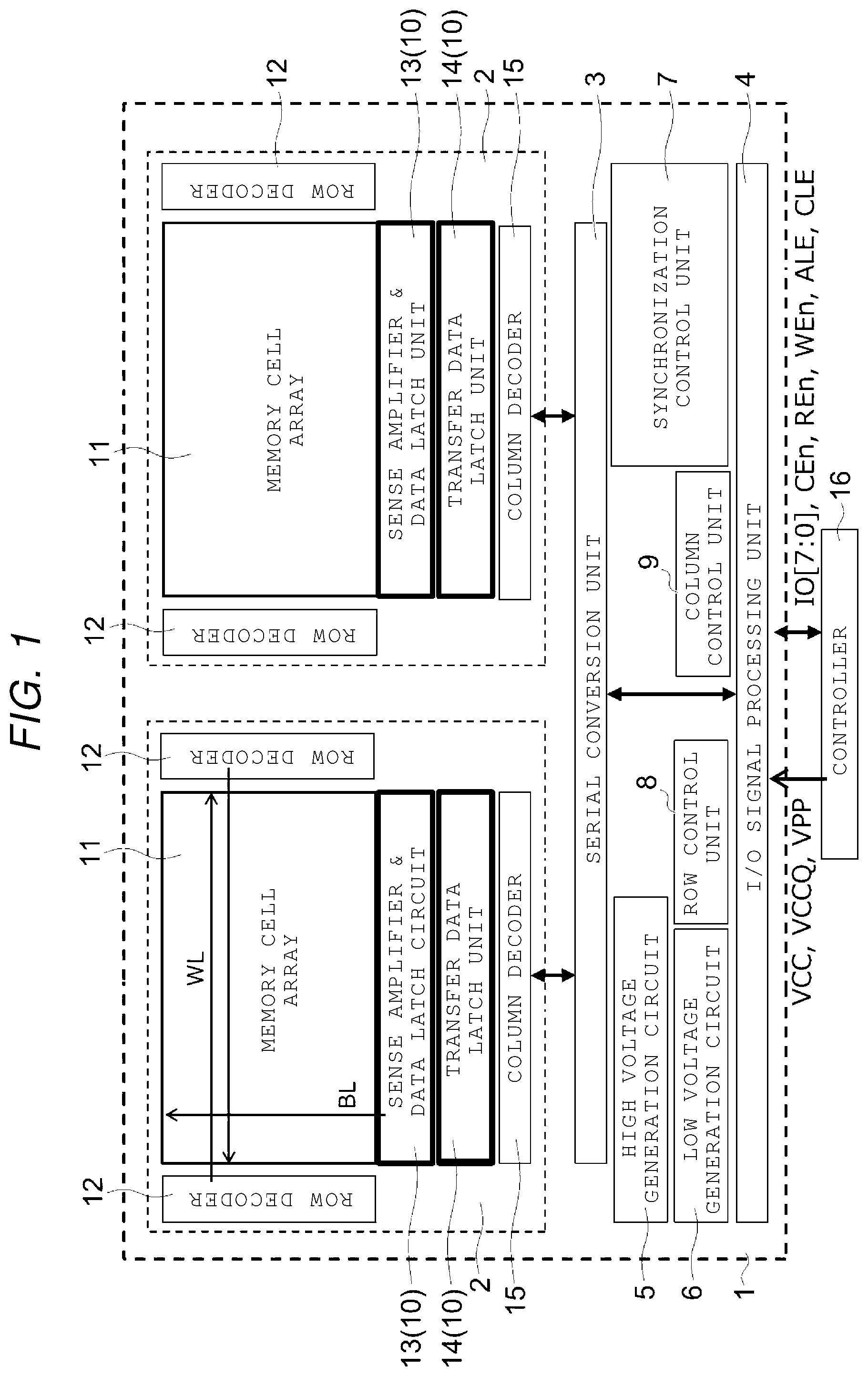
Embodiments provide a data latch circuit and a semiconductor storage device capable of being miniaturized. In general, according to one embodiment, a data latch circuit includes a first transistor of a first conductivity type and a second transistor of the first conductivity type, and a third transistor of a second conductivity type and a fourth transistor of the second conductivity type. The third and fourth transistors are controlled to perform a first control operation to store data in the data latch circuit and to perform a second control operation to read the stored data. Hereinafter, embodiments of a data latch circuit and a semiconductor storage device will be described with reference to the drawings. In the following description, main components of the data latch circuit and the semiconductor storage device will be mainly described. The data latch circuit and the semiconductor storage device may have components and functions not shown in the drawings or not described in this specification. The following description is not intended to exclude the components or the functions not shown in the drawings or not described in this specification. First Embodiment is a block diagram showing a schematic configuration of a semiconductor storage device 1 including a data latch circuit 10 according to a first embodiment. The semiconductor storage device 1 in shows a schematic configuration of flash memory. The semiconductor storage device 1 according to the embodiment is applicable to various types of semiconductor memory other than the flash memory. More specifically, the semiconductor storage device 1 according to the embodiment is applicable to a nonvolatile memory such as MRAM (Magnetoresistive Random Access Memory) and is also applicable to volatile memory such as DRAM (Dynamic Random Access Memory) and SRAM (Static Random Access Memory). Additionally, the flash memory may be a NAND flash memory or a NOR flash memory, and the semiconductor storage device 1 according to the embodiment is applicable to both the NAND flash memory and the NOR flash memory. In the following description, an example in which the semiconductor storage device 1 according to the embodiment is applied to the flash memory will be mainly described. The semiconductor storage device 1 in includes a plurality of memory modules 2 , a serial conversion unit 3 , an I/O signal processing unit 4 , a high voltage generation circuit 5 , a low voltage generation circuit 6 , a synchronization control unit 7 , a row control unit 8 , and a column control unit 9 . Each of the memory modules 2 includes a memory cell array 11 , a row decoder 12 , a sense amplifier & data latch unit 13 , a transfer data latch unit 14 , and a column decoder 15 . The memory cell array 11 has a configuration in which a plurality of strings, having a plurality of NAND flash memory cells provided therein in the form of a cascode connection, are located in a two-dimensional configuration. The row decoder 12 decodes a row address signal and drives a corresponding word line. The sense amplifier & data latch unit 13 writes data to the memory cell array 11 and reads the data from the memory cell array 11 via a bit line BL. The sense amplifier & data latch unit 13 includes the data latch circuit (DL) 10 , according to the embodiment, which is configured to store the data to be written to the memory cell array 11 and to store the data read from the memory cell array 11 . The transfer data latch unit 14 temporarily stores the data to be written to the memory cell array 11 or the data read from the memory cell array 11 . The transfer data latch unit 14 also includes the data latch circuit 10 according to the embodiment. The column decoder 15 performs predetermined operation processing including decoding processing for the data to be written to the memory cell array 11 or the data to be read from the memory cell array 11 . The serial conversion unit 3 converts the data read from the memory cell array 11 into serial data, and supplies the converted data to the I/O signal processing unit 4 . Further, the serial conversion unit 3 converts the serial data to be written, transmitted from the I/O signal processing unit 4 , into parallel data and sends the same to the column decoder 15 . The I/O signal processing unit 4 performs high-speed serial communication with a controller 16 . The high voltage generation circuit 5 boosts power supply voltage VDD supplied from the outside, thereby generating high-voltage VPGM, VERA, VPASS, and the like to be used when data is written to or erased from the memory cell. The low voltage generation circuit 6 generates a reference voltage, a clock signal, a low power supply voltage, and the like to be used in the semiconductor storage device 1 . The synchronization control unit 7 performs timing control, sequence control, parameter control for each block in the semiconductor storage device 1 . The row control unit 8 controls the timing of driving a word line in each memory cell array 11 . The column control unit 9 controls the timing of driving a bit line in each memory cell array 11 . As described above, the data latch circuit 10 according to the embodiment is provided in the sense amplifier & data latch unit 13 and the transfer data latch unit 14 in the semiconductor storage device 1 in . The data latch circuit 10 according to the embodiment may be provided in a place other than the sense amplifier & data latch unit 13 and the transfer data latch unit 14 . The flash memory having the block configuration shown in is currently the lowest cost non-volatile memory, and is generally used as a large-capacity storage in various applications. In the block configuration shown in , components other than the memory cell array 11 may be referred to as peripheral circuits. The data latch circuit 10 occupies most of the area of the peripheral circuits. The data latch circuit 10 , which is used as a temporary storage place, is configured to temporarily store the data to be written to the memory cell array 11 and the data read from the same. In the flash memory configured to change from a planar structure to a three-dimensional structure, the bit density thereof is improved by increasing the number of bits per cell, implementing a multi-level cell (MLC), and increasing the number of stacked word lines. Here, as the bit density thereof increases, the area of the peripheral circuit increases. When the ratio of the area of the peripheral circuit to the total area of the flash memory chip becomes large, the number of bits per wafer is reduced, and bit costs increase. As a solution to reduce the area of the flash memory chip, proposed are a CUA (CMOS Under Array) structure, in which the peripheral circuit is disposed below the memory cell array 11 , and a CBA (CMOS Bonded Array) structure, in which a wafer having the memory cell array 11 disposed thereon and a wafer having the peripheral circuit disposed thereon are bonded together. In both the CUA structure and the CBA structure, when the area of the peripheral circuit is larger than that of the memory cell array 11 , the area of the flash memory chip increases. Therefore, the semiconductor storage device 1 according to the embodiment is characterized in that the area of the data latch circuit 10 in the peripheral circuit is reduced. Hereinafter, first, a circuit configuration of a general-purpose data latch circuit 100 according to a comparative example will be described. is a circuit diagram of the data latch circuit 100 according to the comparative example. The data latch circuit 100 in includes eight transistors Q 1 to Q 8 . Among the eight transistors Q 1 to Q 8 , four transistors are referred to as NMOS transistors Q 1 to Q 4 , and the remaining four transistors are referred to as PMOS transistors Q 5 to Q 8 . A drain of the transistor Q 1 is connected to a gate of the transistor Q 2 , a drain of the transistor Q 3 , a drain of the transistor Q 7 , and a gate of the transistor Q 8 . A drain of the transistor Q 2 is connected to a gate of the transistor Q 1 , a drain of the transistor Q 4 , a gate of the transistor Q 7 , and a drain of the transistor Q 8 . Sources of the transistors Q 1 and Q 2 are connected to a reference voltage VSS node (for example, a ground node). A word line WL 1 is connected to a gate of the transistor Q 3 , and a word line WL 2 is connected to a gate of the transistor Q 4 . Only one of the word lines WL 1 and WL 2 goes to a high level. Sources of the transistors Q 3 and Q 4 are connected to a bit line BL. In this manner, the data latch circuit 100 in includes two word lines WL 1 and WL 2 and one bit line BL. A source of the transistor Q 5 is connected to a power supply voltage VDD node, a drain of the transistor Q 5 is connected to a source of the transistor Q 7 , and a control signal Vctl is input to a gate of the transistor Q 5 . A source of the transistor Q 6 is connected to the power supply voltage VDD node, a drain of the transistor Q 6 is connected to a source of the transistor Q 8 , and a control signal Vctl is input to the gate of the transistor Q 7 . When the control signal Vctl is a low level, both the transistors Q 5 and Q 6 are turned ON. In this case, when either the word line WL 1 or the WL 2 goes to a high level, the nodes n 1 and n 2 store the data on the bit line BL. As shown in , the data latch circuit 100 according to the comparative example is formed of eight transistors Q 1 to Q 8 . Accordingly, as the number of data latch circuits 100 increases, the number of transistors increases by a multiple of 8, which results in increasing the area of the semiconductor storage device 1 . A is a diagram showing characteristics of the data latch circuit 10 according to the first embodiment, and B is a circuit diagram of the data latch circuit 10 according to the first embodiment. As shown in A , the data latch circuit 10 according to the first embodiment has a configuration in which a first transistor group 21 including the transistors Q 5 and Q 6 , a second transistor group 22 including the transistors Q 7 and Q 8 , and VDD are omitted from the data latch circuit 100 according to the comparative example of . Further, the data latch circuit 10 according to the first embodiment includes PMOS transistors Q 3 a and Q 4 a instead of the NMOS transistors Q 3 and Q 4 in . As described above, the data latch circuit 10 according to the first embodiment includes two NMOS transistors Q 1 and Q 2 and two PMOS transistors Q 3 a and Q 4 a. As shown in B , the drain of the transistor Q 1 is connected to the gate of the transistor Q 2 and a source of the transistor Q 3 a . This connection node is referred to as a node n 1 . The drain of the transistor Q 2 is connected to the gate of the transistor Q 1 and a source of the transistor Q 4 a . This connection node is referred to as a node n 2 . The sources of the transistors Q 1 and Q 2 are connected to the ground node. A gate of the transistor Q 3 a is connected to the word line WL 1 and a gate of the transistor Q 4 a is connected to the word line WL 2 . The drains of the transistors Q 3 a and Q 4 a are connected to the bit line. A is a diagram showing operation of the data latch circuit 10 according to the first embodiment. The data latch circuit 10 according to the first embodiment performs data write operation, data storage operation, and data read operation. Two word lines WL 1 and WL 2 do not go to the low level at the same time. When one of the word lines WL 1 and WL 2 goes to the high level, the data write operation is performed. For example, when the word line WL 1 is the low level and the word line WL 2 is the high level, the transistor Q 3 a is turned ON and the transistor Q 4 a is turned OFF. Accordingly, the voltage of the bit line BL is transmitted to the node n 1 via the transistor Q 3 a . For example, when the bit line BL has low voltage, the node n 1 also becomes low voltage, and when the bit line BL has high voltage, the node n 1 also becomes high voltage. The node n 2 becomes inverted logical voltage to the node n 1 . The transistors Q 1 and Q 2 perform operation of storing the voltage of the nodes n 1 and n 2 . In the data storage operation, the two word lines WL 1 and WL 2 are both set to voltage levels slightly lower than the power supply voltage VDD. The bit line BL is set to VDD. The voltage level slightly lower than the power supply voltage VDD is, for example, a voltage level lower than the power supply voltage VDD by 5 to 30%. More specifically, the voltage levels of the gates of the transistors Q 3 a and Q 4 a in a period during which the data is stored in the nodes n 1 and n 2 are lowered by any percentage in a range of 5 to 30% of the high voltage levels of the gates of the transistors Q 3 a and Q 4 a when the data is written to the nodes n 1 and n 2 . The reason for setting the word lines WL 1 and WL 2 to the voltage levels slightly lower than the power supply voltage VDD during the data storage period is to allow leakage current to flow through the transistors Q 3 a and Q 4 a , the gates of which are connected to the word lines WL 1 and WL 2 , respectively. For example, when the node n 1 has the low voltage, the transistor Q 1 is turned ON, and the voltage of the node n 1 is stored at low voltage from the ground voltage VSS node via the transistor Q 1 , as shown by a dashed arrow line y 1 in A . On the other hand, the transistor Q 2 is turned OFF, and the voltage of the node n 2 is stored at high voltage by leakage current flowing from the bit line BL through the transistor Q 4 a , as shown by a dashed arrow line y 2 in A . In this manner, the word lines WL 1 and WL 2 are set to the voltage level slightly lower than the power supply voltage VDD and the bit line BL is set to VDD. Here, when the node n 1 has high voltage, the voltage level of the node n 1 is maintained by leakage current flowing from the bit line BL through the transistor Q 3 a . Further, when the node n 2 has high voltage, the voltage level of the node n 2 is maintained by the leakage current flowing from the bit line BL through the transistor Q 4 a. B is a diagram showing the voltage of the word lines WL 1 and WL 2 , and the bit line BL when the data latch circuit 10 in A reads data, writes the same, and stores the same. B shows an example in which the word line WL 1 is accessed. Here, when the word line WL 2 is accessed, a voltage relationship between the word lines WL 1 and WL 2 in B is reversed. When the data latch circuit 10 reads the data stored in the nodes n 1 and n 2 via the transistor Q 3 a , the word line WL 1 is set to the ground voltage VSS (for example, 0 V) and the word line WL 2 is set to voltage slightly lower than the power supply voltage VDD (for example, VDD×0.95−0.7 V). Further, the bit line BL is pre-charged to the power supply voltage VDD in advance. Accordingly, the data stored in the nodes n 1 and n 2 are read in the bit line BL via the transistor Q 3 a. When the data latch circuit 10 writes the data to the nodes n 1 and n 2 via the transistor Q 3 a , the word line WL 1 is set to the ground voltage VSS (for example, 0 V), and the word line WL 2 is set to the power supply voltage VDD. When the data to be written is 0, the bit line BL is set to the ground voltage VSS (for example, 0 V). Accordingly, the data of “0” is stored in the nodes n 1 and n 2 via the transistor Q 3 a . Meanwhile, when the data to be written is 1, the bit line BL is set to the power supply voltage VDD. When the data latch circuit 10 stores the data in the nodes n 1 and n 2 , the word lines WL 1 and WL 2 are set to voltage slightly lower than the power supply voltage VDD (for example, VDD×0.95−0.7 V), and the bit line BL is set to the power supply voltage VDD. is a diagram showing storage characteristics of the semiconductor storage device 1 according to the first embodiment. A horizontal axis in is the voltage level of the node n 2 , and a vertical axis in is the voltage level of the node n 1 . A curve w 1 in shows a change in the voltage level of the node n 1 with respect to the voltage of the node n 2 , and a curve w 2 shows a change in the voltage level of the node n 2 with respect to the voltage of the node n 1 . As shown in , it can be seen that the nodes n 1 and n 2 are stable at two points p 1 and p 2 and have good storage characteristics. In the point p 1 , the voltage level of the node n 1 is the power supply voltage VDD. In the point p 2 , the voltage level of the node n 2 is the power supply voltage VDD. is a layout diagram of the data latch circuit 10 according to the first embodiment, and is a cross-sectional view showing a stacking position of each layer in . As shown in , the data latch circuit 10 according to the first embodiment is formed by stacking a plurality of layers having different layer heights, and includes a plurality of contacts CT 0 and CT 1 configured to electrically connect the respective layers. shows a planar structure in which the plurality of layers having different layer heights are viewed in the stacking direction. The layout diagram and the cross-sectional view of the data latch circuit 10 according to the first embodiment are not necessarily limited to those shown in . Black and gray circles in represent the contacts. In the examples of , a first diffusion region D 1 and a second diffusion region D 2 are located in the lowest layer. The first diffusion region D 1 and the second diffusion region D 2 may be referred to as active regions. The first diffusion region D 1 and the second diffusion region D 2 are located apart from each other in a first direction X. A source region and a drain region of the transistors Q 1 and Q 2 are formed in the first diffusion region D 1 . A source region and a drain region of the transistors Q 3 a and Q 4 a are formed in the second diffusion region D 2 . The first diffusion region D 1 and the second diffusion region D 2 are formed by implanting impurity ions such as boron (B), phosphorus (P), and arsenic (As) into a semiconductor substrate and thermally diffusing the same therein. A first gate layer G 1 connected to the gate of the transistor Q 3 a and a second gate layer G 2 connected to the gate of the transistor Q 4 a are located on the second diffusion region D 2 via an insulating layer. A third gate layer G 3 connected to the gate of the transistor Q 1 and a fourth gate layer G 4 connected to the gate of the transistor Q 2 are located on the first diffusion region D 1 via an insulating layer. The first to fourth gate layers G 1 to G 4 are located at the same layer height. More specifically, each of the first to fourth gate layers G 1 to G 4 extends in a second direction Y. Further, the first to fourth gate layers G 1 to G 4 are located apart from each other in the first direction X. A first metal layer M 1 is located on the first to fourth gate layers G 1 to G 4 via an insulating layer. The first metal layer M 1 is made of tungsten (W), copper (Cu), aluminum (Al), and the like. The first metal layer M 1 includes a first wiring layer WR 1 , a second wiring layer WR 2 , a third wiring layer WR 3 , and a fourth wiring layer WR 4 , each of which extends in the first direction X. Here, the first to fourth wiring layers WR 1 to WR 4 are located apart from each other in the second direction Y. The first wiring layer WR 1 is the bit line BL connected to the drain of the transistor Q 3 a and the drain of the transistor Q 4 a . The second wiring layer WR 2 is connected to the drain of the transistor Q 1 , the fourth gate layer G 4 , and the source of the transistor Q 3 a . The third wiring layer WR 3 is connected to the drain of the transistor Q 2 , the third gate layer G 3 , and the source of the transistor Q 4 a. The fourth wiring layer WR 4 is connected to the source regions of the transistors Q 1 and Q 2 in the first diffusion region D 1 . A second metal layer M 2 is located on the first metal layer M 1 via an insulating layer. The second metal layer M 2 is made of tungsten (W), copper (Cu), aluminum (Al), and the like. The second metal layer M 2 has a fifth wiring layer WR 5 . The fifth wiring layer WR 5 is set to the ground voltage VSS (first reference voltage). The fifth wiring layer WR 5 is located above the first diffusion region D 1 and extends in the second direction Y. The fifth wiring layer WR 5 is connected to the fourth wiring layer WR 4 . Therefore, the fourth wiring layer WR 4 is set to the ground voltage VSS. Further, since the fourth wiring layer WR 4 is connected to the source regions of the transistors Q 1 and Q 2 in the first diffusion region D 1 , these source regions are also set to the ground voltage VSS. The first diffusion region D 1 , the second diffusion region D 2 , the first to fourth gate layers G 1 to G 4 , and the first to fourth wiring layers WR 1 to WR 4 in are arranged line-symmetrically. is a layout diagram in which a plurality of data latch circuits 10 having the layout arrangement in are located in the two-dimensional direction. In , the plurality of data latch circuits 10 having the layout arrangement in are located in the first direction X and the second direction Y. The plurality of data latch circuits 10 located in the second direction Y share the word lines WL 1 and WL 2 . The plurality of data latch circuits 10 located in the first direction X share the bit line BL. The layout arrangements shown in are only examples, and various modifications thereof can be considered. For example, it is possible to adopt a point-symmetrical layout configuration. A is a layout diagram of a first modification of the data latch circuit 10 according to the first embodiment, and B is a layout diagram of a second modification thereof. Both A and 9 B have a point-symmetrical layout arrangement with respect to a center position of a layout region. B has a configuration in which the layout arrangement in A is shifted to the left or right by a half cycle. In the following description, details of the layout arrangement in A will be described, and description of the layout arrangement in B will be omitted. A hierarchical relationship between the plurality of layers shown in A and 9 B is the same as that of . In the layout arrangement in A , the first diffusion region D 1 , the second diffusion region D 2 , the third diffusion region D 3 , and the fourth diffusion region D 4 are located apart from each other in the second direction Y in the lowest layer. Each of the first to fourth diffusion regions D 1 to D 4 extends in the first direction X. The first gate layer G 1 , the second gate layer G 2 , the third gate layer G 3 , and the fourth gate layer G 4 are located apart from each other in the second direction Y above the first to fourth diffusion regions D 1 to D 4 . The first gate layer G 1 overlaps the second diffusion region D 2 in the stacking direction. The second gate layer G 2 overlaps the third diffusion region D 3 in the stacking direction. The third gate layer G 3 overlaps the first diffusion region D 1 in the stacking direction. The fourth gate layer G 4 overlaps the fourth diffusion region D 4 in the stacking direction. The first metal layer M 1 is located above the first to fourth gate layers G 1 to G 4 . In the first metal layer M 1 , the second to ninth wiring layers WR 2 to WR 9 are located apart from each other in the first direction X. Each of the second to fifth wiring layers WR 2 to WR 5 extends in the second direction Y. The second wiring layer WR 2 is the word line WL 1 and is connected to the first gate layer G 1 . The third wiring layer WR 3 is the word line WL 2 and is connected to the second gate layer G 2 . The fourth wiring layer WR 4 is connected to the drain region of the transistor Q 1 in the first diffusion region D 1 , the source region of the transistor Q 3 a in the second diffusion region D 2 , and the fourth gate layer G 4 . The fifth wiring layer WR 5 is connected to the third gate layer G 3 , the source region of the transistor Q 4 a in the third diffusion region D 3 , and the drain region of the transistor Q 2 in the fourth diffusion region D 4 . The sixth wiring layer WR 6 is connected to the source region of the transistor Q 1 in the first diffusion region D 1 . The seventh wiring layer WR 7 is connected to the drain region of the transistor Q 3 a in the second diffusion region D 2 . The eighth wiring layer WR 8 is connected to the drain region of the transistor Q 2 in the fourth diffusion region D 4 . The ninth wiring layer WR 9 is connected to the drain region of the transistor Q 4 a in the third diffusion region D 3 . The second metal layer M 2 is located above the first metal layer M 1 that includes the second to fifth wiring layers WR 2 to WR 5 . The second metal layer M 2 includes a first wiring layer WR 1 , a tenth wiring layer WR 10 , and an eleventh wiring layer WR 11 . The first wiring layer WR 1 is the bit line BL, and the tenth wiring layer WR 10 and the eleventh wiring layer WR 11 are wiring layers set to the ground voltage VSS. The first wiring layer WR 1 is located between the second diffusion region D 2 and the third diffusion region D 3 . The tenth wiring layer WR 10 is located close to the first diffusion region D 1 . The eleventh wiring layer WR 11 is located close to the fourth diffusion region D 4 . The first wiring layer WR 1 is connected to the seventh wiring layer WR 7 and is also connected to the ninth wiring layer WR 9 . The tenth wiring layer WR 10 is connected to the sixth wiring layer WR 6 . The eleventh wiring layer WR 11 is connected to the eighth wiring layer WR 8 . A is a layout diagram in which a plurality of data latch circuits 10 having the layout arrangement in A are located in the first direction X and the second direction Y. B is a layout diagram in which a plurality of data latch circuits 10 having the layout arrangement in B are located in the first direction X and the second direction Y. Both A and 10 B have a point-symmetrical layout arrangement of the units of A and 9 B , and have a layout arrangement that is line-symmetric with respect to an axis extending in the second direction Y. As described above, the data latch circuit 10 according to the first embodiment is formed of four transistors Q 1 , Q 2 , Q 3 a , and Q 4 a , thereby significantly reducing the circuit area thereof compared to the data latch circuit 100 according to the comparative example shown in . Data is stored in the nodes n 1 and n 2 , and the voltage slightly lower than the power supply voltage VDD is applied to the word lines WL 1 and WL 2 during the data storage period, and as such, the data can be stably stored in the nodes n 1 and n 2 using the leakage current from the bit line BL. The data latch circuit 10 according to the first embodiment may be located in a line-symmetrical layout as shown in , and it is also possible to have a point-symmetrical layout arrangement as shown in A or B . Second Embodiment Although the data latch circuit 10 according to the first embodiment includes two word lines WL 1 and WL 2 and one bit line BL, each of which is connected to a corresponding component thereof, the same can also have a configuration including one word line WL and two bit lines BL and bBL, each of which is connected to a corresponding component thereof. A is a diagram showing characteristics of a data latch circuit 10 a according to a second embodiment, and B is a circuit diagram of the data latch circuit 10 a according to the second embodiment. One word line WL and two bit lines BL and bBL, each of which is connected to a corresponding component of the data latch circuit 10 a , are provided in the data latch circuit 10 a according to the second embodiment. The common word line WL is connected to the gates of the transistors Q 3 a and Q 4 a . The bit line BL is connected to the drain of the transistor Q 3 a , and the bit line bBL is connected to the drain of the transistor Q 4 a . The bit lines BL and bBL have logic levels that are inverted with respect to each other. A connection relationship between other transistors Q 1 to Q 4 a is the same as that of A and 3 B . C is a diagram showing the voltage of the word line WL, the bit line BL and bBL when the data latch circuit 10 a in B reads data, writes the same, and stores the same. When the data latch circuit 10 a reads the data stored in the nodes n 1 and n 2 , the word line WL is set to the ground voltage VSS (for example, 0 V). The bit lines BL and bBL are pre-charged to the power supply voltage VDD in advance. Accordingly, the data stored in the nodes n 1 and n 2 are read in the bit lines BL and bBL via the transistors Q 3 a and Q 4 a in the inverted logic. When the data is written to the nodes n 1 and n 2 , the word line WL is set to the ground voltage VSS (for example, 0 V). When the data to be written is 0, the bit line BL is set to the ground voltage VSS (for example, 0 V) and the bit line bBL is set to the power supply voltage VDD. Accordingly, the transistors Q 1 and Q 2 perform the operation of storing the data of “0”. Meanwhile, when the data to be written is 1, the voltage levels of the bit lines BL and bBL are inverted to those in C . When the data is stored in the nodes n 1 and n 2 , the word line WL is set to voltage slightly lower than the power supply voltage VDD (for example, VDD×0.95−0.7 V), and the bit lines BL and bBL are set to the power supply voltage VDD. is a layout diagram of the data latch circuit 10 a according to the second embodiment. A hierarchical relationship between the plurality of layers shown in is the same as that of . In the layout arrangement in , the first diffusion region D 1 , the second diffusion region D 2 , and the third diffusion region D 3 are located in the lowest layer. The first diffusion region D 1 and the second diffusion region D 2 are located apart from each other in the second direction Y. The third diffusion region D 3 is located apart from the first diffusion region D 1 and the second diffusion region D 2 in the first direction X. The first gate layer G 1 , the second gate layer G 2 , and the third gate layer G 3 are located on the first to third diffusion regions D 1 to D 3 . The first to third gate layers G 1 to G 3 are located at the same layer height. The first gate layer G 1 is a word line. The first gate layer G 1 overlaps the first diffusion region D 1 and the second diffusion region D 2 in the stacking direction. The first gate layer G 1 is a layer connected to the gates of the transistors Q 3 a and Q 4 a. The second gate layer G 2 and the third gate layer G 3 overlap the third diffusion region D 3 in the stacking direction. The second gate layer G 2 is a layer connected to the gate of the transistor Q 1 . The third gate layer G 3 is a layer connected to the gate of the transistor Q 2 . The first metal layer M 1 is located on the first to third gate layers G 1 to G 3 . The first metal layer M 1 includes the first wiring layer WR 1 , the second wiring layer WR 2 , the third wiring layer WR 3 , the fourth wiring layer WR 4 , and the fifth wiring layer WR 5 . Here, the first to fifth wiring layers WR 1 to WR 5 respectively extend in the first direction X and are located apart from each other in the second direction Y. The first wiring layer WR 1 is the bit line BL, and the second wiring layer WR 2 is the bit line bBL. The first wiring layer WR 1 overlaps the first diffusion region D 1 and the third diffusion region D 3 in the stacking direction. The first wiring layer WR 1 is connected to the drain region of the transistor Q 3 a in the first diffusion region D 1 . The second wiring layer WR 2 overlaps the second diffusion region D 2 and the third diffusion region D 3 in the stacking direction. The second wiring layer WR 2 is connected to the drain region of the transistor Q 4 a in the second diffusion region D 2 . The third wiring layer WR 3 overlaps the first diffusion region D 1 and the third diffusion region D 3 in the stacking direction. The third wiring layer WR 3 is connected to the source region of the transistor Q 3 a in the first diffusion region D 1 , the drain region of the transistor Q 1 in the third diffusion region D 3 , and the third gate layer G 3 . The fourth wiring layer WR 4 overlaps the second diffusion region D 2 and the third diffusion region D 3 in the stacking direction. The fourth wiring layer WR 4 is connected to the source region of the transistor Q 4 a in the second diffusion region D 2 , the second gate layer G 2 in the third diffusion region D 3 , and the drain region of the transistor Q 2 in the third diffusion region D 3 . The fifth wiring layer WR 5 overlaps the third diffusion region D 3 in the stacking direction. The fifth wiring layer WR 5 is connected to the source regions of the transistors Q 1 and Q 2 in the third diffusion region D 3 . The second metal layer M 2 is located on the first to fifth wiring layers WR 1 to WR 5 . The second metal layer M 2 includes the sixth wiring layer WR 6 . The sixth wiring layer WR 6 is set to the ground voltage VSS. The sixth wiring layer WR 6 is connected to the fifth wiring layer WR 5 . is a layout diagram in which a plurality of data latch circuits 10 a having the layout arrangement in are located in the two-dimensional direction. In , the plurality of data latch circuits 10 a are arranged line-symmetrically with respect to axes ax 1 and ax 2 extending in the second direction Y. The layout arrangement shown in is only an example, and various modifications thereof can be considered. For example, it is possible to adopt a point-symmetrical layout arrangement. A is a layout diagram of a first modification of the data latch circuit 10 a according to the second embodiment, and B is a layout diagram of a second modification thereof. Both A and 14 B have a point-symmetrical layout arrangement with respect to the center position of the layout region. Hereinafter, details of the layout arrangement in A will be described, and description of the layout arrangement in B will be omitted. A hierarchical relationship between the plurality of layers shown in A and 14 B is the same as that of . In the layout arrangement in A , the first diffusion region D 1 , the second diffusion region D 2 , the third diffusion region D 3 , and the fourth diffusion region D 4 are located apart from each other in the second direction Y in the lowest layer. Each of the first to fourth diffusion regions D 1 D 4 extends in the first direction X. The first gate layer G 1 , the second gate layer G 2 , the third gate layer G 3 , and the fourth gate layer G 4 are located apart from each other in the second direction Y on the first to fourth diffusion regions D 1 to D 4 . The first gate layer G 1 overlaps the second diffusion region D 2 in the stacking direction. The second gate layer G 2 overlaps the third diffusion region D 3 in the stacking direction. The third gate layer G 3 overlaps the first diffusion region D 1 in the stacking direction. The fourth gate layer G 4 overlaps the fourth diffusion region D 4 in the stacking direction. The first metal layer M 1 is located on the first to fourth gate layers G 1 to G 4 . In the first metal layer M 1 , the third to ninth wiring layers WR 3 to WR 9 are located apart from each other in the first direction X. Each of the third to ninth wiring layers WR 3 to WR 9 extends in the second direction Y. The third wiring layer WR 3 is connected to the first gate layer G 1 and the second gate layer G 2 . The fourth wiring layer WR 4 is connected to the first diffusion region D 1 , the second diffusion region D 2 , and the fourth diffusion region D 4 . The fifth wiring layer WR 5 is connected to the first diffusion region D 1 , the third diffusion region D 3 , and the fourth diffusion region D 4 . The sixth wiring layer WR 6 is connected to the first diffusion region D 1 . The seventh wiring layer WR 7 is connected to the second diffusion region D 2 . The eighth wiring layer WR 8 is connected to the fourth diffusion region D 4 . The ninth wiring layer WR 9 is connected to the third diffusion region D 3 . The second metal layer M 2 is located on the first metal layer M 1 including the third to ninth wiring layers WR 3 to WR 9 . In the second metal layer M 2 , the first wiring layer WR 1 , the second wiring layer WR 2 , the tenth wiring layer WR 10 , and the eleventh wiring layer WR 11 are located apart from each other in the second direction Y. The first wiring layer WR 1 is the bit line BL, and the second wiring layer WR 2 is the bit line bBL. The tenth wiring layer WR 10 and the eleventh wiring layer WR 11 are layers set to the ground voltage VSS. The tenth wiring layer WR 10 is connected to the sixth wiring layer WR 6 . The first wiring layer WR 1 is connected to the seventh wiring layer WR 7 . The eleventh wiring layer WR 11 is connected to the eighth wiring layer WR 8 . The second wiring layer WR 2 is connected to the ninth wiring layer WR 9 . A is a layout diagram in which a plurality of data latch circuits 10 a having the layout arrangement in A are located in the first direction X and the second direction Y. B is a layout diagram in which a plurality of data latch circuits 10 a having the layout arrangement in B are located in the first direction X and the second direction Y. Both A and 15 B have a point-symmetrical layout arrangement in the units of A and 14 B , and also have a line-symmetrical layout arrangement with respect to an axis extending in the second direction Y. As described above, the data latch circuit 10 a according to the second embodiment is formed of four transistors Q 1 to Q 4 a in the same manner as that of the first embodiment, thereby significantly reducing the circuit area thereof compared to the data latch circuit 100 according to the comparative example shown in . The data latch circuit 10 a according to the second embodiment may have the point-symmetrical layout arrangement as shown in , or may have the line-symmetrical layout arrangement as shown in A or B . Third Embodiment In the first and second embodiments described above, the data latch circuit 10 including four transistors Q 1 to Q 4 a is described. Here, it is also possible to provide a data latch circuit 10 b including six transistors. Two additional transistors determine whether to supply the power supply voltage VDD to the data latch circuit 10 b . That is, the two additional transistors make it possible to determine whether the data latch circuit 10 b performs the data storage operation or the data read operation. A is a diagram showing characteristics of the data latch circuit 10 b according to a third embodiment, and B is a circuit diagram of the data latch circuit 10 b according to the third embodiment. The data latch circuit 10 b according to the third embodiment has a configuration in which the second transistor group 22 including the transistors Q 7 and Q 8 is omitted from the data latch circuit 100 according to the comparative example in . The transistors Q 1 to Q 4 are NMOS transistors, and the transistors Q 5 and Q 6 are PMOS transistors. As shown in B , the source of the transistor Q 5 is connected to the power supply voltage VDD node. The drain of the transistor Q 5 is connected to the drain of the transistor Q 1 , the gate of the transistor Q 2 , and the drain of the transistor Q 3 . The source of the transistor Q 6 is connected to the power supply voltage VDD node, and the drain of the transistor Q 6 is connected to the drain of the transistor Q 2 , the gate of the transistor Q 1 , and the drain of the transistor Q 4 . The common control signal Vctl is input to the gates of the transistors Q 5 and Q 6 . In the data storage operation, Vctl is set to a voltage level slightly lower than the power supply voltage VDD. The voltage level slightly lower than the power supply voltage VDD is, for example, a voltage level lower than the power supply voltage VDD by 5 to 30%. The reason for setting the gate voltage Vctl of the transistors Q 5 and Q 6 to the voltage level slightly lower than the power supply voltage VDD during the data storage period is to allow leakage current to flow through the transistors Q 5 and Q 6 . From the data storage state, one of the word lines WL 1 and WL 2 is set to a high level and the other one is set to a low level, thereby making it possible to turn on one of the transistor Q 3 and Q 4 and to read the state of either the node n 1 or the node n 2 in the bit line. When a high-level control signal is input to the gates of the transistors Q 5 and Q 6 , the transistors Q 5 and Q 6 are turned OFF. In this state, one of the word lines WL 1 and WL 2 is set to the high level and the other one is set to the low level, thereby making it possible to turn on one of the transistors Q 3 and Q 4 and to write data of the bit line to the node n 1 and the node n 2 . When a low-level control signal is input to the gates of the transistors Q 5 and Q 6 , the transistors Q 5 and Q 6 are turned ON, and the drains of the transistors Q 1 and Q 2 become the power supply voltage VDD. This operation can also be used as a function of initializing the states of the node n 1 and the node n 2 . C is a diagram showing the voltage of the word lines WL 1 and WL 2 , the bit line BL, and the control signal Vctl when the data latch circuit 10 b in B reads data, writes the same, and stores the same. C shows an example in which the word line WL 1 is accessed. When the word line WL 2 is accessed, a voltage relationship between the word lines WL 1 and WL 2 in C is inverted. When the data latch circuit 10 b reads the data stored in the nodes n 1 and n 2 via the transistor Q 3 , the word line WL 1 is set to the power supply voltage VDD and the word line WL 2 is set to the ground voltage VSS. Further, the bit line BL is pre-charged to the power supply voltage VDD in advance. Additionally, the control signal Vctl is set to voltage slightly lower than the power supply voltage VDD (for example, VDD×0.95−0.7). Accordingly, the data stored in the nodes n 1 and n 2 are read in the bit line BL via the transistor Q 3 . When the data latch circuit 10 b writes the data to the nodes n 1 and n 2 via the transistor Q 3 , the word line WL 1 is set to the power supply voltage VDD, and the word line WL 2 is set to the ground voltage VSS (for example, 0 V). When the data to be written is 0, the bit line BL is set to the ground voltage VSS (for example, 0 V). Further, the control signal Vctl is set to the power supply voltage VDD. Accordingly, the data of “0” is stored in the nodes n 1 and n 2 via the transistor Q 3 . Meanwhile, when the data to be written is 1, the bit line BL is set to the power supply voltage VDD. When the data latch circuit 10 b stores the data in the nodes n 1 and n 2 , the word lines WL 1 and WL 2 are set to voltage slightly lower than the power supply voltage VDD (for example, VDD×0.95−0.7 V), and the bit line BL is set to the power supply voltage VDD. Additionally, the control signal Vctl is set to voltage slightly lower than the power supply voltage VDD (for example, VDD×0.95−0.7 V). is a layout diagram of the data latch circuit 10 b according to the third embodiment. The third embodiment has a configuration in which a plurality of layers having different layer heights are stacked with each other, and a plurality of contacts configured to electrically connect the respective layers are provided. A hierarchical relationship between the respective layers forming the data latch circuit 10 b in is the same as that of . In the layout arrangement in , the first diffusion region D 1 , the second diffusion region D 2 , and the third diffusion region D 3 are located in the lowest layer. The first diffusion region D 1 and the second diffusion region D 2 are located apart from each other in the second direction Y. The third diffusion region D 3 is located apart from the first diffusion region D 1 and the second diffusion region D 2 in the first direction X. The first gate layer G 1 , the second gate layer G 2 , the third gate layer G 3 , the fourth gate layer G 4 , and the fifth gate layer G 5 are located on the first to third diffusion regions D 1 to D 3 . The first to fifth gate layers G 1 to G 5 extend in the second direction Y, are located apart from each other in the first direction X, and are located at the same layer height. The first gate layer G 1 is the word line WL 1 and is connected to the gate of the transistor Q 3 . The first gate layer G 1 overlaps the third diffusion region D 3 in the stacking direction. The second gate layer G 2 is the word line WL 2 and is connected to the gate of the transistor Q 4 . The second gate layer G 2 overlaps the third diffusion region D 3 in the stacking direction. The third gate layer G 3 is connected to the gate of the transistor Q 1 . The fourth gate layer G 4 is connected to the gate of the transistor Q 2 . The fifth gate layer G 5 is connected to the gates of the transistors Q 5 and Q 6 . The second to eleventh wiring layers WR 2 to WR 11 are located on the first to fifth gate layers G 1 to G 5 . The second to eleventh wiring layers WR 2 to WR 11 extend in the second direction Y, and are located apart from each other in the first direction X. The second wiring layer WR 2 is a layer set to the power supply voltage (second reference voltage) VDD. The third wiring layer WR 3 is connected to the drain region of the transistor Q 5 in the first diffusion region D 1 . The fourth wiring layer WR 4 is connected to the drain region of the transistor Q 6 in the second diffusion region D 2 . The third wiring layer WR 3 and the fourth wiring layer WR 4 are located apart from each other in the second direction Y. The fifth wiring layer WR 5 is a layer set to the ground voltage VSS. The sixth wiring layer WR 6 is connected to the gate of the transistor Q 1 . The seventh wiring layer WR 7 is connected to the source region of the transistor Q 3 in the third diffusion region D 3 . The eighth wiring layer WR 8 is connected to the first wiring layer WR 1 . The ninth wiring layer WR 9 is connected to the drain region of the second transistor in the third diffusion region D 3 . The tenth wiring layer WR 10 is connected to a twelfth wiring layer WR 12 . The eleventh wiring layer WR 11 is a layer set to the ground voltage VSS. The first wiring layer WR 1 , the twelfth wiring layer WR 12 , and a thirteenth wiring layer WR 13 are located on the second to eleventh wiring layers WR 2 to WR 11 . The first wiring layer WR 1 , the twelfth wiring layer WR 12 , and the thirteenth wiring layer WR 13 extend in the first direction X and are located apart from each other in the second direction Y. The first wiring layer WR 1 is the bit line BL and is connected to the eighth wiring layer WR 8 . The twelfth wiring layer WR 12 is connected to the third wiring layer WR 3 , the seventh wiring layer WR 7 , and the tenth wiring layer WR 10 . The thirteenth wiring layer WR 13 is connected to the fourth wiring layer WR 4 , the sixth wiring layer WR 6 , and the ninth wiring layer WR 9 . is a layout diagram in which a plurality of data latch circuits 10 b having the layout arrangement in are located in the two-dimensional direction. In , the plurality of data latch circuits 10 b are located line-symmetrically with respect to an axis extending in the second direction Y. The layout arrangement shown in is only an example, and various modifications thereof can be considered. For example, it is also possible to adopt a point-symmetrical layout arrangement. As described above, the data latch circuit 10 b according to the third embodiment is formed of six transistors Q 1 to Q 6 , thereby making it possible to reduce the circuit area thereof compared to the data latch circuit 100 according to the comparative example shown in . Additionally, unlike in the first and second embodiments, it is not required to set the voltage of the word line to the voltage slightly lower than the power supply voltage VDD during the data storage period, and as such, the voltage control of the word line becomes easy. Fourth Embodiment Although the data latch circuit 10 b according to the third embodiment includes two word lines WL 1 and WL 2 and one bit line BL, each of which is connected to a corresponding component thereof, the same may also have a configuration including one word line WL and two bit lines BL and bBL, each of which is connected to a corresponding component thereof. A is a diagram showing characteristics of a data latch circuit 10 c according to a fourth embodiment, and B is a circuit diagram of the data latch circuit 10 c according to the fourth embodiment. The data latch circuit 10 c according to the fourth embodiment includes one word line WL and two bit lines BL and bBL, each of which is connected to a corresponding component thereof. The common word line WL is connected to the gates of the transistors Q 3 and Q 4 . The bit line BL is connected to the drain of the transistor Q 3 , and the bit line bBL is connected to the drain of the transistor Q 4 . The bit lines BL and bBL are mutually inverted logics. A connection relationship between other transistors Q 1 to Q 4 is the same as that of A and 3 B . C is a diagram showing the voltage of the word line WL, the bit lines BL and bBL, and the control signal Vctl when the data latch circuit 10 c in B reads data, writes the same, and stores the same. When the data latch circuit 10 c reads the data stored in the nodes n 1 and n 2 , the word line WL is set to the power supply voltage VDD. The bit lines BL and bBL are pre-charged to the power supply voltage VDD in advance. Further, the control signal Vctl is set to voltage slightly lower than the power supply voltage VDD (for example, VDD×0.95−0.7 V). Accordingly, the data stored in the nodes n 1 and n 2 are read in the bit lines BL and bBL via the transistors Q 3 and Q 4 in the inverted logic. When the data latch circuit 10 c writes the data to the nodes n 1 and n 2 , the word line WL is set to the power supply voltage VDD. When the data to be written is 0, the bit line BL is set to the ground voltage VSS (for example, 0 V) and the bit line bBL is set to the power supply voltage VDD. The control signal Vctl is set to the power supply voltage VDD. Accordingly, the transistors Q 1 and Q 2 perform the operation of storing the data of “0”. Meanwhile, when the data to be written is 1, the voltage levels of the bit lines BL and bBL are inverted to those in C . When the data latch circuit 10 c stores the data in the nodes n 1 and n 2 , the word line WL is set to the ground voltage VSS (for example, 0 V), and the bit lines BL and bBL are set to the power supply voltage VDD. Further, the control signal Vctl is set to voltage slightly lower than the power supply voltage VDD (for example, VDD×0.95−0.7 V). is a layout diagram of the data latch circuit 10 c according to the fourth embodiment. A hierarchical relationship between the plurality of layers shown in is the same as that of . In the layout arrangement in , the first diffusion region D 1 , the second diffusion region D 2 , and the third diffusion region D 3 are located in the lowest layer. The first diffusion region D 1 and the second diffusion region D 2 are located apart from each other in the second direction Y. The third diffusion region D 3 is located apart from the first diffusion region D 1 and the second diffusion region D 2 in the first direction X. The first gate layer G 1 , the second gate layer G 2 , the third gate layer G 3 , the fourth gate layer G 4 , and the fifth gate layer G 5 are located on the first to third diffusion regions D 1 to D 3 . The first to fifth gate layers G 1 to G 5 extend in the second direction Y, are located apart from each other in the first direction X at the same layer height. The first gate layer G 1 is the word line WL and is connected to the gate of the transistor Q 3 . The first gate layer G 1 overlaps the third diffusion region D 3 in the stacking direction. The second gate layer G 2 is also the word line WL and is connected to the gate of the transistor Q 4 . The second gate layer G 2 is the word line WL and overlaps the third diffusion region D 3 in the stacking direction. Since the first gate layer G 1 and the second gate layer G 2 have the same word line WL, the first gate layer G 1 and the second gate layer G 2 may be integrated into one gate layer. The third gate layer G 3 is connected to the gate of the transistor Q 1 . The fourth gate layer G 4 is connected to the gate of the transistor Q 2 . The fifth gate layer G 5 is connected to the gates of the transistors Q 5 and Q 6 . The third to twelfth wiring layers WR 3 to WR 12 are located on the first to fifth gate layers G 1 to G 5 . The third to twelfth wiring layers WR 3 to WR 12 extend in the second direction Y and are located apart from each other in the first direction X. The third wiring layer WR 3 is a layer set to the power supply voltage VDD. The fourth wiring layer WR 4 is connected to the drain region of the transistor Q 5 in the first diffusion region D 1 . The fifth wiring layer WR 5 is connected to the drain region of the transistor Q 6 in the second diffusion region D 2 . The fourth wiring layer WR 4 and the fifth wiring layer WR 5 are located apart from each other in the second direction Y. The sixth wiring layer WR 6 is connected to the source region of the transistor Q 3 in the third diffusion region D 3 . The seventh wiring layer WR 7 is connected to the drain region of the transistor Q 3 in the third diffusion region D 3 . The eighth wiring layer WR 8 is connected to the gate of the transistor Q 1 . The ninth wiring layer WR 9 is a layer set to the ground voltage VSS. The tenth wiring layer WR 10 is connected to the gate of the transistor Q 2 . The eleventh wiring layer WR 11 is connected to the drain region of the transistor Q 4 in the third diffusion region D 3 . The twelfth wiring layer WR 12 is connected to the source region of the transistor Q 4 in the third diffusion region D 3 . The first wiring layer WR 1 , the second wiring layer WR 2 , the thirteenth wiring layer WR 13 , and a fourteenth wiring layer WR 14 are located on the third to twelfth wiring layers WR 3 to WR 12 . The first wiring layer WR 1 , the second wiring layer WR 2 , the thirteenth wiring layer WR 13 , and the fourteenth wiring layer WR 14 extend in the first direction X, and are located apart from each other in the second direction Y. The first wiring layer WR 1 is the bit line BL and is connected to the sixth wiring layer WR 6 . The second wiring layer WR 2 is the bit line bBL and is connected to the twelfth wiring layer WR 12 . The thirteenth wiring layer WR 13 is connected to the fourth wiring layer WR 4 , the seventh wiring layer WR 7 , and the tenth wiring layer WR 10 . The fourteenth wiring layer WR 14 is connected to the fifth wiring layer WR 5 , the eighth wiring layer WR 8 , and the eleventh wiring layer WR 11 . is a layout diagram in which a plurality of data latch circuits 10 c having the layout arrangement in are located in the two-dimensional direction. The plurality of data latch circuits 10 c shown in are located line-symmetrically with respect to an axis extending in the second direction Y. The layout arrangement shown in is only an example, and various modifications thereof can be considered. For example, it is possible to adopt a point-symmetrical layout arrangement. As described above, since the data latch circuit 10 c according to the fourth embodiment is formed of six transistors Q 1 to Q 6 , the same effect as that of the third embodiment can be obtained. In addition, each of the above-described embodiments can be applied and used even in an environment at temperature of 50° C. or lower, room temperature, or temperature lower than the same by using immersion or the like. Each of the embodiments can also be applied and used in an extremely low temperature environment of −40° C. or lower to −196° C. of liquid nitrogen temperature. While certain embodiments have been described, these embodiments have been presented by way of example only, and are not intended to limit the scope of the disclosure. Indeed, the novel embodiments described herein may be embodied in a variety of other forms; furthermore, various omissions, substitutions and changes in the form of the embodiments described herein may be made without departing from the spirit of the disclosure. The accompanying claims and their equivalents are intended to cover such forms or modifications as would fall within the scope and spirit of the disclosure.
Figures (20)
Citations
This patent cites (11)
- US10706911
- US10867641
- US2020/0020386
- US2020/0090710
- US2021/0201999
- US2021/0389930
- US2023/0142173
- US110912552
- US2001202775
- US2020-048179
- US202011574