Abstract
A first current source and a second current source generate a first current and a second current, respectively. A first transistor is arranged with its drain coupled to the first current source and a reference voltage applied to its source. A second transistor is coupled between a first end of a capacitor and a first node. A third transistor is coupled between a second end of the capacitor and a second node. A first switch is coupled between the first node and the second current source. A second switch is coupled between the second node and the second current source. A charging/discharging circuit includes a third switch coupled between the first end of the capacitor and the ground and a fourth switch coupled between the second end of the capacitor and the ground.
Claims (11)
1 . An oscillator circuit comprising: a first current source structured to generate a first current; a second current source structured to generate a second current; a first node and a second node; a first transistor having a drain coupled to the first current source; a reference voltage circuit structured to generate a reference voltage at a source of the first transistor; a capacitor; a second transistor having a source coupled to a first end of the capacitor, a drain coupled to the first node and a gate coupled to a gate of the first transistor; a third transistor having a source coupled to a second end of the capacitor, a drain coupled to the second node, and a gate coupled to the gate of the first transistor; a first switch coupled between the first node and the second current source; a second switch coupled between the second node and the second current source; a charging/discharging circuit comprising a third switch coupled between the first end of the capacitor and a ground and a fourth switch coupled between the second end of the capacitor and the ground; and a control circuit structured to switch between (i) a first state in which the second switch and the third switch are turned on and the first switch and the fourth switch are turned off and (ii) a second state in which the second switch and the third switch are turned off and the first switch and the fourth switch are turned on based on a first voltage that occurs at the drain of the second transistor and a second voltage that occurs at the drain of the third transistor, and to control the charging/discharging circuit so as to discharge the capacitor in a discharging period that is a first portion of the first state and a discharging period that is a first portion of the second state.
Show 10 dependent claims
2 . The oscillator circuit according to claim 1 , wherein the charging/discharging circuit further includes a fifth switch coupled in parallel with the capacitor and structured to be turned on in the discharging period.
3 . The oscillator circuit according to claim 1 , wherein the control circuit turns on the third switch and the fourth switch in the discharging period.
4 . The oscillator circuit according to claim 1 , wherein the charging/discharging circuit further comprises: a sixth switch coupled between the first node and the ground; and a seventh switch coupled between the second node and the ground, wherein the control circuit turns on the sixth switch and turns off the seventh switch in the first state, and wherein the control circuit turns off the sixth switch and turns on the seventh switch in the second state.
5 . The oscillator circuit according to claim 1 , further comprising a reference current source structured to generate a reference current, wherein the first current source generates a first current that corresponds to the reference current, and wherein the second current source generates a second current that corresponds to the reference current.
6 . The oscillator circuit according to claim 5 , wherein the reference current source comprises a β-multiplier self-bias circuit.
7 . The oscillator circuit according to claim 6 , wherein the first transistor, the reference voltage circuit, and the first current source are structured to also function as a part of the β-multiplier self-bias circuit.
8 . The oscillator circuit according to claim 1 , wherein the reference voltage circuit comprises a resistor.
9 . The oscillator circuit according to claim 1 , wherein the reference voltage circuit comprises a reference voltage source.
10 . The oscillator circuit according to claim 1 , wherein the reference voltage circuit comprises an NMOS transistor with a gate thereof that receives a bias voltage.
11 . The oscillator circuit according to claim 1 , wherein the control circuit comprises: a flipflop structured to be set according to the first voltage and to be reset according to the second voltage; and a pulse generator structured to generate a discharging control signal to be asserted in a predetermined period in response to a state transition of the flipflop.
Full Description
Show full text →
CROSS REFERENCE TO RELATED APPLICATIONS
The present invention claims priority under 35 U.S.C. § 119 to Japanese Application No. 2023-219886 filed Dec. 26, 2023, the entire content of which is incorporated herein by reference.
BACKGROUND
1. Technical Field The present disclosure relates to an oscillator circuit. 2. Description of the Related Art Digital circuits and frequency synthesizers require a reference clock for their operation. An oscillator is employed to generate such a reference clock. Examples of oscillators include oscillators employing quartz resonators, ceramic resonators and Micro Electro Mechanical Systems (MEMS) resonators, LC oscillators, CR oscillators, ring oscillators, multi-vibrators, relaxation oscillators, and the like.
BRIEF DESCRIPTION OF THE DRAWINGS
Embodiments will now be described, by way of example only, with reference to the accompanying drawings which are meant to be exemplary, not limiting, and wherein like elements are numbered alike in several Figures, in which: is a circuit diagram of an oscillator circuit according to an embodiment, is a circuit diagram of the oscillator circuit in a first state, is a waveform diagram showing the operation of the oscillator circuit shown in , is a circuit diagram of an oscillator circuit according to a comparison technique, is waveform diagram showing the operation of the oscillator circuit shown in , is a circuit diagram of an oscillator circuit according to an example 1, is a circuit diagram showing an example configuration of a pulse generator, is a circuit diagram of an oscillator circuit according to an example 2, is a more specific circuit diagram of the oscillator circuit shown in , is a circuit diagram of an oscillator circuit according to an example 3, is a more specific diagram of the oscillator circuit shown in , is a waveform diagram showing the operation of the oscillator circuit shown in , is a circuit diagram of an oscillator circuit according to an example 4, is a circuit diagram of an oscillator circuit according to an example 5, is a circuit diagram of a pulse generator according to an example 6; and is a circuit diagram of an oscillator circuit according to an example 7.
DETAILED DESCRIPTION
Overview of the Embodiments Description will be made regarding the outline of several exemplary embodiments of the present disclosure. The outline is a simplified explanation regarding several concepts of one or multiple embodiments as a preface to the detailed description described later in order to provide a basic understanding of the embodiments. That is to say, the outline described below is by no means intended to restrict the scope of the present disclosure. The outline is by no means a comprehensive outline of all possible embodiments. That is to say, the outline is by no means intended to identify the indispensable or essential elements of all the embodiments and is by no means intended to define the scope of a part of or all the embodiments. For convenience, in some cases, an “embodiment” as used in the present specification represents a single or multiple embodiments (examples and modifications) disclosed in the present specification.
SUMMARY
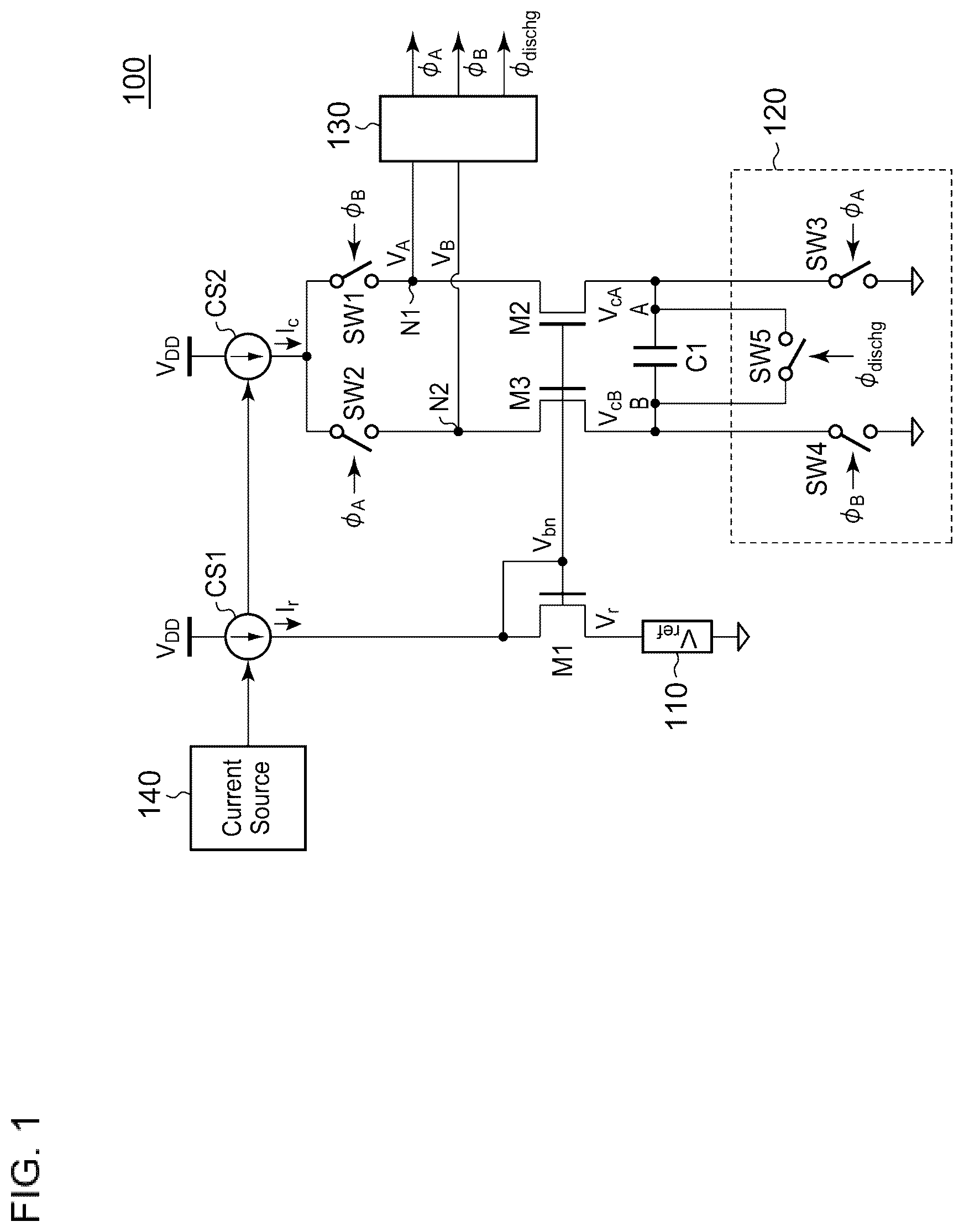
An oscillator circuit according to one embodiment includes: a first current source structured to generate a first current; a second current source structured to generate a second current; a first node and a second node; a first transistor having a drain coupled to the first current source; a reference voltage circuit structured to generate a reference voltage at a source of the first transistor; a capacitor; a second transistor having a source coupled to a first end of the capacitor, a drain coupled to the first node, and a gate coupled to a gate of the first transistor; a third transistor having a source coupled to a second end of the capacitor, a drain coupled to the second node, and a gate coupled to the gate of the first transistor; a first switch coupled between the first node and the second current source; a second switch coupled between the second node and the second current source; a charging/discharging circuit comprising a third switch coupled between the first end of the capacitor and a ground and a fourth switch coupled between the second end of the capacitor and the ground; and a control circuit structured to switch between (i) a first state in which the second switch and the third switch are turned on and the first switch and the fourth switch are turned off and (ii) a second state in which the second switch and the third switch are turned off and the first switch and the fourth switch are turned on based on a first voltage that occurs at the first node and a second voltage that occurs at the second node, and to control the charging/discharging circuit so as to discharge the capacitor in a discharging period that is a first portion of the first state and a discharging period that is a first portion of the second state. With this configuration, this requires a single capacitor to generate a pulse signal with a duty cycle of 50%. This allows the circuit area to be reduced as compared with an arrangement including two capacitors. In one embodiment, the charging/discharging circuit may further include a fifth switch coupled in parallel with the capacitor and structured to be turned on in the discharging period. In one embodiment, the control circuit may turn on the third switch and the fourth switch in the discharging period. In one embodiment, the charging/discharging circuit may further include: a sixth switch coupled between the first node and the ground; and a seventh switch coupled between the second node and the ground. Also, the control circuit may turn off the sixth switch and turn on the seventh switch in the first state. Also, the control circuit may turn on the sixth switch and turn off the seventh switch in the second state. In one embodiment, the oscillator circuit may further include a reference current source structured to generate a reference current. Also, the first current source may generate a first current that corresponds to the reference current. The second current source may generate a second current that corresponds to the reference current. In one embodiment, the reference current source may include a β-multiplier self-bias circuit. In one embodiment, the first transistor, the reference voltage circuit, and the first current source may be configured to also function as a part of the β-multiplier self-bias circuit. This allows the circuit area to be further reduced. Also, the reference voltage circuit also include a resistor. In one embodiment, the reference voltage circuit may include a reference voltage source. In one embodiment, the reference voltage circuit may include an NMOS transistor having a gate that receives a bias voltage. In one embodiment, the control circuit may include: a flipflop structured to be set according to the first voltage and to be reset according to the second voltage; and a pulse generator structured to generate a discharging control signal to be asserted in a predetermined period in response to a state transition of the flipflop. Embodiments Description will be made below regarding preferred embodiments with reference to the drawings. The same or similar components, members, and processes are denoted by the same reference numerals, and redundant description thereof will be omitted as appropriate. The embodiments have been described for exemplary purposes only and are by no means intended to restrict the present invention. Also, it is not necessarily essential for the present invention that all the features or a combination thereof be provided as described in the embodiments. In the present specification, a state represented by the phrase “the member Ais coupled to the member B” includes a state in which the member A is indirectly coupled to the member B via another member that does not substantially affect the electric connection between them, or that does not damage the functions or effects of the connection between them, in addition to a state in which they are physically and directly coupled. Similarly, a state represented by the phrase “the member C is provided between the member A and the member B” includes a state in which the member A is indirectly coupled to the member C, or the member B is indirectly coupled to the member C via another member that does not substantially affect the electric connection between them, or that does not damage the functions or effects of the connection between them, in addition to a state in which they are directly coupled. is a circuit diagram of an oscillator circuit 100 according to an embodiment. The oscillator circuit 100 includes a first current source CS 1 , a second current source CS 2 , a first transistor M 1 to a third transistor M 3 each configured as an NMOS transistor, a first node N 1 , a second node N 2 , a reference voltage circuit 110 , a charging/discharging circuit 120 , a reference current source 140 , a capacitor C 1 , a first switch SW 1 , and a second switch SW 2 , which are integrated on a single semiconductor substrate. A first current source CS 1 generates a first current Ir. The second current source CS 2 generates a second current Ic. The first current Ir and the second current Ic are each generated according to a reference current I ref generated by the reference current source 140 . The first transistor M 1 is arranged with its drain coupled to the first current source CS 1 . The reference voltage circuit 110 generates a reference voltage Vr at the source of the first transistor M 1 . The second transistor M 2 is arranged with its source coupled to a first end A of the capacitor C 1 , its drain coupled to a first node N 1 , and its gate coupled to a gate of the first transistor M 1 . The third transistor M 3 is arranged with its source coupled to a second end B of the capacitor C 1 , its drain coupled to the second node N 2 , and its gate coupled to the gate of the first transistor M 1 . A bias voltage Von generated at the gate of the first transistor M 1 is supplied to the gates of the second transistor M 2 and the third transistor M 3 . The first switch SW 1 is coupled between the first node N 1 and the second current source C 2 . The second switch SW 2 is coupled between the second node N 2 and the second current source CS 2 . The charging/discharging circuit 120 includes a third switch SW 3 coupled between the first end A of the capacitor C 1 and the ground and a fourth switch SW 4 coupled between the second end B of the capacitor C 1 and the ground. The charging/discharging circuit 120 further includes a fifth switch SW 5 coupled in parallel with the capacitor C 1 . The control circuit 130 controls the first switch SW 1 to the fifth switch SW 5 based on the first voltage V A generated at the first node N 1 and the second voltage V B generated at the second node N 2 . The control circuit 130 switches between (i) the first state ϕA in which the first switch SW 1 and the fourth switch SW 4 are turned off and the second switch SW 2 and the third switch SW 3 are turned on, and (ii) the second state ϕ B in which the first switch SW 1 and the fourth switch SW 4 are turned on and the second switch SW 2 and the third switch SW 3 are turned off. Furthermore, the control circuit 130 controls the charging/discharging circuit 120 so as to discharge the capacitor C 1 in a discharging period ϕ dischg , which is the first portion of the first state ϕ A , and a discharging period ϕ dischg , which is the first portion of the second state ϕ B . With the present embodiment, in the discharging period ϕ dischg , the fifth switch SW 5 is turned on so as to reset the charge stored in the capacitor C 1 . In , the reference symbols ϕ A , ϕ B , and ϕ dischg each represent a state. Furthermore, the reference symbols ϕA, ϕ B , and ϕ dischg each represent a control signal to be supplied to a switch to be turned on in the corresponding state. The above is the configuration of the oscillator circuit 100 . Next, description will be made regarding the operation thereof. is a circuit diagram of the oscillator circuit 100 in the first state A. In the first state ϕ A , the second switch SW 2 and the third switch SW 3 are turned on and the first switch SW 1 and the fourth switch SW 4 are turned off. In this state, the third switch SW 3 is turned on. Accordingly, the electric potential at the first end A of the capacitor C 1 decreases toward 0 V. Furthermore, the second switch SW 2 is turned on. Accordingly, the second current Ic generated by the second current source CS 2 is supplied to the second end B of the capacitor C 1 via the second switch SW 2 and the third transistor M 3 . During the discharging period ϕ dischg , which is the first portion of the first state ϕ A , the fifth switch SW 5 is turned on. Accordingly, the voltage V cB at the second end B of the capacitor C 1 becomes equal to the voltage V cA at the first end A. After the discharging period ϕ dischg ends, the fifth switch SW 5 is turned off. In this state, the capacitor C 1 is charged by the second current Ic. Accordingly, the voltage V cB at the second end B rises with time. This leads to an increase in the second voltage V B at the second node N 2 . The oscillator circuit 100 operates as a comparator that compares a reference voltage Vr with the voltage V cB at the second end B of the capacitor C 1 in the first state ϕ A . When the second voltage V B exceeds a given threshold value Vt, the control circuit 130 transits to the second state ϕ B . In the second state ϕ B , the oscillator circuit 100 provides an operation that is symmetrical to that in the first state ϕ A . That is to say, the first voltage V A rises with time. When the first voltage V A exceeds the threshold value Vt, the control circuit 130 transits to the first state ϕ A . is a waveform diagram showing the operation of the oscillator circuit 100 shown in . First State ϕ A At the time to, the oscillator circuit 100 becomes the first state ϕ A . In this state, the third switch SW 3 is turned on. Accordingly, the voltage V cA at the first end A of the capacitor C 1 decreases. Furthermore, the first portion of the first state ϕ A functions as the discharging period ϕ dischg . In this period, the fifth switch SW 5 is turned on. Accordingly, the voltage V cB at the second end B approaches the voltage V cA at the first end A. When the discharging period ϕ dischg ends and the fifth switch SW 5 is turned off at the time t 1 , the voltage V cB rises with a constant slope determined by the second current Ic. At the time t 2 after the time constant τ CR determined by the circuit constant elapses from the time t 1 , the voltage V cB exceeds the reference voltage Vr. In this state, the voltage V B increases together with the voltage V cB and exceeds a judgment threshold voltage Vt of the control circuit 130 . Accordingly, the control circuit 130 transits to the second state ϕ B at the time t 3 after a delay time τ COMP defined for comparison elapses. Second State ϕ B When the oscillator circuit 100 becomes the second state ϕ B at the time t 3 , the fourth switch SW 4 is turned on, leading to a decrease in the voltage V cB at the second end B of the capacitor C 1 . Furthermore, the first portion of the second state ϕ B functions as the discharging period ϕ dischg . In this period, the fifth switch SW 5 is turned on. Accordingly, the voltage V cA at the first end A approaches the voltage V cB at the second end B. When the discharging period ϕ dischg ends and the fifth switch SW 5 is turned off at the time t 4 , the voltage V cA rises with a constant slope determined by the second current Ic. The voltage V cA exceeds the reference voltage Vr at the time t 5 . In this state, the voltage V A rises together with the voltage V cA and exceeds a judgment threshold voltage Vt of the control circuit 130 . Accordingly, the control circuit 130 transits to the first state ϕ A at the time to after the delay time τ comp defined for comparison elapses. The above is the operation of the oscillator circuit 100 . The oscillation period T OSC of the oscillator circuit 100 is represented by the following Expression. T OSC = τ dischg + τ C R + τ c o m p Here, τ dischg represents the length of the discharging period ϕ dischg . The advantage of the oscillator circuit 100 can be clearly understood based on a comparison with an oscillator circuit 100 R according to a comparison technique. Description will be made regarding the comparison technique. is a circuit diagram of an oscillator circuit 100 R according to the comparison technique. The oscillator circuit 100 R includes two capacitors C 1 and C 2 . The first end of the first capacitor C 1 is grounded, and the second end thereof is coupled to the source of the second transistor M 2 . The third switch SW 3 is coupled in parallel with the first capacitor C 1 . The first end of the second capacitor C 2 is grounded, and the second end thereof is coupled to the source of the third transistor M 3 . The fourth switch SW 4 is coupled in parallel with the capacitor C 2 . In the comparison technique, the discharging period ϕ dischg is not provided. The control circuit 130 R alternately repeats the first state ϕ A and the second state ϕ B based on the first voltage V A at the first node N 1 and the second voltage V B at the second node N 2 . is a waveform diagram showing the operation of the oscillator circuit 100 R shown in . First State ϕ A In the second state ϕ B before the time to, the fourth switch SW 4 is turned on. Accordingly, the voltage V cB across the capacitor C 2 becomes 0 V. At the time to, the oscillator circuit 100 R becomes the first state ϕ A . In this state, the third switch SW 3 is turned on. Accordingly, the voltage V cA across the capacitor C 1 decreases. In the first state ϕ A , the voltage V cB across the second capacitor C 2 rises with a constant slope determined by the second current Ic. At the time t 2 , the voltage V cB exceeds the reference voltage Vr. In this state, the voltage V B rises together with the voltage V cB and exceeds the judgment threshold voltage Vt of the control circuit 130 . Accordingly, at the time t 3 after the delay time τ comp defined for comparison elapses, the control circuit 130 transits to the second state ϕ B . Second State ϕ B When the oscillator circuit 100 R becomes the second state ϕ B at the time t 3 , the voltage V cA across the first capacitor C 1 rises with a constant slope determined by the second current Ic. The voltage V cA exceeds the reference voltage Vr at the time t 5 . In this state, the voltage V A rises together with the voltage V cA and exceeds the judgment threshold voltage Vt of the control circuit 130 . Accordingly, the o control circuit 130 transits to the first state ϕ A at the time to after the delay time τ comp defined for comparison elapses. The above is the operation of the oscillator circuit 100 R. With the comparison technique employing the two capacitors C 1 and C 2 , this provides the following advantages. First Advantage This is capable of generating a pulse signal with a duty cycle of 50%. Second Advantage During a period in which one of the two capacitors C 1 and C 2 is being charged, the other capacitor (C 2 or C 1 ) is being discharged. With this, the period τdelay in which the capacitor C 2 (C 1 ) is being discharged has no effect on the oscillation period T OSC . Accordingly, the oscillation period T OSC is determined by the comparison time τ comp and the time constant τ CR . T OSC = τ comp + τ C R Third Advantage This allows the discharging time τ delay to be designed to be short. This allows the oscillation period T OSC to be easily shortened. In other words, this allows the oscillation frequency f OCS (=1/T OSC ) to be easily increased. However, the oscillator circuit 100 according to the comparison technique requires two capacitors C 1 and C 2 . The capacitors C 1 and C 2 each occupy a relatively large area on a semiconductor substrate. This leads to difficulty in designing the oscillator circuit 100 R to have a compact size. Returning to the embodiment, description will be made. The oscillator circuit 100 according to the embodiment provides the three advantages obtained with the comparison technique. In addition, the present embodiment allows the number of the capacitors to be reduced to one. This allows the circuit area to be reduced. The present disclosure encompasses various kinds of apparatuses and methods that can be regarded as a block configuration or a circuit configuration shown in , or otherwise that can be derived from the aforementioned description. That is to say, the present disclosure is not restricted to a specific configuration. More specific description will be made below regarding example configurations or examples for clarification and ease of understanding of the essence of the present disclosure and the present invention and the operation thereof. That is to say, the following description will by no means be intended to restrict the technical scope of the present disclosure. Example 1 is a circuit diagram of an oscillator circuit 100 A according to an example 1. The control circuit 130 includes a flipflop 132 and a pulse generator 134 . The flipflop 132 is configured as an SR latch (SR flipflop) and receives the first voltage V A at the first node N 1 via its set terminal(S) and the voltage V B at the second node N 2 via its reset terminal (R). The non-inverting output Q of the flipflop 132 is used as a control signal for an element configured to turn on in the first state ϕ A . The inverting output/Q of the flipflop 132 is used as a control signal for an element configured to turn on in the second state ϕ B . The pulse generator 134 generates a discharging control signal ϕ dischg based on at least one of the outputs Q and/Q (“/” represents logical inversion) of the flipflop 132 . During the discharging time τ dischg , the pulse generator 134 generates a pulse signal (discharging control signal ϕ dischg ) that becomes a predetermined level (e.g., high level) in response to the state transition of the flipflop 132 . The reference current source 140 includes a so-called β-multiplier self-bias circuit. Specifically, the reference current source 140 includes NMOS transistors M 11 and M 13 , PMOS transistors M 12 and M 14 , and a resistor R 11 . The first current source CS 1 includes a fourth transistor M 4 . The second current source CS 2 includes a fifth transistor M 5 . The fourth transistor M 4 and the fifth transistor M 5 form a current mirror circuit together with the transistor M 12 of the reference current source 140 . A first current Ir that is proportional to the reference current I ref generated by the reference current source 140 flows through the fourth transistor M 4 . A second current Ic that is proportional to the reference current I ref flows through the fifth transistor M 5 . Furthermore, in the present embodiment, the reference voltage circuit 110 includes a first resistor R 1 . Accordingly, the reference voltage Vr is represented by Ir×R 1 . is a circuit diagram showing an example configuration of the pulse generator 134 . The pulse generator 134 includes inverters INV 1 through INV 4 , AND gates AND 1 and AND 2 , and an OR gate OR 1 . The inverters INV 1 and INV 2 delay the output Q of the SR flipflop that is a previous stage. The delay time provided by the two inverters INV 1 and INV 2 corresponds to the discharging time τ dischg . The AND gate AND 1 generates the logical AND of the output Qd after the delay and the output Q before the delay. The output of the AND gate AND 1 is configured as a pulse signal that becomes the high level during the delay time τ dischg from a positive edge of the output Q. Similarly, the inverters INV 3 and INV 4 delay the inverting output/Q of the previous SR flip-flop. The AND gate AND 2 generates the logical AND of the inverting output/Q after the delay and the inverting output/Q before the delay. The output of the AND gate AND 2 is configured as a pulse signal that becomes the high level during the delay time τ dischg from a positive edge of the inverting output/Q. The OR gate OR 1 generates the logical OR of the outputs of the AND gates AND 1 and AND 2 , and outputs the logical OR as the discharging control signal ϕ dischg . Example 2 is a circuit diagram of an oscillator circuit 100 B according to an example 2. In this example, the first transistor M 1 , the fourth transistor M 4 (first current source CS 1 ), and the resistor R 1 (reference voltage circuit 110 ) are built into the reference current source 140 B. In other words, the transistor M 12 of the β-multiplier self-bias circuit also functions as the first current source CS 1 (transistor M 4 shown in ). The transistor M 11 also functions as the first transistor M 1 . The resistor R 11 also functions as the reference voltage circuit 110 . With the embodiment 2, this allows the circuit area and the current consumption to be further reduced as compared with the example 1. is a more specific circuit diagram of the oscillator circuit 100 B shown in . The third switch SW 3 and the fourth switch SW 4 are each configured as an NMOS transistor. The gate of the third switch SW 3 receives an input of a first control signal QA that is at the high level in the first state ϕ A . The gate of the fourth switch SW 4 receives an input of a second control signal ϕ B that is at the high level in the second state ϕ B . The fifth switch SW 5 is configured as an NMOS transistor. The gate of the fifth switch SW 5 receives an input of a control signal that is at the high level in the discharging period ϕ dischg . The first switch SW 1 and the second switch SW 2 are each configured as a PMOS transistor. The PMOS transistor turns on when a low-level signal is input to its gate. Accordingly, the gate of the first switch SW 1 receives an input of the first control signal QA that is at the low level in the second state QB. The gate of the second switch SW 2 receives an input of the second control signal ϕ B in the second state ϕ B . Example 3 is a circuit diagram of an oscillator circuit 100 C according to an example 3. The charging/discharging circuit 120 C of the oscillator circuit 100 C further includes a sixth switch SW 6 and a seventh switch SW 7 . The sixth switch SW 6 is coupled between the first node N 1 and the ground. The sixth switch SW 6 turns on in the first state ϕ A . The seventh switch SW 7 is coupled between the second node N 2 and the ground. The seventh switch SW 7 turns on in the second state ϕ B . is a more specific circuit diagram of the oscillator circuit 100 C shown in . The sixth switch SW 6 and the seventh switch SW 7 are each configured as an NMOS transistor. The gate of the sixth switch SW 6 receives an input of the first control signal QA that is at the high level in the first state ϕ A . The gate of the seventh switch SW 7 receives an input of the second control signal ϕ B that is at the high level in the second state ϕ B . The above is the configuration of the oscillator circuit 100 C. Before description of the operation of the oscillator circuit 100 C, description will be made with reference to regarding a problem involved in the configuration that does not include the sixth switch SW 6 and the seventh switch SW 7 ( etc.). In the waveform diagram shown in , the voltages V A and V B at the first node N 1 and the second node N 2 decrease to a voltage region that is somewhat higher than 0 V during the discharging period ϕ dischg . In this state, the second transistor M 2 and the third transistor M 3 each operate in the linear region. Accordingly, the second transistor M 2 and the third transistor M 3 are readily affected by PVT (process, voltage, and temperature) variations. As a result, with the oscillator circuit 100 , there is the potential for frequency drift to occur in the oscillator circuit 100 due to temperature variation or power supply voltage variation. is a waveform diagram showing the operation of the oscillator circuit 100 C shown in . In the example 3, the oscillator circuit 100 C further includes the sixth switch SW 6 and the seventh switch SW 7 as additional components. This lowers the voltages V A and V B at the first node N 1 and the second node N 2 to the vicinity of 0 V during the discharging period ϕ dischg . This allows the effects of frequency drift to be mitigated. Example 4 is a circuit diagram of an oscillator circuit 100 D according to an example 4. In the example 4, the reference current source 140 D includes the first current source CS 1 , the first transistor M 1 , and the reference voltage circuit 110 D as built-in components in the same manner as in the example 2 ( ). The reference voltage circuit 110 D includes an NMOS transistor M 15 provided between the source of the NMOS transistor M 11 and the ground and a bias circuit 112 configured to supply a bias voltage Von to the gate of the NMOS transistor M 15 . The bias circuit 112 includes a PMOS transistor M 17 and an NMOS transistor M 16 . The gate of the PMOS transistor M 17 is coupled to the gates of the PMOS transistors M 12 and M 13 . The NMOS transistor M 16 is coupled between the drain of the PMOS transistor M 17 and the ground. Description will be made regarding preferable operating points of the reference current source 140 D. The PMOS transistors M 5 , M 12 , M 14 , and M 15 and NMOS transistors M 2 , M 3 , M 11 , and M 13 are each operated in the weak inversion region (sub-threshold region Vgs<Vth). The NMOS transistor M 16 is operated in the strong inversion region (Vgs>Vth). The NMOS transistor M 15 is operated in the strong inversion region (Vgs>Vth) and the linear region (Vds<VGs−Vth). With such an arrangement in which the operating points are designed as described above, this is capable of suppressing each current to the order of nanoamperes. This allows each element size to be reduced, thereby allowing the circuit area to be reduced. With an arrangement employing the resistor R 11 as shown in , in order to provide each current on the order of nanoamperes, such an arrangement requires a very large resistance, leading to a large circuit area. In contrast, with the present example employing the NMOS transistor M 15 that operates in the strong inversion region and the linear region instead of the resistor R 11 , this allows the circuit area to be further reduced. In addition, with such an arrangement without resistors, this allows the number of mask layers to be reduced, thereby allowing the cost of the manufacturing process to be reduced. Furthermore, the resistance characteristics of a MOS transistor have a positive temperature coefficient in the linear region. In contrast, the threshold value Vth of an NMOS transistor has a negative temperature coefficient. Accordingly, by adjusting the size of the transistor M 15 , this allows the temperature dependence of the current that flows through the β-multiplier self-bias circuit to be adjusted. This allows the frequency drift due to the temperature characteristics of τ comp and τ delay to be adjusted. Example 5 is a circuit diagram of an oscillator circuit 100 E according to an example 5. In the example 5, a reference voltage source such as a bandgap reference (BGR) circuit or the like is employed as the reference voltage circuit 110 E. In many cases, integrated circuits (ICs) and large scale integration (LSI) are each provided with a reference voltage source such as a bandgap reference circuit. Accordingly, with such an arrangement using a reference voltage generated by the reference voltage source instead of the resistor R 11 , such an arrangement allows the circuit area to be reduced while suppressing temperature drift of the frequency. Example 6 is a circuit diagram of a pulse generator 134 F according to an example 6. In this example, two fifth switches SW 5 A and SW 5 B are coupled in parallel with the capacitor C 1 . The pulse generator 134 F includes inverters INV 1 to INV 4 , and NOR gates NOR 1 and NOR 2 . The output of the NOR gate NOR 1 is used as a discharging control signal ϕ dischgB for the fifth switch SW 5 B. The output of the NOR gate NOR 2 is used as a discharging control signal ϕ dischgA for the fifth switch SW 5 A. Furthermore, the output of the inverter INV 3 is used as a control signal to be asserted in the first state ϕ A . The output of the inverter INV 4 is used as a control signal to be asserted in the second state ϕ B . The pulse generator 134 F shown in is formed of a NOR gate alone configured as a basic logical operation element. Such an arrangement eliminates the need for composite gates (OR 1 , AND 1 , AND 2 ). This provides an advantage of reduced circuit area and improved delay time. Example 7 is a circuit diagram of an oscillator circuit 100 G according to an example 7. The charging/discharging circuit 120 G includes a third switch SW 3 , a fourth switch SW 4 , and OR gates OR 3 and OR 4 , and the fifth switch SW 5 is omitted. The OR gate OR 3 supplies the logical OR of the control signals ϕ A and ϕ dischg to the third switch SW 3 . The OR gate OR 4 supplies the logical OR of the control signals ϕ B and ϕ dischg to the fourth switch SW 4 . In the discharging period ϕ dischg , both the third switch SW 3 and the fourth switch SW 4 are turned on. This sets the voltages V cA and V cB at both ends of the capacitor C 1 to 0 V, thereby discharging the capacitor C 1 . Modification The configurations of the examples 1 through 7 described above can be combined as desired, and such combinations are also included in the scope of the present disclosure. Usage The usage of the oscillator circuit 100 is not restricted in particular. For example, the oscillator circuit 100 is suitably employed in a timer circuit. The present embodiments described using specific terms show only an aspect of the mechanisms and applications of the present disclosure. Rather, various modifications and various changes in the layout can be made without departing from the spirit and scope of the present disclosure defined in appended claims. Notes An aspect of the technique disclosed in the present specification can be understood as follows. Item 1 An oscillator circuit comprising: a first current source structured to generate a first current, a second current source structured to generate a second current, a first node and a second node, a first transistor having a drain coupled to the first current source, a reference voltage circuit structured to generate a reference voltage at a source of the first transistor, a capacitor, a second transistor having a source coupled to a first end of the capacitor, a drain coupled to the first node, and a gate coupled to a gate of the first transistor, a third transistor having a source coupled to a second end of the capacitor, a drain coupled to the second node, and a gate coupled to the gate of the first transistor, a first switch coupled between the first node and the second current source, a second switch coupled between the second node and the second current source, a charging/discharging circuit comprising a third switch coupled between the first end of the capacitor and a ground and a fourth switch coupled between the second end of the capacitor and the ground; and a control circuit structured to switch between (i) a first state in which the second switch and the third switch are turned on and the first switch and the fourth switch are turned off and (ii) a second state in which the second switch and the third switch are turned off and the first switch and the fourth switch are turned on based on a first voltage that occurs at the drain of the second transistor and a second voltage that occurs at the drain of the third transistor, and to control the charging/discharging circuit so as to discharge the capacitor in a discharging period that is a first portion of the first state and a discharging period that is a first portion of the second state. Item 2 The oscillator circuit according to item 1, wherein the charging/discharging circuit further includes a fifth switch coupled in parallel with the capacitor and structured to be turned on in the discharging period. Item 3 The oscillator circuit according to item 1, wherein the control circuit turns on the third switch and the fourth switch in the discharging period. Item 4 The oscillator circuit according to any one of items 1 through 3, wherein the charging/discharging circuit further comprises: a sixth switch coupled between the first node and the ground; and a seventh switch coupled between the second node and the ground, wherein the control circuit turns on the sixth switch and turns off the seventh switch in the first state, and wherein the control circuit turns off the sixth switch and turns on the seventh switch in the second state. Item 5 The oscillator circuit according to any one of items 1 through 4, further comprising a reference current source structured to generate a reference current, wherein the first current source generates a first current that corresponds to the reference current, and wherein the second current source generates a second current that corresponds to the reference current. Item 6 The oscillator circuit according to item 5, wherein the reference current source comprises a β-multiplier self-bias circuit. Item 7 The oscillator circuit according to item 6, wherein the first transistor, the reference voltage circuit, and the first current source are structured to also function as a part of the β-multiplier self-bias circuit. Item 8 The oscillator circuit according to any one of items 1 through 7, wherein the reference voltage circuit comprises a resistor. Item 9 The oscillator circuit according to any one of items 1 through 7, wherein the reference voltage circuit comprises a reference voltage source. Item 10 The oscillator circuit according to any one of items 1 through 7, wherein the reference voltage circuit comprises an NMOS transistor with a gate thereof that receives a bias voltage. Item 11 The oscillator circuit according to any one of items 1 through 10, wherein the control circuit comprises: a flipflop structured to be set according to the first voltage and to be reset according to the second voltage; and a pulse generator structured to generate a discharging control signal to be asserted in a predetermined period in response to a state transition of the flipflop.
Figures (16)
Citations
This patent cites (2)
- US4395173
- US2020167527