Input Sensor and Display Device Including the Same
Abstract
A display device includes a display panel. An input sensor is disposed on the display panel. A first pattern of the input sensor includes mesh lines. A second pattern of the input sensor overlaps the first pattern with an insulating layer interposed therebetween, and includes mesh lines. The mesh lines of the first pattern include a first mesh line extending in the first reference direction, and the mesh lines of the second pattern include a second mesh line extending in the first reference direction and overlapping the first mesh line in a plan view. In a plan view, first cutting areas in which the first mesh line is partially cut and second cutting areas in which the second mesh line is partially cut do not overlap.
Claims (17)
1 . A display device comprising: a display panel including a display area where an image is displayed; and an input sensor disposed on the display panel, wherein the input sensor comprises: a first pattern including mesh lines in the display area; and a second pattern overlapping the first pattern with an insulating layer interposed therebetween and including mesh lines, wherein the mesh lines of the first pattern include a first mesh line extending in a first reference direction, the mesh lines of the second pattern include a second mesh line extending in the first reference direction and overlapping the first mesh line in a plan view, wherein, in a plan view, first cutting areas in which the first mesh line is partially cut and second cutting areas in which the second mesh line is partially cut do not overlap each other, wherein the input sensor further comprises: a first sensor electrode; and a second sensor electrode insulated from the first sensor electrode and crossing the first sensor electrode, wherein the first sensor electrode includes the first pattern and the second pattern, wherein the second pattern is connected to the first pattern through a contact hole formed through the insulating layer, wherein the second sensor electrode comprises: a third pattern including mesh lines, disposed in the same layer as the first pattern, and spaced apart from the first pattern; and a fourth pattern disposed in the same layer as the second pattern, spaced apart from the second pattern, overlapping the third pattern, connected to the third pattern through a contact hole formed through the insulating layer, and including mesh lines, wherein the first pattern includes first sensor areas and a first bridge area connecting the first sensor areas, wherein the second pattern includes second sensor areas overlapping the first sensor areas, wherein the third pattern includes third sensor areas and a dummy area spaced apart from the third sensor areas, wherein the fourth pattern includes fourth sensor areas overlapping the third sensor areas, and the first bridge area and a second bridge area connecting the fourth sensor areas and overlapping the dummy area, wherein a direction in which the first sensor areas are arranged and a direction in which the second sensor areas are arranged are the same, wherein a direction in which the third sensor areas are arranged and a direction in which the fourth sensor areas are arranged are the same, and wherein a direction in which the first sensor areas are arranged and a direction in which the third sensor areas are arranged cross each other.
14 . An input sensor comprising: a first pattern including mesh lines and disposed in a sensor area; and a second pattern overlapping the first pattern with an insulating layer interposed therebetween and including mesh lines, wherein the mesh lines of the first pattern include a first mesh line extending in a first reference direction, and the mesh lines of the second pattern include a second mesh line extending in the first reference direction and overlapping the first mesh line, wherein, in a plan view, first cutting areas in which the first mesh line is partially cut and second cutting areas in which the second mesh line is partially cut do not overlap each other, wherein the input sensor further comprises: a first sensor electrode; and a second sensor electrode insulated from the first sensor electrode and crossing the first sensor electrode, wherein the first sensor electrode includes the first pattern and the second pattern, wherein the second pattern is connected to the first pattern through a contact hole formed through the insulating layer, wherein the second sensor electrode comprises: a third pattern including mesh lines, disposed in the same layer as the first pattern, and spaced apart from the first pattern; and a fourth pattern disposed in the same layer as the second pattern, spaced apart from the second pattern, overlapping the third pattern, connected to the third pattern through a contact hole formed through the insulating layer, and including mesh lines, wherein the first pattern includes first sensor areas and a first bridge area connecting the first sensor areas, wherein the second pattern includes second sensor areas overlapping the first sensor areas, wherein the third pattern includes third sensor areas and a dummy area spaced apart from the third sensor areas, wherein the fourth pattern includes fourth sensor areas overlapping the third sensor areas, and the first bridge area and a second bridge area connecting the fourth sensor areas and overlapping the dummy area, wherein a direction in which the first sensor areas are arranged and a direction in which the second sensor areas are arranged are the same, wherein a direction in which the third sensor areas are arranged and a direction in which the fourth sensor areas are arranged are the same, and wherein a direction in which the first sensor areas are arranged and a direction in which the third sensor areas are arranged cross each other.
17 . An electronic device comprising: a display panel including a display area where an image is displayed; and an input sensor disposed on the display panel, wherein the input sensor comprises: a first pattern including mesh lines in the display area; and a second pattern overlapping the first pattern with an insulating layer interposed therebetween and including mesh lines, wherein the mesh lines of the first pattern include a first mesh line extending in a first reference direction, the mesh lines of the second pattern include a second mesh line extending in the first reference direction and overlapping the first mesh line in a plan view, wherein, in a plan view, first cutting areas in which the first mesh line is partially cut and second cutting areas in which the second mesh line is partially cut do not overlap each other, wherein the input sensor further comprises: a first sensor electrode; and a second sensor electrode insulated from the first sensor electrode and crossing the first sensor electrode, wherein the first sensor electrode includes the first pattern and the second pattern, wherein the second pattern is connected to the first pattern through a contact hole formed through the insulating layer, wherein the second sensor electrode comprises: a third pattern including mesh lines, disposed in the same layer as the first pattern, and spaced apart from the first pattern; and a fourth pattern disposed in the same layer as the second pattern, spaced apart from the second pattern, overlapping the third pattern, connected to the third pattern through a contact hole formed through the insulating layer, and including mesh lines, wherein the first pattern includes first sensor areas and a first bridge area connecting the first sensor areas, wherein the second pattern includes second sensor areas overlapping the first sensor areas, wherein the third pattern includes third sensor areas and a dummy area spaced apart from the third sensor areas, wherein the fourth pattern includes fourth sensor areas overlapping the third sensor areas, and the first bridge area and a second bridge area connecting the fourth sensor areas and overlapping the dummy area, wherein a direction in which the first sensor areas are arranged and a direction in which the second sensor areas are arranged are the same, wherein a direction in which the third sensor areas are arranged and a direction in which the fourth sensor areas are arranged are the same, and wherein a direction in which the first sensor areas are arranged and a direction in which the third sensor areas are arranged cross each other.
Show 14 dependent claims
2 . The display device according to claim 1 , wherein, in a plan view, the centers of the first cutting areas of the first mesh line are spaced apart from the centers of the second cutting areas of the second mesh line by a distance greater than a width of the first and second cutting areas.
3 . The display device according to claim 2 , wherein, in a plan view, the centers of the first cutting areas of the first mesh line are spaced apart from the centers of the second cutting areas of the second mesh line by a distance of about 2 μm or more.
4 . The display device according to claim 1 , wherein, in a plan view, the first cutting areas of the first mesh line are positioned along first cutting lines, the second cutting areas of the second mesh line are positioned along second cutting lines, and the first cutting lines and the second cutting lines extending along a same direction do not overlap each other.
5 . The display device according to claim 1 , wherein a line width of the first mesh line and a line width of the second mesh line are substantially the same.
6 . The display device according to claim 1 , wherein a line width of the second mesh line is greater than a line width of the first mesh line, and wherein, in a plan view, the second mesh line substantially covers the first mesh line.
7 . The display device according to claim 1 , wherein, in a plan view, at least a portion of the first cutting areas and the second cutting areas are positioned at an edge of the first sensor electrode.
8 . The display device according to claim 1 , wherein, in a plan view, the first cutting areas and the second cutting areas are positioned inside the first sensor electrode and spaced apart from a boundary between the first sensor electrode and the second sensor electrode.
9 . The display device according to claim 1 , wherein the input sensor is directly disposed on the display panel.
10 . The display device according to claim 1 , wherein the input sensor further comprises: a sensor electrode including the second pattern; and a sensing line including the first pattern and electrically connected to the sensor electrode.
11 . The display device according to claim 10 , wherein the input sensor further comprises a dummy line disposed in the same layer as the sensing line and including a mesh line overlapping the sensor electrode in a plan view, and wherein, in a plan view, third cutting areas in which the mesh line of the dummy line is partially cut do not overlap the second cutting areas.
12 . The display device according to claim 1 , wherein the input sensor further comprises: a sensor electrode including the second pattern; a dummy electrode including the first pattern; and a sensing line disposed in the same layer as the dummy electrode, including mesh lines overlapping the sensor electrode in a plan view, and electrically connected to the sensor electrode.
13 . The display device according to claim 12 , wherein the mesh lines of the sensing line do not include a cutting area therein.
15 . The input sensor according to claim 14 , wherein a line width of the second mesh line is greater than a line width of the first mesh line, and wherein, in a plan view, the second mesh line substantially covers the first mesh line.
16 . The input sensor according to claim 14 , further comprising: a sensor electrode including the second pattern; and a sensing line including the first pattern and electrically connected to the sensor electrode.
Full Description
Show full text →
This application claims priority to Korean Patent Application No. 10-2023-0100082, filed on Jul. 31, 2023, and all the benefits accruing therefrom under 35 U.S.C. § 119, the content of which in its entirety is herein incorporated by reference.
BACKGROUND
1. Field The disclosure relates to an input sensor and a display device. 2. Description of the Related Art A display device may include a display panel displaying an image and an input sensor sensing an external input. The input sensor may be integrally formed with the display panel through a successive process. Alternatively, the input sensor may be formed through a process separated from the display panel and then coupled to the display panel.
SUMMARY
An object of the disclosure is to provide an input sensor and a display device in which a sensor pattern is not visually recognized. According to embodiments of the disclosure, a display device includes a display panel including a display area where an image is displayed, and an input sensor disposed on the display panel. The input sensor includes a first pattern including mesh lines in the display area, and a second pattern overlapping the first pattern with an insulating layer interposed therebetween and including mesh lines. The mesh lines of the first pattern include a first mesh line extending in a first reference direction, and the mesh lines of the second pattern include a second mesh line extending in the first reference direction and overlapping the first mesh line in a plan view. In a plan view, first cutting areas in which the first mesh line is partially cut and second cutting areas in which the second mesh line is partially cut do not overlap each other. In a plan view, the first cutting areas of the first mesh line may be spaced apart from the second cutting areas of the second mesh line by a distance greater than a width of the first and second cutting areas. In a plan view, the first cutting areas of the first mesh line may be spaced apart from the second cutting areas of the second mesh line by a distance of about 2 μm or more. In a plan view, the first cutting areas of the first mesh line may be positioned along first cutting lines, the second cutting areas of the second mesh line may be positioned along second cutting lines, and the first cutting lines and the second cutting lines extending along a same direction may not overlap each other. A line width of the first mesh line and a line width of the second mesh line may be substantially the same. A line width of the second mesh line may be greater than a line width of the first mesh line, and in a plan view, the second mesh line may substantially cover the first mesh line. The input sensor may further include a first sensor electrode, and a second sensor electrode insulated from the first sensor electrode and crossing the first sensor electrode, the first sensor electrode may include the first pattern and the second pattern, and the second pattern may be connected to the first pattern through a contact hole formed through the insulating layer. In a plan view, at least a portion of the first cutting areas and the second cutting areas may be positioned at an edge of the first sensor electrode. In a plan view, the first cutting areas and the second cutting areas may be positioned inside the first sensor electrode and spaced apart from a boundary between the first sensor electrode and the second sensor electrode. The second sensor electrode may include a third pattern including mesh lines, disposed in the same layer as the first pattern, and spaced apart from the first pattern, and a fourth pattern disposed in the same layer as the second pattern, spaced apart from the second pattern, overlapping the third pattern, connected to the third pattern through a contact hole formed through the insulating layer, and including mesh lines. The first pattern may include first sensor areas and a first bridge area connecting the first sensor areas, the second pattern may include second sensor areas overlapping the first sensor areas, the third pattern may include third sensor areas and a dummy area spaced apart from the third sensor areas, the fourth pattern may include fourth sensor areas overlapping the third sensor areas and the first bridge area and a second bridge area connecting the fourth sensor areas and overlapping the dummy area, a direction in which the first sensor areas are arranged and a direction in which the second sensor areas are arranged may be the same, a direction in which the third sensor areas are arranged and a direction in which the fourth sensor areas are arranged may be the same, and a direction in which the first sensor areas are arranged and a direction in which the third sensor areas are arranged may cross each other. The input sensor may be directly disposed on the display panel. The input sensor may further include a sensor electrode including the second pattern, and a sensing line including the first pattern and electrically connected to the sensor electrode. The input sensor may further include a dummy line disposed in the same layer as the sensing line and including a mesh line overlapping the sensor electrode in a plan view, and in a plan view, third cutting areas in which the mesh line of the dummy line is partially cut may not overlap the second cutting areas. The input sensor may further include a sensor electrode including the second pattern, a dummy electrode including the first pattern, and a sensing line disposed in the same layer as the dummy electrode, including mesh lines overlapping the sensor electrode in a plan view, and electrically connected to the sensor electrode. The mesh lines of the sensing line may not include a cutting area therein. According to embodiments of the disclosure, an input sensor includes a first pattern including mesh lines and disposed in a sensor area, and a second pattern overlapping the first pattern with an insulating layer interposed therebetween and including mesh lines. The mesh lines of the first pattern include a first mesh line extending in a first reference direction, and the mesh lines of the second pattern include a second mesh line extending in the first reference direction and overlapping the first mesh line. In a plan view, first cutting areas in which the first mesh line is partially cut and second cutting areas in which the second mesh line is partially cut do not overlap each other. A line width of the second mesh line may be greater than a line width of the first mesh line, and in a plan view, the second mesh line may substantially cover the first mesh line. The input sensor may further include a first sensor electrode, and a second sensor electrode insulated from the first sensor electrode and crossing the first sensor electrode, the first sensor electrode may include the first pattern and the second pattern, and the second pattern may be connected to the first pattern through a contact hole formed through the insulating layer. The input sensor may further include a sensor electrode including the second pattern, and a sensing line including the first pattern and electrically connected to the sensor electrode. In the input sensor and the display device according to embodiments of the disclosure, a sensor pattern may have a two-layer structure including the first pattern and the second pattern that substantially overlap each other, and the first cutting area of the mesh line of the first pattern and the second cutting area of the mesh line of the second pattern may not overlap each other. Therefore, a difference between a light amount in each of the first and second cutting areas and a light amount in remaining areas (that is, a light reflected by the mesh line) may be minimized, and the sensor pattern may not be visually recognized. In addition, the line width of the mesh line of the second pattern may be greater than the line width of the mesh line of the first pattern, and the second pattern may cover the first pattern in a plan view. Therefore, light may be reflected by the second pattern in an area other than the second cutting area, light may be reflected by the first pattern in the second cutting area, a light amount (that is, a light amount reflected by the mesh line) becomes identical or similar throughout the input sensor and display device, and the sensor pattern may not be visually recognized. Furthermore, the sensing line disposed in the sensor area and overlapping the sensor pattern may include the dummy cutting area corresponding to the second cutting area of the mesh line of the sensor pattern, and the dummy cutting area may not overlap the second cutting area. Therefore, the sensing line may also not be visually recognized. An effect according to embodiments is not limited by the content exemplified above, and more various effects are included in the present specification.
BRIEF DESCRIPTION OF THE DRAWINGS
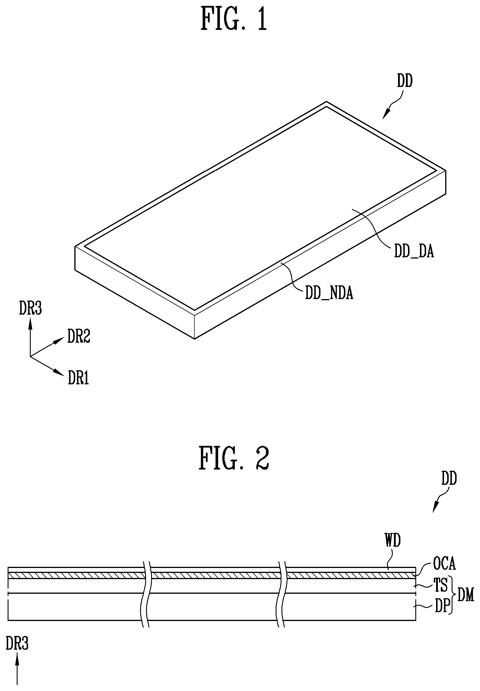
The above and other features of the disclosure will become more apparent by describing in further detail embodiments thereof with reference to the accompanying drawings, in which: is a perspective view schematically illustrating a display device according to embodiments of the disclosure; is a schematic cross-sectional view of the display device of ; is a schematic cross-sectional view of a display panel in the display device of ; is a schematic cross-sectional view of a touch sensor in the display device of ; is a plan view schematically illustrating an embodiment of the touch sensor of ; are enlarged plan views of an AA area of ; is a cross-sectional view taken along a line I-I′ of ; is a cross-sectional view taken along a line II-II′ of ; is a diagram illustrating an optical characteristic of the touch sensor; is a diagram illustrating an image obtained by capturing the touch sensor; is an enlarged plan view of a BB area of ; is a cross-sectional view taken along a line III-III′ of ; , 15 , and 16 are enlarged plan views of the BB area of ; is a plan view schematically illustrating an embodiment of the touch sensor of ; is an enlarged plan view of a CC area of ; are enlarged plan views of a DD area of ; is an enlarged plan view of the CC area of ; is an enlarged plan view of an EE area of ; is an enlarged plan view of the CC area of ; is an enlarged plan view of an FF area of ; is an enlarged plan view of the CC area of ; and is an enlarged plan view of a GG area of .
DETAILED
DESCRIPTION OF THE EMBODIMENT
The disclosure may be modified in various manners and have various forms. Therefore, specific embodiments will be illustrated in the drawings and will be described in detail in the specification. However, it should be understood that the disclosure is not intended to be limited to the disclosed specific forms, and the disclosure includes all modifications, equivalents, and substitutions within the spirit and technical scope of the disclosure. Terms of “first”, “second”, and the like may be used to describe various components, but the components should not be limited by the terms. The terms are used only for the purpose of distinguishing one component from another component. For example, without departing from the scope of the disclosure, a first component may be referred to as a second component, and similarly, a second component may also be referred to as a first component. In the following description, the singular expressions include plural expressions unless the context clearly dictates otherwise. It should be understood that in the present application, a term of “include”, “have”, or the like is used to specify that there is a feature, a number, a step, an operation, a component, a part, or a combination thereof described in the specification, but does not exclude a possibility of the presence or addition of one or more other features, numbers, steps, operations, components, parts, or combinations thereof in advance. In addition, a case where a portion of a layer, a layer, an area, a plate, or the like is referred to as being “on” another portion, it includes not only a case where the portion is “directly on” another portion, but also a case where there is further another portion between the portion and another portion. In addition, in the present specification, when a portion of a layer, a layer, an area, a plate, or the like is formed on another portion, a forming direction is not limited to an upper direction but includes forming the portion on a side surface or in a lower direction. On the contrary, when a portion of a layer, a layer, an area, a plate, or the like is formed “under” another portion, this includes not only a case where the portion is “directly beneath” another portion but also a case where there is further another portion between the portion and another portion. In the following description, a case where a portion is connected to another portion includes a case where they are electrically connected to each other with another element interposed therebetween as well as a case in which they are directly connected to each other. In an embodiment of the disclosure, a term “connection” between two configurations may mean that both of an electrical connection and a physical connection are inclusively used. Hereinafter, a display device according to embodiments is described with reference to drawings. is a perspective view schematically illustrating a display device according to embodiments of the disclosure. is a schematic cross-sectional view of the display device of . is a schematic cross-sectional view of a display panel in the display device of . is a schematic cross-sectional view of a touch sensor in the display device of . Referring to to 4 , when the display device DD is an electronic device which includes a display surface such as a smartphone, a television, a tablet PC, a mobile phone, a video phone, an e-book reader, a desktop PC, a laptop PC, a netbook computer, a workstation, a server, a PDA, a portable multimedia player (PMP), an MP3 player, a medical device, a camera, or a wearable, the disclosure may be applied to the display device DD. The display device DD may have various shapes, and for example, the display device DD may have a rectangular plate shape having two pairs of sides parallel to each other, but the disclosure is not limited thereto. When the display device DD has the rectangular plate shape, one pair of sides of the two pairs of sides may be longer than the other pair of sides. In the drawing, the display device DD has an angled corner portion formed of a straight line, but the disclosure is not limited thereto. According to an embodiment, the display device DD having the rectangular plate shape may have a round corner portion where one long side and one short side contact each other. In an embodiment of the disclosure, for convenience of description, the display device DD has the rectangular shape having a pair of long sides and a pair of short sides, and an extension direction of the long side is indicated as a second direction DR 2 , an extension direction of the short side is indicated as a first direction DR 1 , and a direction perpendicular to the extension directions of the long side and the short side is indicated as a third direction DR 3 . The first to third directions DR 1 , DR 2 , and DR 3 may refer to directions indicated by the first to third directions DR 1 , DR 2 , and DR 3 , respectively. In an embodiment of the disclosure, at least a portion of the display device DD may have flexibility, and the display device DD may be folded at a portion having flexibility. The display device DD may include a display area DD_DA displaying an image and a non-display area DD_NDA provided on at least one side of the display area DD_DA. The non-display area DD_NDA is an area in which an image is not displayed. However, the disclosure is not limited thereto. According to an embodiment, a shape of the display area DD_DA and a shape of the non-display area DD_NDA may be relatively designed. According to an embodiment, the display device DD may include a sensing area and a non-sensing area. The display device DD may not only display an image through the sensing area, but also sense a touch input performed on a display surface or sense light incident from a front direction. The non-sensing area may surround the sensing area, but this is an example and may not be limited thereto. According to an embodiment, a partial area of the display area DA may correspond to the sensing area. The display device DD may include a display module DM and a window WD. The display module DM may include a display panel DP and a touch sensor TS. The display panel DP may display an image through the display area DD_DA. As the display panel DP, a display panel capable of self-emission, such as an organic light emitting display panel (OLED panel) using an organic light emitting diode as a light emitting element, an ultra-small light emitting diode display panel (nano-scale LED display panel) using an ultra-small light emitting diode as a light emitting element, and a quantum dot organic light emitting display panel (QD OLED panel) using a quantum dot and an organic light emitting diode may be used. In addition, as the display panel DP, a non-emission display panel such as a liquid crystal display panel (LCD panel), an electro-phoretic display panel (EPD panel), and an electro-wetting display panel (EWD panel) may be used. When the non-emission display panel is used as the display panel DP, the display device DD may include a backlight unit that supplies light to the display panel DP. The display panel DP may include a substrate SUB, a pixel circuit layer PCL, a display element layer DPL, and a thin film encapsulation layer TFE. The substrate SUB may be a rigid substrate or a flexible substrate. Here, when the substrate SUB is the rigid substrate, the substrate SUB may be one of a glass substrate, a quartz substrate, a glass ceramic substrate, and a crystalline glass substrate. When the substrate SUB is the flexible substrate, the substrate SUB may be one of a film substrate and a plastic substrate including a polymer organic material. In addition, the substrate SUB may include fiber glass reinforced plastic (FRP). The pixel circuit layer PCL may be disposed on the substrate SUB. In the pixel circuit layer PCL, a plurality of thin film transistors and signal lines connected to the thin film transistors may be disposed. For example, each thin film transistor may have a shape in which a semiconductor layer, a gate electrode, and a source/drain electrode are sequentially stacked with an insulating layer interposed therebetween. The semiconductor layer may include amorphous silicon, poly silicon, low temperature poly silicon, and an organic semiconductor. The gate electrode and the source/drain electrode may include one of aluminum (Al), copper (Cu), titanium (Ti), and molybdenum (Mo), but the disclosure is not limited thereto. In addition, the pixel circuit layer PCL may include one or more insulating layers. The display element layer DPL may be disposed on the pixel circuit layer PCL. The display element layer DPL may include a light emitting element emitting light. The light emitting element may be, for example, an organic light emitting diode, but the disclosure is not limited thereto. According to an embodiment, the light emitting element may be an inorganic light emitting element including an inorganic light emitting material or a light emitting element (a quantum dot display element) that emits light by changing a wavelength of light emitted using a quantum dot. The organic light emitting diode may have, for example, a shape in which an anode electrode, a hole transport layer, an organic light emitting layer, an electron transport layer, and a cathode electrode are sequentially stacked, but is not limited thereto. The thin film encapsulation layer TFE may be disposed on the display element layer DPL. The thin film encapsulation layer TFE may be an encapsulation substrate or may have a shape of an encapsulation layer formed of multiple layers. When the thin film encapsulation layer TFE has the shape of the encapsulation layer, the thin film encapsulation layer TFE may include an inorganic layer and/or an organic layer. For example, the thin film encapsulation layer TFE may have a shape in which an inorganic layer, an organic layer, and an inorganic layer are sequentially stacked. The thin film encapsulation layer TFE may prevent external air and moisture from penetrating into the display element layer DPL and the pixel circuit layer PCL. The touch sensor TS (an input sensor, or an input sensing device) may be directly formed on a surface on which an image of the display panel DP is emitted to receive a user's touch input and/or a hover input. Here, “directly formed” may mean that the touch sensor is formed by a successive process and is attached to the surface on which the image of the display panel DP is emitted without a separate adhesive layer. The touch sensor TS may sense a touch capacitance when input means such as a user's hand or a conductor contact and/or approach close to the touch sensor to recognize the touch input and/or the hover input of the display device DD. Here, the touch input may mean a direct touch (or contact) by the user's hand or the separate input means, and the hover input may mean that the user's hand or the separate input means is near the display device DD including the touch sensor TS but does not touch the display device DD. The touch sensor TS may have a multiple layer structure. The touch sensor TS may include at least one or more conductive layers and may include at least one or more insulating layers. The touch sensor TS may include a base layer BSL, a first conductive layer CPL 1 , a first insulating layer TS_INS 1 , a second conductive layer CPL 2 , and a second insulating layer TS_INS 2 . The first conductive layer CPL 1 may be directly disposed on the thin film encapsulation layer TFE of the display panel DP, but the disclosure is not limited thereto. According to an embodiment, another insulating layer, for example, the base layer BSL, may be disposed between the first conductive layer CPL 1 and the thin film encapsulation layer TFE. In this case, the first conductive layer CPL 1 may be directly disposed on the base layer BSL. Each of the first and second conductive patterns CP 1 and CP 2 may have a single layer structure or may have a multiple layer structure stacked in a thickness direction, for example, the third direction DR 3 . The conductive layer of the single layer structure may include a conductive material. For example, the conductive material may include a metal such as molybdenum (Mo), silver (Ag), titanium (Ti), copper (Cu), aluminum (Al), and an alloy thereof, or may include transparent conductive oxide such as indium tin oxide (ITO), indium zinc oxide (IZO), zinc oxide (ZnO), or indium tin zinc oxide (ITZO). The conductive layer of the multiple layer structure may include metal layers of multiple layers. The metal layers of multiple layers may have, for example, a triple structure of titanium (Ti)/aluminum (Al)/titanium (Ti), but are not limited thereto. The conductive layer of the multiple layer structure may include metal layers of multiple layers and a transparent conductive layer. In an embodiment of the disclosure, each of the first and second conductive layers CPL 1 and CPL 2 may include sensor patterns SP (refer to ) and sensing lines SL (refer to ). Each of the first and second insulating layers TS_INS 1 and TS_INS 2 may include an inorganic material or an organic material. The inorganic material may include at least one of an inorganic insulating layer such as silicon nitride (SiN x ), silicon oxide (SiO x ), silicon oxynitride (SiON), and aluminum oxide (AlO x ). The organic material may include at least one of acryl-based resin, methacryl-based resin, polyisoprene, vinyl-based resin, epoxy-based resin, urethane-based resin, cellulose-based resin, siloxane-based resin, polyimide-based resin, polyamide-based resin, and perylene-based resin. The window WD for protecting an exposed surface of a display module DM may be provided on the display module DM. The window WD may protect the display module DM from external impact and provide an input surface and/or a display surface to the user. The window WD may be coupled to the display module DM using an optically transparent adhesive OCA. The window WD may have a multilayer structure selected from a glass substrate, a plastic film, and a plastic substrate. Such a multilayer structure may be formed through a successive process or an adhesion process using an adhesive layer. The entire or a portion of the window WD may have flexibility. is a plan view schematically illustrating an embodiment of the touch sensor of . are enlarged plan views of an AA area of . is a cross-sectional view taken along a line I-I′ of . is a cross-sectional view taken along a line II-II′ of . is a diagram illustrating an optical characteristic of the touch sensor. is a diagram illustrating an image obtained by capturing the touch sensor. Referring to , 4 , and 5 , the touch sensor TS (or the base layer BSL) may include a sensor area SA (a sensing area, or an active area) capable of sensing a touch input and a non-sensor area NSA (or a non-sensing area) surrounding at least a portion of the sensor area SA and not capable of sensing the touch input. The base layer BSL may be formed of tempered glass, transparent plastic, or a transparent film. According to an embodiment, the base layer BSL may be omitted. The sensor area SA may be provided in a central portion of the base layer BSL to overlap the display area DD_DA (refer to ). The sensor area SA may be provided in substantially the same shape as a shape of the display area DD_DA, but is not limited thereto. A sensor electrode for sensing the touch input may be provided and/or formed in the sensor area SA. The non-sensor area NSA may be provided in a peripheral area of the base layer BSL to overlap the non-display area DD_NDA (refer to ). Here, the peripheral area may be an area surrounding the central portion of the base layer BSL. A sensing line SL electrically connected to the sensor electrode to receive and transfer a sensing signal is provided and/or formed in the non-sensing area DD_NSA. In addition, a pad unit PDA connected to the sensing line SL and electrically connected to the sensor electrode of the sensor area SA may be disposed in the non-sensor area NSA. The pad unit PDA may include a pad PD. The sensing line SL may include a plurality of first sensing lines SL 1 and a plurality of second sensing lines SL 2 . The sensor electrode may include a plurality of sensor patterns SP and first and second bridge patterns BRP 1 and BRP 2 . The sensor patterns SP may include a plurality of first sensor patterns SP 1 (or first sensor electrodes) and a plurality of second sensor patterns SP 2 (or second sensor electrodes) electrically insulated from the first sensor patterns SP 1 . The first sensor patterns SP 1 may be arranged in the first direction DR 1 and may be electrically connected to the adjacent first sensor patterns SP 1 by the first bridge patterns BRP 1 to configure at least one sensor row. The second sensor patterns SP 2 may be arranged in the second direction DR 2 crossing the first direction DR 1 and may be electrically connected to the adjacent second sensor patterns SP 2 through the second bridge patterns BRP 2 to configure at least one sensor column. Each of the first and second sensor patterns SP 1 and SP 2 may be electrically connected to one pad PD through a corresponding sensing line SL. As an example, the first sensor patterns SP 1 disposed in one row may be electrically connected to one pad PD through one of the first sensing line SL 1 , and the second sensor patterns SP 2 disposed in one column may be electrically connected to one pad PD through one of the second sensing line SL 2 . The first sensor patterns SP 1 may be a driving electrode receiving a driving signal for detecting a touch position in the sensor area SA, and the second sensor patterns SP 2 may be a sensing electrode outputting a sensing signal for detecting the touch point in the sensor area SA. However, the disclosure is not limited thereto, and the first sensor patterns SP 1 may be the sensing electrode, and the second sensor patterns SP 2 may be the driving electrode. In an embodiment of the disclosure, the touch sensor TS may recognize the touch of the user by sensing a change amount of a mutual capacitance formed between the first and second sensor patterns SP 1 and SP 2 . show one cross area where the first sensor pattern SP 1 and the second sensor pattern SP 2 cross. shows conductive patterns of the first conductive layer CPL 1 corresponding to the cross area (hereinafter, first conductive patterns), and shows conductive patterns of the second conductive layer CPL 2 corresponding to the cross area (hereinafter referred to as second conductive patterns). Each of the first and second conductive patterns (or the first and second sensor patterns SP 1 and SP 2 ) may include mesh lines MSL. The mesh lines MSL may cross each other to define a mesh hole MH. The mesh hole MH may overlap a light emitting element (or an emission area in which light is emitted) of the display panel DP (refer to ). A portion of the mesh lines MSL may extend in a first diagonal direction CDR 1 (or a first reference direction), and another portion of the mesh lines MSL may extend in a second diagonal direction CDR 2 (or a second reference direction). A portion of the first conductive patterns and a portion of the second conductive patterns may be connected to each other to form the first sensor pattern SP 1 . Similarly, another portion of the first conductive patterns and another portion of the second conductive patterns may be connected to each other to form the second sensor pattern SP 2 . That is, each of the first and second sensor patterns SP 1 and SP 2 may have a two-layer structure (or a multi-layer structure). A portion of the first conductive patterns configuring the first sensor pattern SP 1 may be defined as a first pattern, and a portion of the second conductive patterns may be defined as a second pattern. At this time, still another portion of the first conductive patterns configuring the second sensor pattern SP 2 may be defined as a third pattern, and still another portion of the second conductive patterns may be defined as a fourth pattern. However, this definition may be a relative concept, a portion of the first conductive patterns configuring the second sensor pattern SP 2 may be defined as the first pattern, and a portion of the second conductive patterns may be defined as the second pattern. Still another portion of the first conductive patterns configuring the first sensor pattern SP 1 may be defined as the third pattern, and still another portion of the second conductive patterns may be defined as the fourth pattern. As shown in to 8 , the second sensor pattern SP 2 may include a first pattern CP 1 formed from the first conductive layer CPL 1 and a second pattern CP 2 formed from the second conductive layer CPL 2 . The first pattern CP 1 and the second pattern CP 2 may be electrically connected through a contact hole CNT formed through the first insulating layer TS_INS 1 . The first pattern CP 1 and the second pattern CP 2 may overlap each other in a plan view. The first pattern CP 1 and the second pattern CP 2 may completely overlap each other in a plan view, but are not limited thereto. As shown in , the first pattern CP 1 may include first sensor areas SA 1 and first bridge areas BRA 1 connecting the first sensor areas SA 1 . Two first sensor areas SA 1 may be disposed spaced apart from each other in the second direction DR 2 . Each of two first bridge areas BRA 1 may connect the two first sensor areas SA 1 . Each of the first bridge areas BRA 1 may be or correspond to the first bridge pattern BRP 1 (refer to ). The two first bridge areas BRA 1 may be spaced apart from each other in the first direction DR 1 . In , the number of first bridge areas BRA 1 is two, but the disclosure is not limited thereto. For example, similarly to a second bridge area BRA 2 described later, the two first sensor areas SA 1 may be connected through only one first bridge area BRA 1 . As shown in , the second pattern CP 2 may include second sensor areas SA 2 overlapping the first sensor areas SA 1 . Two second sensor areas SA 2 may be disposed spaced apart from each other in the second direction DR 2 . As shown in to 8 , the first sensor pattern SP 1 may include a third pattern CP 3 formed from the first conductive layer CPL 1 and a fourth pattern CP 4 formed from the second conductive layer CPL 2 . The third pattern CP 3 and the fourth pattern CP 4 may be electrically connected through the contact hole CNT formed through the first insulating layer TS_INS 1 . The third pattern CP 3 and the fourth pattern CP 4 may overlap each other in a plan view. As shown in , the third pattern CP 3 may include third sensor areas SA 3 and a dummy area DDA. The dummy area DDA may be spaced apart from the first sensor areas SA 1 and the third sensor areas SA 3 , and may be disposed between the third sensor areas SA 3 in the first direction DR 1 . In addition, the dummy area DDA may be disposed between the two first bridge areas BRA 1 arranged in the first direction DR 1 . The third pattern CP 3 and the first pattern CP 1 may be a first mesh pattern disposed in the same layer and disconnected each other in a first boundary line BDL 1 . In other words, the first pattern CP 1 and the third pattern CP 3 may be divided into different sensor areas by patterning the first mesh pattern along the first boundary line BDL 1 . As shown in , the fourth pattern CP 4 may include fourth sensor areas SA 4 and a second bridge area BRA 2 . The second bridge area BRA 2 may be or correspond to the second bridge pattern BRP 2 (refer to ). The fourth sensor areas SA 4 may overlap the third sensor areas SA 3 and the first bridge areas BRA 1 . The second bridge area BRA 2 may overlap the dummy area DDA. The fourth pattern CP 4 and the second pattern CP 2 may be a second mesh pattern disposed in the same layer and disconnected each other in a second boundary line BDL 2 . In other words, the second pattern CP 2 and the fourth pattern CP 4 may be divided into different sensor areas by patterning the second mesh pattern along the second boundary line BDL 2 . The fourth sensor area SA 4 may have the area greater than that of one third sensor area SA 3 overlapping the fourth sensor area SA 4 . As shown in , the area of the third sensor area SA 3 may be relatively small to secure an area where the first bridge areas BRA 1 are to be disposed, but is not limited thereto. As the first pattern CP 1 and the second pattern CP 2 are connected, and the third pattern CP 3 and the fourth pattern CP 4 are connected, a resistance of each of the first and second sensor patterns SP 1 and SP 2 may be reduced. Reduction of a combined resistance may improve sensitivity. For example, when the combined resistance is reduced, a wider AC signal bandwidth may be obtained. As the bandwidth is widened, sensing sensitivity of the touch sensor TS using a sinusoidal wave signal as the driving signal may be improved. In addition, since the first and second sensor patterns SP 1 and SP 2 have a two-layer structure as a whole, an optical characteristic may be improved. Since a similar light amount is reflected from a conductive pattern of two layers throughout the touch sensor TS, a difference in visibility according to a sensor area may be minimized. In an embodiment, a line width W 1 of the mesh lines MSL (or the first mesh line) of the first conductive layer CPL 1 and a line width W 2 of the mesh lines MSL (or the second mesh line) of the second conductive layer CPL 2 may be substantially the same. However, the disclosure is not limited thereto, and the line width W 1 of the mesh lines MSL (or the first mesh line) of the first conductive layer CPL 1 and the line width W 2 of the mesh lines MSL (or the second mesh line) of the second conductive layer CPL 2 may be different from each other (refer to ). Referring to , 7 , and 9 , each of the mesh line MSL of the first conductive layer CPL 1 and the mesh line MSL of the second conductive layer CPL 2 may extend in the first diagonal direction CDR 1 , and the mesh line MSL of the first conductive layer CPL 1 and the mesh line MSL of the second conductive layer CPL 2 may overlap each other in the third direction DR 3 . The mesh line MSL of the first conductive layer CPL 1 may include a first cutting area CA 1 partially cut (or a first open area partially open) along the first boundary line BDL 1 (or a first cutting line). For example, a portion of the mesh line MSL corresponding to the first cutting area CA 1 may be removed, and thus the mesh line MSL of the first conductive layer CPL 1 may be separated into a first mesh line MSL 1 and a third mesh line MSL 3 . Similarly, the mesh line MSL of the second conductive layer CPL 2 may include a second cutting area CA 2 (or a second open area CA 2 ) partially cut along the second boundary line BDL 2 (or a second cutting line). For example, a portion of the mesh line MSL corresponding to the second cutting area CA 2 may be removed, and thus the mesh line MSL of the second conductive layer CPL 2 may be separated into a second mesh line MSL 2 and a fourth mesh line MSL 4 . In embodiments, in a plan view (or in the third direction DR 3 ), the first cutting area CA 1 and the second cutting area CA 2 may not overlap each other. In this case, the first cutting area CA 1 and the second cutting area CA 2 (the first and second boundary lines BDL 1 and BDL 2 corresponding thereto, or an edge of the first and second sensor patterns SP 1 and SP 2 ) may not be visually recognized by the user. As shown in , mesh lines MSL 1 _C to MSL 4 _C may respectively correspond to the mesh lines MSL 1 to MSL 4 of . The mesh lines MSL 1 _C to MSL 4 _C may extend in the first diagonal direction CDR 1 and a cutting area CA between the first mesh line MSL 1 _C and the third mesh line MSL 3 _C and a cutting area between the second mesh line MSL 2 _C and the fourth mesh line MSL 4 _C may overlap in a plan view. Light proceeding from a lower portion (for example, the display panel DP, refer to ) toward the mesh lines MSL 1 _C to MSL 4 _C (for example, in the second diagonal direction CDR 2 ) may be reflected through a side of the mesh lines MSL 1 _C to MSL 4 _C. Light is not reflected in the cutting area CA. Since a light amount reflected in the cutting area CA is less than a light amount reflected in a remaining area (that is, the mesh lines MSL 1 _C to MSL 4 _C), in particular, the cutting area CA of the first conductive layer and the cutting area CA of the second conductive layer overlap and light is not reflected, the cutting area CA may be visually recognized darkly compared to another area. Referring to , a first image IMAGE 1 is an image obtained by capturing the touch sensor according to a comparative example of in the third direction DR 3 , and a black dot and black lines extending in a diagonal direction are visually recognized. Here, the black dot may correspond to a bridge pattern, and the black line may correspond to the cutting area CA. A second image IMAGE 2 is an image obtained by capturing the touch sensor TS according to the embodiment of to 9 in the third direction DR 3 , and black lines are not visually recognized compared to the first image IMAGE 1 . That is, since the first and second cutting areas CA 1 and CA 2 do not overlap each other, a similar light amount may be reflected from the mesh lines MSL 1 to MSL 4 (and the first and second conductive layers CPL 1 and CPL 2 including the same), a visibility difference according to a sensor area may be minimized. In an embodiment, in a plan view (or in the third direction DR 3 ), the first cutting area CA 1 may be spaced apart from the second cutting area CA 2 by a distance DO greater than a width of the first and second cutting areas CA 1 and CA 2 . For example, a width of the first cutting area CA 1 may be about 1 μm or more for electrical insulation between the first and second mesh lines MSL 1 and MSL 2 , and a width of the second cutting area CA 2 may be about 1 μm or more for electrical insulation between the third and fourth mesh lines MSL 3 and MSL 4 . The width of the first cutting area CA 1 and the width of the second cutting area CA 2 may be the same, but are not limited thereto. For example, the width of the first cutting area CA 1 and the width of the second cutting area CA 2 may be different from each other, or the width of the first cutting area CA 1 may be greater than the width of the second cutting area CA 2 . The width of the first and second cutting areas CA 2 may be less than a size of the mesh hole MH (for example, 50 μm). For example, the distance D 0 , which is the shortest distance between the first cutting area CA 1 and the second cutting area CA 2 , may be about 1.5 μm to about 15 μm. For reference, a thickness of each of the mesh lines MSL 1 to MSL 4 may be about 1000 Å to about 2000 Å, for example, in the mesh lines MSL 1 to MSL 4 having a three-layer structure of Ti/Al/Ti, a thickness of titanium (Ti) may be about 150 Å to about 300 Å, and a thickness of aluminum (Al) may be about 1000 Å to about 1500 Å. In an embodiment, in a plan view (or in the third direction DR 3 ), the first cutting area CA 1 may be spaced apart from the second cutting area CA 2 by a distance D 0 of about 2 μm or more. For reference, an error may occur in the distance D 0 between the first cutting area CA 1 and the second cutting area CA 2 due to a misalignment between masks for forming the first cutting area CA 1 and the second cutting area CA 2 . The misalignment is measured as a maximum of 1.35 μm, and the misalignment may vary according to a process condition. Even though the misalignment occurs, the distance D 0 between the first cutting area CA 1 and the second cutting area CA 2 may be set (or designed) to 2 μm or more so that the first cutting area CA 1 and the second cutting area CA 2 do not overlap each other. In an embodiment, in a plan view, a plurality of first cutting areas CA 1 may be positioned along the first boundary line BDL 1 , a plurality of cutting areas CA 2 may be positioned along the second boundary line BDL 2 , and the first boundary line BDL 1 and the second boundary line BDL 2 may cross each other in some of the mesh hole MH but may not extend along the same direction while overlapping each other in a plan view. For example, the first boundary line BDL 1 and the second boundary line BDL 2 may be arranged in a zigzag form. As shown in , based on one mesh hole MH, the first boundary line BDL 1 may be relatively adjacent to an upper mesh line MSL, and the second boundary line BDL 2 may be relatively adjacent to a lower mesh line MSL. In this case, all of the first cutting area CA 1 along the first boundary line BDL 1 and all of the second cutting area CA 2 along the second boundary line BDL 2 may not overlap each other. As described above, the first and second sensor patterns SP 1 and SP 2 may have a two-layer structure (the first and second conductive layers CPL 1 and CPL 2 ) as a whole. In addition, the first cutting area CA 1 (or the first open area) of the mesh line MSL of the first conductive layer CPL 1 and the second cutting area CA 2 (or the second open area) of the mesh line MSL of the second conductive layer CPL 2 may be arranged not to overlap each other. Accordingly, a similar light amount may be reflected from the first and second conductive layers CPL 1 and CPL 2 throughout the touch sensor TS, and a visibility difference according to the sensor area may be minimized. Meanwhile, in to 10 , in a plan view, the first and second cutting areas CA 1 and CA 2 are positioned at the edge of the first and second sensor patterns SP 1 and SP 2 , but are not limited thereto. For example, in a plan view, the first and second cutting areas CA 1 and CA 2 may be positioned inside the first and second sensor patterns SP 1 and SP 2 , and may be spaced apart from the edge of the first and second sensor patterns SP 1 and SP 2 (or a boundary between the first and second sensor patterns SP 1 and SP 2 ) (refer to to 16 ). is an enlarged plan view of a BB area of . In , a portion of the second sensor pattern SP 2 is enlarged, and the first pattern CP 1 of and the second pattern CP 2 of are overlapped. is a cross-sectional view taken along a line III-III′ of . Referring to , 6 , 7 , and 12 , three types of mesh holes MH-R, MH-G, and MH-B may be defined. The mesh holes MH-R, MH-G, and MH-B may be defined in each of the first pattern CP 1 and the second pattern CP 2 . The three types of mesh holes MH-R, MH-G, and MH-B may correspond to three types of light emitting openings PXA-R, PXA-G, and PXA-B. The three types of light emitting openings PXA-R, PXA-G, and PXA-B may be defined identically to the light emitting elements included in the pixel of the display panel DP (refer to ) (or openings of a pixel defining layer for disposing the light emitting elements). The three types of openings PXA-R, PXA-G, and PXA-B may be classified according to the area, an area of a first type of opening PXA-R, a second type of opening PXA-G, and a third type of opening PXA-B may be proportional to a light emitting area of a corresponding pixel. Different from the mesh lines MSL shown as a straight line in , the mesh lines MSL shown in may include inflection points (or a curved portion). This is because the mesh lines MSL define the mesh holes MH-R, MH-G, and MH-B. Referring to , in an embodiment, a line width W 1 of the first mesh line MSL 1 of the first conductive layer CPL 1 and a line width W 2 of the second mesh line MSL 2 of the second conductive layer CPL 2 may be different from each other. For example, the line width W 2 of the second mesh line MSL 2 of the second conductive layer CPL 2 may be greater than the line width W 1 of the first mesh line MSL 1 of the first conductive layer CPL 1 , and in a plan view, the second mesh line MSL 2 may substantially cover (or clad) the first mesh line MSL 1 . In this case, light proceeding from a lower portion toward the first and second mesh lines MSL 1 and MSL 2 may be substantially reflected through only a side surface of the second mesh line MSL 2 . The line width W 2 of the second mesh line MSL 2 may be determined with reference to a proceed direction (for example, a viewing angle) of the light proceeding from the lower portion toward the first and second mesh lines MSL 1 and MSL 2 , a process error, the line width W 1 of the first mesh line MSL 1 , and the like. Referring to , for example, the first cutting area CA 1 may be covered by the second mesh line MSL 2 , a light amount difference caused by the first cutting area CA 1 of the first mesh line MSL 1 may be reduced by the second mesh line MSL 2 which covers the first cutting area CA 1 , and the first cutting area CA 1 may not be visually recognized. In addition, since a light amount difference caused by the second cutting area CA 2 of the second mesh line MSL 2 is not large between the second cutting area CA 2 and a remaining area, the second cutting area CA 2 may not be visually recognized. Accordingly, when the second mesh line MSL 2 covers the first mesh line MSL 1 , even though the first cutting area CA 1 and the second cutting area CA 2 overlap each other as disclosed in , the cutting area CA may not be visually recognized by the user. That is, an embodiment of may be independent of the embodiment of . However, the disclosure is not limited thereto. In an embodiment, the embodiment of may also be applied to the embodiment of . As described with reference to , when the first cutting area CA 1 and the second cutting area CA 2 do not overlap each other, light may be reflected by the third mesh line MSL 3 of the first conductive layer CPL 1 in the second cutting area CA 2 , and light may be reflected by the second and fourth mesh lines MSL 2 and MSL 4 of the second conductive layer CPL 2 covering the first conductive layer CPL 1 in a remaining area except for the second cutting area CA 2 . Therefore, regardless of the first and second cutting areas CA 1 and CA 2 , the same or similar light amount may be reflected throughout the touch sensor TS, and the first and second cutting areas CA 1 and CA 2 may not be visually recognized. , 15 , and 16 are enlarged plan views of the BB area of . , 15 , and 16 show an enlarged portion of the second sensor pattern SP 2 . shows the first conductive layer CPL 1 , shows the second conductive layer CPL 2 , and shows the first conductive layer CPL 1 of and the second conductive layer CPL 2 of overlapping each other. A cross-section taken along a line IV-IV′ of to 16 may be substantially the same as that of . Referring to to 9 and 14 to 16 , except for first and second dummy cutting lines DCL 1 and DCL 2 (and the first and second cutting areas CA 1 and CA 2 corresponding thereto), the second sensor pattern SP 2 (or the first and second patterns CP 1 and CP 2 ) of to 16 may be substantially identical or similar to the second sensor pattern SP 2 (or the first and second patterns CP 1 and CP 2 ) described with reference to to 9 . Therefore, an overlapping description may not be repeated. Meanwhile, an embodiment of may also be applied to another configuration (for example, the first sensor pattern SP 1 ) of the sensor area SA of . Inside the second sensor pattern SP 2 , the mesh line MSL of the first conductive layer CPL 1 may include the first cutting area CA 1 (or the first open area) partially cut based on a first dummy cutting line DCL 1 (or a first cutting line). The first dummy cutting line DCL 1 may be a line connecting the first cutting area CA 1 (that is, a cut or open area of the mesh line MSL of the first conductive layer CPL 1 ), may include a straight line extending in the first diagonal direction CDR 1 and a straight line extending in the second diagonal direction CDR 2 , and may not overlap the mesh line MSL of the first conductive layer CPL 1 . For example, the first dummy cutting line DCL 1 may have a shape of “∧”, “∨”, “<”, or “>”. Similarly, inside the second sensor pattern SP 2 , the mesh line MSL of the second conductive layer CPL 2 may include the second cutting area CA 2 (or a second open area) partially cut based on a second dummy cutting line DCL 2 (or a second cutting line). The second dummy cutting line DCL 2 may be a line connecting the second cutting area CA 2 (that is, a cut or open area of the mesh line MSL of the second conductive layer CPL 2 ), may include a straight line extending in the first diagonal direction CDR 1 and a straight line extending in the second diagonal direction CDR 2 , and may not overlap the mesh line MSL of the second conductive layer CPL 2 . The second dummy cutting line DCL 2 may have a shape corresponding to the first dummy cutting line DCL 1 . By the first and second cutting areas CA 1 and CA 2 along the first and second dummy cutting lines DCL 1 and DCL 2 , an optical characteristic (that is, a reflected light amount considering the first and second cutting areas CA 1 and CA 2 ) inside the second sensor pattern SP 2 may be identical or similar to an optical characteristic at an edge of the second sensor pattern SP 2 , and a visibility difference may be minimized. In embodiments, in a plan view (or in the third direction DR 3 ), the first dummy cutting line DCL 1 and the second dummy cutting line DCL 2 may cross each other in some of the mesh hole MH but may not extend along the same direction while overlapping each other in a plan view, and the first cutting area CA 1 according to the first dummy cutting line DCL 1 and the second cutting area CA 2 according to the second dummy cutting line DCL 2 may not overlap each other. For example, as shown in , the first dummy cutting line DCL 1 and the second dummy cutting line DCL 2 having the same shape and adjacent to each other may be arranged in a zigzag form. For example, on a line IV-IV′, the first dummy cutting line DCL 1 may be relatively adjacent to the upper mesh line MSL, and the second dummy cutting line DCL 2 may be relatively adjacent to the lower mesh line MSL. Since the first and second cutting areas CA 1 and CA 2 do not overlap, the first and second cutting areas CA 1 and CA 2 disposed along the first and second dummy cutting lines DCL 1 and DCL 2 may not be visually recognized. is a plan view schematically illustrating an embodiment of the touch sensor of . is an enlarged plan view of a CC area of . In , a first sensing line SL 1 _ 1 is briefly shown based on third and fourth dummy cutting lines DCL 3 and DCL 4 . are enlarged plan views of a DD area of . shows the first conductive layer CPL 1 , and shows the second conductive layer CPL 2 . A cross-section taken along a line V-V′ of may be substantially the same as that of . Referring to , 5 , and 17 , the touch sensor TS_ 1 of may be substantially identical or similar to the touch sensor TS of except for a sensing line SL_ 1 . Therefore, an overlapping description may not be repeated. The sensing line SL_ 1 may include a first sensing line SL 1 _ 1 and a second sensing line SL 2 _ 1 . The second sensing line SL 2 _ 1 may be arranged between the sensor area SA and the pad unit PDA, and the second sensor pattern SP 2 may be electrically connected to the pad PD through the second sensing line SL 2 _ 1 . The first sensing line SL 1 _ 1 (or trace line) may overlap the sensor area SA, and the first sensor pattern SP 1 may be electrically connected to the pad PD through the first sensing line SL 1 _ 1 . The first sensing line SL 1 _ 1 may be arranged along the first direction DR 1 , and each first sensing line SL 1 _ 1 may be electrically connected to the first sensor pattern SP 1 of each row. The first sensing line SL 1 _ 1 may extend in the second direction DR 2 . According to an embodiment, the first sensing line SL 1 _ 1 may extend in a diagonal direction for a connection to a corresponding first sensor pattern SP 1 . The first sensing line SL 1 _ 1 may overlap the sensor pattern SP (for example, the first sensor pattern SP 1 ). When the first sensing line SL 1 _ 1 is arranged in the sensor area SA, the non-sensor area NSA (for example, upper, left, and right non-sensor areas NSA) may be reduced. In addition, compared to a case where the first sensing line SL 1 _ 1 is disposed in the non-sensor area NSA, when the first sensing line SL 1 _ 1 is disposed in the senor area SA, a length of the first sensing line SL 1 _ 1 and a delay of a signal (for example, a driving signal) applied to the first sensing line SL 1 _ 1 may be reduced, and reliability of the touch sensor TS_ 1 may be improved. In an embodiment, the first sensing line SL 1 _ 1 may be disposed in the first conductive layer CPL 1 , may include the mesh lines MSL, and may include a cutting area (for example, a cutting area corresponding to the first cutting area CA 1 of , hereinafter referred to as a dummy cutting area) where the mesh lines MSL are partially cut along the third dummy cutting line DCL 3 (or a third cutting line). As shown in , in the first conductive layer CPL 1 , the first sensing line SL 1 _ 1 (or a first pattern) may include the mesh lines MSL extending in the first diagonal direction CDR 1 and the second diagonal direction CDR 2 . The first sensing line SL 1 _ 1 may have a line width corresponding to about two mesh holes in the first direction DR 1 and may entirely extend in the second direction DR 2 . The mesh lines MSL of the first sensing line SL 1 _ 1 may include a dummy cutting area cut based on the third dummy cutting line DCL 3 . For example, the third dummy cutting line DCL 3 may have a shape of “<” or “>”. However, the third dummy cutting line DCL 3 is not limited thereto, and the third dummy cutting line DCL 3 may have a shape of “∧” or “∨”. The mesh lines MSL of the first sensing line SL 1 _ 1 may be electrically connected to each other through an area that does not overlap the third dummy cutting line DCL 3 . Meanwhile, in the first conductive layer CPL 1 , dummy patterns DCP may be disposed in an area except for an area where the first sensing line SL 1 _ 1 is disposed. The dummy patterns DCP may include the mesh lines MSL and may be spaced apart from each other along the fourth dummy cutting line DCL 4 (or a fourth cutting line). When the fourth dummy cutting line DCL 4 is arranged in a mesh shape, the dummy patterns DCP may be electrically separated from each other and may be floated. However, the disclosure is not limited thereto, and according to a shape of the fourth dummy cutting line DCL 4 , at least a portion of the dummy patterns DCP may be electrically connected to each other. The entire dummy patterns DCP may be referred to as a dummy electrode. Since the first sensing line SL 1 _ 1 includes the dummy cutting area along the third dummy cutting line DCL 3 (and since the dummy patterns DCP are cut along the fourth dummy cutting line DCL 4 ), an optical characteristic of an edge area of the sensing line SL 1 _ 1 and an optical characteristic of a remaining area (that is, an inside of the first sensing line SL 1 _ 1 and an area where the first sensing line SL 1 _ 1 is not disposed) may become identical or similar to each other, and the first sensing line SL 1 _ 1 (or an edge thereof) may not be visually recognized. In the second conductive layer CPL 2 , the first sensor pattern SP 1 (or a second pattern) may include a second cutting area CA 2 (refer to ) in which the mesh line MSL is partially cut along the second dummy cutting line DCL 2 . For example, the second dummy cutting line DCL 2 may have a shape of “∧”, “∨”, “<”, or “>”. In embodiments, in a plan view, the third dummy cutting line DCL 3 and the second dummy cutting line DCL 2 may cross each other in some of the mesh hole MH but may not extend along the same direction while overlapping each other in a plan view. For example, as shown in , in an area where the first sensing line SL 1 _ 1 is disposed, the third dummy cutting line DCL 3 and the second dummy cutting line DCL 2 may be arranged in a zigzag form. For example, on a line V-V′, the third dummy cutting line DCL 3 may be relatively adjacent to the upper mesh line MSL, and the second dummy cutting line DCL 2 may be relatively adjacent to the lower mesh line MSL. Since the dummy cutting area of the first sensing line SL 1 _ 1 and the second cutting area of the first sensor pattern SP 1 do not overlap, the dummy cutting area and the second cutting area may not be visually recognized. is an enlarged plan view of the CC area of . In , the first sensing line SL 1 _ 1 is briefly shown based on the third and fourth dummy cutting lines DCL 3 and DCL 4 . is an enlarged plan view of an EE area of . shows the first conductive layer CPL 1 . The second conductive layer CPL 2 for an embodiment of may be the same as the second conductive layer CPL 2 of . A cross-section along a line VI-VI′ of may be substantially the same as that of . Referring to to 22 , except for a shape of the third and fourth dummy cutting lines DCL 3 and DCL 4 , the first conductive layer CPL 1 according to an embodiment of may be substantially identical or similar to the first conductive layer CPL 1 according to the embodiment shown in to 22 . Therefore, an overlapping description may not be repeated. The first sensing line SL 1 _ 1 may have a line width corresponding to about two mesh holes in the first direction DR 1 , and may extend in a zigzag form in the second direction DR 2 compared to the first sensing line SL 1 _ 1 of . The mesh lines MSL of the first sensing line SL 1 _ 1 may include a dummy cutting area cut along the third dummy cutting line DCL 3 . As shown in , the third dummy cutting line DCL 3 may have a shape of “ ”. The fourth dummy cutting line DCL 4 (particularly, an edge portion of the fourth dummy cutting line DCL 4 ) may have a shape corresponding to a shape of the first sensing line SL 1 _ 1 (or the third dummy cutting line DCL 3 ). Compared to the sensing line SL 1 _ 1 of , since the first sensing line SL 1 _ 1 of extends in the zigzag form in the second direction DR 2 and the dummy cutting area according to the third dummy cutting line DCL 3 is arranged more irregularly, the first sensing line SL 1 _ 1 (or an edge thereof) may be less visually recognized. Meanwhile, in a plan view, the third dummy cutting line DCL 3 and the second dummy cutting line DCL 2 of may cross each other in some of the mesh hole MH but may not extend along the same direction while overlapping each other, and the dummy cutting area of the first sensing line SL 1 _ 1 along the third dummy cutting line DCL 3 may not overlap the second cutting area of the first sensor pattern SP 1 along the second dummy cutting line DCL 2 . is an enlarged plan view of the CC area of . In , the first sensing line SL 1 _ 1 is briefly shown based on the fourth dummy cutting line DCL 4 . is an enlarged plan view of an FF area of . shows the first conductive layer CPL 1 . The second conductive layer CPL 2 for an embodiment of may be the same as the second conductive layer CPL 2 of . Referring to to 20 , 23 , and 24 , except for the third and fourth dummy cutting lines DCL 3 and DCL 4 , the first conductive layer CPL 1 according to an embodiment of may be substantially identical or similar to the first conductive layer CPL 1 according to the embodiment of to 20 . Therefore, an overlapping description may not be repeated. The first sensing line SL 1 _ 1 may have a line width corresponding to about two mesh holes in the first direction DR 1 , and may extend in a zigzag form in the second direction DR 2 compared to the first sensing line SL 1 _ 1 of . Meanwhile, the mesh lines MSL of the first sensing line SL 1 _ 1 may not include a dummy cutting area. The fourth dummy cutting line DCL 4 (particularly, an edge portion of the fourth dummy cutting line DCL 4 ) may have a shape corresponding to a shape of the first sensing line SL 1 _ 1 (or the third dummy cutting line DCL 3 ). In addition, a size (or an arrangement distance) of a unit mesh of the fourth dummy cutting line DCL 4 may be greater than a size (or an arrangement distance) of a unit mesh of the fourth dummy cutting line DCL 4 of . For example, the unit mesh of the dummy cutting line DCL 4 of may correspond to two mesh holes, and the unit mesh of the dummy cutting line DCL 4 of may correspond to four mesh holes. Accordingly, a size of the dummy patterns DCP of may be greater than that of the dummy patterns DCP of . That is, the arrangement distance of the dummy cutting line DCL 4 may be variously changed. Meanwhile, the third dummy cutting line DCL 3 may have an arrangement distance corresponding to the arrangement distance of the dummy cutting line DCL 4 so that the first sensing line SL 1 _ 1 is not visually recognized. When the arrangement distance of the dummy cutting line DCL 4 is increased, the third dummy cutting line DCL 3 may not exist, and the first sensing line SL 1 _ 1 may not include a dummy cutting area (that is, a dummy cutting area along the third dummy cutting line DCL 3 ). is an enlarged plan view of the CC area of . In , the first sensing line SL 1 _ 1 is briefly shown based on dummy cutting lines DCL 3 to DCL 5 . is an enlarged plan view of a GG area of . shows the first conductive layer CPL 1 . The second conductive layer CPL 2 for an embodiment of may be the same as the second conductive layer CPL 2 of . A cross-section along a line VII-VII′ of may be substantially the same as that of . Referring to to 20 , 25 , and 26 , except for a dummy sensing line DSL, the first conductive layer CPL 1 according to an embodiment of may be substantially identical or similar to the first conductive layer CPL 1 according to the embodiment of to 20 . Therefore, an overlapping description may not be repeated. The dummy sensing line DSL (or a dummy line) may be arranged to correspond to the first sensing line SL 1 _ 1 . For example, the dummy sensing line DSL may include the mesh lines MSL extending in the first diagonal direction CDR 1 and the second diagonal direction CDR 2 . The dummy sensing line DSL may have a line width corresponding to about two mesh holes in the first direction DR 1 and may entirely extend in the second direction DR 2 . The dummy sensing line DSL may be spaced apart or separated from the first sensing line SL 1 _ 1 based on a fifth dummy cutting line DCL 5 (or a fifth cutting line). The dummy sensing line DSL may be repeatedly arranged along the first direction DR 1 . The dummy sensing line DSL may include a dummy cutting area in which the mesh lines MSL are cut along a fourth dummy cutting line DCL 4 . The fourth dummy cutting line DCL 4 may have a shape corresponding to the third dummy cutting line DCL 3 . For example, the fourth dummy cutting line DCL 4 may have a shape of “∧” or “∨”. However, the fourth dummy cutting line DCL 4 is not limited thereto, and the fourth dummy cutting line DCL 4 may have a shape of “<” or “>”. The dummy sensing line DSL may be obtained by connecting a portion of the dummy patterns DCP of . Since the dummy sensing line DCL corresponding to the first sensing line SL 1 _ 1 is repeatedly arranged, the first sensing line SL 1 _ 1 and the dummy sensing line DCL may not be distinguished. In addition, since the dummy sensing line DCL also includes a dummy cutting area along the fourth dummy cutting line DCL 4 , an optical characteristic at an edge of the dummy sensing line DCL and an optical characteristic in a remaining area may become identical or similar to each other, and the dummy sensing line DCL may not be visually recognized. Meanwhile, in a plan view, the fourth dummy cutting line DCL 4 (and the fifth dummy cutting line DCL 5 ) and the second dummy cutting line DCL 2 of may cross each other in some of the mesh hole MH but may not extend along the same direction while overlapping each other in a plan view, cutting areas of the first conductive layer CPL 1 along the fourth dummy cutting line DCL 4 (and the fifth dummy cutting line DCL 5 ) may not overlap the second cutting area of the first sensor pattern SP 1 along the second dummy cutting line DCL 2 . Although the disclosure has been described with reference to the preferred embodiment above, those skilled in the art or those having a common knowledge in the art will understand that the disclosure may be variously modified and changed without departing from the spirit and technical area of the disclosure described in the claims which will be described later. Therefore, the technical scope of the disclosure should not be limited to the contents described in the detailed description of the specification, but should be defined by the claims.
Figures (20)
Citations
This patent cites (11)
- US11133355
- US11385751
- US11500503
- US2014/0184949
- US2016/0291780
- US2017/0364175
- US2019/0189699
- US2020/0210012
- US2020/0357857
- US10-2020-0130578
- US10-2021-0056468