Display Device Comprising Touch Sensor
Abstract
A display device comprises a first pixel and a second pixel adjacent in a first direction, and a sensor a first conductive pattern layer and a second conductive pattern layer. The pixels include a first sub-pixel forming a first sub-pixel area emitting a first color, a second sub-pixel forming a second sub-pixel area emitting a second color, and a third sub-pixel forming a third sub-pixel area emitting a third color. The third sub-pixels of the first and second pixels are adjacent in the first direction. The first and second sub-pixels of the first pixel and the second pixel are adjacent in the first direction. The sensor comprises a first sensing electrode and a second sensing electrode, each comprising cells and bridges. A second bridge is not between the first and second sub-pixels of the first and second pixels, and extends between the third sub-pixels of the first and second pixels.
Claims (20)
1 . A display device comprising: a display part on a base layer and forming a plurality of pixels comprising a first pixel and a second pixel; and a sensor part on the display part and comprising conductive pattern layers comprising a first conductive pattern layer and a second conductive pattern layer, wherein each of the plurality of pixels comprises sub-pixels comprising a first sub-pixel forming a first sub-pixel area configured to provide light of a first color, a second sub-pixel forming a second sub-pixel area configured to provide light of a second color, and a third sub-pixel forming a third sub-pixel area configured to provide light of a third color, the first pixel and the second pixel are adjacent to each other in a first direction, the third sub-pixel of the first pixel is adjacent to the third sub-pixel of the second pixel in the first direction, the first sub-pixel and the second sub-pixel of the first pixel are adjacent to the first sub-pixel and the second sub-pixel of the second pixel in the first direction, the conductive pattern layer comprises a first sensing electrode and a second sensing electrode, the first sensing electrode comprises first cells and a first bridge electrically connecting the first cells, the second sensing electrode comprises second cells and a second bridge electrically connecting the second cells, the second bridge is not between the first sub-pixel of the first pixel and the second sub-pixel of the second pixel, and at least a portion of the second bridge is between the third sub-pixel of the first pixel and the third sub-pixel of the second pixel.
20 . A display device comprising: a display part on a base layer and forming a plurality of pixels comprising a first pixel and a second pixel; and a sensor part on the display part and comprising conductive pattern layers comprising a first conductive pattern layer and a second conductive pattern layer, wherein each of the plurality of pixels comprises sub-pixels comprising a first sub-pixel forming a first sub-pixel area configured to provide light of a first color, a second sub-pixel forming a second sub-pixel area configured to provide light of a second color, and a third sub-pixel forming a third sub-pixel area configured to provide light of a third color, the first pixel and the second pixel are adjacent to each other in a first direction, the third sub-pixel of the first pixel is adjacent to the third sub-pixel of the second pixel in the first direction, the first sub-pixel and the second sub-pixel of the first pixel are adjacent to the first sub-pixel and the second sub-pixel of the second pixel in the first direction, the display part comprises a light emitting unit and a pixel defining layer surrounding at least a portion of the light emitting unit, the pixel defining layer surrounds at least a portion of each of the first sub-pixel area, the second sub-pixel area, and the third sub-pixel area in a plan view, the conductive pattern layer comprises a first sensing electrode and a second sensing electrode, the first sensing electrode comprises first cells and a first bridge electrically connecting the first cells, the second sensing electrode comprises second cells and a second bridge electrically connecting the second cells, the pixel defining layer comprises a first pixel defining layer overlapping the first sub-pixel and the second sub-pixel on the first direction and a second pixel defining layer overlapping the third sub-pixel on the first direction, the first pixel defining layer has a first width, the second pixel defining layer has a second width greater than the first width, at least a portion of the second bridge extends in a second direction different from the first direction, and the second bridge is on the second pixel defining layer in the plan view.
Show 18 dependent claims
2 . The display device according to claim 1 , wherein the second bridge does not overlap the first sub-pixel and the second sub-pixel in the first direction.
3 . The display device according to claim 1 , wherein the second bridge extends in a second direction different from the first direction.
4 . The display device according to claim 1 , wherein the display part comprises a light emitting unit and a pixel defining layer surrounding at least a portion of the light emitting unit, the pixel defining layer comprises a first pixel defining layer overlapping the first sub-pixel and the second sub-pixel on the first direction and a second pixel defining layer overlapping the third sub-pixel on the first direction, the first pixel defining layer has a first width, the second pixel defining layer has a second width greater than the first width, and the second bridge is on the second pixel defining layer in a plan view.
5 . The display device according to claim 4 , wherein the first pixel defining layer and the second pixel defining layer are adjacent on a second direction different from the first direction, and the second bridge does not overlap the first pixel defining layer on the first direction and overlaps the second pixel defining layer.
6 . The display device according to claim 4 , wherein the second pixel defining layer comprises an edge area comprising an area that does not overlap the second bridge in the plan view.
7 . The display device according to claim 1 , wherein the first cells and the second cells are spaced apart from each other with a separating line interposed therebetween, and at least a portion of the separating line extends on the first direction and passes through the first sub-pixel and the second sub-pixel.
8 . The display device according to claim 7 , wherein the separating line does not overlap the second bridge in a plan view.
9 . The display device according to claim 7 , wherein the separating line is a virtual line comprising an area in which the conductive pattern layers are not located.
10 . The display device according to claim 1 , wherein the second bridge is electrically connected to the second conductive pattern layer through a contact portion, and the contact portion does not overlap the first sub-pixel area, the second sub-pixel area, and the third sub-pixel area on the first direction.
11 . The display device according to claim 10 , wherein the contact portion is between the first sub-pixel area and the second sub-pixel area, and the third sub-pixel area.
12 . The display device according to claim 1 , wherein an area of the third sub-pixel area is greater than an area of the first sub-pixel area and an area of the second sub-pixel area.
13 . The display device according to claim 12 , wherein the third sub-pixel forms a plurality of third sub-pixels, the plurality of third sub-pixels are spaced apart by a first distance in a first area and are spaced apart by a second distance greater than the first distance in a second area adjacent to the first area in the first direction.
14 . The display device according to claim 12 , wherein the third sub-pixel forms a plurality of third sub-pixels, and the plurality of third sub-pixels are spaced apart from each other at a uniform distance on the first direction.
15 . The display device according to claim 7 , further comprising: an additional bridge having a structure corresponding to the second bridge, wherein the second bridge and the additional bridge are formed by the second conductive pattern layer.
16 . The display device according to claim 15 , wherein the additional bridge does not overlap the separating line in the plan view.
17 . The display device according to claim 1 , further comprising: a cutting area in which at least a portion of the second conductive pattern layer is cut in an area where the first cells or the second cells are formed.
18 . The display device according to claim 1 , wherein the second bridge is formed by the first conductive pattern layer.
19 . The display device according to claim 1 , wherein the second bridge is formed by the second conductive pattern layer.
Full Description
Show full text →
CROSS-REFERENCE TO RELATED APPLICATION
The present application claims priority to and benefits of Korean patent application No. 10-2023-0027335 filed on Feb. 28, 2023, in the Korean Intellectual Property Office, the entire content of which is incorporated herein by reference.
BACKGROUND
1. Field Aspects of some embodiments of the present disclosure relates to a display device comprising a touch sensor. 2. Description of the Related Art As information technology has developed, the importance of display devices, which provide a connection medium between users and information, has been highlighted. In response to this, the use of display devices such as liquid crystal display devices (LCD) and organic light emitting display devices (OLED) is increasing. Display devices may include a display panel for displaying images and a sensing panel for sensing objects. The sensing panel may be used to determine a position of a touch input provided by the user. Meanwhile, display devices may include a structure for improving visibility. For example, a risk that a light path provided by the display device may be interfered with by a conductive structure for forming the sensing panel may desirably be prevented. The above information disclosed in this Background section is only for enhancement of understanding of the background and therefore the information discussed in this Background section does not necessarily constitute prior art.
SUMMARY
Aspects of some embodiments of the present disclosure include a display device having a touch sensor with relatively improved visibility and relatively improved light emission efficiency. According to some embodiments of the present disclosure, a display device may comprise a display part on a base layer and forming a plurality of pixels comprising a first pixel and a second pixel, and a sensor part on the display part and comprising conductive pattern layers comprising a first conductive pattern layer and a second conductive pattern layer. Each of the plurality of pixels may comprise sub-pixels comprising a first sub-pixel forming a first sub-pixel area to which light of a first color is provided, a second sub-pixel forming a second sub-pixel area to which light of a second color is provided, and a third sub-pixel forming a third sub-pixel area to which light of a third color is provided. The first pixel and the second pixel may be adjacent to each other in a first direction. The third sub-pixel of the first pixel may be adjacent to the third sub-pixel of the second pixel in the first direction. The first sub-pixel and the second sub-pixel of the first pixel may be adjacent to the first sub-pixel and the second sub-pixel of the second pixel in the first direction. The conductive pattern layer may comprise a first sensing electrode and a second sensing electrode. The first sensing electrode may comprise first cells and a first bridge electrically connecting the first cells. The second sensing electrode may comprise second cells and a second bridge electrically connecting the second cells. The second bridge may not be between the first sub-pixel of the first pixel and the second sub-pixel of the second pixel, and at least a portion of the second bridge may be between the third sub-pixel of the first pixel and the third sub-pixel of the second pixel. According to some embodiments, the second bridge may not overlap the first sub-pixel and the second sub-pixel on the first direction. According to some embodiments, the second bridge may extend in a second direction different from the first direction. According to some embodiments, the display part may comprise a light emitting unit and a pixel defining layer surrounding at least a portion of the light emitting unit. The pixel defining layer may comprise a first pixel defining layer overlapping the first sub-pixel and the second sub-pixel on the first direction and a second pixel defining layer overlapping the third sub-pixel on the first direction. The first pixel defining layer may have a first width. The second pixel defining layer may have a second width greater than the first width. The second bridge may be on the second pixel defining layer in a plan view. According to some embodiments, the first pixel defining layer and the second pixel defining layer may be adjacent on a second direction different from the first direction. The second bridge may not overlap the first pixel defining layer on the first direction and may overlap the second pixel defining layer. According to some embodiments, the second pixel defining layer may comprise an edge area comprising an area that does not overlap the second bridge in a plan view. According to some embodiments, the first cells and the second cells may be spaced apart from each other with a separating line interposed therebetween. At least a portion of the separating line may extend on the first direction and may pass through the first sub-pixel and the second sub-pixel. According to some embodiments, the separating line may not overlap the second bridge in a plan view. According to some embodiments, the separating line may be a virtual line comprising an area in which the conductive pattern layers are not located. According to some embodiments, the second bridge may be electrically connected to the second conductive pattern layer through a contact portion. The contact portion may not overlap the first sub-pixel area, the second sub-pixel area, and the third sub-pixel area on the first direction. According to some embodiments, the contact portion may be between the first sub-pixel area and the second sub-pixel area, and the third sub-pixel area. According to some embodiments, an area of the third sub-pixel area may be greater than an area of the first sub-pixel area and an area of the second sub-pixel area. According to some embodiments, the third sub-pixel may form a plurality of third sub-pixels. The plurality of third sub-pixels may be spaced apart by a first distance in a first area and are spaced apart by a second distance greater than the first distance in a second area adjacent to the first area in the first direction. According to some embodiments, the third sub-pixel may form a plurality of third sub-pixels. The plurality of third sub-pixels may be spaced apart from each other at a uniform distance on the first direction. According to some embodiments, the display device may further comprise an additional bridge having a structure corresponding to the second bridge. The second bridge and the additional bridge may be formed by the second conductive pattern layer. According to some embodiments, the additional bridge may not overlap the separating line in a plan view. According to some embodiments, the display device may further comprise a cutting area in which at least a portion of the second conductive pattern layer is cut in an area where the first cells or the second cells are formed. According to some embodiments, the second bridge may be formed by the first conductive pattern layer. According to some embodiments, the second bridge may be formed by the second conductive pattern layer. According to some embodiments of the present disclosure, a display device may comprise a display part formed on a base layer and forming a plurality of pixels comprising a first pixel and a second pixel, and a sensor part on the display part and comprising conductive pattern layers comprising a first conductive pattern layer and a second conductive pattern layer. Each of the plurality of pixels may comprise sub-pixels comprising a first sub-pixel forming a first sub-pixel area to which light of a first color is provided, a second sub-pixel forming a second sub-pixel area to which light of a second color is provided, and a third sub-pixel forming a third sub-pixel area to which light of a third color is provided. The first pixel and the second pixel may be adjacent to each other in a first direction. The third sub-pixel of the first pixel may be adjacent to the third sub-pixel of the second pixel in the first direction. The first sub-pixel and the second sub-pixel of the first pixel may be adjacent to the first sub-pixel and the second sub-pixel of the second pixel in the first direction. The display part may comprise a light emitting unit and a pixel defining layer surrounding at least a portion of the light emitting unit. The pixel defining layer may surround at least a portion of each of the first sub-pixel area, the second sub-pixel area, and the third sub-pixel area in a plan view. The conductive pattern layer may comprise a first sensing electrode and a second sensing electrode. The first sensing electrode may comprise first cells and a first bridge electrically connecting the first cells. The second sensing electrode may comprise second cells and a second bridge electrically connecting the second cells. The pixel defining layer may comprise a first pixel defining layer overlapping the first sub-pixel and the second sub-pixel on the first direction and a second pixel defining layer overlapping the third sub-pixel on the first direction. The first pixel defining layer may have a first width. The second pixel defining layer may have a second width greater than the first width. At least a portion of the second bridge may extend in a second direction different from the first direction. The second bridge may be on the second pixel defining layer in a plan view. According to some embodiments of the present disclosure, a display device comprising a touch sensor with relatively improved visibility and relatively improved light emission efficiency may be provided.
BRIEF DESCRIPTION OF THE DRAWINGS
The above and other features of the disclosure will become more apparent by describing in further detail embodiments thereof with reference to the accompanying drawings, in which: is a diagram illustrating a display device according to some embodiments; is a schematic cross-sectional view illustrating a stack structure of a display device according to some embodiments; is a schematic cross-sectional view illustrating a display part according to some embodiments; is a schematic cross-sectional view illustrating a sensing unit according to some embodiments; are schematic plan views illustrating sensing electrodes according to some embodiments; is a schematic cross-sectional view illustrating a sensing unit according to some embodiments; are schematic cross-sectional views illustrating a display device according to some embodiments; to 13 , 18 , and 19 are schematic plan views illustrating a display device according to some embodiments; to 17 are schematic cross-sectional views illustrating the display device according to some embodiments; is a schematic plan view illustrating a display device according to some embodiments; and are schematic cross-sectional views illustrating the display device according to some embodiments.
DETAILED DESCRIPTION
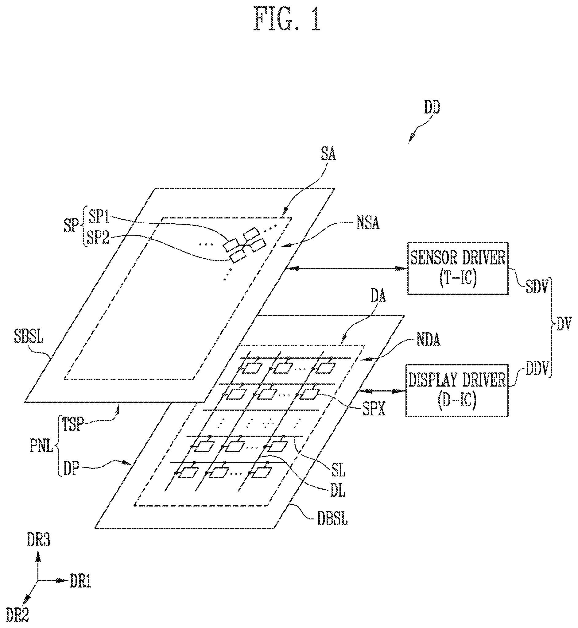
The disclosure may be modified in various manners and have various forms. Therefore, specific embodiments will be illustrated in the drawings and will be described in more detail in the specification. However, it should be understood that the disclosure is not intended to be limited to the disclosed specific forms, and the disclosure comprises all modifications, equivalents, and substitutions within the spirit and technical scope of the disclosure. Terms of “first”, “second”, and the like may be used to describe various components, but the components should not be limited by the terms. The terms are used only for the purpose of distinguishing one component from another component. For example, without departing from the scope of the disclosure, a first component May be referred to as a second component, and similarly, a second component may also be referred to as a first component. In the following description, the singular expressions comprise plural expressions unless the context clearly dictates otherwise. It should be understood that in the present application, a term of “comprise”, “have”, or the like is used to specify that there is a feature, a number, a step, an operation, a component, a part, or a combination thereof described in the specification, but does not exclude a possibility of the presence or addition of one or more other features, numbers, steps, operations, components, parts, or combinations thereof in advance. In addition, a case where a portion of a layer, a layer, an area, a plate, or the like is referred to as being “on” another portion, it comprises not only a case where the portion is “directly on” another portion, but also a case where there is further another portion between the portion and another portion. In addition, in the present specification, when a portion of a layer, a layer, an area, a plate, or the like is formed on another portion, a forming direction is not limited to an upper direction but comprises forming the portion on a side surface or in a lower direction. On the contrary, when a portion of a layer, a layer, an area, a plate, or the like is formed “under” another portion, this comprises not only a case where the portion is “directly beneath” another portion but also a case where there is further another portion between the portion and another portion. Aspects of some embodiments of the present disclosure relate to a display device comprising a touch sensor. Hereinafter, a display device comprising a touch sensor according to some embodiments is described with reference to the accompanying drawings. is a diagram illustrating a display device according to some embodiments. is a schematic cross-sectional view illustrating a stack structure of a display device according to some embodiments. Referring to , the display device DD is configured to provide (or emit) light and/or display images. The display device DD may include a panel PNL and a driving circuit unit DV for driving the panel PNL. The display device DD may further include an outer part OUP. The panel PNL may comprise a display part (or display or display panel) DP for displaying images and a sensor part TSP capable of sensing a user input (for example, a touch input, e.g., from a user's finger or a stylus). The display part DP may be referred to as a display panel. The sensor part (or sensor or sensing panel) TSP may be referred to as a sensing panel. The panel PNL may comprise sub-pixels SPX and sensing electrodes SP. According to some embodiments, the sub-pixels SPX may collectively display images in a display frame period unit. The sensing electrodes SP may sense an input (for example, a touch input) of a user in a sensing frame period unit. A sensing frame period and a display frame period may be independent of each other or may be different from each other. The sensing frame period and the display frame period May be synchronized with each other or may be asynchronous. The sensor part TSP comprising the sensing electrodes SP may obtain information from or based on the touch input of the user. According to some embodiments (for example, a mutual capacitance method), the sensing electrodes SP may comprise a first sensing electrode SP 1 providing a first sensing signal and a second sensing electrode SP 2 providing a second sensing signal. According to some embodiments, the first sensing electrode SP 1 may be a Tx (transmitter) pattern electrode, and the second sensing electrode SP 2 may be an Rx (receiver) pattern electrode. The information on the touch input (or a touch event) may mean information comprising a position or the like of a touch that the user wants to provide. However, embodiments according to the present disclosure are not limited thereto. For example, according to some embodiments (for example, a self-capacitance method), the sensing electrodes SP may be configured of one type of sensing electrodes without distinction between the first sensing electrode SP 1 and the second sensing electrode SP 2 . The driving circuit unit DV may comprise a display driver DDV for driving the display part DP and a sensor driver SDV for driving the sensor part TSP. The display part DP may comprise a display base layer DBSL and the sub-pixels SPX provided on the display base layer DBSL. The sub-pixels SPX may be located in a display area DA. The display base layer DBSL (or the display device DD) may comprise the display area DA in which images are displayed and a non-display area NDA outside the display area DA. According to some embodiments, the display area DA may be located in a central area of the display part DP, and the non-display area NDA may be located adjacent to or in a periphery (e.g., outside a footprint) of the display area DA. The display base layer DBSL may be a base substrate or a base member for supporting the display device DD. The base layer may be a rigid substrate of a glass material. Alternatively, the base layer may be a flexible substrate of which bending, folding, rolling, or the like may be performed without damaging the display device DD. In this case, the base layer may comprise an insulating material such as a polymer resin such as polyimide. However, embodiments according to the present disclosure are not particularly limited thereto. Scan lines SL and data lines DL, and the sub-pixels SPX connected to the scan lines SL and the data lines DL may be located in the display area DA. The sub-pixels SPX may be configured to be selected by a scan signal of a turn-on level supplied from the scan lines SL, receive a data signal from the data lines DL, and emit light of a luminance corresponding to the data signal. Accordingly, an image corresponding to the data signal is displayed in the display area DA. However, in the disclosure, a structure, a driving method, and the like of the sub-pixels SPX are not particularly limited. Various lines and/or built-in circuit units connected to the sub-pixels SPX of the display area NDA may be located in the non-display area NDA. For example, a plurality of lines for supplying various power and control signals to the display area DA may be located in the non-display area NDA. The display part DP may output or display visual information (for example, an image). According to some embodiments, a type/kind of the display part DP is not particularly limited. For example, the display part DP may be implemented as a self-emission type of display panel such as an organic light emitting display panel. However, when the display part DP is implemented as a self-emission type, each pixel is not limited to a case in which only an organic light emitting element is utilized. For example, a light emitting element of each pixel may be formed of an organic light emitting diode, an inorganic light emitting diode, a quantum dot/well light emitting diode, or the like. According to some embodiments, the display part DP may be implemented as a non-emission type of display panel such as a liquid crystal display panel. When the display part DP is implemented as a non-emission type, the display device DD may additionally comprise a light source such as a back-light unit. Hereinafter, for convenience of description, the disclosure is described based on some embodiments in which the display part DP is implemented as an organic light emitting display panel, but as described above, embodiments according to the present disclosure are not limited thereto. The sensor part TSP comprises a sensor base layer SBSL and a plurality of sensing electrodes SP formed on the sensor base layer SBSL. The sensing electrodes SP may be located in a sensing area SA on the sensor base layer SBSL. The sensor base layer SBSL (or the display device DD) may comprise a sensing area SA where a touch input or the like may be sensed, and a non-sensing area NSA around the sensing area SA. According to some embodiments, the sensing area SA may be arranged to overlap at least one area of the display area DA. For example, the sensing area SA may be set or formed as an area corresponding to the display area DA (for example, an area overlapping the display area DA), and the non-sensing area NSA may be set or formed as an area corresponding to the non-display area NDA (for example, an area overlapping the non-display area NDA). In this case, when the touch input or the like is provided on the display area DA, the touch input may be detected through the sensor part TSP. Embodiments according to the present disclosure are not limited thereto, however. For example, according to some embodiments, the sensing area SA may extend over at least a portion of the non-display area NDA). The sensor base layer SBSL may comprise one or more insulating layers (for example, a first insulating layer INS 1 (refer to )). For example, the first insulating layer INS 1 for forming the sensor base layer SBSL may be located on the display part DP to form a base for forming the sensing electrodes SP. However, an example for forming the sensor base layer SBSL is not particularly limited. The sensing area SA is set as an area capable of responding to the touch input (that is, an active area of a sensor). To this end, the sensing electrodes SP for sensing the touch input or the like may be located in the sensing area SA. The sensor part TSP may obtain information on an input provided from the user. The sensor part TSP may recognize the touch input. The sensor part TSP may recognize the touch input using a capacitive sensing method. The sensor part TSP may sense the touch input using a mutual capacitance method or may sense the touch input using a self-capacitance method. According to some embodiments, each of the first sensing electrodes SP 1 may extend in a first direction DR 1 . The first sensing electrodes SP 1 may be arranged in a second direction DR 2 . The second direction DR 2 may be different from the first direction DR 1 . For example, the second direction DR 2 may be a direction perpendicular to the first direction DR 1 . According to some embodiments, each of the second sensing electrodes SP 2 may extend in the second direction DR 2 . The second sensing electrodes SP 2 may be arranged in the first direction DR 1 . According to some embodiments, the first sensing electrodes SP 1 and the second sensing electrodes SP 2 may have the same (for example, substantially the same) shape. For example, the first sensing electrodes SP 1 which are Tx patterns and the second sensing electrodes SP 2 which are Rx patterns may have corresponding shapes (for example, the same or substantially the same shape), and thus sensing performance of the touch event may be uniformly set within the sensing area SA. Meanwhile, sensing lines for electrically connecting the sensing electrodes SP to the sensor driver SDV and the like may be located in the non-sensing area NSA of the sensor part TSP. The driving circuit unit DV may comprise a display driver DDV for driving the display part DP and a sensor driver SDV for driving the sensor part TSP. The display driver DDV is configured to be electrically connected to the display part DP to drive the sub-pixels SPX. The sensor driver SDV is configured to be electrically connected to the sensor part TSP to drive the sensor part TSP. The outer part OUP may be substantially located outside the display device DD. The outer part OUP may be located on the sensor part TSP. Light provided from the display part DP may pass through the outer part OUP and may be output to the outside. According to some embodiments, the outer part OUP may comprise a window. According to some embodiments, the outer part OUP may comprise a reflection control layer RCL (refer to ) and a light blocking layer LBL (refer to ). According to some embodiments, the outer part OUP may comprise color filters CF 1 , CF 2 , and CF 3 (refer to ). Next, referring to , aspects of the display part DP according to some embodiments is described. is a schematic cross-sectional view illustrating a display part according to some embodiments. Referring to , the display part DP may comprise a pixel circuit layer PCL and a light emitting element layer EML. The pixel circuit layer PCL may comprise a pixel circuit for driving light emitting elements LD. The pixel circuit layer PCL may comprise the display base layer DBSL, conductive layers for forming pixel circuits, and insulating layers located between the conductive layers. The pixel circuit may comprise a thin film transistor. The pixel circuit may comprise a driving transistor. The pixel circuit may be electrically connected to the light emitting elements LD to provide an electrical signal for the light emitting elements LD to emit light. The light emitting element layer EML may be located on the pixel circuit layer PCL. According to some embodiments, the light emitting element layer EML may comprise the light emitting element LD, a pixel defining layer PDL, a low-reflection inorganic layer LRI, and an encapsulation layer TFE. The light emitting element LD may be located on the pixel circuit layer PCL. According to some embodiments, the light emitting element LD may comprise a first electrode ELT 1 , an emission layer EL, and a second electrode ELT 2 . According to some embodiments, the emission layer EL may be located in an area defined by the pixel defining layer PDL. The pixel defining layer PDL may be adjacent to a periphery of the emission layer EL. A surface of the emission layer EL may be electrically connected to the first electrode ELT 1 , and another surface of the emission layer EL may be electrically connected to the second electrode ELT 2 . The first electrode ELT 1 may be an anode electrode for the emission layer EL, and the second electrode ELT 2 may be a common electrode (or a cathode electrode) for the emission layer EL. According to some embodiments, the first electrode ELT 1 and the second electrode ELT 2 may comprise a conductive material. For example, the first electrode ELT 1 may comprise a conductive material having a reflective property, and the second electrode ELT 2 may comprise a transparent conductive material. However, embodiments according to the present disclosure are not limited thereto. The emission layer EL may have a multilayer thin film structure comprising a light generation layer. The emission layer EL may comprise a hole injection layer for injecting a hole, a hole transport layer having an excellent hole transport property and for increasing a chance of recombination of a hole and an electron by suppressing a movement of an electron that is not combined in the light generation layer, the light generation layer for emitting light by the recombination of the injected electron and hole, a hole blocking layer for suppressing a movement of a hole that is not combined in the light generation layer, an electron transport layer for smoothly transporting the electron to the light generation layer, and an electron injection layer for injecting the electron. The emission layer EL may emit light based on an electrical signal provided from the first electrode ELT 1 and the second electrode ELT 2 . The emission layer EL may form a sub-pixel SPX. The emission layer EL may form a sub-pixel area SPXA from which light of a color is emitted. In a plan view (e.g., in a view perpendicular or normal with respect to a display surface of the display device DD), an area of the emission layer EL and the sub-pixel area SPXA may correspond to each other. For example, each emission layer EL may correspond to each sub-pixel area SPXA. The pixel defining layer PDL may be located on the pixel circuit layer PCL to define a position where the emission layer EL is arranged. The pixel defining layer PDL may comprise an organic material. According to some embodiments, the pixel defining layer PDL may comprise one or more of a group of acrylic resin, epoxy resin, phenol resin, polyamide resin, and polyimide resin. However, embodiments according to the present disclosure are not limited thereto. For example, the pixel defining layer PDL may comprise an inorganic material. The low-reflection inorganic layer LRI may be located on the light emitting element LD (for example, the second electrode ELT 2 ). The low-reflection inorganic layer LRI may be located between the encapsulation layer TFE and the light emitting element LD. The low-reflection inorganic layer LRI may comprise an inorganic material. For example, the low-reflection inorganic layer LRI may comprise one or more of a metal or a metal compound in consideration of a refractive index and an absorption coefficient. The low-reflection inorganic layer LRI may absorb light applied from the outside into the display device DD and reduce an external light reflectance of the display device DD. Accordingly, display quality and visibility of the display device DD may be relatively improved by comprising the low-reflection inorganic layer LRI. The encapsulation layer TFE may be located on the low-reflection inorganic layer LRI. The encapsulation layer TFE may offset a step difference generated by the light emitting element LD, the low-reflection inorganic layer LRI, and the pixel defining layer PDL. The encapsulation layer TFE may comprise a plurality of insulating layers covering the light emitting element LD. According to some embodiments, the encapsulation layer TFE may have a structure in which an inorganic layer and an organic layer are alternately stacked. According to some embodiments, the encapsulation layer TFE may be a thin film encapsulation layer. Next, aspects of the sensor part TSP are described with reference to to 8 . is a schematic cross-sectional view illustrating a sensing unit according to some embodiments. are schematic plan views illustrating sensing electrodes according to some embodiments. show a schematic planar structure illustrating an area where the first sensing electrode SP 1 and the second sensing electrode SP 2 are adjacent to each other. show a planar structure of the first sensing electrode SP 1 and the second sensing electrode SP 2 each having one shape according to some embodiments. is a schematic cross-sectional view illustrating a sensing unit according to some embodiments. shows a schematic cross-sectional structure taken on a line A˜A′ of and a cross-sectional structure taken on a line B˜B′ of . Referring to to 7 , the sensor part TSP may be located on the encapsulation layer TFE. The sensor part TSP may comprise the first insulating layer INS 1 , a first conductive pattern layer CP 1 , a second insulating layer INS 2 , a second conductive pattern layer CP 2 , and a protective layer PVX. According to some embodiments, the first conductive pattern layer CP 1 and the second conductive pattern layer CP 2 may be patterned in an area to form the sensing electrodes SP. For example, a portion of the first conductive pattern layer CP 1 may configure the first sensing electrode SP 1 , and a portion of each of the first conductive pattern layer CP 1 and the second conductive pattern layer CP 2 may configure the second sensing electrode SP 2 . Alternatively, a portion of the second conductive pattern layer CP 2 may configure the first sensing electrode SP 1 , and a portion of each of the first conductive pattern layer CP 1 and the second conductive pattern layer CP 2 may configure the second sensing electrode SP 2 . However, embodiments according to the present disclosure are not limited thereto. The first insulating layer INS 1 may be located on the encapsulation layer TFE. The first insulating layer INS 1 may form the sensor base layer SBSL to provide an area where the first conductive pattern layer CP 1 , the second insulating layer INS 2 , the second conductive pattern layer CP 2 , and the protective layer PVX are located. The first conductive pattern layer CP 1 may be located on the first insulating layer INS 1 . The second conductive pattern layer CP 2 may be located on the second insulating layer INS 2 . The first conductive pattern layer CP 1 and the second conductive pattern layer CP 2 may be spaced apart from each other with the second insulating layer INS 2 interposed therebetween. The first conductive pattern layer CP 1 and the second conductive pattern layer CP 2 may comprise a metal layer of a single layer or multiple layers. The first conductive pattern layer CP 1 and the second conductive pattern layer CP 2 may comprise at least one of various metal materials comprising gold (Au), silver (Ag), aluminum (Al), molybdenum (Mo), chromium (Cr), titanium (Ti), nickel (Ni), neodymium (Nd), copper (Cu), or platinum (Pt), and/or an alloy thereof. According to some embodiments, the first conductive pattern layer CP 1 and the second conductive pattern layer CP 2 may comprise at least one of various transparent conductive materials comprising one of a silver nanowire (AgNW), indium tin oxide (ITO), indium zinc oxide (IZO), indium gallium zinc oxide (IGZO), antimony zinc oxide (AZO), indium tin zinc oxide (ITZO), zinc oxide (ZnO), tin oxide (SnO2), carbon nano tube, or graphene. The second insulating layer INS 2 may be located on the first conductive pattern layer CP 1 . The second insulating layer INS 2 may be interposed between the first conductive pattern layer CP 1 and the second conductive pattern layer CP 2 . The protective layer PVX may be located on the second conductive pattern layer CP 2 . The first insulating layer INS 1 may comprise one or more of an inorganic material and an organic material. The second insulating layer INS 2 may comprise one or more of an inorganic material and an organic material. According to some embodiments, the protective layer PVX may comprise an organic material. The inorganic material may comprise one or more of a group of silicon nitride (SiNx), silicon oxide (SiOx), silicon oxynitride (SiOxNy), and aluminum oxide (AlOx). The organic material may comprise one or more of a group of acrylic resin, epoxy resin, phenol resin, polyamide resin, and polyimide resin. However, embodiments according to the present disclosure are not limited thereto. According to some embodiments, when the second insulating layer INS 2 comprises an organic material, a short risk between the first conductive pattern layer CP 1 and the second conductive pattern layer CP 2 may be reduced. Accordingly, even though a thickness of at least one of the first conductive pattern layer CP 1 or the second conductive pattern layer CP 2 is increased, a structural risk may be reduced, and thus a process design freedom degree may be relatively improved. The sensing electrodes SP may comprise a cell C and a bridge BRD. The cell C may have a relatively large area, and the bridge BRD may have a relatively small area. Cells C adjacent to each other may be electrically connected by the bridge BRD. The cell C may comprise a first cell C 1 and a second cell C 2 . The bridge BRD may comprise a first bridge BRD 1 and a second bridge BRD 2 . According to some embodiments, the first cell C 1 and the second cell C 2 may be formed by the second conductive pattern layer CP 2 . The first bridge BRD 1 may be formed by the second conductive pattern layer CP 2 . A portion of the second bridge BRD 2 may be formed by the first conductive pattern layer CP 1 , and another portion of the second bridge BRD 2 may be formed by the second conductive pattern layer CP 2 . However, embodiments according to the present disclosure are not necessarily limited thereto. For example, the first cell C 1 and the second cell C 2 may be formed by the first conductive pattern layer CP 1 . The first bridge BRD 1 may be formed by the first conductive pattern layer CP 1 . A portion of the second bridge BRD 2 may be formed by the second conductive pattern layer CP 2 , and another portion of the second bridge BRD 2 may be formed by the first conductive pattern layer CP 1 . According to some embodiments, the sensing electrodes SP may have a mesh structure. The cells C and the bridges BRD may have a mesh structure. For example, the second conductive pattern layer CP 2 for forming the sensing electrodes SP may be patterned according to the mesh structure. Because the sensing electrodes SP have the mesh structure, a capacitance that may be formed with other electrodes located under the cells C may be reduced. The first sensing electrode SP 1 may have a structure in which the first cells C 1 of a relatively large area and the first bridge BRD 1 of a relatively small area are connected to each other. For example, the first cell C 1 may comprise a (1-1)-th cell C 1 - 1 and a (1-2)-th cell C 1 - 2 , and the first bridge BRD 1 may electrically connect the (1-1)-th cell C 1 - 1 and the (1-2)-th cell C 1 - 2 . The second sensing electrode SP 2 may have a structure in which the second cells C 2 of a relatively large area and the second bridge BRD 2 of a relatively small area are connected to each other. For example, the second cell C 2 may comprise a (2-1)-th cell C 2 - 1 and a (2-2)-th cell C 2 - 2 , and the second bridge BRD 2 may electrically connect the (2-1)-th cell C 2 - 1 and the (2-2)-th cell C 2 - 2 . According to some embodiments, the second bridge BRD 2 may be electrically connected to the (2-1)-th cell C 2 - 1 through a contact portion CNT and may be electrically connected to the (2-2)-th cell C 2 - 2 through the another contact portion CNT. Accordingly, the second bridge BRD 2 located on a layer different from that of the second cell C 2 may electrically connect the (2-1)-th cell C 2 - 1 and the (2-2)-th cell C 2 - 2 through the contact portion CNT. According to some embodiments, the contact portion CNT may pass through the second insulating layer INS 2 . The first cell C 1 and the second cell C 2 may generally have a diamond shape ( ). However, a shape of the first cell C 1 and the second cell C 2 is not particularly limited thereto. For example, the first cell C 1 and the second cell C 2 may have a generally quadrangular shape ( ). The first sensing electrodes SP 1 and the second sensing electrodes SP 2 may be adjacent to each other with a separating line SEL interposed therebetween. The separating line SEL may be a virtual line located in an area between the first sensing electrodes SP 1 and the second sensing electrodes SP 2 . For example, the separating line SEL may be located between the (1-1)-th cell C 1 - 1 and the (1-2)-th cell C 1 - 2 . The separating line SEL may be located between the first bridge BRD 1 and the (1-2)-th cell C 1 - 2 . Next, a cross-sectional structure of the display device DD according to some embodiments is described with reference to . are schematic cross-sectional views illustrating a display device according to some embodiments. Referring to , the emission layer EL may comprise a first emission layer EL 1 comprised in a first sub-pixel SPX 1 , a second emission layer EL 2 comprised in a second sub-pixel SPX 2 , and a third emission layer EL 3 comprised in a third sub-pixel SPX 3 . The first emission layer EL 1 may emit light of a first color (for example, red) and may form a first sub-pixel area SPXA 1 . The second emission layer EL 2 may emit light of a second color (for example, green) and may form a second sub-pixel area SPXA 2 . The third emission layer EL 3 may emit light of a third color (for example, blue) and may form a third sub-pixel area SPXA 3 . In the sensor part TSP, the first conductive pattern layer CP 1 and the second conductive pattern layer CP 2 may be located on different layers to form a structure of the sensing electrodes SP. The outer part OUP may be located on the sensor part TSP. The outer part OUP may comprise the light blocking layer LBL and the reflection control layer RCL. The light blocking layer LBL may overlap the first conductive pattern layer CP 1 and the second conductive pattern layer CP 2 in a plan view. The light blocking layer LBL may comprise a light blocking material, but embodiments according to the present disclosure are not necessarily limited thereto. The reflection control layer RCL may selectively absorb light of a wavelength range to control a reflectance and a color sense of the display device DD. According to some embodiments, the reflection control layer RCL may comprise a dye, a pigment, or a combination thereof. For example, the reflection control layer RCL may comprise one or more of a group of an oxazine-based compound, a cyanine-based compound, a tetraazoporphine-based compound, and a squarylium-based compound, but embodiments according to the present disclosure are not limited thereto. According to some embodiments, sizes (or areas) of the sub-pixel areas SPXA may be different from each other. Areas of the first sub-pixel area SPXA 1 , the second sub-pixel area SPXA 2 , and the third sub-pixel area SPXA 3 may be different from each other. For example, the area of the third sub-pixel area SPXA 3 may be greater than that of the second sub-pixel area SPXA 2 . The area of the second sub-pixel area SPXA 2 may be greater than that of the first sub-pixel area SPXA 1 . However, embodiments according to the present disclosure are not necessarily limited thereto. According to some embodiments, the area of the second sub-pixel area SPXA 2 and the area of the first sub-pixel area SPXA 1 may be equal to each other. Hereinafter, for convenience of description, aspects of some embodiments are illustrated and described in which the area of the second sub-pixel area SPXA 2 is greater than that of the first sub-pixel area SPXA 1 . According to some embodiments, a light emitting efficiency deviation for each color of the sub-pixel SPX may be compensated for by manufacturing the area of some sub-pixel areas SPXA to be different. According to some embodiments, referring to , the outer part OUP may further comprise color filters CF 1 , CF 2 , and CF 3 . According to some embodiments, as the color filters CF 1 , CF 2 , and CF 3 corresponding to colors of the respective first to third sub-pixels SPX 1 , SPX 2 , and SPX 3 are located, a full-color image may be displayed. A first color filter CF 1 may overlap the first sub-pixel area SPXA 1 in a plan view as a color filter for forming a first sub-pixel SPX 1 . The first color filter CF 1 May selectively transmit the light of the first color. The first color filter CF 1 may comprise a red color filter material as a red color filter. A second color filter CF 2 may overlap a second sub-pixel area SPXA 2 in a plan view as a color filter for forming a second sub-pixel SPX 2 . The second color filter CF 2 may selectively transmit the light of the second color. The second color filter CF 2 may comprise a green color filter material as a green color filter. A third color filter CF 3 may overlap a third sub-pixel area SPXA 3 in a plan view as a color filter for forming a third sub-pixel SPX 3 . The third color filter CF 3 may selectively transmit the light of the third color. The third color filter CF 3 may comprise a blue color filter material as a blue color filter. The cross-sectional structure of the display device DD according to some embodiments is not necessarily limited to the above-described example. Hereinafter, a structure of the first conductive pattern layer CP 1 , the second conductive pattern layer CP 2 , and the sub-pixels SPX of the display device DD according to some embodiments is described with reference to to 22 . A content that may overlap the above-described content is simplified or is not repeated. First, the display device DD according to some embodiments is described with reference to to 19 . In the display device DD as illustrated and described with respect to to 19 , the cells C may be formed by the second conductive pattern layer CP 2 . to 19 are schematic diagrams illustrating the display device DD according to some embodiments. to 13 , 18 , and 19 are schematic plan views illustrating the display device according to some embodiments. to 17 are schematic cross-sectional views illustrating the display device according to some embodiments. may be schematic plan views illustrating the sub-pixel areas SPXA, the first conductive pattern layer CP 1 , and the second conductive pattern layer CP 2 . show the sub-pixels SPX 1 , SPX 2 , and SPX 3 (or the emission layers EL 1 , EL 2 , and EL 3 ) forming the sub-pixel areas SPXA 1 , SPXA 2 , and SPXA 3 , and show the conductive pattern layers CP 1 and CP 2 formed around the sub-pixel areas SPXA. schematically shows adjacent pixels PXL 1 and PXL 2 based on an area where the second bridge BRD 2 is located. is a plan view illustrating a display device DD according to some embodiments, and shows the sensing electrodes SP and the separating line SEL. omits the sub-pixels SPX 1 , SPX 2 , and SPX 3 so that a relationship between the sensing electrodes SP and the separating line SEL may be more clearly understood. may show the same area as , and thus a positional relationship between the sensing electrodes SP and the separating line SEL and the sub-pixels SPX 1 , SPX 2 , and SPX 3 will be clearly understood. Referring to to 13 , each of the sub-pixels SPX according to some embodiments may be arranged according to one structure. For example, the sub-pixels SPX may be arranged according to an S-stripe structure. In the following description, a positional relationship of the sub-pixels SPX 1 , SPX 2 , and SPX 3 may correspond to a positional relationship of the sub-pixel areas SPXA 1 , SPXA 2 , and SPXA 3 and/or the emission layers EL 1 , EL 2 , and EL 3 . The first sub-pixel SPX 1 and the second sub-pixel SPX 2 may form a first pixel column COL 1 . The first sub-pixel SPX 1 and the second sub-pixel SPX 2 may be sequentially located on the first direction DR 1 . The first sub-pixel SPX 1 and the second sub-pixel SPX 2 may be alternately arranged on the first direction DR 1 . The first sub-pixel SPX 1 and the second sub-pixel SPX 2 may be located in the first pixel column COL 1 without the third sub-pixel SPX 3 . The third sub-pixel SPX 3 may form a second pixel column COL 2 . The third sub-pixel SPX 3 may be sequentially located on the first direction DR 1 . The third sub-pixel SPX 3 may be located in the second pixel column COL 2 without the first sub-pixel SPX 1 and the second sub-pixel SPX 2 . According to some embodiments, the third sub-pixels SPX 3 may be spaced apart by a first distance in a first area A 1 , and other third sub-pixels SPX 3 may be spaced apart by a second distance greater than the first distance in a second area A 2 adjacent to the first direction DR 1 in the first direction DR 1 ( ). However, embodiments according to the present disclosure are not necessarily limited thereto. The third sub-pixels SPX 3 may be spaced apart from each other at a uniform distance on the first direction DR 1 ( ). The first pixel column COL 1 and the second pixel column COL 2 may be adjacent to each other on the second direction DR 2 . For example, the first sub-pixel SPX 1 may be adjacent to the third sub-pixel SPX 3 on the second direction DR 2 . The second sub-pixel SPX 2 may be adjacent to the third sub-pixel SPX 3 on the second direction DR 2 . The first pixel column COL 1 and the second pixel column COL 2 may be alternately arranged on the second direction DR 2 . For example, the second pixel column COL 2 may be located between two first pixel columns COL 1 . The first pixel column COL 1 may be located between two second pixel columns COL 2 . The first sub-pixel SPX 1 and the second sub-pixel SPX 3 adjacent to each other on the first direction DR 1 may form the pixel PXL (or a pixel unit) with the third sub-pixel SPX 3 adjacent on the second direction DR 2 . For example, the first to third sub-pixels SPX 1 , SPX 2 , and SPX 3 may form a first pixel PXL 1 , and the first to third sub-pixels SPX 1 , SPX 2 , and SPX 3 may form a second pixel PXL 2 in an area adjacent to the first pixel PXL 1 in the first direction DR 1 . The pixels PXL may be sequentially arranged on the first direction DR 1 and the second direction DR 2 . According to some embodiments, the first sensing electrode SP 1 and the second sensing electrode SP 2 may be located adjacent to the sub-pixel areas SPXA. For example, the first sensing electrode SP 1 and the second sensing electrode SP 2 may be spaced apart from each other based on the separating line SEL. For example, the second cell C 2 may be spaced apart from the first cell C 1 with the separating line SEL interposed therebetween. The second cell C 2 may be spaced apart from the first bridge BRD 1 with the separating line SEL interposed therebetween. The second conductive pattern layer CP 2 may be arranged around the sub-pixel SPX (or the sub-pixel areas SPXA). The second conductive pattern layer CP 2 may surround at least a portion of the sub-pixel areas SPXA in a plan view. The second conductive pattern layer CP 2 may be arranged around the sub-pixel SPX to prevent light emitting efficiency from being reduced and minimize damage to external visibility. The light blocking layer LBL and the pixel defining layer PDL may be arranged around the sub-pixel SPX. For example, the second conductive pattern layer CP 2 may be arranged to overlap the light blocking layer LBL and the pixel defining layer PDL. According to some embodiments, at least a portion of the second conductive pattern layer CP 2 may form a loop (for example, a closed loop or an open loop) surrounding one or more of the sub-pixel areas SPXA. Accordingly, the second conductive pattern layer CP 2 may form a mesh structure. According to some embodiments, at least a portion of the second conductive pattern layer CP 2 may be disconnected at the separating line SEL. This is described with reference to . is a schematic cross-sectional view taken on a line C˜C′ of . Referring to together, the first sensing electrode SP 1 and the second sensing electrode SP 2 may be spaced apart from each other with the separating line SEL interposed therebetween. Since the second conductive pattern layers CP 2 are electrically separated from each other with the separating line SEL interposed therebetween, the first sensing electrode SP 1 and the second sensing electrode SP 2 to which different sensing signals may be supplied may be defined. At least a portion of the separating line SEL may extend on the first direction DR 1 and pass through the first sub-pixel SPX 1 and the second sub-pixel SPX 2 . For example, at least a portion of the separating line SEL may extend in the first direction DR 1 , and may pass through the first sub-pixel SPX 1 and the second sub-pixel SPX 1 of each of the first pixel PXL 1 and the second pixel PXL 2 . For example, the separating line SEL may overlap the first sub-pixel SPX 1 and the second sub-pixel SPX 2 in a plan view. A portion of the separating line SEL may be located over the first sub-pixel SPX 1 and the second sub-pixel SPX 2 of the first pixel PXL 1 and the first sub-pixel SPX 1 and the second sub-pixel SPX 2 of the second pixel PXL 2 . According to some embodiments, the separating line SEL may not overlap the second bridge BRD 2 in a plan view. The separating line SEL may not overlap an additional bridge BRD 2 ′ in a plan view. For example, a portion of the separating line SEL may be located on a side of the second bridge BRD 2 , and another portion of the separating line SEL may be located on another side of the second bridge BRD 2 . Meanwhile, according to some embodiments, the first conductive pattern layer CP 1 may form the second bridge BRD 2 . A technical feature of the second bridge BRD 2 is described with reference to to 17 together. is a schematic cross-sectional view taken on a line D-D′ of . is a schematic cross-sectional view taken on a line E-E′ of . is a schematic cross-sectional view taken on a line F-F′ of . The second bridge BRD 2 may electrically connect the (2-1)-th cell C 2 - 1 and the (2-2)-th cell C 2 - 2 . For example, the second bridge BRD 2 formed by the first conductive pattern layer CP 1 may be electrically connected to a portion of the second sensing electrode SP 2 (for example, the second bridge BRD 2 formed by the second conductive pattern layer CP 2 ) through the contact portion CNT. Accordingly, the second bridge BRD 2 may electrically connect adjacent second sensing electrodes SP 2 to each other. The second bridge BRD 2 may extend in a direction in which the (2-1)-th cell C 2 - 1 and the (2-2)-th cell C 2 - 2 are spaced apart from each other. For example, the second bridge BRD 2 may extend on the second direction DR 2 . According to some embodiments, two or more second bridges BRD 2 may be provided, and may electrically connect the second sensing electrodes SP 2 adjacent to each other (for example, the (2-1)-th cell C 2 - 1 and the (2-2)-th cell C 2 - 2 ) at two or more positions. However, embodiments according to the present disclosure are not limited thereto. According to some embodiments, the second bridge BRD 2 may extend in the first direction DR 1 , and at least a portion of the second bridge BRD 2 may extend in the first direction DR 1 . According to some embodiments, the display device DD may further comprise the additional bridge BRD 2 ′. The additional bridge BRD 2 ′ may be located in an area where the cell C is formed. The additional bridge BRD 2 ′ may be located on the same layer as the second bridge BRD 2 . The additional bridge BRD 2 ′ may have a structure corresponding to the second bridge BRD 2 . For example, the additional bridge BRD 2 ′ may have the same shape as the second bridge BRD 2 . The additional bridge BRD 2 ′ may have the same length as the second bridge BRD 2 . The additional bridge BRD 2 ′ may have the same width as the second bridge BRD 2 . The additional bridge BRD 2 ′ may be electrically connected to the second conductive pattern layer CP 2 forming the sensing electrodes SP. For example, the additional bridge BRD 2 ′ may be electrically connected to the second conductive pattern layer CP 2 forming the cell C through an additional contact portion CNT′. The additional bridge BRD 2 ′ may comprise a plurality of additional bridges, and a distance at which the plurality of additional bridges are spaced apart from each other in the first direction DR 1 may be the same as a distance at which the second bridges BRD 2 are spaced apart from each other on the first direction DR 1 . Accordingly, a structure corresponding to the second bridge BRD 2 may be formed entirely in the sensing area SA. In this case, similarly to a case where the second bridge BRD 2 is not formed in a localized position but is located entirely in the sensing area SA, a risk of damage to visibility may be reduced. The second bridge BRD 2 may pass between third sub-pixels SPX 3 adjacent to each other. For example, at least another portion of the second bridge BRD 2 may be located between the third sub-pixels SPX 3 adjacent to each other. According to some embodiments, at least another portion of the second bridge BRD 2 may be located between the third sub-pixel SPX 3 of the first pixel PXL 1 and the third sub-pixel SPX 3 of the second pixel PXL 2 . The second bridge BRD 2 may not pass between the first sub-pixel SPX 1 and the second sub-pixel SPX 2 . For example, the second bridge BRD 2 may not be located between the first sub-pixel SPX 1 and the second sub-pixel SPX 2 . According to some embodiments, the second bridge BRD 2 may not be located between the first sub-pixel SPX 1 of the first pixel PXL 1 and the second sub-pixel SPX 2 of the second pixel PXL 2 . According to some embodiments, the second bridge BRD 2 may be arranged to overlap the pixel defining layer PDL having a relatively large width on the first direction DR 1 . For example, the pixel defining layer PDL may comprise a first pixel defining layer PDL 1 having a first width W 1 and a second pixel defining layer PDL 2 having a second width W 2 . The second width W 2 may be greater than the first width W 1 . According to some embodiments, the first width W 1 and the second width W 2 may be widths of each of the first pixel defining layer PDL 1 and the second pixel defining layer PDL 2 on the first direction DR 1 . Accordingly, a separation distance between the emission layers EL in the first pixel column COL 1 may be less than a separation distance between the emission layers EL in the second pixel column COL 2 . Each of the first pixel defining layer PDL 1 and the second pixel defining layer PDL 2 may be integrally formed as a portion of the pixel defining layer PDL. The first pixel defining layer PDL 1 and the second pixel defining layer PDL 2 may be spaced apart from each other on the second direction DR 2 . For example, the first pixel defining layer PDL 1 and the second pixel defining layer PDL 2 may be spaced apart in a direction different from a direction in which the first sub-pixel SPX 1 and the second sub-pixel SPX 2 are spaced apart from each other. The first pixel defining layer PDL 1 and the second pixel defining layer PDL 2 may be spaced apart in a direction in which the first sub-pixel SPX 1 and the second sub-pixel SPX 2 are spaced apart from the third sub-pixel SPX 3 . The first pixel defining layer PDL 1 may overlap the first sub-pixel SPX 1 and the second sub-pixel SPX 2 on the first direction DR 1 . The second pixel defining layer PDL 2 may overlap the third sub-pixel SPX 3 on the first direction DR 1 . According to some embodiments, the second bridge BRD 2 may be selectively located on the second pixel defining layer PDL 2 having a relatively wide width. For example, the second bridge BRD 2 may overlap the second pixel defining layer PDL 2 in a plan view. The second bridge BRD 2 may not overlap the first pixel defining layer PDL 1 in a plan view. In this case, the conductive pattern layers CP 1 and CP 2 may be entirely comprised in an area where the pixel defining layer PDL is located in a plan view, but an edge area EDG of the pixel defining layer PDL where the conductive pattern layers CP 1 and CP 2 are not located may be defined larger. The edge area EDG of the pixel defining layer PDL may be an area adjacent to (for example, directly adjacent to) the emission layer EL, and may be an area which does not overlap the conductive pattern layers CP 1 and CP 2 in a plan view. Experimentally, when the edge area EDG of the pixel defining layer PDL is manufactured to be excessively narrow, a risk that light emitted from the emission layer EL may be interfered with by the conductive pattern layers CP 1 and CP 2 may occur. However, according to some embodiments, since the second bridge BRD 2 is located on the second pixel defining layer PDL 2 having the relatively wide second width W 2 and is not be located on the first pixel defining layer PDL 1 having the relatively narrow first width W 1 , the edge area EDG may be secured widely. Accordingly, a risk of occurrence of a light occlusion phenomenon in which a path of the emitted light is covered by the conductive pattern layers CP 1 and CP 2 may be reduced. As a result, light emission efficiency of the display device DD may be relatively improved, and the display device DD with relatively improved visibility may be provided. In particular, since a viewing angle of the emission layer EL may be determined relatively freely, the freedom degree of a process design of the display device DD may be relatively improved. According to some embodiments, the contact portion CNT may not overlap the sub-pixels SPX on the first direction DR 1 . For example, the contact portion CNT may be located between the first pixel column COL 1 and the second pixel column COL 2 . Accordingly, the second bridge BRD 2 may not overlap the first pixel column COL 1 on the first direction DR 1 . According to some embodiments, the second bridge BRD 2 may have a structure that generally extends in a direction (for example, the second direction DR 2 ) in a plan view. According to some embodiments, the second bridge BRD 2 may have a linear structure extending in the second direction DR 2 rather than a mesh structure. In some embodiments, the second bridge BRD 2 may have a structure extending in a direction without comprising a bent area in a plan view. In this case, the second bridge BRD 2 may connect the contact portion CNT for the second sensing electrode SP 2 located on a side and the contact portion CNT for the second sensing electrode SP 2 located on a side at the shortest distance. Meanwhile, referring to , the cells C according to some embodiments may further comprise a cutting area CL. are plan views illustrating a display device DD according to some embodiments, and show the sensing electrodes SP and the cutting area CL. may show the sensing electrodes SP and the cutting area CL, and may further show the sub-pixels SPX, and shows the sensing electrodes SP and the cutting area CL, and omits the sub-pixels SPX for convenience of illustration, but embodiments are not limited thereto. According to some embodiments, the cutting area CL may be an area where the second conductive pattern layer CP 2 is disconnected. For example, at least a portion of the second conductive pattern layer CP 2 may be disconnected in an area where the cells C are defined. For example, a portion of the second conductive pattern layer CP 2 and another portion of the second conductive pattern layer CP 2 may be spaced apart from each other with the cutting area CL interposed therebetween. The cutting area CL may not overlap the second bridge BRD 2 and the additional bridge BRD 2 ′ in a plan view. Accordingly, the second bridge BRD 2 and the additional bridge BRD 2 ′ may form a repetitive pattern structure in the sensing area SA. A portion of the cutting area CL may be bent to comprise one or more cutting portions. According to some embodiments, the cutting area CL may be formed in an area where the cells C are formed, and thus visibility may be relatively further improved. For example, when only the separating line SEL is formed locally, external visibility may be damaged due to a difference of an electrode arrangement structure, but the cutting area CL corresponding to a structure of the separating line SEL may be formed in the cells C, and thus light reflection may occur similarly to a substantially uniform electrode arrangement structure. Accordingly, a risk of damage to external visibility may be reduced. Next, a display device DD according to some embodiments is described with reference to to 22 . The display device DD according to some embodiments as illustrated in is different the display device DD according some embodiments as illustrated in in that the first conductive pattern layer CP 1 forms the cell C and the second conductive pattern layer CP 2 forms the second bridge BRD 2 . A content that may overlap the above-described content may be simplified or may not be repeated. to 22 are schematic diagrams illustrating the display device DD according to some embodiments. is a schematic plan view illustrating the display device according to some embodiments. are schematic cross-sectional views illustrating the display device according to some embodiments. is a schematic cross-sectional view taken on a line G˜G′ of . is a schematic cross-sectional view taken on a line H˜H′ of . may indicate a technical feature corresponding to . may indicate a technical feature corresponding to . Among the technical features described with respect to , the features of the first conductive pattern layer CP 1 may correspond to the features of the second conductive pattern layer CP 2 as illustrated and described with respect to , and the features of the second conductive pattern layer CP 2 may correspond to the features of the first conductive pattern layer CP 1 as illustrated and described with respect to . For example, as illustrated in , the first cell C 1 and the second cell C 2 may be formed by the first conductive pattern layer CP 1 . The first bridge BRD 1 may be formed by the first conductive pattern layer CP 1 . A portion of the second bridge BRD 2 may be formed by the second conductive pattern layer CP 2 , and another portion of the second bridge BRD 2 may be formed by the first conductive pattern layer CP 1 . According to some embodiments, the second bridge BRD 2 may be formed by the second conductive pattern layer CP 2 and may overlap the second pixel defining layer PDL 2 in a plan view. The second bridge BRD 2 may overlap the first pixel defining layer PDL 1 in a plan view. According to some embodiments, the second bridge BRD 2 formed by the second conductive pattern layer CP 2 may electrically connect the second sensing electrodes SP 2 adjacent to each other (for example, the second bridges BRD 2 formed by the first conductive pattern layer CP 1 ). According to some embodiments, the second bridge BRD 2 may be formed by the second conductive pattern layer CP 2 relatively located at an upper portion, and may overlap the second pixel defining layer PDL 2 having the second width W 2 . In this case, the edge area EDG of the pixel defining layer PDL may be secured widely, and a risk that the path of the light emitted from the emission layer EL is interfered with by the second bridge BRD 2 may be further reduced. For example, the light emitted from the emission layer EL may be emitted in an upper direction (for example, in a third direction DR 3 ). At this time, the emitted light may be provided on a light path having one angle with respect to a base layer BSL. At this time, when the second conductive pattern layer CP 2 located at a relatively upper portion is not sufficiently spaced apart from the edge area EDG of the pixel defining layer PDL, a concern that the light path may be interfered with may exist. However, according to some embodiments, the second bridge BRD 2 located at a relatively upper portion is selectively located on the second pixel defining layer PDL 2 having the relatively wide second width W 2 , and thus the second conductive pattern layer CP 2 may be sufficiently spaced apart from ends of the second pixel defining layer PDL 2 . Accordingly, the concern that the light path May be interfered with may be reduced, and as a result, light emission efficiency of the display device DD may be relatively improved. As described above, although aspects of some embodiments of the disclosure have been described with reference to the example embodiments illustrated and described above, those skilled in the art or those having a common knowledge in the art will understand that the disclosure may be variously modified and changed without departing from the spirit and technical area of the disclosure as defined in the appended claims and their equivalents. Therefore, the technical scope of the disclosure should not be limited to the contents described in the detailed description of the specification, but should be defined by the claims, and their equivalents.
Figures (20)
Citations
This patent cites (8)
- US11023058
- US2014/0285729
- US2017/0364175
- US2018/0033832
- US2020/0295092
- US2021/0200365
- US2022/0029138
- US10-2392171