Multi-foldable Electronic Device Including a Plate Arrangement
Abstract
Disclosed is an electronic device including a display module, a window above the display module and including a bottom surface facing the display module, and a top surface opposite to the bottom surface, a lower film below the display module, a plate below the lower film and including a first non-folding part, a first folding part, a second non-folding part, a second folding part, and a third non-folding part that are sequentially arranged, the first folding part being configured to be folded with a first curvature and defining first holes, and the second folding part being configured to be folded with a second curvature that is different from the first curvature and defining second holes, and a first adhesion layer between the window and the plate, and defining a first opening that overlaps the first folding part and some of the first holes.
Claims (20)
1 . An electronic device, comprising: a display module; a window above the display module and comprising a bottom surface facing the display module, and a top surface opposite to the bottom surface; a lower film below the display module; a plate below the lower film and comprising a first non-folding part, a first folding part, a second non-folding part, a second folding part, and a third non-folding part that are sequentially arranged, the first folding part being configured to be folded with a first curvature and defining first holes, and the second folding part being configured to be folded with a second curvature that is different from the first curvature and defining second holes; and a first adhesion layer between the window and the plate, and defining a first opening that overlaps the first folding part and some of the first holes, the first opening being spaced apart from the remaining first holes in a plan view.
Show 19 dependent claims
2 . The electronic device of claim 1 , wherein, in a folding mode: the first folding part is configured to be folded such that the top surface of the window that overlaps the first non-folding part faces the top surface of the window that overlaps the second non-folding part; the second folding part is configured to be folded such that the bottom surface of the window that overlaps the second non-folding part faces the bottom surface of the window that overlaps the third non-folding part; and the first curvature is greater than the second curvature.
3 . The electronic device of claim 2 , wherein the first opening extends from an area over one of the first holes nearest the first non-folding part to an area over one of the first holes that overlaps a region at or near a center of the first folding part.
4 . The electronic device of claim 2 , wherein the first folding part comprises: a first side curvature part that extends from the first non-folding part; a second side curvature part that extends from the second non-folding part; a main curvature part between the first side curvature part and the second side curvature part, and defining the first holes; a first flat part between the first side curvature part and the main curvature part; and a second flat part between the second side curvature part and the main curvature part, wherein a center of curvature of the main curvature part is above the top surface of the window, and wherein a center of curvature of each of the first and second side curvature parts is below the bottom surface of the window.
5 . The electronic device of claim 4 , wherein the plate defines: first side holes that overlap the first side curvature part, and that partially penetrate from a bottom surface of the plate; and second side holes that overlap the second side curvature part, and that partially penetrate from the bottom surface of the plate.
6 . The electronic device of claim 5 , wherein the first opening extends from an area over one of the first side holes nearest the first non-folding part to an area over one of the first holes that overlaps a region at or near a center of the main curvature part.
7 . The electronic device of claim 5 , wherein the first opening extends from an area over the first flat part near the first side curvature part to an area over one of the first holes that overlaps a region at or near a center of the main curvature part.
8 . The electronic device of claim 5 , wherein the first opening extends from an area over one of the first holes nearest the first flat part to an area over one of the first holes that overlaps a region at or near a center of the main curvature part.
9 . The electronic device of claim 1 , wherein, in a folding mode: the first folding part is configured to be folded such that the top surface of the window that overlaps the first non-folding part faces the top surface of the window that overlaps the second non-folding part; the second folding part is configured to be folded such that the bottom surface of the window that overlaps the first non-folding part faces the top surface of the window that overlaps the third non-folding part; and the first curvature is greater than the second curvature.
10 . The electronic device of claim 9 , wherein the first opening extends from an area over one of the first holes nearest the first non-folding part to an area over one of the first holes that overlaps a region at or near a center of the first folding part.
11 . The electronic device of claim 9 , wherein the first folding part comprises: a first side curvature part that extends from the first non-folding part; a second side curvature part that extends from the second non-folding part; a main curvature part between the first side curvature part and the second side curvature part; a first flat part between the first side curvature part and the main curvature part; and a second flat part between the second side curvature part and the main curvature part, wherein a center of curvature of the main curvature part is above the top surface of the window, and wherein a center of curvature of each of the first and second side curvature parts is below the bottom surface of the window.
12 . The electronic device of claim 11 , wherein the plate defines: first side holes that overlap the first side curvature part, and that penetrate a portion of the plate; and second side holes that overlap the second side curvature part, and that penetrate a portion of the plate.
13 . The electronic device of claim 12 , wherein the first opening extends from an area over one of the second side holes nearest the second non-folding part to an area over one of the first holes that overlaps a region at or near a center of the main curvature part.
14 . The electronic device of claim 12 , wherein the first opening extends from an area over the second flat part near the second side curvature part to an area over one of the first holes that overlaps a region at or near a center of the main curvature part.
15 . The electronic device of claim 12 , wherein the first opening extends from an area over one of the first holes nearest the second flat part to an area over one of the first holes that overlaps a region at or near a center of the main curvature part.
16 . The electronic device of claim 9 , wherein the first adhesion layer defines a second opening that overlaps the second folding part and some of the second holes, and that extends from an area over one of the second holes nearest the second non-folding part to an area over one of the second holes that overlaps a region at or near a center of the second folding part.
17 . The electronic device of claim 1 , further comprising a second adhesion layer between the display module and the lower film, wherein the second adhesion layer defines an additional opening that overlaps the first opening, and wherein the first adhesion layer is between the lower film and the plate.
18 . The electronic device of claim 1 , further comprising a third adhesion layer below the plate, and defining a third opening that overlaps the first holes, and a fourth opening that overlaps the second holes.
19 . The electronic device of claim 1 , wherein the plate comprises a stainless steel or a fiber-reinforced composite material.
20 . The electronic device of claim 1 , further comprising an upper film between the window and the display module, and comprising a synthetic resin.
Full Description
Show full text →
CROSS-REFERENCE TO RELATED APPLICATION
This application claims priority to, and the benefit of, Korean Patent Application No. 10-2022-0098611 filed on Aug. 8, 2022, in the Korean Intellectual Property Office, the disclosure of which is hereby incorporated by reference in its entirety.
BACKGROUND
1. Field
Embodiments of the present disclosure relate to a foldable electronic device, and to an electronic device that includes an adhesion layer capable of increasing folding properties.
2. Description of the Related Art
Various types of electronic devices provide image information, and there have recently been developed electronic devices including foldable or bendable flexible display modules. Unlike rigid electronic devices, flexible electronic devices may be changed in various shapes such as being folded, rolled, or bent so that the flexible electronic devices have portable characteristics irrespective of screen sizes.
Such flexible electronic device has been studied to reduce stress applied to its components when being folded or bent.
SUMMARY
One or more embodiments provide an electronic device whose folding region has improved flexibility.
According to one or more embodiments, an electronic device includes a display module, a window above the display module and including a bottom surface facing the display module, and a top surface opposite to the bottom surface, a lower film below the display module, a plate below the lower film and including a first non-folding part, a first folding part, a second non-folding part, a second folding part, and a third non-folding part that are sequentially arranged, the first folding part being configured to be folded with a first curvature and defining first holes, and the second folding part being configured to be folded with a second curvature that is different from the first curvature and defining second holes, and a first adhesion layer between the window and the plate, and defining a first opening that overlaps the first folding part and some of the first holes.
In a folding mode, the first folding part may be configured to be folded such that the top surface of the window that overlaps the first non-folding part faces the top surface of the window that overlaps the second non-folding part, the second folding part may be configured to be folded such that the bottom surface of the window that overlaps the second non-folding part faces the bottom surface of the window that overlaps the third non-folding part, and the first curvature may be greater than the second curvature.
The first opening may extend from an area over one of the first holes nearest the first non-folding part to an area over one of the first holes that overlaps a region at or near a center of the first folding part.
The first folding part may include a first side curvature part that extends from the first non-folding part, a second side curvature part that extends from the second non-folding part, a main curvature part between the first side curvature part and the second side curvature part, and defining the first holes, a first flat part between the first side curvature part and the main curvature part, and a second flat part between the second side curvature part and the main curvature part, wherein a center of curvature of the main curvature part is above the top surface of the window, and wherein a center of curvature of each of the first and second side curvature parts is below the bottom surface of the window.
The plate may define first side holes that overlap the first side curvature part, and that partially penetrate from a bottom surface of the plate, and second side holes that overlap the second side curvature part, and that partially penetrate from the bottom surface of the plate.
The first opening may extend from an area over one of the first side holes nearest the first non-folding part to an area over one of the first holes that overlaps a region at or near a center of the main curvature part.
The first opening may extend from an area over the first flat part near the first side curvature part to an area over one of the first holes that overlaps a region at or near a center of the main curvature part.
The first opening may extend from an area over one of the first holes nearest the first flat part to an area over one of the first holes that overlaps a region at or near a center of the main curvature part.
In a folding mode the first folding part may be configured to be folded such that the top surface of the window that overlaps the first non-folding part faces the top surface of the window that overlaps the second non-folding part, the second folding part may be configured to be folded such that the bottom surface of the window that overlaps the first non-folding part faces the top surface of the window that overlaps the third non-folding part, and the first curvature may be greater than the second curvature.
The first opening may extend from an area over one of the first holes nearest the first non-folding part to an area over one of the first holes that overlaps a region at or near a center of the first folding part.
The first folding part may include a first side curvature part that extends from the first non-folding part, a second side curvature part that extends from the second non-folding part, a main curvature part between the first side curvature part and the second side curvature part, a first flat part between the first side curvature part and the main curvature part, and a second flat part between the second side curvature part and the main curvature part, wherein a center of curvature of the main curvature part is above the top surface of the window, and wherein a center of curvature of each of the first and second side curvature parts is below the bottom surface of the window.
The plate may define first side holes that overlap the first side curvature part, and that penetrate a portion of the plate, and second side holes that overlap the second side curvature part, and that penetrate a portion of the plate.
The first opening may extend from an area over one of the second side holes nearest the second non-folding part to an area over one of the first holes that overlaps a region at or near a center of the main curvature part.
The first opening may extend from an area over the second flat part near the second side curvature part to an area over one of the first holes that overlaps a region at or near a center of the main curvature part.
The first opening may extend from an area over one of the first holes nearest the second flat part to an area over one of the first holes that overlaps a region at or near a center of the main curvature part.
The first adhesion layer may define a second opening that overlaps the second folding part and some of the second holes, and that extends from an area over one of the second holes nearest the second non-folding part to an area over one of the second holes that overlaps a region at or near a center of the second folding part.
The electronic device may further include a second adhesion layer between the display module and the lower film, wherein the second adhesion layer defines an additional opening that overlaps the first opening, and wherein the first adhesion layer is between the lower film and the plate.
The electronic device may further include a third adhesion layer below the plate, and defining a third opening that overlaps the first holes, and a fourth opening that overlaps the second holes.
The plate may include a stainless steel or a fiber-reinforced composite material.
The electronic device may further include an upper film between the window and the display module, and including a synthetic resin.
BRIEF DESCRIPTION OF THE DRAWINGS
illustrates an assembled perspective view showing an electronic apparatus according to one or more embodiments.
A illustrates a perspective view showing a folded electronic device according to one or more embodiments.
B illustrates a perspective view showing a folded electronic device according to one or more embodiments.
A illustrates an exploded perspective view showing an electronic device according to one or more embodiments.
B illustrates a cross-sectional view showing an electronic device according to one or more embodiments.
C illustrates a cross-sectional view showing an electronic device according to one or more embodiments.
D illustrates a cross-sectional view showing a folded plate according to one or more embodiments.
illustrates a cross-sectional view showing a folded electronic device according to one or more embodiments.
illustrates a cross-sectional view showing an electronic device according to one or more embodiments.
illustrates a cross-sectional view showing a folded electronic device according to one or more embodiments.
illustrates a cross-sectional view showing an electronic device according to one or more embodiments.
illustrates a cross-sectional view showing a folded electronic device according to one or more embodiments.
illustrates a cross-sectional view showing an electronic device according to one or more embodiments.
illustrates a cross-sectional view showing a folded electronic device according to one or more embodiments.
A illustrates a cross-sectional view showing an electronic device according to one or more embodiments.
B illustrates a cross-sectional view showing an electronic device according to one or more embodiments.
C illustrates a cross-sectional view showing an electronic device according to one or more embodiments.
D illustrates a cross-sectional view showing an electronic device according to one or more embodiments.
illustrates a graph showing stress on a folded portion of a window according to one or more embodiments.
A illustrates a cross-sectional view showing an electronic device according to one or more embodiments.
B illustrates a cross-sectional view showing an electronic device according to one or more embodiments.
C illustrates a cross-sectional view showing an electronic device according to one or more embodiments.
DETAILED DESCRIPTION
Aspects of some embodiments of the present disclosure and methods of accomplishing the same may be understood more readily by reference to the detailed description of embodiments and the accompanying drawings. Hereinafter, embodiments will be described in more detail with reference to the accompanying drawings. The described embodiments, however, may have various modifications and may be embodied in different forms, and should not be construed as being limited to only the illustrated embodiments herein. Rather, these embodiments are provided as examples so that this disclosure will be thorough and complete, and will fully convey the aspects of the present disclosure to those skilled in the art, and it should be understood that the present disclosure covers all the modifications, equivalents, and replacements within the idea and technical scope of the present disclosure. Accordingly, processes, elements, and techniques that are not necessary to those having ordinary skill in the art for a complete understanding of the aspects of the present disclosure may not be described.
Unless otherwise noted, like reference numerals, characters, or combinations thereof denote like elements throughout the attached drawings and the written description, and thus, descriptions thereof will not be repeated. Further, parts that are not related to, or that are irrelevant to, the description of the embodiments might not be shown to make the description clear.
In the drawings, the relative sizes of elements, layers, and regions may be exaggerated for clarity. Additionally, the use of cross-hatching and/or shading in the accompanying drawings is generally provided to clarify boundaries between adjacent elements. As such, neither the presence nor the absence of cross-hatching or shading conveys or indicates any preference or requirement for particular materials, material properties, dimensions, proportions, commonalities between illustrated elements, and/or any other characteristic, attribute, property, etc., of the elements, unless specified.
Various embodiments are described herein with reference to sectional illustrations that are schematic illustrations of embodiments and/or intermediate structures. As such, variations from the shapes of the illustrations as a result, for example, of manufacturing techniques and/or tolerances, are to be expected. Further, specific structural or functional descriptions disclosed herein are merely illustrative for the purpose of describing embodiments according to the concept of the present disclosure. Thus, embodiments disclosed herein should not be construed as limited to the particular illustrated shapes of regions, but are to include deviations in shapes that result from, for instance, manufacturing.
For example, an implanted region illustrated as a rectangle will, typically, have rounded or curved features and/or a gradient of implant concentration at its edges rather than a binary change from implanted to non-implanted region. Likewise, a buried region formed by implantation may result in some implantation in the region between the buried region and the surface through which the implantation takes place.
Thus, the regions illustrated in the drawings are schematic in nature and their shapes are not intended to illustrate the actual shape of a region of a device and are not intended to be limiting. Additionally, as those skilled in the art would realize, the described embodiments may be modified in various ways, all without departing from the spirit or scope of the present disclosure.
In the detailed description, for the purposes of explanation, numerous specific details are set forth to provide a thorough understanding of various embodiments. It is apparent, however, that various embodiments may be practiced without these specific details or with one or more equivalent arrangements. In other instances, well-known structures and devices are shown in block diagram form to avoid unnecessarily obscuring various embodiments.
Spatially relative terms, such as “beneath,” “below,” “lower,” “lower side,” “under,” “above,” “upper,” “upper side,” and the like, may be used herein for ease of explanation to describe one element or feature's relationship to another element(s) or feature(s) as illustrated in the figures. It will be understood that the spatially relative terms are intended to encompass different orientations of the device in use or in operation, in addition to the orientation depicted in the figures. For example, if the device in the figures is turned over, elements described as “below,” “beneath,” “or “under” other elements or features would then be oriented “above” the other elements or features. Thus, the example terms “below” and “under” can encompass both an orientation of above and below. The device may be otherwise oriented (e.g., rotated 90 degrees or at other orientations) and the spatially relative descriptors used herein should be interpreted accordingly. Similarly, when a first part is described as being arranged “on” a second part, this indicates that the first part is arranged at an upper side or a lower side of the second part without the limitation to the upper side thereof on the basis of the gravity direction.
Further, the phrase “in a plan view” means when an object portion is viewed from above, and the phrase “in a schematic cross-sectional view” means when a schematic cross-section taken by vertically cutting an object portion is viewed from the side. The terms “overlap” or “overlapped” mean that a first object may be above or below or to a side of a second object, and vice versa. Additionally, the term “overlap” may include layer, stack, face or facing, extending over, covering, or partly covering or any other suitable term as would be appreciated and understood by those of ordinary skill in the art. The expression “not overlap” may include meaning, such as “apart from” or “set aside from” or “offset from” and any other suitable equivalents as would be appreciated and understood by those of ordinary skill in the art. The terms “face” and “facing” may mean that a first object may directly or indirectly oppose a second object. In a case in which a third object intervenes between a first and second object, the first and second objects may be understood as being indirectly opposed to one another, although still facing each other.
It will be understood that when an element, layer, region, or component is referred to as being “formed on,” “on,” “connected to,” or “coupled to” another element, layer, region, or component, it can be directly formed on, on, connected to, or coupled to the other element, layer, region, or component, or indirectly formed on, on, connected to, or coupled to the other element, layer, region, or component such that one or more intervening elements, layers, regions, or components may be present. In addition, this may collectively mean a direct or indirect coupling or connection and an integral or non-integral coupling or connection. For example, when a layer, region, or component is referred to as being “electrically connected” or “electrically coupled” to another layer, region, or component, it can be directly electrically connected or coupled to the other layer, region, and/or component or intervening layers, regions, or components may be present. However, “directly connected/directly coupled,” or “directly on,” refers to one component directly connecting or coupling another component, or being on another component, without an intermediate component. In addition, in the present specification, when a portion of a layer, a film, an area, a plate, or the like is formed on another portion, a forming direction is not limited to an upper direction but includes forming the portion on a side surface or in a lower direction. On the contrary, when a portion of a layer, a film, an area, a plate, or the like is formed “under” another portion, this includes not only a case where the portion is “directly beneath” another portion but also a case where there is further another portion between the portion and another portion. Meanwhile, other expressions describing relationships between components such as “between,” “immediately between” or “adjacent to” and “directly adjacent to” may be construed similarly. In addition, it will also be understood that when an element or layer is referred to as being “between” two elements or layers, it can be the only element or layer between the two elements or layers, or one or more intervening elements or layers may also be present.
For the purposes of this disclosure, expressions such as “at least one of,” or “any one of,” when preceding a list of elements, modify the entire list of elements and do not modify the individual elements of the list. For example, “at least one of X, Y, and Z,” “at least one of X, Y, or Z,” “at least one selected from the group consisting of X, Y, and Z,” and “at least one selected from the group consisting of X, Y, or Z” may be construed as X only, Y only, Z only, any combination of two or more of X, Y, and Z, such as, for instance, XYZ, XYY, YZ, and ZZ, or any variation thereof. Similarly, the expression such as “at least one of A and B” and “at least one of A or B” may include A, B, or A and B. As used herein, “or” generally means “and/or,” and the term “and/or” includes any and all combinations of one or more of the associated listed items. For example, the expression such as “A and/or B” may include A, B, or A and B. Similarly, expressions such as “at least one of,” “a plurality of,” “one of,” and other prepositional phrases, when preceding a list of elements, modify the entire list of elements and do not modify the individual elements of the list.
It will be understood that, although the terms “first,” “second,” “third,” etc., may be used herein to describe various elements, components, regions, layers and/or sections, these elements, components, regions, layers and/or sections should not be limited by these terms. These terms are used to distinguish one element, component, region, layer or section from another element, component, region, layer or section. Thus, a first element, component, region, layer or section described below could be termed a second element, component, region, layer or section, without departing from the spirit and scope of the present disclosure. The description of an element as a “first” element may not require or imply the presence of a second element or other elements. The terms “first,” “second,” etc. may also be used herein to differentiate different categories or sets of elements. For conciseness, the terms “first,” “second,” etc. may represent “first-category (or first-set),” “second-category (or second-set),” etc., respectively.
In the examples, the x-axis, the y-axis, and/or the z-axis are not limited to three axes of a rectangular coordinate system, and may be interpreted in a broader sense. For example, the x-axis, the y-axis, and the z-axis may be perpendicular to one another, or may represent different directions that are not perpendicular to one another. The same applies for first, second, and/or third directions.
The terminology used herein is for the purpose of describing particular embodiments only and is not intended to be limiting of the present disclosure. As used herein, the singular forms “a” and “an” are intended to include the plural forms as well, unless the context clearly indicates otherwise. It will be further understood that the terms “comprises,” “comprising,” “have,” “having,” “includes,” and “including,” when used in this specification, specify the presence of the stated features, integers, steps, operations, elements, and/or components, but do not preclude the presence or addition of one or more other features, integers, steps, operations, elements, components, and/or groups thereof.
When one or more embodiments may be implemented differently, a specific process order may be performed differently from the described order. For example, two consecutively described processes may be performed substantially at the same time or performed in an order opposite to the described order.
As used herein, the term “substantially,” “about,” “approximately,” and similar terms are used as terms of approximation and not as terms of degree, and are intended to account for the inherent deviations in measured or calculated values that would be recognized by those of ordinary skill in the art. “About” or “approximately,” as used herein, is inclusive of the stated value and means within an acceptable range of deviation for the particular value as determined by one of ordinary skill in the art, considering the measurement in question and the error associated with measurement of the particular quantity (i.e., the limitations of the measurement system). For example, “about” may mean within one or more standard deviations, or within ±30%, 20%, 10%, 5% of the stated value. Further, the use of “may” when describing embodiments of the present disclosure refers to “one or more embodiments of the present disclosure.”
Also, any numerical range disclosed and/or recited herein is intended to include all sub-ranges of the same numerical precision subsumed within the recited range. For example, a range of “1.0 to 10.0” is intended to include all subranges between (and including) the recited minimum value of 1.0 and the recited maximum value of 10.0, that is, having a minimum value equal to or greater than 1.0 and a maximum value equal to or less than 10.0, such as, for example, 2.4 to 7.6. Any maximum numerical limitation recited herein is intended to include all lower numerical limitations subsumed therein, and any minimum numerical limitation recited in this specification is intended to include all higher numerical limitations subsumed therein. Accordingly, Applicant reserves the right to amend this specification, including the claims, to expressly recite any sub-range subsumed within the ranges expressly recited herein. All such ranges are intended to be inherently described in this specification such that amending to expressly recite any such subranges would comply with the requirements of 35 U.S.C. § 112(a) and 35 U.S.C. § 132(a).
Unless otherwise defined, all terms (including technical and scientific terms) used herein have the same meaning as commonly understood by one of ordinary skill in the art to which the present disclosure belongs. It will be further understood that terms, such as those defined in commonly used dictionaries, should be interpreted as having a meaning that is consistent with their meaning in the context of the relevant art and/or the present specification, and should not be interpreted in an idealized or overly formal sense, unless expressly so defined herein.
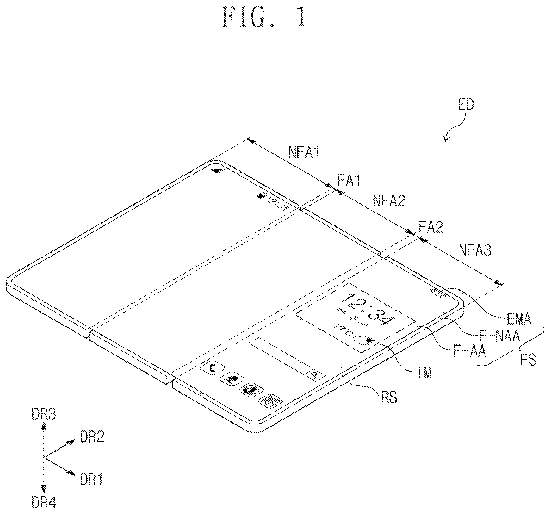
illustrates an assembled perspective view showing an electronic apparatus according to one or more embodiments. A illustrates a perspective view showing a folded electronic device according to one or more embodiments. B illustrates a perspective view showing a folded electronic device according to one or more embodiments.
An electronic device ED according to one or more embodiments may be an apparatus that is activated with an electrical signal. For example, the electronic device ED may be a mobile phone, a tablet computer, an automotive navigation system, a game console, or a wearable apparatus, but the present disclosure is not limited thereto. In this description, a mobile phone is illustrated by way of example as the electronic device ED.
The following figures including show first, second, third, and fourth directional axes DR 1 , DR 2 , DR 3 , and DR 4 , and in this description, directions indicated by the first to fourth directional axes DR 1 to DR 4 are relative concepts, and may thus be changed to other directions. In the following description, directions designated by the first, second, third, and fourth directional axes DR 1 , DR 2 , DR 3 , and DR 4 are respectively described as first, second, third, and fourth directions.
Referring to , the electronic device ED according to one or more embodiments may include a display surface FS parallel to a surface defined by the first direction DR 1 and the second direction DR 2 , which cross each other in an unfolded state of the electronic device ED. The electronic device ED may use the display surface FS to provide users with an image IM. The electronic device ED according to one or more embodiments may display the image IM in the third direction DR 3 on the display surface FS, which is parallel to each of the first direction DR 1 and the second direction DR 2 .
In this description, a front surface (or top surface) and a rear surface (bottom surface) of each of components are defined based on a direction along which the image IM is displayed. In this description, the direction along which the image IM is displayed may be the third direction DR 3 , and the fourth direction DR 4 may be defined to indicate a direction opposite to the third direction DR 3 .
The electronic device ED according to one or more embodiments may detect externally applied inputs. The external input may include various inputs provided from outside the electronic device ED. For example, the external input may not only include touch of a user's hand or other body part, but may include any input (e.g., hovering touch) that approaches or is in the vicinity of the electronic device ED. In addition, the external input may include force, pressure, light, or any of other external inputs.
The electronic device ED may include an active area F-AA and a peripheral area F-NAA. The active area F-AA may be a zone activated with an electric signal. The electronic device ED according to one or more embodiments may display the image IM through the active area F-AA. In addition, the active area F-AA may detect various types of external input. The peripheral area F-NAA is adjacent to the active area F-AA. The peripheral area F-NAA may have a corresponding color.
The active area F-AA may include an electronic module area EMA. Various electronic modules may be located on the electronic module area EMA. For example, the electronic module may include at least one selected from cameras, speakers, optical sensors, and/or thermal sensors. The electronic module area EMA may detect an external object received through the display surface FS, or may externally provide sound signals, such as voices, through the display surface FS. The electronic module may include a plurality of components, and is not limited.
The electronic module area EMA may be surrounded by the active area F-AA and/or the peripheral area F-NAA. The electronic module area EMA may be located in the active area F-AA, but the present disclosure is not limited. In addition, when inactivating the electronic modules located on the electronic module area EMA, the electronic module area EMA may not be visible to users, and a video or image may be displayed on the display surface FS.
The electronic device ED of one or more embodiments may have a rear surface RS opposite to the display surface FS. In one or more embodiments, the rear surface RS may be an outer surface of the electronic device ED, and no video or image may be displayed on the rear surface RS. The present disclosure, however, is not limited thereto, and the rear surface RS may also serve as a display surface on which a video or image is displayed. Moreover, the electronic device ED of one or more embodiments may further include an electronic module area located on the rear surface RS. The electronic module area located on the rear surface RS may include a camera, a speaker, an optical sensor, or the like.
In the electronic device ED of one or more embodiments, the peripheral area F-NAA may surround the active area F-AA. Therefore, a shape of the active area F-AA may be substantially defined by the peripheral area F-NAA. This, however, is illustrated by way of example, and the peripheral area F-NAA may be located adjacent to only one side of the active area F-AA, or may be omitted. The electronic device ED according to one or more embodiments may include the variously shaped active area F-AA, and the present disclosure is not limited.
The electronic device ED of one or more embodiments may include folding regions FA 1 and FA 2 and non-folding regions NFA 1 , NFA 2 , and NFA 3 . The electronic device ED may include a first non-folding region NFA 1 , a first folding region FA 1 , a second non-folding region NFA 2 , a second folding region FA 2 , and a third non-folding region NFA 3 that are arranged to be spaced apart from each other along the first direction DR 1 . The first non-folding region NFA 1 and the second non-folding region NFA 2 may be spaced apart from each other across the first folding region FA 1 . The second non-folding region NFA 2 and the third non-folding region NFA 3 may be spaced apart from each other across the second folding region FA 2 .
In one or more embodiments, the folding regions FA 1 and FA 2 may correspond to foldable components of the components included in the electronic device ED, and the non-folding regions NFA 1 , NFA 2 , and NFA 3 may correspond to flat ones of components included in the electronic device ED. Although depicts that two folding regions FA 1 and FA 2 are located between three non-folding regions NFA 1 , NFA 2 , and NFA 3 , the present disclosure is not limited thereto, and one of the folding regions FA 1 and FA 2 may be omitted or at least three folding regions may be provided.
Referring to A , in a folding mode of one or more embodiments, an electronic device ED-S 1 may include a first folding region FA 1 folded along a first folding axis FX 1 that extends along the second direction DR 2 , and may also include a second folding region FA 2 folded along a second folding axis FX 2 that extends along the second direction DR 2 and is spaced apart in the first direction DR 1 from the first folding axis FX 1 . The present disclosure, however, is not limited thereto, and the first folding axis FX 1 and the second folding axis FX 2 may be parallel to an arbitrary direction other than the second direction DR 2 .
In the presently described one or more embodiments, the first folding axis FX 1 may be defined on the active area F-AA that overlaps the first folding region FA 1 . Therefore, the first folding region FA 1 may be folded to allow the active area F-AA that overlaps the first non-folding region NFA 1 to face the active area F-AA that overlaps the second non-folding region NFA 2 .
In the presently described one or more embodiments, the second folding axis FX 2 may be defined on the rear surface RS that overlaps the second folding region FA 2 . Therefore, the second folding region FA 2 may be folded to allow the rear surface RS that overlaps the second non-folding region NFA 2 to face the rear surface RS that overlaps the third non-folding region NFA 3 .
According to the presently described one or more embodiments, an inner-folding (or in-folding) state may be defined to indicate a state in which a portion of the electronic device ED-S 1 is folded along the first folding axis FX 1 , and an outer-folding (or out-folding) state may be defined to indicate a state in which a portion of the electronic device ED-S 1 is folded along the second folding axis FX 2 . In a folding state, the first folding region FA 1 and the second folding region FA 2 may have their curvatures that are the same as each other, or different from each other, but the present disclosure is not limited.
Referring to B , in a folding mode of one or more embodiments, an electronic device ED-S 2 may include a first folding region FA 1 folded along a first folding axis FX 1 that extends along the second direction DR 2 , and may also include a second folding region FA 2 folded along a second folding axis FX 2 that extends along the second direction DR 2 , and that is spaced apart in the first direction DR 1 from the first folding axis FX 1 . The present disclosure, however, is not limited thereto, and the first folding axis FX 1 and the second folding axis FX 2 may be parallel to an arbitrary direction other than the second direction DR 2 .
In the presently described one or more embodiments, the first folding axis FX 1 may be defined on the active area F-AA that overlaps the first folding region FA 1 . Therefore, the first folding region FA 1 may be folded to allow the active area F-AA that overlaps the first non-folding region NFA 1 to face the active area F-AA that overlaps the second non-folding region NFA 2 .
In the presently described one or more embodiments, the second folding axis FX 2 may be defined on the active area F-AA that overlaps the second folding region FA 2 . Therefore, the second folding region FA 2 may be folded to allow the rear surface RS that overlaps the first non-folding region NFA 1 to face the active area F-AA that overlaps the third non-folding region NFA 3 .
According to the presently described one or more embodiments, an inner-folding state may be defined to indicate a state in which a portion of the electronic device ED-S 2 is folded along one or both of the first direction DR 1 and the second direction DR 2 . In a folding state, the first folding region FA 1 and the second folding region FA 2 may have their curvatures that are the same as each other, or different from each other, but the present disclosure is not limited.
A illustrates an exploded perspective view showing an electronic device according to one or more embodiments. B illustrates a cross-sectional view showing an electronic device according to one or more embodiments. C illustrates a cross-sectional view showing an electronic device according to one or more embodiments. D illustrates a cross-sectional view showing a folded plate according to one or more embodiments.
Referring to A and 3 B , the electronic device ED of one or more embodiments may include a window WM, an upper film FU, a display module DM, a lower film CPL, a plate PL, and a housing HAU. The electronic device ED may include adhesion layers AD 0 , AD 1 , AD 2 , AD 3 , AD 4 , and AD 5 that are located between respective components to couple adjacent components to each other.
The electronic device ED of one or more embodiments may further include a hinge member that guides a folding state. The hinge member may be located below the plate PL. A omits illustration of the electronic module area EMA and the electronic modules located below the electronic module area EMA discussed in .
The window WM may be located on the display module DM. The window WM may cover an entire top surface of the display module DM. The window WM may include an optically transparent dielectric material.
The window WM may include a thin glass substrate UT, a window protection layer PF located on the thin glass substrate UT, and a bezel pattern BZP. The window WM according to one or more embodiments may further include a functional layer HC located on the window protection layer PF.
The window protection layer PF and the thin glass substrate UT may be coupled to each other through an adhesion layer AD 0 . The adhesion layer AD 0 may include one of a pressure sensitive adhesive film (PSA) and an optically clear adhesive (OCA). In the following description, an adhesion layer may include one of a pressure sensitive adhesive film (PSA) and an optically clear adhesive (OCA), and a repetitive explanation will be omitted.
The window protection layer PF may be located on the thin glass substrate UT. The window protection layer PF may protect the thin glass substrate UT.
The window protection layer PF may include a synthetic resin film. The synthetic resin film of the window protection layer PF may include polyimide, polycarbonate, polyamide, triacetylcellulose, polymethylmethacrylate, or polyethylene terephthalate.
The functional layer HC may be located on the window protection layer PF. The functional layer HC may include at least one selected from a hard-coating layer, an anti-fingerprint layer, and/or an antireflective layer. When the functional layer HC includes a hard-coating layer, the functional layer HC may have a thickness ranging from about 3 μm to about 10 μm.
The thin glass substrate UT may be located below the window protection layer PF. The thin glass substrate UT may have a thickness ranging from about 25 μm to about 100 μm. The thin glass substrate UT may be a chemically strengthened glass. Even when the thin glass substrate UT repeats its folding and unfolding operations, the thin glass substrate UT may reduce, minimize, or prevent the occurrence of wrinkles.
The bezel pattern BZP may overlap the peripheral area F-NAA depicted in . The bezel pattern BZP may be located on a rear surface of the thin glass substrate UT. B depicts, by way of example, the bezel pattern BZP located on the rear surface of the thin glass substrate UT. The present disclosure is not limited thereto, and the bezel pattern BZP may be located between the window protection layer PF and the thin glass substrate UT. The bezel pattern BZP may be a colored light-shield layer formed by, for example, a coating method. The bezel pattern BZP may include a base material and a dye or pigment mixed in the base material.
The window WM and the upper film FU may be coupled to each other through a first adhesion layer AD 1 .
The upper film FU may be located between the window WM and the display module DM. The upper film FU may adsorb impact applied to a front surface of the electronic device ED. The upper film FU may include a synthetic resin film. The synthetic resin film may include polyimide, polycarbonate, polyamide, triacetyl cellulose, polymethylmethacrylate, or polyethylene terephthalate. In one or more embodiments, the upper film FU may be omitted.
The upper film FU and the display module DM may be coupled to each other through a second adhesion layer AD 2 .
The display module DM may be located below the window WM. The display module DM may be flexible. The display module DM may include a display area DP-DA and a non-display area DP-NDA that respectively correspond to the active area F-AA and the peripheral area F-NAA of the electronic device ED depicted in .
The display module DM may include a display panel that displays an image, and an input sensor that detects an external input. The display panel may be an emissive display panel, but the present disclosure is not particularly limited thereto. For example, the display panel may be an organic light-emitting display panel or a quantum-dot light-emitting display panel. An emission layer of the organic light-emitting display panel may include an organic light-emitting material. An emission layer of the inorganic light-emitting display panel may include a quantum-dot or a quantum-rod.
The display panel may include a plurality of emission elements. The emission elements may be located on the display area DP-DA, and may emit corresponding colors. When the emission layer is provided in plural, the emission elements may correspond to the emission layers. Alternatively, when the emission layer is provided as a single layer, the emission elements may respectively correspond to color filters or color conversion members.
The input sensor may be located on the display panel. The input sensor may operate in a capacitive manner. The input sensor may detect a position and/or strength of a user's hand over a front surface of the display area DP-DA. The input sensor may be formed on the display panel by a series of processes. In this case, it may be expressed that the input sensor is directly located on the display panel. The phrase “directly located” may mean that no component is located between the input sensor and the display panel. For example, no adhesive member may be separately located between the input sensor and the display panel.
The display module DM and the lower film CPL may be coupled to each other through a third adhesion layer AD 3 .
The lower film CPL may be located below the display module DM. The lower film CPL may have a corresponding color. The lower film CPL may reduce or prevent an optical transparency of a rear surface of the display module DM, while protecting the rear surface of the display module DM. The lower film CPL may be formed of a material whose light absorption is high. The lower film CPL may include a flexible synthetic resin film. For example, the lower film CPL may include polyethylene terephthalate.
The lower film CPL may be coupled to the plate PL through a fourth adhesion layer AD 4 . The fourth adhesion layer AD 4 according to the presently described one or more embodiments may include/define an opening OP 4 (which may be referred to as a first opening in the claims) that overlaps the first folding region FA 1 , and that partially exposes the plate PL and the lower film CPL.
The plate PL may be located below the display module DM to protect the display module DM against external impact. In one or more embodiments, the plate PL may include a metallic material or a polymeric material. For example, the plate PL may be formed of a stainless steel, aluminum, or any alloy thereof. According to one or more embodiments, the plate PL may include a fiber-reinforced composite material. The plate PL may include a reinforced fiber located in a matrix portion. The reinforced fiber may be a carbon fiber or a glass fiber. The matrix portion may include a polymer resin. The matrix portion may include a thermoplastic resin. For example, the matrix portion may include a polyamide-based resin or a polypropylene-based resin. For example, the fiber-reinforced composite material may include a carbon-fiber-reinforced plastic (CFRP) or a glass-fiber-reinforced plastic (GFRP).
The plate PL may include folding parts FS 1 and FS 2 and non-folding parts NFS 1 , NFS 2 , and NFS 3 . A first folding part FS 1 may overlap the first folding region FA 1 , and a second folding part FS 2 may overlap the second folding region FA 2 . A width in the first direction DR 1 of the first folding part FS 1 may be less than a width in the first direction DR 1 of the second folding part FS 2 .
The first folding part FS 1 may include a plurality of first holes MOP 1 . The first holes MOP 1 may be formed to penetrate in the third direction DR 3 through the first folding part FS 1 . The first folding part FS 1 except the first holes MOP 1 may have a slit shape/pattern in plan view.
The second folding part FS 2 may include a plurality of second holes MOP 2 . The second holes MOP 2 may be formed to penetrate in the third direction DR 3 through the second folding part FS 2 . The second folding part FS 2 except the second holes MOP 2 may have a slit shape/pattern in plan view.
A first non-folding part NFS 1 may overlap the first non-folding region NFA 1 , a second non-folding part NFS 2 may overlap the second non-folding region NFA 2 , and a third non-folding part NFS 3 may overlap the third non-folding region NFA 3 .
According to one or more embodiments, the opening OP 4 defined in the fourth adhesion layer AD 4 may at least partially overlap the first folding part FS 1 and only some of the first holes MOP 1 . Therefore, the first holes MOP 1 that overlap the opening OP 4 may be exposed from the fourth adhesion layer AD 4 through the opening OP 4 . For example, the opening OP 4 may extend from an area over one of the first holes MOP 1 nearest the first non-folding part NFS 1 to an area over one of the first holes MOP 1 that overlaps a center of, or a region near the center of, the first folding part FS 1 .
A fifth adhesion layer AD 5 may be located below the plate PL. The plate PL may be coupled through the fifth adhesion layer AD 5 to the hinge member that guides a folding operation. The fifth adhesion layer AD 5 according to one or more embodiments may include/define a first opening OP 5 - 1 (which may be referred to as a third opening in the claims), which overlaps the first folding part FS 1 , and may also include/define a second opening OP 5 - 2 (which may be referred to as a fourth opening in the claims), which overlaps the second folding part FS 2 .
According to the presently described one or more embodiments, as the fourth adhesion layer AD 4 and the fifth adhesion layer AD 5 respectively include/define the openings OP 4 , OP 5 - 1 , and OP 5 - 2 that overlap corresponding ones of the folding parts FS 1 and FS 2 , even when the folding parts FS 1 and FS 2 are repeatedly folded, it may be possible to reduce stress applied to the fourth adhesion layer AD 4 and the fifth adhesion layer AD 5 that overlap the folding parts FS 1 and FS 2 . Accordingly, the electronic device ED may have improved folding properties.
The electronic device ED according to one or more embodiments may further include a lower support member located below the plate PL. The lower support member may include at least one selected from a support layer, a cushion layer, a shield layer, and/or an interlayer bonding layer.
The housing HAU and the window WM may be coupled to each other to define an appearance of the electronic device ED. The housing HAU may provide a space capable of receiving the display module DM, the plate PL, the upper film FU, the lower film CPL, the hinge member, and the electronic module.
Referring to C , the electronic device ED- 1 according to one or more embodiments may include a window WM, an upper film FU, a display module DM, a lower film CPL, a plate PL- 1 , and a housing HAU. The electronic device ED- 1 may include adhesion layers AD 0 , AD 1 , AD 2 , AD 3 , AD 4 - 1 , and AD 5 that are located between respective components to couple adjacent components to each other. A description of the window WM, the upper film FU, the display module DM, the housing HAU, and the adhesion layers AD 0 , AD 1 , AD 2 , AD 3 , and AD 5 may correspond to that discussed in the electronic device ED of A .
The plate PL- 1 may include folding parts FS 1 and FS 2 and non-folding parts NFS 1 , NFS 2 , and NFS 3 . A first folding part FS 1 may overlap the first folding region FA 1 , and a second folding part FS 2 may overlap the second folding region FA 2 . In one or more embodiments, a width in the first direction DR 1 of the first folding part FS 1 may be less than a width in the first direction DR 1 of the second folding part FS 2 .
Referring to C and 3 D , the first folding part FS 1 according to one or more embodiments may include a first side curvature part SCM 1 , a first flat part NCM 1 , a main curvature part CM, a second flat part NCM 2 , and a second side curvature part SCM 2 . The first side curvature part SCM 1 may extend from the first non-folding part NFS 1 , and the second side curvature part SCM 2 may extend from the second non-folding part NFS 2 .
The main curvature part CM may be located between, and spaced apart from, the first side curvature part SCM 1 and the second side curvature part SCM 2 . The first flat part NCM 1 may be located between the first side curvature part SCM 1 and the main curvature part CM, and the second flat part NCM 2 may be located between the second side curvature part SCM 2 and the main curvature part CM.
The plate PL- 1 may include main holes MOP 1 (which may be referred to as first holes in the claims) that overlap the main curvature part CM, and that penetrate from top to bottom surfaces P-U and P-B of the plate PL- 1 .
The plate PL- 1 may include first side holes SOP 1 that overlap the first side curvature part SCM 1 , and that partially penetrate in a thickness direction of the plate PL- 1 from the bottom surface P-B of the plate PL- 1 .
In addition, the plate PL- 1 may include second side holes SOP 2 that overlap the second side curvature part SCM 2 , and that partially penetrate in the thickness direction of the plate PL- 1 from the bottom surface P-B of the plate PL- 1 .
When the electronic device ED- 1 is folded in a folding mode, the first side curvature part SCM 1 of the first folding part FS 1 may be folded with a first curvature radius R 1 along a first axis RX 1 to thereby have a first curvature. The main curvature part CM may be folded with a second curvature radius R 2 along a second axis RX 2 to thereby have a second curvature, and the second side curvature part SCM 2 may be folded with a third curvature radius R 3 along a third axis RX 3 to thereby have a third curvature. According to one or more embodiments, the first curvature and the third curvature may correspond to each other, and the first curvature may be less than the second curvature.
A center of curvature of the main curvature part CM may be defined on the top surface P-U of the plate PL- 1 . Therefore, a center of curvature of the main curvature part CM may be defined on a top surface of the window WM. A center of curvature of each of the first and second side curvature parts SCM 1 and SCM 2 may be defined on the bottom surface P-B of the plate PL- 1 . Therefore, the center of curvature of each of the first and second side curvature parts SCM 1 and SCM 2 may be defined on a bottom surface of the window WM.
According to one or more embodiments, as the first folding part FS 1 includes the holes MOP 1 , SOP 1 , and SOP 2 , which are included in the main curvature part CM, and also includes the first side curvature part SCM 1 and the second side curvature part SCM 2 , a shape of the first folding part FS 1 may be suitably changed in a folding mode.
In addition, as the main curvature part CM, the first side curvature part SCM 1 , and the second side curvature part SCM 2 are folded in different directions from each other, the first and second non-folding parts NFS 1 and NFS 2 of the plate PL- 1 may be located considerably adjacent to each other when the electronic device ED- 1 is in a folding mode, and thus the electronic device ED- 1 may be folded in an inner-folding manner to allow the first and second non-folding regions NFA 1 and NFA 2 of the plate PL- 1 to be relatively quite close to each other. Accordingly, the electronic device ED- 1 may become slimmer in a folding state.
illustrates a cross-sectional view showing a folded electronic device according to one or more embodiments. illustrates a cross-sectional view showing an electronic device according to one or more embodiments. The same or similar reference numerals are allocated to components that are the same as or similar to those discussed in to 3 D , and a repetitive description will be omitted.
depicts the window WM, the display module DM, and an adhesion layer AD located between the window WM and the display module DM among the components of A and 3 B , and other components will be omitted for convenience of description.
An electronic device ED-S 1 a according to the presently described one or more embodiments may be folded in the same manner as that of the electronic device ED-S 1 discussed in A .
Referring to , the electronic device ED-S 1 a according to one or more embodiments may be in-folded in a folding mode such that the first folding part (see FS 1 of A ) is folded in an inner-folding manner along the first folding axis FX 1 . Therefore, a top surface W-U of the window WM that overlaps the first non-folding region NFA 1 may face a top surface W-U of the window WM that overlaps the second non-folding region NFA 2 .
The electronic device ED-S 1 a may be out-folded in a folding mode such that the second folding part (see FS 2 of A ) is folded in an outer-folding manner along the second folding axis FX 2 . Therefore, a bottom surface W-B of the window WM that overlaps the second non-folding region NFA 2 may face a bottom surface W-B of the window WM that overlaps the third non-folding region NFA 3 . In this case, a curvature of the first folding part FS 1 may be greater than that of the second folding part FS 2 .
When the electronic device ED-S 1 a is folded, the adhesion layers AD may be placed between respective components to securely obtain decoupling characteristics between stacked components of the electronic device ED-S 1 a . Therefore, when the electronic device ED-S 1 a is in a folding operation, the window WM and the display module DM may be shifted some distance with respect to each other via the adhesion layer AD, and thus, an end of the window WM and an end of the display module DM may be spaced apart from each other in a folding state. An increase in thickness of the adhesion layer AD located between components may induce an improvement in decoupling characteristics. However, when the thickness of the adhesion AD is increased, a buckling phenomenon may occur at a location that overlaps the folding parts FS 1 and FS 2 . In one or more embodiments, the buckling phenomenon may occur at the window WM to which maximum or relatively high compressive stress is applied in a folding state. The term “bucking phenomenon BP,” which will be discussed in the following drawings, may be defined to indicate a location in the window WM to which maximum or relatively high compressive stress is applied in a folding state or an abnormal bending or distortion at the location in the window WM.
In a folding mode of the electronic device ED-S 1 a according to the presently described one or more embodiments, the window WM on the first folding region FA 1 may experience a buckling phenomenon BP at a corresponding point that is adjacent to the first non-folding region NFA 1 .
For example, when the electronic device ED-S 1 a is folded, a portion of the window WM that is adjacent to the second non-folding region NFA 2 , and that is on the first folding region FA 1 , may have an allowance space capable of being shifted a corresponding distance toward the second non-folding region NFA 2 , the second folding region FA 2 , and the third non-folding region NFA 3 . However, a portion of the window WM that is adjacent to the first non-folding region NFA 1 and that is on the first folding region FA 1 may have a relatively deficient allowance space capable of being shifted because an end of the first non-folding part NFS 1 is coupled through the adhesion layer AD to an end of the display module DM. Accordingly, in a folding mode of the electronic device ED-S 1 a according to the presently described one or more embodiments, a buckling phenomenon BP may occur at the window WM on the first folding region FA 1 at an area of the window WM that is adjacent to the first non-folding region NFA 1 .
An illustration of an electronic device ED-A that will be discussed with respect to may correspond to the cross section of the electronic device ED-S 1 a discussed in . Therefore, in a folding mode, the electronic device ED-A may be folded in the same operating state as that of the electronic device ED-S 1 discussed in A , and components included in the electronic device ED-A may correspond to those of included in the electronic device ED discussed in B .
In a folding mode, the electronic device ED-A may experience a buckling phenomenon BP at a corresponding point of the window WM that overlaps the first folding region FA 1 . For example, the window WM on the first folding region FA 1 may experience a buckling phenomenon BP at a corresponding point adjacent to the first non-folding region NFA 1 .
Referring to , the electronic device ED-A according to one or more embodiments may include a window WM, an upper film FU, a display module DM, a lower film CPL, a plate PL-A, and a housing (see HAU of A ). The electronic device ED-A may include adhesion layers AD 1 , AD 2 , AD 3 , AD 4 -A, and AD 5 that are located between respective components to couple adjacent components to each other. A description of the window WM, the upper film FU, the display module DM, the lower film CPL, the adhesion layers AD 1 , AD 2 , AD 3 , and AD 5 may correspond to that discussed in the electronic device ED of A .
The plate PL-A may include folding parts FS 1 and FS 2 and non-folding parts NFS 1 , NFS 2 , and NFS 3 . A first folding part FS 1 may overlap the first folding region FA 1 , and a second folding part FS 2 may overlap the second folding region FA 2 . A width in the first direction DR 1 of the first folding part FS 1 may be less than a width in the first direction DR 1 of the second folding part FS 2 .
The first folding part FS 1 may include a plurality of first holes MOP 1 . The first holes MOP 1 may be formed to penetrate in the third direction DR 3 through the first folding part FS 1 . The first folding part FS 1 except the first holes MOP 1 may have a slit shape/pattern in plan view.
The second folding part FS 2 may include a plurality of second holes MOP 2 . The second holes MOP 2 may be formed to penetrate in the third direction DR 3 through the second folding part FS 2 . The second folding part FS 2 except the second holes MOP 2 may have a slit shape/pattern in plan view.
A first non-folding part NFS 1 may overlap the first non-folding region NFA 1 , a second non-folding part NFS 2 may overlap the second non-folding region NFA 2 , and a third non-folding part NFS 3 may overlap the third non-folding region NFA 3 .
In one or more embodiments, the window WM on the first folding region FA 1 may experience a buckling phenomenon BP at a corresponding point adjacent to the first non-folding region NFA 1 .
The lower film CPL may be coupled to the plate PL through a fourth adhesion layer AD 4 -A. The fourth adhesion layer AD 4 -A may include/define an opening OP 4 (which may be referred to as a first opening in claims) that overlaps the first folding region FA 1 and that partially exposes the plate PL-A and the lower film CPL.
According to one or more embodiments, the opening OP 4 defined in the fourth adhesion layer AD 4 -A may overlap the first folding part FS 1 and only some of the first holes MOP 1 . Therefore, the first holes MOP 1 that overlap the opening OP 4 may be exposed from the fourth adhesion layer AD 4 -A through the opening OP 4 . For example, the opening OP 4 may extend from an area over one of the first holes MOP 1 nearest the first non-folding part NFS 1 to an area over one of the first holes MOP 1 that overlaps a center of, or a region near the center of, the first folding part FS 1 .
According to the presently described one or more embodiments, in a folding mode of the electronic device ED-A, the opening OP 4 defined in the fourth adhesion layer AD 4 -A may overlap a location at which a buckling phenomenon BP occurs. As the opening OP 4 is formed at a location to which maximum or relatively high compressive stress is applied when the first folding part FS 1 is folded in a folding mode, the compressive stress that is applied to the portion of the window WM that overlaps the opening OP 4 may be reduced. Therefore, it may be possible to reduce or prevent the occurrence of bucking issues, and to obtain the characteristics for reducing buckling. Accordingly, the electronic device ED-A may exhibit improved folding properties.
illustrates a cross-sectional view showing a folded electronic device according to one or more embodiments. illustrates a cross-sectional view showing an electronic device according to one or more embodiments. The same or similar reference numerals are allocated to components that are the same as or similar to those discussed in to 6 , and a repetitive description will be omitted.
depicts the window WM, the display module DM, and the adhesion layer AD located between the window WM and the display module DM among the components of A and 3 C , and other components will be omitted for convenience of description.
An electronic device ED-S 1 b according to the presently described one or more embodiments may be folded in the same manner as that of the electronic device ED-S 1 discussed in A .
Referring to , the electronic device ED-S 1 b according to one or more embodiments may be in-folded in a folding mode such that the first folding part (see FS 1 of A ) is folded in an inner-folding manner along the first folding axis FX 1 . Therefore, a top surface W-U of the window WM that overlaps the first non-folding region NFA 1 may face a top surface W-U of the window WM that overlaps the second non-folding region NFA 2 .
The electronic device ED-S 1 b may be out-folded in a folding mode such that the second folding part (see FS 2 of A ) is folded in an outer-folding manner along the second folding axis FX 2 . Therefore, a bottom surface W-B of the window WM that overlaps the second non-folding region NFA 2 may face a bottom surface W-B of the window WM that overlaps the third non-folding region NFA 3 . In this case, a curvature of the first folding part FS 1 may be the same as, or greater than, that of the second folding part FS 2 .
In a folding mode of the electronic device ED-S 1 b according to the presently described one or more embodiments, the window WM on the first folding region FA 1 may experience a buckling phenomenon BP at a corresponding point adjacent to the first non-folding region NFA 1 .
An illustration of an electronic device ED-B that will be discussed in may correspond to the cross section of the electronic device ED-S 1 b discussed in . Therefore, the electronic device ED-B may be folded in the same operating state as that of the electronic device ED-S 1 discussed in A .
Referring to , the electronic device ED-B according to one or more embodiments may include a window WM, an upper film FU, a display module DM, a lower film CPL, a plate PL-B, and a housing (see HAU of A ). The electronic device ED-B may include adhesion layers AD 1 , AD 2 , AD 3 , AD 4 -B, and AD 5 located between respective components to couple neighboring components to each other. A description of the window WM, the upper film FU, the display module DM, the lower film CPL, the adhesion layers AD 1 , AD 2 , AD 3 , and AD 5 may correspond to that discussed in the electronic device ED- 1 of C .
In a folding mode, the electronic device ED-B may experience a buckling phenomenon BP at a corresponding point of the window WM that overlaps the first folding region FA 1 . For example, the window WM on the first folding region FA 1 may experience a buckling phenomenon BP at a corresponding point adjacent to the first non-folding region NFA 1 .
The plate PL-B may include folding parts FS 1 and FS 2 and non-folding parts NFS 1 , NFS 2 , and NFS 3 . A first folding part FS 1 may overlap the first folding region FA 1 , and a second folding part FS 2 may overlap the second folding region FA 2 . In one or more embodiments, a width in the first direction DR 1 of the first folding part FS 1 may be less than a width in the first direction DR 1 of the second folding part FS 2 .
A first non-folding part NFS 1 may overlap the first non-folding region NFA 1 , a second non-folding part NFS 2 may overlap the second non-folding region NFA 2 , and a third non-folding part NFS 3 may overlap the third non-folding region NFA 3 .
The first folding part FS 1 according to one or more embodiments may include a first side curvature part SCM 1 , a first flat part NCM 1 , a main curvature part CM, a second flat part NCM 2 , and a second side curvature part SCM 2 . The first side curvature part SCM 1 may extend from the first non-folding part NFS 1 , and the second side curvature part SCM 2 may extend from the second non-folding part NFS 2 .
The main curvature part CM may be located between, and spaced apart from, the first side curvature part SCM 1 and the second side curvature part SCM 2 . The first flat part NCM 1 may be located between the first side curvature part SCM 1 and the main curvature part CM, and the second flat part NCM 2 may be located between the second side curvature part SCM 2 and the main curvature part CM.
In one or more embodiments, in a folding mode, the electronic device ED-B may experience a buckling phenomenon BP at a corresponding point of the window WM that overlaps at least one selected from the first side curvature part SCM 1 , the first flat part NCM 1 , and/or the main curvature part CM.
The plate PL-B may include main holes MOP 1 (which may be referred to as first holes in the claims) that overlap the main curvature part CM, and that penetrate from top to bottom surfaces of the plate PL-B.
The plate PL-B may include first side holes SOP 1 that overlap the first side curvature part SCM 1 , and that partially penetrate in a thickness direction of the plate PL-B from the bottom surface of the plate PL-B.
In addition, the plate PL-B may include second side holes SOP 2 that overlap the second side curvature part SCM 2 , and that partially penetrate in the thickness direction of the plate PL-B from the bottom surface of the plate PL-B.
In the presently described one or more embodiments, a folding manner of the first folding part FS 1 of the electronic device ED-B may correspond to that of the first folding part FS 1 of the plate PL- 1 discussed in D .
The lower film CPL may be coupled to the plate PL-B through a fourth adhesion layer AD 4 -B. The fourth adhesion layer AD 4 -B may include/define an opening OP 4 (which may be referred to as a first opening in the claims) that overlaps the first folding region FA 1 and that partially exposes the plate PL-B and the lower film CPL.
According to one or more embodiments, the opening OP 4 defined in the fourth adhesion layer AD 4 -B may extend from an area over one of the first side holes SOP 1 nearest the first non-folding part NFS 1 to an area over one of the main holes MOP 1 that overlaps a center of, or a region near the center of, the main curvature part CM.
The present disclosure, however, is not limited thereto. The opening OP 4 defined in the fourth adhesion layer AD 4 -B may extend from the first flat part NCM 1 near the first side curvature part SCM 1 to an area over one of the main holes MOP 1 that overlaps a center of, or a region near the center of, the main curvature part CM, or may extend from an area over one of the main holes MOP 1 nearest the first flat part NCM 1 to an area over one of the main holes MOP 1 that overlaps a center of, or a region near the center of, the main curvature part CM, but the present disclosure is not limited.
According to the presently described one or more embodiments, in a folding mode of the electronic device ED-B, the opening OP 4 defined in the fourth adhesion layer AD 4 -B may overlap a location at which a buckling phenomenon BP occurs. Therefore, it may be possible to reduce or prevent the occurrence of bucking issues at a corresponding point of the window WM in a folding mode and to obtain the characteristics for reducing buckling. Accordingly, the electronic device ED-B may exhibit improved folding properties.
illustrates a cross-sectional view showing a folded electronic device according to one or more embodiments. illustrates a cross-sectional view showing an electronic device according to one or more embodiments. The same or similar reference numerals are allocated to components that are the same as or similar to those discussed in to 3 D , and a repetitive description will be omitted.
depicts the window WM, the display module DM, and the adhesion layer AD located between the window WM and the display module DM among the components of A and 3 B , and other components will be omitted for convenience of description.
An electronic device ED-S 2 a according to the presently described one or more embodiments may be folded in the same manner as that of the electronic device ED-S 2 discussed in B .
Referring to , the electronic device ED-S 2 a according to one or more embodiments may be in-folded in a folding mode such that the first folding part (see FS 1 of A ) is folded in an inner-folding manner along the first folding axis FX 1 . Therefore, a top surface W-U of the window WM that overlaps the first non-folding region NFA 1 may face a top surface W-U of the window WM that overlaps the second non-folding region NFA 2 .
The electronic device ED-S 2 a may be in-folded in a folding mode such that the second folding part (see FS 2 of A ) is folded in an inner-folding manner along the second folding axis FX 2 . Therefore, a bottom surface W-B of the window WM that overlaps the first non-folding region NFA 1 may face a top surface W-U of the window WM that overlaps the third non-folding region NFA 3 . In this case, a curvature of the first folding part FS 1 may be greater than that of the second folding part FS 2 .
In a folding mode of the electronic device ED-S 2 a according to the presently described one or more embodiments, the window WM on the first folding region FA 1 may experience a buckling phenomenon BP at a corresponding point adjacent to the second non-folding region NFA 2 .
An electronic device ED-C that will be discussed in may correspond to the cross section of the electronic device ED-S 2 a discussed in . Therefore, the electronic device ED-C may be folded in the same operating state as that of the electronic device ED-S 2 discussed in A .
Referring to , the electronic device ED-C according to one or more embodiments may include a window WM, an upper film FU, a display module DM, a lower film CPL, a plate PL-C, and a housing (see HAU of A ). The electronic device ED-C may include adhesion layers AD 1 , AD 2 , AD 3 , AD 4 -C, and AD 5 that are located between respective components to couple adjacent components to each other. A description of the window WM, the upper film FU, the display module DM, the lower film CPL, the adhesion layers AD 1 , AD 2 , AD 3 , and AD 5 may correspond to that discussed in the electronic device ED- 1 of C .
In a folding mode, the electronic device ED-C may experience a buckling phenomenon BP at a corresponding point of the window WM that overlaps the first folding region FA 1 . For example, the window WM on the first folding region FA 1 may experience a buckling phenomenon BP at a corresponding point adjacent to the second non-folding region NFA 2 .
The plate PL-C may include folding parts FS 1 and FS 2 and non-folding parts NFS 1 , NFS 2 , and NFS 3 . A first folding part FS 1 may overlap the first folding region FA 1 , and a second folding part FS 2 may overlap the second folding region FA 2 . A width in the first direction DR 1 of the first folding part FS 1 may be less than a width in the first direction DR 1 of the second folding part FS 2 .
The first folding part FS 1 may include a plurality of first holes MOP 1 . The first holes MOP 1 may be formed to penetrate in the third direction DR 3 through the first folding part FS 1 . The first folding part FS 1 except the first holes MOP 1 may have a slit shape/pattern in plan view.
The second folding part FS 2 may include a plurality of second holes MOP 2 . The second holes MOP 2 may be formed to penetrate in the third direction DR 3 through the second folding part FS 2 . The second folding part FS 2 except the second holes MOP 2 may have a slit shape/pattern in plan view.
A first non-folding part NFS 1 may overlap the first non-folding region NFA 1 , a second non-folding part NFS 2 may overlap the second non-folding region NFA 2 , and a third non-folding part NFS 3 may overlap the third non-folding region NFA 3 .
In the electronic device ED-C of one or more embodiments, the window WM on the first folding region FA 1 may experience a buckling phenomenon BP at a corresponding point adjacent to the second non-folding region NFA 2 .
The lower film CPL may be coupled to the plate PL-C through a fourth adhesion layer AD 4 -C. The fourth adhesion layer AD 4 -C according to the presently described one or more embodiments may include/define an opening OP 4 (which may be referred to as a first opening in the claims) that overlaps the first folding region FA 1 and that partially exposes the plate PL-C and the lower film CPL.
According to one or more embodiments, the opening OP 4 defined in the fourth adhesion layer AD 4 -C may overlap the first folding part FS 1 and only some of the first holes MOP 1 . Therefore, the first holes MOP 1 that overlap the opening OP 4 may be exposed from the fourth adhesion layer AD 4 -C through the opening OP 4 . For example, the opening OP 4 may extend from an area over one of the first holes MOP 1 nearest the second non-folding part NFS 2 to an area over one of the first holes MOP 1 that overlaps a center of, or a region near the center of, the first folding part FS 1 .
According to the presently described one or more embodiments, in a folding mode of the electronic device ED-C, the opening OP 4 defined in the fourth adhesion layer AD 4 -C may overlap a location at which a buckling phenomenon BP occurs. Therefore, it may be possible to reduce or prevent the occurrence of bucking issues at a corresponding point of the window WM in a folding mode and to obtain the characteristics for reducing buckling. Accordingly, the electronic device ED-C may exhibit improved folding properties.
illustrates a cross-sectional view showing a folded electronic device according to one or more embodiments. A illustrates a cross-sectional view showing an electronic device according to one or more embodiments. B illustrates a cross-sectional view showing an electronic device according to one or more embodiments. C illustrates a cross-sectional view showing an electronic device according to one or more embodiments. D illustrates a cross-sectional view showing an electronic device according to one or more embodiments. illustrates a graph showing stress on a folded portion of a window according to one or more embodiments. The same or similar reference numerals are allocated to components the same as or similar to those discussed in to 9 , and a repetitive description will be omitted.
depicts the window WM, the display module DM, and the adhesion layer AD located between the window WM and the display module DM among the components of A and 3 C , and other components will be omitted for convenience of description.
An electronic device ED-S 2 b according to the presently described one or more embodiments may be folded in the same manner as that of the electronic device ED-S 2 discussed in B .
Referring to , the electronic device ED-S 2 b according to one or more embodiments may be in-folded in a folding mode such that the first folding part (see FS 1 of A ) is folded in an inner-folding manner along the first folding axis FX 1 . Therefore, a top surface W-U of the window WM that overlaps the first non-folding region NFA 1 may face a top surface W-U of the window WM that overlaps the second non-folding region NFA 2 .
The electronic device ED-S 2 b may be in-folded in a folding mode such that the second folding part (see FS 2 of A ) is folded in an inner-folding manner along the second folding axis FX 2 . Therefore, a bottom surface W-B of the window WM that overlaps the first non-folding region NFA 1 may face a top surface W-U of the window WM that overlaps the third non-folding region NFA 3 . In this case, a curvature of the first folding part FS 1 may be greater than that of the second folding part FS 2 .
In a folding mode of the electronic device ED-S 2 b according to the presently described one or more embodiments, the window WM on the first folding region FA 1 may experience a buckling phenomenon BP at a corresponding point adjacent to the second non-folding region NFA 2 .
Each of electronic devices ED-D, ED-E, ED-F, and ED-G that will be discussed in A, 11 B, 11 C, and 11 C may correspond to the cross section of the electronic device ED-S 2 b discussed in . Therefore, the electronic devices ED-D, ED-E, ED-F, and ED-G may be folded in the same operating state as that of the electronic device ED-S 2 discussed in B .
Referring to A , the electronic device ED-D according to one or more embodiments may include a window WM, an upper film FU, a display module DM, a lower film CPL, a plate PL-D, and a housing (see HAU of A ). The electronic device ED-D may include adhesion layers AD 1 , AD 2 , AD 3 , AD 4 -D, and AD 5 that are located between respective components to couple adjacent components to each other. A description of the window WM, the upper film FU, the display module DM, the lower film CPL, the adhesion layers AD 1 , AD 2 , AD 3 , and AD 5 may correspond to that discussed in the electronic device ED- 1 of C .
In a folding mode, the electronic device ED-D may experience a buckling phenomenon BP at a corresponding point of the window WM that overlaps the first folding region FA 1 . For example, the window WM on the first folding region FA 1 may experience a buckling phenomenon BP at a corresponding point adjacent to the second non-folding region NFA 2 .
The plate PL-D may include folding parts FS 1 and FS 2 and non-folding parts NFS 1 , NFS 2 , and NFS 3 . A first folding part FS 1 may overlap the first folding region FA 1 , and a second folding part FS 2 may overlap the second folding region FA 2 . In one or more embodiments, a width in the first direction DR 1 of the first folding part FS 1 may be less than a width in the first direction DR 1 of the second folding part FS 2 .
A first non-folding part NFS 1 may overlap the first non-folding region NFA 1 , a second non-folding part NFS 2 may overlap the second non-folding region NFA 2 , and a third non-folding part NFS 3 may overlap the third non-folding region NFA 3 .
The first folding part FS 1 according to one or more embodiments may include a first side curvature part SCM 1 , a first flat part NCM 1 , a main curvature part CM, a second flat part NCM 2 , and a second side curvature part SCM 2 . The first side curvature part SCM 1 may extend from the first non-folding part NFS 1 , and the second side curvature part SCM 2 may extend from the second non-folding part NFS 2 .
The main curvature part CM may be located between and spaced apart from the first side curvature part SCM 1 and the second side curvature part SCM 2 . The first flat part NCM 1 may be located between the first side curvature part SCM 1 and the main curvature part CM, and the second flat part NCM 2 may be located between the second side curvature part SCM 2 and the main curvature part CM.
In one or more embodiments, in a folding mode, the electronic device ED-D may experience a buckling phenomenon BP at a corresponding point of the window WM that overlaps at least one selected from the second side curvature part SCM 2 , the second flat part NCM 2 , and/or the main curvature part CM.
The plate PL-D may include main holes MOP 1 (which may be referred to as first holes in the claims) that overlap the main curvature part CM, and that penetrate from top to bottom surfaces of the plate PL-D.
The plate PL-D may include first side holes SOP 1 that overlap the first side curvature part SCM 1 , and that partially penetrate in a thickness direction of the plate PL-D from the bottom surface of the plate PL-D.
In addition, the plate PL-D may include second side holes SOP 2 that overlap the second side curvature part SCM 2 , and that partially penetrate in the thickness direction of the plate PL-D from the bottom surface of the plate PL-D.
In the presently described one or more embodiments, a folding manner of the first folding part FS 1 of the electronic device ED-D may correspond to that of the first folding part FS 1 of the plate PL- 1 discussed in D .
The lower film CPL may be coupled to the plate PL-D through a fourth adhesion layer AD 4 -D. The fourth adhesion layer AD 4 -D according to the presently described one or more embodiments may include/define an opening OP 4 (which may be referred to as a first opening in the claims) that overlaps the first folding region FA 1 and that partially exposes the plate PL-D and the lower film CPL.
According to one or more embodiments, the opening OP 4 defined in the fourth adhesion layer AD 4 -D may extend from an area over one of the second side holes SOP 2 nearest the second non-folding part NFS 2 to an area over one of the main holes MOP 1 that overlaps a center of, or a region near the center of, the main curvature part CM.
According to the presently described one or more embodiments, in a folding mode of the electronic device ED-D, the opening OP 4 defined in the fourth adhesion layer AD 4 -D may overlap a location at which a buckling phenomenon BP occurs. Therefore, it may be possible to reduce or prevent the occurrence of bucking issues at a corresponding point of the window WM in a folding mode and to obtain the characteristics for reducing buckling. Accordingly, the electronic device ED-D may exhibit improved folding properties.
Referring to B , the electronic device ED-E according to one or more embodiments may include a window WM, an upper film FU, a display module DM, a lower film CPL, a plate PL-E, and a housing (see HAU of A ). The electronic device ED-E may include adhesion layers AD 1 , AD 2 , AD 3 , AD 4 -E, and AD 5 that are located between respective components to couple adjacent components to each other. A description of the window WM, the upper film FU, the display module DM, the lower film CPL, the adhesion layers AD 1 , AD 2 , AD 3 , and AD 5 may correspond to that discussed in the electronic device ED- 1 of C . In addition, a description of the plate PL-E included in the electronic device ED-E may correspond to that of the plate PL-D discussed in A .
The lower film CPL may be coupled to the plate PL-E through a fourth adhesion layer AD 4 -E. The fourth adhesion layer AD 4 -E according to the presently described one or more embodiments may include/define an opening OP 4 (also referred to as a first opening in the claims) that overlaps the first folding region FA 1 and that partially exposes the plate PL-E and the lower film CPL.
According to one or more embodiments, the opening OP 4 defined in the fourth adhesion layer AD 4 -E may extend from the second flat part NCM 2 near the second side curvature part SCM 2 to an area over one of the main holes MOP 1 that overlaps a center of, or a region near the center of, the main curvature part CM.
According to the presently described one or more embodiments, in a folding mode of the electronic device ED-E, the opening OP 4 defined in the fourth adhesion layer AD 4 -E may overlap a location at which a buckling phenomenon BP occurs. Therefore, it may be possible to reduce or prevent the occurrence of bucking issues at a corresponding point of the window WM in a folding mode and to obtain the characteristics for reducing buckling. Accordingly, the electronic device ED-E may exhibit improved folding properties.
Referring to C , the electronic device ED-F according to one or more embodiments may include a window WM, an upper film FU, a display module DM, a lower film CPL, a plate PL-F, and a housing (see HAU of A ). The electronic device ED-F may include adhesion layers AD 1 , AD 2 , AD 3 , AD 4 -F, and AD 5 that are located between respective components to couple adjacent components to each other. A description of the window WM, the upper film FU, the display module DM, the lower film CPL, the adhesion layers AD 1 , AD 2 , AD 3 , and AD 5 may correspond to that discussed in the electronic device ED- 1 of C . In addition, a description of the plate PL-F included in the electronic device ED-F may correspond to that of the plate PL-D discussed in A .
The lower film CPL may be coupled to the plate PL-F through a fourth adhesion layer AD 4 -F. The fourth adhesion layer AD 4 -F according to the presently described one or more embodiments may include/define an opening OP 4 (also referred to as a first opening in the claims) that overlaps the first folding region FA 1 and that partially exposes the plate PL-F and the lower film CPL.
According to one or more embodiments, the opening OP 4 defined in the fourth adhesion layer AD 4 -F may extend from an area over one of the main holes MOP 1 nearest the second non-folding part NFS 2 to an area over one of the main holes MOP 1 that overlaps a center of, or a region near the center of, the main curvature part CM.
According to the presently described one or more embodiments, in a folding mode of the electronic device ED-F, the opening OP 4 defined in the fourth adhesion layer AD 4 -F may overlap a location at which a buckling phenomenon BP occurs. Therefore, it may be possible to reduce or prevent the occurrence of bucking issues at a corresponding point of the window WM in a folding mode and to obtain the characteristics for reducing buckling. Accordingly, the electronic device ED-F may exhibit improved folding properties.
Referring to D , the electronic device ED-G according to one or more embodiments may include a window WM, an upper film FU, a display module DM, a lower film CPL, a plate PL-G, and a housing (see HAU of A ). The electronic device ED-G may include adhesion layers AD 1 , AD 2 , AD 3 , AD 4 -G, and AD 5 that are located between respective components to couple adjacent components to each other. A description of the window WM, the upper film FU, the display module DM, the lower film CPL, the adhesion layers AD 1 , AD 2 , AD 3 , and AD 5 may correspond to that discussed in the electronic device ED- 1 of C . In addition, a description of the plate PL-G included in the electronic device ED-G may correspond to that of the plate PL-D discussed in A .
The lower film CPL may be coupled to the plate PL-G through a fourth adhesion layer AD 4 -G. The fourth adhesion layer AD 4 -G according to the presently described one or more embodiments may include a first opening OP 4 - 1 that overlaps the first folding region FA 1 and that partially exposes the plate PL-G and the lower film CPL.
The fourth adhesion layer AD 4 -G according to one or more embodiments may include a second opening OP 4 - 2 that overlaps the second folding region FA 2 and that partially exposes the plate PL-G and the lower film CPL.
According to one or more embodiments, the first opening OP 4 - 1 defined in the fourth adhesion layer AD 4 -G may extend from an area over one of the second side holes SOP 2 nearest the second non-folding part NFS 2 to an area over one of the first holes MOP 1 that overlaps a center of, or a region near the center of, the main curvature part CM. The second opening OP 4 - 2 may extend from an area over one of the second holes MOP 2 nearest the second non-folding part NFS 2 to an area over one of the second holes MOP 2 that overlaps a center of, or a region near the center of, the second folding part FS 2 .
According to the presently described one or more embodiments, in a folding mode of the electronic device ED-G, the first opening OP 4 - 1 defined in the fourth adhesion layer AD 4 -G may overlap a location at which a buckling phenomenon BP occurs. In addition, as the second opening OP 4 - 2 is additionally located on the second folding part FS 2 , it may be possible to reduce compressive stress applied to the window WM that overlaps the second folding part FS 2 . Accordingly, the electronic device ED-G may exhibit improved folding properties.
illustrates a graph showing how stress changes with distance, the stress being applied to a corresponding point of the window WM that overlaps the first folding region FA 1 when the first folding part FS 1 is folded in an inner-folding manner along the first folding axis FX 1 , and when the second folding part FS 2 is folded in an outer-folding manner along the second folding axis FX 2 , as discussed in the electronic device ED-S 2 b of .
A first graph S 1 is a variation in stress applied to the window WM when the opening OP 4 is included in the electronic device ED-D, ED-E, ED-F, or ED-G, and a second graph S 2 is a variation in stress applied to the window WM when an opening is not included in any adhesion layer located between the window WM and the display module DM.
The symbol “CP” is shown to denote a corresponding point where maximum or relatively high tensile stress is applied to a window in a folding state. For example, as shown in , maximum or relatively high tensile stress (positive value) occurs at the corresponding point CP of the window WM, and maximum or relatively high compressive stress (negative value) occurs at a corresponding point of the window WM.
The second graph S 2 shows that the window WM experiences a buckling phenomenon BP when there is no reduction in stress applied to at the corresponding point of the window WM to which the maximum or relatively high compressive stress is applied. Alternatively, as the electronic devices ED-D, ED-E, ED-F, and ED-G according to one or more embodiments respectively include the adhesive layers AD 4 -D, AD 4 -E, AD 4 -G, and AD 4 -G, each of which being located between the window WM and the display module DM, it may be possible to reduce stress applied to the window WM, and accordingly to reduce or prevent the likelihood of the window WM undergoing a buckling phenomenon BP.
A illustrates a cross-sectional view showing an electronic device according to one or more embodiments. B illustrates a cross-sectional view showing an electronic device according to one or more embodiments. C illustrates a cross-sectional view showing an electronic device according to one or more embodiments. The same or similar reference numerals are allocated to components the same as or similar to those discussed in to 12 D , and a repetitive description will be omitted.
An illustration of each of electronic devices ED-H, ED-I, and ED-J which will be discussed in A, 13 B, and 13 C may correspond to the cross section of the electronic device ED-S 2 b discussed in . Therefore, the electronic devices ED-H, ED-I, and ED-J may be folded in the same operating state as that of the electronic device ED-S 2 discussed in B .
Referring to A , the electronic device ED-H according to one or more embodiments may include a window WM, an upper film FU, a display module DM, a lower film CPL, a plate PL-H, and a housing (see HAU of A ). The electronic device ED-H may include adhesion layers AD 1 , AD 2 , AD 3 -H, AD 4 , and AD 5 that are located between respective components to couple adjacent components to each other. A description of the window WM, the upper film FU, the display module DM, the lower film CPL, the adhesion layers AD 1 , AD 2 , AD 4 , and AD 5 may correspond to that discussed in the electronic device ED- 1 of C .
In a folding mode, the electronic device ED-H according to the present may experience a buckling phenomenon BP at a corresponding point of the window WM that overlaps the first folding region FA 1 . For example, the window WM on the first folding region FA 1 may experience a buckling phenomenon BP at a corresponding point adjacent to the second non-folding region NFA 2 .
The display module DM and the lower film CPL may be coupled to each other through a third adhesion layer AD 3 -H. The third adhesion layer AD 3 -H according to the presently described one or more embodiments may include/define an opening OP 3 that overlaps the first folding region FA 1 , and that partially exposes the display module DM and the lower film CPL.
The plate PL-H may include folding parts FS 1 and FS 2 and non-folding parts NFS 1 , NFS 2 , and NFS 3 . A first folding part FS 1 may overlap the first folding region FA 1 , and a second folding part FS 2 may overlap the second folding region FA 2 .
A first non-folding part NFS 1 may overlap the first non-folding region NFA 1 , a second non-folding part NFS 2 may overlap the second non-folding region NFA 2 , and a third non-folding part NFS 3 may overlap the third non-folding region NFA 3 .
The first folding part FS 1 according to one or more embodiments may include a first side curvature part SCM 1 , a first flat part NCM 1 , a main curvature part CM, a second flat part NCM 2 , and a second side curvature part SCM 2 . The first side curvature part SCM 1 may extend from the first non-folding part NFS 1 , and the second side curvature part SCM 2 may extend from the second non-folding part NFS 2 .
The plate PL-H may include main holes MOP 1 (which may be referred to as first holes in the claims) that overlap the main curvature part CM, and that penetrate from top to bottom surfaces of the plate PL-H.
The plate PL-H may include first side holes SOP 1 that overlap the first side curvature part SCM 1 , and that partially penetrate in a thickness direction of the plate PL-H from the bottom surface of the plate PL-H.
In addition, the plate PL-H may include second side holes SOP 2 that overlap the second side curvature part SCM 2 , and that partially penetrate in the thickness direction of the plate PL-H from the bottom surface of the plate PL-H.
According to one or more embodiments, the opening OP 3 defined in the third adhesion layer AD 3 -H may extend from an area over one of the second side holes SOP 2 nearest the second non-folding part NFS 2 to an area over one of the main holes MOP 1 that overlaps a center of, or a region near the center of, the main curvature part CM.
Referring to B , the electronic device ED-I according to one or more embodiments may include a window WM, an upper film FU, a display module DM, a lower film CPL, a plate PL-I, and a housing (see HAU of A ). The electronic device ED-I may include adhesion layers AD 1 , AD 2 -I, AD 3 , AD 4 , and AD 5 that are located between respective components to couple adjacent components to each other. A description of the window WM, the upper film FU, the display module DM, the lower film CPL, the adhesion layers AD 1 , AD 3 , AD 4 , and AD 5 may correspond to that discussed in the electronic device ED- 1 of C .
In a folding mode, the electronic device ED-I according to the present may experience a buckling phenomenon BP at a corresponding point of the window WM that overlaps the first folding region FA 1 . For example, the window WM on the first folding region FA 1 may experience a buckling phenomenon BP at a corresponding point adjacent to the second non-folding region NFA 2 .
The upper film FU and the display module DM may be coupled to each other through a second adhesion layer AD 2 -I. The second adhesion layer AD 2 -I according to the presently described one or more embodiments may include/define an opening OP 2 that overlaps the first folding region FA 1 and that partially exposes the upper film FU and the display module DM.
The plate PL-I may include folding parts FS 1 and FS 2 and non-folding parts NFS 1 , NFS 2 , and NFS 3 . A first folding part FS 1 may overlap the first folding region FA 1 , and a second folding part FS 2 may overlap the second folding region FA 2 .
A first non-folding part NFS 1 may overlap the first non-folding region NFA 1 , a second non-folding part NFS 2 may overlap the second non-folding region NFA 2 , and a third non-folding part NFS 3 may overlap the third non-folding region NFA 3 .
The first folding part FS 1 according to one or more embodiments may include a first side curvature part SCM 1 , a first flat part NCM 1 , a main curvature part CM, a second flat part NCM 2 , and a second side curvature part SCM 2 . The first side curvature part SCM 1 may extend from the first non-folding part NFS 1 , and the second side curvature part SCM 2 may extend from the second non-folding part NFS 2 .
The plate PL-I may include main holes MOP 1 (which may be referred to as first holes in the claims) that overlap the main curvature part CM, and that penetrate from top to bottom surfaces of the plate PL-I.
The plate PL-I may include first side holes SOP 1 that overlap the first side curvature part SCM 1 , and that partially penetrate in a thickness direction of the plate PL-I from the bottom surface of the plate PL-I.
In addition, the plate PL-I may include second side holes SOP 2 that overlap the second side curvature part SCM 2 , and that partially penetrate in the thickness direction of the plate PL-I from the bottom surface of the plate PL-I.
According to one or more embodiments, the opening OP 2 defined in the second adhesion layer AD 2 -I may extend from an area over one of the second side holes SOP 2 nearest the second non-folding part NFS 2 to an area over one of the main holes MOP 1 that overlaps a center of, or a region near the center of, the main curvature part CM.
Referring to C , the electronic device ED-J according to one or more embodiments may include a window WM, an upper film FU, a display module DM, a lower film CPL, a plate PL-J, and a housing (see HAU of A ). The electronic device ED-J may include adhesion layers AD 1 , AD 2 , AD 3 -J, AD 4 -J, and AD 5 that are located between respective components to couple adjacent components to each other. A description of the window WM, the upper film FU, the display module DM, the lower film CPL, the adhesion layers AD 1 , AD 2 , and AD 5 may correspond to that discussed in the electronic device ED- 1 of C .
In a folding mode, the electronic device ED-J according to the present may experience a buckling phenomenon BP at a corresponding point of the window WM that overlaps the first folding region FA 1 . For example, the window WM on the first folding region FA 1 may experience a buckling phenomenon BP at a corresponding point adjacent to the second non-folding region NFA 2 .
The display module DM and the lower film CPL may be coupled to each other through a third adhesion layer AD 3 -J, and the lower film CPL and the plate PL-J may be coupled to each other through a fourth adhesion layer AD 4 -J.
In the presently described one or more embodiments, the fourth adhesion layer AD 4 -J may include a first opening OP 4 that overlaps the first folding region FA 1 and that partially exposes the lower film CPL and the plate PL-J.
In addition, the third adhesion layer AD 3 -J may include a second opening OP 3 that overlaps the first folding region FA 1 and that partially exposes the display module DM and the lower film CPL.
The plate PL-J may include folding parts FS 1 and FS 2 and non-folding parts NFS 1 , NFS 2 , and NFS 3 . A first folding part FS 1 may overlap the first folding region FA 1 , and a second folding part FS 2 may overlap the second folding region FA 2 .
A first non-folding part NFS 1 may overlap the first non-folding region NFA 1 , a second non-folding part NFS 2 may overlap the second non-folding region NFA 2 , and a third non-folding part NFS 3 may overlap the third non-folding region NFA 3 .
The first folding part FS 1 according to one or more embodiments may include a first side curvature part SCM 1 , a first flat part NCM 1 , a main curvature part CM, a second flat part NCM 2 , and a second side curvature part SCM 2 . The first side curvature part SCM 1 may extend from the first non-folding part NFS 1 , and the second side curvature part SCM 2 may extend from the second non-folding part NFS 2 .
The plate PL-J may include main holes MOP 1 (which may be referred to as first holes in the claims) that overlap the main curvature part CM, and that penetrate from top to bottom surfaces of the plate PL-J.
The plate PL-J may include first side holes SOP 1 that overlap the first side curvature part SCM 1 , and that partially penetrate in a thickness direction of the plate PL-J from the bottom surface of the plate PL-J.
In addition, the plate PL-J may include second side holes SOP 2 that overlap the second side curvature part SCM 2 , and that partially penetrate in the thickness direction of the plate PL-J from the bottom surface of the plate PL-J.
According to one or more embodiments, the first opening OP 4 defined in the fourth adhesion layer AD 4 -J and the second opening OP 3 defined in the third adhesion layer AD 3 -J may extend from an area over one of the second side holes SOP 2 nearest the second non-folding part NFS 2 to an area over one of the main holes MOP 1 that overlaps a center of, or a region near the center of, the main curvature part CM.
According to the presently described one or more embodiments, as an opening of an adhesion layer is formed at a point of a window to which maximum or relatively high compressive stress is applied in a folding mode of an electronic device, it may be possible to reduce compressive stress applied to the window that overlaps the opening. Therefore, the occurrence of bucking issue may be reduced or prevented, while decoupling characteristics may be achieved, and as a result, it may be possible to provide an electronic device with improved folding properties.
Although the embodiments have been described with reference to a number of illustrative examples thereof, it will be understood by those of ordinary skill in the art that various changes in form and details may be made without departing from the spirit and scope of the present disclosure as set forth in the following claims. Thus, the technical scope of the present disclosure is not limited by the embodiments and examples described above, but by the following claims, with functional equivalents thereof to be included therein.
Figures (20)
Citations
This patent cites (13)
- US9874772
- US2018/0217639
- US2019/0334114
- US2020/0333522
- US2021/0068276
- US2021/0134192
- US2021/0174711
- US2022/0147107
- US2022/0199922
- US2022/0201879
- US110189638
- US10-2319075
- US10-2342869