Abstract
According to one embodiment, a display device includes a first drain electrode, a first insulating film which is organic, a first metal electrode in contact with the first drain electrode in a first through-hole of the first insulating film, a second insulating film which is organic, a first transparent electrode in contact with the first metal electrode in a second through-hole of the second insulating film and formed of a transparent conductive material, a third insulating film which is inorganic, a pixel electrode in contact with the first transparent electrode in a third through-hole of the third insulating film and a metal wire located between the first insulating film and the second insulating film and formed of a material identical to that of the first metal electrode.
Claims (5)
1 . A display device comprising: a first glass substrate; a first insulating film disposed above the first glass substrate; an alignment film disposed above the first insulating film; a common electrode provided between the first insulating film and the alignment film; a first thin-film transistor connected to a first pixel electrode in the display area; a second thin-film transistor connected to a second pixel electrode in the display area; a metal wire; and a light-shielding layer, wherein each of the first thin-film transistor and the second thin-film transistor is provided between the first glass substrate and the first insulating film, the second thin-film transistor is located next to the first thin-film transistor in a first direction, the metal wire is provided between the first glass substrate and the first insulating film, and includes a first portion and a second portion, the second portion has a width which is greater than a width of the first portion, the second portion is located between the first thin-film transistor and the second thin-film transistor in the first direction in a plan view, the common electrode contacts the second portion via a through hole formed in the first insulating film, a first metal electrode is positioned between the through hole and the first glass substrate, a second metal electrode is positioned between the through hole and the first glass substrate, and the second portion is spaced apart from the first metal electrode and the second metal electrode in a plan view and overlaps the light-shielding layer having a first width greater than a second width of another portion of the light-shielding layer.
Show 4 dependent claims
2 . The display device of claim 1 , wherein the through hole is located between the first thin-film transistor and the second thin-film transistor in the first direction in the plan view.
3 . The display device of claim 2 , wherein the common electrode overlaps the first pixel electrode and the second pixel electrode, the common electrode has a first opening, a second opening adjacent to the first opening, and a bridge portion between the first opening and the second opening, the first opening overlaps the first thin-film transistor, the second opening overlaps the second thin-film transistor, the bridge portion is located between the first thin-film transistor and the second thin-film transistor in the first direction in the plan view, and the bridge portion contacts the second portion via the through hole.
4 . The display device of claim 2 , further comprising: a signal line extending parallel to the metal wire, wherein the signal line is connected to the second thin-film transistor, and the signal line is provided between the first glass substrate and the first insulating film.
5 . The display device of claim 4 , wherein a width of the second portion is greater than a width of the signal line.
Full Description
Show full text →
CROSS-REFERENCE TO RELATED APPLICATIONS
This application is a continuation of U.S. application Ser. No. 18/169,891, filed Feb. 16, 2023, which is a continuation of U.S. application Ser. No. 17/846,020, filed Jun. 22, 2022 (now U.S. Pat. No. 11,609,458), which is a continuation of U.S. application Ser. No. 17/233,556, filed Apr. 19, 2021 (now U.S. Pat. No. 11,397,356), which is a continuation of U.S. application Ser. No. 16/269,079, filed Feb. 6, 2019 (now U.S. Pat. No. 10,996,519), and is based upon and claims the benefit of priority from Japanese Patent Application No. 2018-020114, filed Feb. 7, 2018, the entire contents of each are incorporated herein by reference.
FIELD
Embodiments described herein relate generally to a display device.
BACKGROUND
In recent years, various types of display devices containing a touch sensor built therein are proposed. For example, such a display device is disclosed, that when a plurality of electrodes formed in the display panel are in a touch-sensing mode, they function as sensor electrodes, whereas when in a display mode, they function as common electrodes. As the touch-sensing mode, either a mutual capacitance mode or a self-capacitance mode is applied. In the touch-sensing mode, sensing is performed by applying touch drive voltage to a sensor electrode through a signal line.
BRIEF DESCRIPTION OF THE DRAWINGS
is a plan view showing an appearance of a display device of each of the first to third embodiments.
is a plan view showing a configuration example of a touch sensor.
is a plan view showing a sensor electrode and a pixel shown in .
is a diagram showing a basic structure and an equivalent circuit of the pixel.
is a plan view showing an example of layout of the pixels.
is a plan view showing an example of the pixel shown in .
is a cross-sectional view of a first substrate taken along line A-B in .
is a cross-sectional view showing a display panel PNL taken along line C-D in .
is a detailed plan view showing a vicinity of a bridge portion in the pixel layout shown in .
is a plan view showing positions of a light-shielding layer, metallic wiring lines, a first metal electrode, and a second metal electrode, which correspond to the pixel layout shown in .
is a cross-sectional view of the first substrate taken along line E-F in .
is a cross-sectional view showing the display panel taken along line G-H in .
is a plan view showing a position of a groove portion shown in .
is a cross section showing a modified example of a display panel according to the second embodiment shown in .
is a cross section showing a modified example of the display panel according to the second embodiment shown in .
is an enlarged view of a region I and a region J shown in .
is a plan view showing a comparative example of a terminal portion of the sensor wiring shown in .
is a cross-sectional view of the first substrate taken along line K-M in .
is a plan view showing a terminal portion according to the third embodiment.
is a cross-sectional view of the first substrate taken along line N-O in .
is a plan view showing a comparative example of a peripheral wire in the region U in .
is a cross-sectional view of the first substrate SUB 1 taken along line P-Q in .
is a plan view showing the region U of the peripheral wire according to the third embodiment.
is a cross-sectional view of the first substrate taken along line R-S in .
DETAILED DESCRIPTION
In general, according to one embodiment, a display device comprises a switching element comprising a first drain electrode, a first insulating film comprising a first through-hole penetrating to the first drain electrode and formed of an organic insulating material, a first metal electrode in contact with the first drain electrode in the first through-hole and formed of a metal material, a second insulating film located on the first insulating film, comprising a second through-hole penetrating to the first metal electrode, and formed of an organic insulating material, a first transparent electrode in contact with the first metal electrode in the second through-hole and formed of a transparent conductive material, a third insulating film located on the second insulating film, including a third through-hole penetrating to the first transparent electrode and formed of an inorganic insulating material, a pixel electrode located on the third insulating film and in contact with the first transparent electrode in the third through-hole and a metal wire located between the first insulating film and the second insulating film and formed of a material identical to that of the first metal electrode.
The embodiments will be described hereinafter with reference to the accompanying drawings. Note that the disclosure is presented for the sake of exemplification, and any modification and variation conceived within the scope and spirit of the invention by a person having ordinary skill in the art are naturally encompassed in the scope of invention of the present application. In addition, in some cases, in order to make the description clearer, the widths, thicknesses, shapes, etc., of the respective parts are schematically illustrated in the drawings and compared to the actual modes. However, the schematic illustration is merely an example, and adds no restrictions to the interpretation of the invention. In addition, in the specification and drawings, the structural elements, which have functions identical or similar to the functions described in connection with preceding drawings, are denoted by like reference numbers, and an overlapping detailed description thereof is omitted unless otherwise necessary.
First, a display device DSP of each of the first to third embodiments will be described in detail. In the first to third embodiments, a liquid crystal display device is explained as an example of the display device.
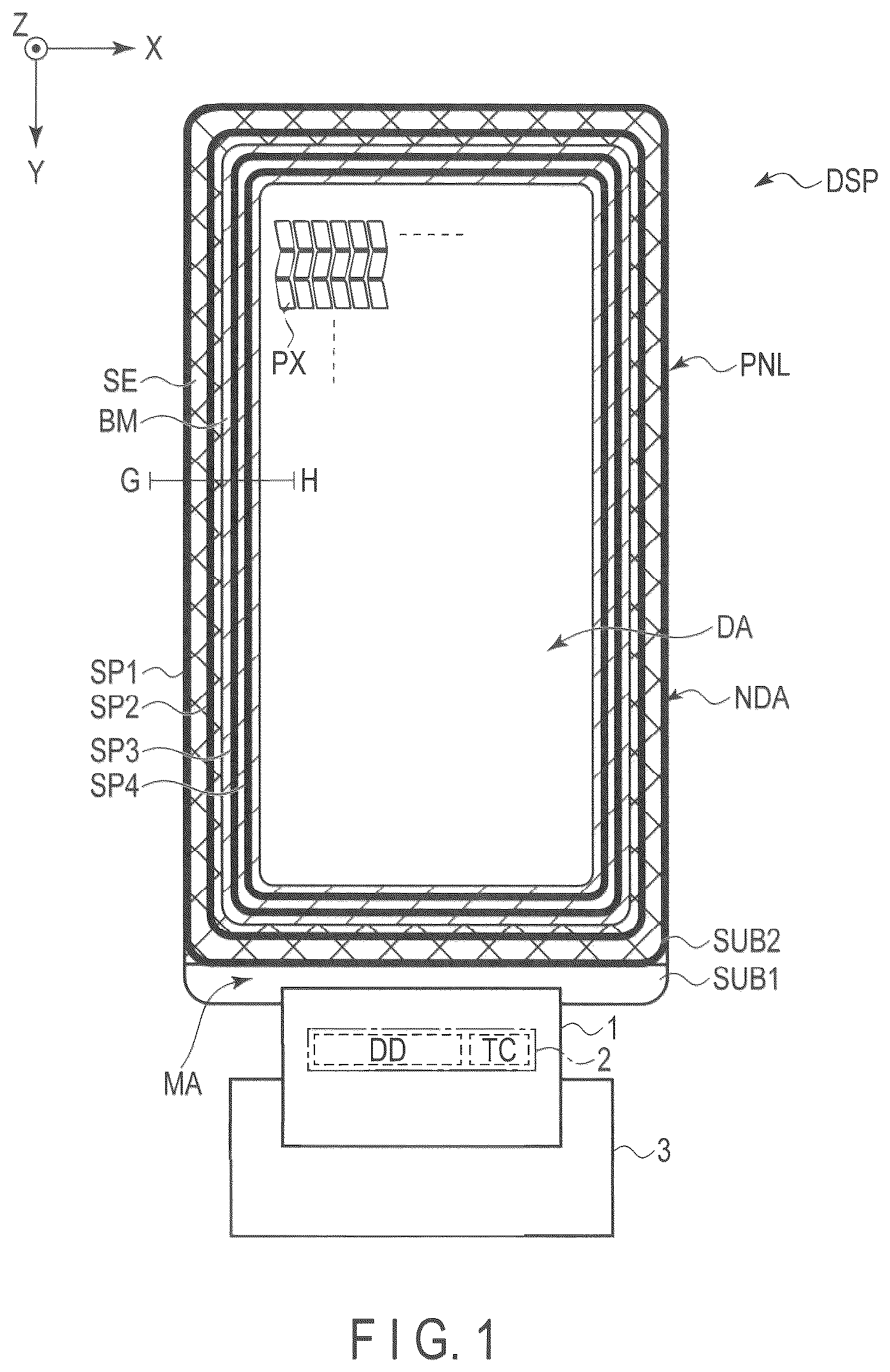
is a plan view showing an appearance of a display device DSP of each of the first to third embodiments.
For example, a first direction X, a second direction Y and a third direction Z are orthogonal to each other, but they may cross each other at an angle other than 90°. The first direction X and the second direction Y correspond to a direction parallel to the main surface of the substrate which constitutes the display device DSP, and the third direction Z corresponds to a thickness direction of the display device DSP. In this specification, the direction towards a distal end an arrow indicating the third direction Z is referred to as “above” (or merely “up”), and the direction towards opposite from the distal end of the arrow is referred to as “below” (or merely “down”). Further, an observation position where the display device DSP is observed is set on an distal end side of the arrow which indicates the third direction Z, and plan view is defined as a view from this observation position toward an X-Y plane defined by the first direction X and the second direction Y.
Here, a plan view of the display device DSP in the X-Y plane is shown. The display device DSP comprises a display panel PNL, a flexible printed circuit 1 , an IC chip 2 and a circuit board 3 .
The display panel PNL is a liquid crystal display panel, which comprises a first substrate SUB 1 , a second substrate SUB 2 , a sealing material SE, a light-shielding layer BM, spacers SP 1 to SP 4 and a liquid crystal layer LC, which will be described later. The display panel PNL includes a display area DA which displays images and a frame-like non-display area NDA which surrounds the display area DA. The second substrate SUB 2 opposes the first substrate SUB 1 . The first substrate SUB 1 includes a mounting portion MT extending in the second direction Y further from the second substrate SUB 2 .
The sealing material SE is provided in the non-display area NDA so as to adhere the first substrate SUB 1 and the second substrate SUB 2 to each other. The light-shielding layer BM is located in the non-display area NDA. The sealing material SE is provided in a position overlapping the light-shielding layer BM in plan view. In , the region where the sealing material SE is provided and the region where the light-shielding layer BM is provided are illustrated by slashes different from each other and the region where the sealing material SE and the light shielding layer BM overlap each other is illustrated by cross-hatching. The light-shielding layer BM is provided on the second substrate SUB 2 .
The spacers SP 1 to SP 4 are all located in the non-display area NDA. The spacer SP 1 is located in the outermost circumference of the display panel PNL. The spacer SP 2 is located on a display area DA side with respect to the spacer SP 1 . The spacers SP 1 and SP 2 overlap the sealing material SE. The spacers SP 3 and SP 4 are located on the display area DA side with respect to the sealing material SE. The spacers SP 1 to SP 4 are formed, for example, on the second substrate SUB 2 , but they may be provided on the first substrate SUB 1 .
The display area DA is located on an inner side surrounded by the light-shielding layer BM. The display area DA comprises, for example, a plurality of pixels PX arranged in a matrix along the first direction X and the second direction Y.
The flexible printed circuit 1 is mounted on the mounting portion MA, and is connected to the circuit board 3 . The IC chip 2 is mounted on the flexible printed circuit 1 . Note that the IC chip 2 may be mounted on the mounting portion MA. The IC chip 1 comprises a built-in display driver DD, which outputs signals necessary to display images in a display mode for displaying images. Moreover, in the example illustrated, the IC chip 2 contains a built-in touch controller TC which controls a touch sensing mode detecting approaching or contact of an object to the display device DSP. In the figures, the IC chip 2 is indicated by an alternate long and short dash line, whereas the display driver DD and the touch controller TC are indicated by dotted lines.
The display panel PNL of this embodiment may be any of a transmissive type comprising a transmissive display function which displays images by selectively transmitting light from a rear surface side of the first substrate SUB 1 , a reflective type comprising a reflective display function which displays images by selectively reflecting light from a front surface side of the second substrate SUB 2 and a trans-reflective type comprising both of the transmissive display function and the reflective display function.
An explanation of the detailed structure of the display panel PNL is omitted here, but the display panel PNL may have a structure provided for a display mode which uses a lateral electric field along a main surface of the substrate, a display mode which uses a vertical electric field along a normal of the main surface of the substrate, a display mode which uses an inclined electric field inclined in an oblique direction to the main surface of the substrate, and also a display mode which uses the lateral electric field, the vertical electric field and the inclined electric field in an appropriate combination. Here, the main surface of the substrate is a surface parallel to the X-Y plane defined by the first direction X and the second direction Y.
is a plan view showing a configuration example of a touch sensor TS. Here, a self-capacitive touch sensor TS will be described, but the touch sensor TS may be of a mutual capacitive mode.
The touch sensor TS comprises a plurality of sensor electrodes Rx (Rx 1 , Rx 2 , . . . ) arranged in a matrix and a plurality of sensor wiring lines L (L 1 , L 2 . . . ). The plurality of sensor electrodes Rx are located in the display area DA and arranged in the matrix along the first direction X and the second direction Y. One sensor electrode Rx constitutes one sensor block B. A sensor block B is the minimum unit in which touch sensing can be performed. The plurality of sensor wiring lines L, in the display area DA, each extend along the second direction Y, and are arranged along the first direction X. Each of the sensor wiring lines L is provided in the position overlapping, for example, a respective signal line S, which will be described later. Moreover, each of the sensor wiring lines L is drawn to the non-display area NDA, and is electrically connected to the IC chip 2 via the flexible printed circuit 1 . The sensor wiring lines L each comprise a terminal portion T in the non-display area NDA.
Here, the relationship between sensor wiring lines L 1 to L 3 arranged along the first direction X and sensor electrodes Rx 1 to Rx 3 arranged along in the second direction Y will be focused. The sensor wiring line L 1 overlaps the sensor electrodes Rx 1 to Rx 3 , and is electrically connected to the sensor electrode Rx 1 .
The sensor wiring line L 2 overlaps the sensor electrodes Rx 2 and Rx 3 , and is electrically connected to the sensor electrode Rx 2 . A dummy wiring line D 20 is provided to be spaced from the sensor wiring line L 2 . The dummy wiring line D 20 overlaps the sensor electrode Rx 1 , and is electrically connected to the sensor electrode Rx 1 . The sensor wiring line L 2 and the dummy wiring line D 20 are located on the same signal line.
The sensor wiring line L 3 overlaps the sensor electrode Rx 3 , and is electrically connected to the sensor electrode Rx 3 . A dummy wiring line D 31 is provided to overlap the sensor electrode Rx 1 , and is electrically connected to the sensor electrode Rx 1 . A dummy wiring line D 32 is provided to be spaced from the dummy wiring line D 31 and the sensor wiring line L 3 . The dummy wiring line D 32 overlaps the sensor electrode Rx 2 , and is electrically connected to the sensor electrode Rx 2 . The sensor wiring line L 3 and the dummy wiring lines D 31 and D 32 are located on the same signal line.
In the touch sensing mode, the touch controller TC applies a touch drive voltage to the sensor wiring lines L. Thus, the touch drive voltage is applied to the sensor electrodes Rx, and sensing by the sensor electrodes Rx is carried out. A sensor signal corresponding to the result of the sensing by the sensor electrodes Rx is output to the touch controller TC via the sensor wiring lines L. The touch controller TC or an external host detects whether there is an object approaching or contacting the display device DSP and position coordinates of the object based on the sensing signal.
In the display mode, the sensor electrodes Rx function as a common electrode CE to which a common voltage (Vcom) is applied. The common voltage is applied via the sensor wiring lines L from a voltage feeding portion contained in the display driver DD, for example.
is a plan view showing a sensor electrode Rx shown in and pixels PX. In , a direction intersecting the second direction Y counter-clockwise at an acute angle is defined as a direction D 1 , whereas a direction intersecting the second direction Y clockwise at an acute angle is defined as a direction D 2 . Note that an angle θ 1 made between the second direction Y and direction D 1 is substantially the same as an angle θ 2 made between the second direction Y and the direction D 2 .
One sensor electrode SE is disposed over a plurality of pixels PX. In the example illustrated, those of the pixels PX which are located in odd-numbered lines along the second direction Y each extend along the direction D 1 . On the other hand, those of the pixels PX which are located in even-numbered lines along the second direction Y each extend along the direction D 2 . Here, one pixel PX indicates the minimum unit which can be individually controlled according to a pixel signal, and it may be called a sub-pixel. Moreover, the minimum unit for realizing color display may be called a main pixel MP. The main pixel is configured to comprise a plurality of sub-pixels PX which exhibit different colors. For example, a min pixel MP comprises, as sub-pixels PX, a red pixel displaying red, a green pixel displaying green and a blue pixel displaying blue. Note that the main pixel MP may comprise a white pixel displaying white.
For example, in one sensor electrode Rx, sixty to seventy main pixels MP are arranged along the first direction X, and sixty to seventy main pixels MP are arranged along the second direction.
is a view illustrating a basic configuration and an equivalent circuit of a pixel PX.
A plurality of scanning lines G are connected to a scanning line drive circuit GD. A plurality of signal lines S are connected to a signal line drive circuit SD. The scanning lines G and the signal lines S may not extend linearly, but part of the lines may be bent. For example, the signal lines S extend along the second direction Y even if they are partially bent.
One common electrode CE is provided in each sensor block B. The common electrode CE is connected to a voltage supply portion CD of a common voltage (Vcom), and is disposed over a plurality of pixels PX. Moreover, the common electrodes CE are connected also to the touch controller TC as described above, and form the sensor electrodes Rx to which the touch drive voltage is applied in the touch sensing mode.
Each pixel PX comprises a switching element SW, a pixel electrode PE, a common electrode CE, a liquid crystal layer LC and the like. The switching element SW is constituted by, for example, a thin-film transistor (TFT) and is electrically connected to the respective scanning line G and the respective signal line S. The scanning line G is connected to the switching elements SW of the respective pixels PX arranged in the first direction X. The signal line S is connected to the switching elements SW of the respective pixels PX arranged in the second direction Y. The pixel electrodes PE are electrically connected to the respective switching elements SW. Each pixel electrode PE opposes the respective common electrode CE, and drives the liquid crystal layer LC by an electric field produced between the pixel electrode PE and the common electrode CE. A storage capacitor CS is formed between, for example, an electrode of the same potential as that of the common electrode CE and an electrode of the same potential as that of the pixel electrode PE.
is a plan view showing an example of layout of pixels.
The scanning lines G 1 to G 3 each extend linearly along the first direction X, and are arranged at intervals along the second direction Y. The signal lines S 1 to S 4 extend substantially along the second direction Y, and are arranged at intervals along the first direction X.
The pixel electrodes PE 1 and PE 2 are disposed between the scanning lines G 1 and G 2 . The pixel electrodes PE 1 and PE 2 are arranged along the first direction X. The pixel electrodes PE 3 and PE 4 are disposed between the scanning lines G 2 and G 3 . The pixel electrodes PE 3 and PE 4 are arranged along the first direction X. The pixel electrodes PE 1 and PE 3 are disposed between the signal lines S 1 and S 2 , and the pixel electrodes PE 2 and PE 4 are disposed between the signal lines S 2 and S 3 .
The pixel electrodes PE 1 and PE 2 comprise strip electrodes Pa 1 and Pa 2 , respectively, extending along the direction D 1 . The pixel electrodes PE 3 and PE 4 comprise strip electrodes Pa 3 and Pa 4 , respectively, extending along the direction D 2 . In the example illustrated, the number of each type of the strip electrodes Pa 1 to Pa 4 is two, but it may be one or three or more.
A common electrode (first common electrode) CE 1 is disposed over pixels PX 1 and PX 2 . A common electrode (second common electrode) CE 2 is disposed over pixels PX 3 and PX 4 . The common electrodes CE 1 and CE 2 are arranged along the second direction Y. The common electrodes CE 1 and CE 2 are contained in one sensor electrode Rx shown in . The common electrode CE 1 overlaps the scanning line G 1 and the signal lines S 1 to S 3 . The pixel electrodes PE 1 and PE 2 overlap the common electrode CE 1 . The common electrode CE 2 overlaps the scanning line G 3 and the signal lines S 1 to S 3 . The pixel electrodes PE 3 and PE 4 overlap the common electrode CE 2 . In the example illustrated, the scanning line G 2 are located between the common electrodes CE 1 and CE 2 .
A bridge portion BR is equivalent to a region indicated with slash in the figure. The bridge portion BR is located between the common electrode CE 1 and the common electrode CE 2 and overlaps the signal line S 2 . The bridge portion BR is formed to be integrated with the common electrode CE 1 and the common electrode CE 2 into one body, and electrically connects the common electrode CE 1 and the common electrode CE 2 to each other. The bridge portion BR is contained in the sensor electrode Rx as in the case of the common electrode CE 1 and the common electrode CE 2 .
is a plan view showing an example of the pixel PX shown in . Here, the main part will be described while focusing on the pixel PX 1 surrounded by the scanning lines G 1 and G 2 and the signal lines S 1 and S 2 shown in .
The switching element SW is electrically connected to the scanning line G 2 and the signal line S 2 . The switching element SW comprises a semiconductor layer SC and a drain electrode (first drain electrode) DE 1 .
The semiconductor layer SC is disposed so that one part thereof overlaps the signal line S 2 and the other parts extends between the signal lines S 1 and S 2 to form substantially a U shape. The semiconductor layer SC intersects the scanning line G 2 in the position where it overlaps the signal line S 2 and intersects the scanning line G 2 also between the signal lines S 1 and S 2 . In the scanning line G 2 , the region overlapping the semiconductor layer SC functions as the gate electrodes GE 1 and GE 2 . That is, in the example illustrated, the switching element SW has a double-gate structure. The semiconductor layer SC is electrically connected by its one end portion SCA to the signal line S 2 via a through-hole CH 1 , and by its other end portion SCB, electrically connected to the drain electrode DE 1 via a through-hole CH 2 .
The drain electrode DE 1 is formed into an island-like shape, and is disposed between the signal line S 1 and the signal line S 2 . Note that in the switching element SW, the drain electrode DE 1 may be referred to as a source electrode.
The pixel electrode PE 1 comprises a base BS 1 integrated with the plurality of strip electrodes Pa 1 . The base BS 1 overlaps the drain electrode DE 1 , and is electrically connected to the drain electrode DE 1 . A connecting portion between the pixel electrode PE 1 and the switching element SW will be described later.
is a cross-sectional view of the first substrate SUB 1 taken along line A-B shown in .
The first substrate SUB 1 comprises an insulating substrate 10 , insulating films 11 to 16 , a semiconductor layer SC, a scanning line G 2 , a signal line S 2 , a metal wire ML 2 , a common electrode CE 1 , a bridge portion BR, an alignment film AL 1 and the like.
The insulating substrate 10 is a light transmissive substrate such as a glass substrate or a flexible resin substrate. The insulating film 11 is located on the insulating substrate 10 . The semiconductor layer SC is located on the insulating film 11 , and is covered by an insulating film 12 . The semiconductor layer SC is formed of, for example, polycrystalline silicon, but may be formed of amorphous silicon or an oxide semiconductor.
The gate electrode GE 1 , which is a part of the scanning line G 2 , is located on the insulating film 12 , and is covered by the insulating film 13 . Note that the other scanning lines which are not illustrated are located in the same layer as that of the scanning line G 2 . The scanning line G 2 is formed of a metal material such as aluminum (Al), titanium (Ti), silver (Ag), molybdenum (Mo), tungsten (W), copper (Cu) or chromium (Cr), or an alloy of any combination of these metal materials, and it may be of a single- or multi-layer structure. For example, the scanning line G 2 is formed from a molybdenum-tungsten alloy.
The signal line S 2 is located on the insulating film 13 and is covered by an insulating film (first insulating film) 14 . Note that the other signal lines which are not illustrated are located in the same layer as that of the signal line S 2 . The signal line S 2 is formed of a metal material of those listed above or an alloy of any combination thereof, and it may be of a single- or multi-layer structure. For example, the signal line S 2 is a stacked layered body in which the first layer containing titanium (Ti), the second layer containing aluminum (Al) and the third layer containing titanium (Ti) are stacked in this order. The signal line S 2 is in contact with the semiconductor layer SC via a through-hole CH 11 which penetrates the second insulating film 12 and the third insulating film 13 .
The metal wire ML 2 is located on the insulating film 14 , and is covered by the insulating film (second insulating film) 15 . The metal wire ML 2 is formed of a metal material of those listed above or an alloy of any combination thereof, and it may be of a single- or multi-layer structure. For example, the metal wire ML 2 is a layered body in which the first layer containing titanium (Ti), the second layer containing aluminum (Al) and the third layer containing titanium (Ti), or the first layer containing molybdenum (Mo), the second layer containing aluminum (Al) and the third layer containing molybdenum (Mo) are stacked in this order.
The common electrode CE 1 and the bridge portion BR are located on the insulating film 15 , and are covered by the insulating film (third insulating film) 16 . The common electrode CE and the bridge portion BR are transparent electrodes each formed of a transparent conductive material such as indium tin oxide (ITO) or indium zinc oxide (IZO). The common electrode CE 1 is in contact with the metallic wire ML 2 via a through-hole CH 3 which penetrates the insulating film 15 . The alignment film AL 1 is located on the insulating film 16 .
The insulating films 11 to 13 and the insulating film 16 are inorganic insulating films each formed from an inorganic insulating material such as a silicon oxide, silicon nitride or silicon oxynitride, and they may be of a single- or multi-layer structure. The insulating films 14 and 15 are organic insulating films each formed of an organic insulating material, for example, an acrylic resin.
As described above, the common electrode CE 1 functions as a sensor electrode Rx and a metal wire ML 2 functions as a sensor wire L electrically connected to the sensor electrode Rx.
is a cross-sectional view showing the display panel PNL seen along line C-D in . The example illustrated is the case where a display mode using a lateral electric field is applied.
In the first substrate SUB 1 , the signal lines S 1 and S 2 are located on the insulating film 13 , and are covered by the insulating film 14 . The metal wires ML 1 and ML 2 are located immediately above the signal lines S 1 and S 2 , respectively. The pixel electrode PE 1 is disposed on the insulating film 16 and is covered by the alignment film AL 1 . The pixel electrode PE is a transparent electrode formed of a transparent, electrically conductive material such as ITO or IZO.
The second substrate SUB 2 comprises a second insulating substrate 20 , a light-shielding layer BM, a color filter CF, an overcoat layer OC, an alignment film AL 2 and the like.
As in the case of the insulating substrate 10 , the insulating substrate 20 is a light transmissive substrate such as a glass substrate or a resin substrate. The light-shielding layer BM and the color filter CF are located on a side of the insulating substrate 20 , which oppose the first substrate SUB 1 . The color filter CF is disposed at a position opposing the pixel electrode PE 1 , and partially overlaps the light-shielding layer BM. The color filter CF includes a red color filter CFR, a green color filter CFG and a blue color filter CFB. The overcoat layer OC covers the color filter CF. The overcoat layer OC is formed of a transparent resin material. The alignment film AL 2 covers the overcoat layer OC. The alignment film AL 1 and the alignment film AL 2 are formed of, for example, a material which exhibits horizontal alignment properties.
The first substrate SUB 1 and the second substrate SUB 2 described above are disposed such that the alignment film AL 1 and the alignment film AL 2 oppose each other. The first substrate SUB 1 and the second substrate SUB 2 are adhered to each other with a predetermined cell gap formed therebetween. The liquid crystal layer LC is held between the alignment film AL 1 and the alignment film AL 2 . The liquid crystal layer LQ contains liquid crystal molecules LM. The liquid crystal layer LC is formed from a positive type (positive dielectric constant anisotropy) or a negative type (negative dielectric constant anisotropy) liquid crystal material.
An optical element OD 1 including a polarizer PL 1 is adhered to the insulating substrate 10 . An optical element OD 2 including a polarizer PL 2 is adhered onto the insulating substrate 20 . Note that the optical element OD 1 and the optical element OD 2 may comprise a retardation film, a scattering layer, an antireflective layer or the like when necessary.
In the display panel PNL with such a configuration, the liquid crystal molecules LM are initially aligned in a predetermined direction between the alignment film AL 1 and the alignment film AL 2 in an OFF state in which an electric field is not formed between the pixel electrode PE and the common electrode CE. In the OFF state as such, light irradiated from an illumination device IL towards the display panel PNL is absorbed by the optical element OD 1 and the optical element OD 2 , thus creating dark display. On the other hand, in the ON state in which an electric field is formed between the pixel electrode PE and the common electrode CE, the liquid crystal molecules LM is aligned by the electric field in a direction different the direction in the initial alignment, and the direction of alignment is controlled by the electric field. In the ON state as such, part of the light from the illumination device IL passes through the optical element OD 1 and the optical element OD 2 , thus creating bright display.
Next, the display device DSP according to the first embodiment will be described in detail.
is a detailed plan view showing the vicinity of the bridge portion BR in the pixel layout in . The pixel PX 1 comprises a pixel electrode PE 1 , a drain electrode DE 1 , a first metal electrode ME 1 and a first transparent electrode TE 1 . The first metal electrode ME 1 and the first transparent electrode TE 1 overlap the base BS 1 and the drain electrode DE 1 to form a connection portion CN 1 which electrically connects the pixel electrode PE 1 and the drain electrode DE 1 to each other. The pixel PX 2 comprises a pixel electrode PE 2 , a drain electrode (second drain electrode) DE 2 , a second metal electrode ME 2 and a second transparent electrode TE 2 . The drain electrodes DE 1 and DE 2 are arranged along the first direction X. The second metal electrode ME 2 and the second transparent electrode TE 2 overlap the base BS 2 and the drain electrode DE 2 to form a connection portion CN 2 which electrically connects the pixel electrode PE 2 and the drain electrode DE 2 to each other.
As will be described later, the common electrodes CE 1 and CE 2 , the first transparent electrode TE 1 , the second transparent electrode TE 2 and the bridge portion BR are disposed in the same layer. The first transparent electrode TE 1 and the second transparent electrode TE 2 are arranged along the first direction X between the common electrode CE 1 and the common electrode CE 2 . The bridge portion BR is located between the first transparent electrode TE 1 and the second transparent electrode TE 2 .
The metal wires ML 1 to ML 3 overlap the signal lines S 1 to S 3 , respectively. The metal wire ML 2 comprises a line portion LP and a pedestal portion 100 in a position overlapping the bridge portion BR. The line portion LP has a width W 1 . The pedestal portion 100 has a width W 2 . The width W 2 is greater than the width W 1 . The metal wire ML 2 is electrically connected to the bridge portion BR in the pedestal portion 100 . That is, the pedestal portion 100 is in contact with the bridge portion BR in the through-hole which overlaps the pedestal portion 100 . The pedestal portion 100 is formed to be broad so as to secure the region to be in contact with the bridge portion BR. The metal electrode ML 2 is electrically connected to the common electrodes CE 1 and CE 2 via the bridge portion BR.
is a plan view showing positions of light-shielding layer BM, the metal wires ML 1 to ML 3 , the first metal electrode ME 1 and the second metal electrode ME 2 , which correspond to the pixel layout in .
The first metal electrode ME 1 is located between the metal wire ML 1 and the metal wire ML 2 . The second metal electrode ME 2 is located between the metal wire ML 2 and the metal wire ML 3 . The pedestal portion 100 of the metal wire ML 2 is located between the first metal electrode ME 1 and the second metal electrode ME 2 . For example, the width W 2 of the pedestal portion 100 is about 7.6 μm. Moreover, for example, the width of the first metal electrode ME 1 and the second metal electrode ME 2 , taken along the first direction X, is about 8.0 μm.
As will be discussed later, the through-holes CH 11 and CH 12 penetrate the insulating film 14 , and a through-hole CH 23 penetrates the insulating film 15 . The through-hole CH 11 is formed in a position overlapping the first metal electrode ME 1 . The through-hole CH 12 is formed in a position overlapping the second metal electrode ME 2 . The through-hole CH 23 is located between the first metal electrode ME 1 and the second metal electrode ME 2 , and is formed in a position overlapping the pedestal portion 100 . The width of the through-hole CH 23 along the first direction X is about 4 μm.
The through-hole CH 11 is located approximately at a center between the metal wire ML 1 and the metal wire ML 2 in plan view. The first metal electrode ME 1 has a width (first width) W 11 on a side of the pedestal portion 100 with respect to the through-hole CH 11 , and a width (second width) W 12 on an opposite side to the pedestal portion 100 with respect to the through-hole CH 11 . The width W 2 is greater than the width W 1 . That is, the first metal electrode ME 1 is disposed closer to the metal wire ML 1 as compared to the metal ire ML 2 .
The through-hole CH 12 is located approximately at a center between the metal wires ML 2 and ML 3 in plan view. The second metal electrode ME 2 has a width (third width) W 13 on a side of the pedestal portion 100 with respect to the through-hole CH 12 and a width (fourth width) W 14 on an opposite side to the pedestal portion 100 with respect to the through-hole CH 12 . The width W 14 is greater than the width W 13 . That is, the second metal electrode ME 2 is disposed closer to the metal wire ML 3 as compared to the metal wire ML 2 . Therefore, the first metal electrode ME 1 and the second metal electrode ME 2 are disposed on one side so as to be spaced from the pedestal portion 100 .
The light-shielding layer BM is formed into a grid shape, and overlaps each of the scanning lines G 1 to G 3 , the signal lines S 1 to S 3 , the metal wires ML 1 to ML 3 , the connection portions CN 1 and CN 2 , the bases BS 1 and BS 2 and the drain electrodes DE 1 and DE 2 , shown in . The light-shielding layer BM includes a first portion BM 11 extending in the first direction X, and second portions BM 21 to BM 23 extending in the second direction Y. The first portion BM 11 has a width W 21 along in the second direction Y, and the second portions BM 21 to BM 23 each have a width W 22 along the first direction X. The width W 21 is greater than the width W 22 . The first portion BM 11 overlaps the pedestal portion 100 , the first metal electrode ME 1 , the second metal electrode ME 2 and the through-holes CH 11 , CH 23 and CH 12 .
According to this embodiment, the first metal electrode ME 1 and the second metal electrode ME 2 are disposed on one side which is spaced apart from the metal wire ML 2 . With this configuration, the pedestal portion 100 can be disposed between the first metal electrode ME 1 and the second metal electrode ME 2 . In other words, the pedestal portion 100 can be placed in the position overlapping the first portion BM 11 of the light-shielding layer BM. For example, when the pedestal portion 100 is disposed in the position overlapping the second portion BM 22 of the light-shielding layer BM, light reflected in the pedestal portion 100 may leak from both sides of the second portion BM 22 . In this embodiment, the pedestal portion 100 is located in the position overlapping the first portion BM 1 having a width greater than that of the second portion BM 22 , the leakage of light from around the pedestal portion 100 can be inhibited. Therefore, the degrading of the contrast of the display device caused by leakage of light can be suppressed. Thus, deterioration in display quality can be suppressed.
is a cross-sectional view of the first substrate SUB 1 taken along line E-F in . Note that in the first substrate SUB 1 shown, the layers below the insulating film 13 and the alignment film AL 1 omitted from the illustration. Moreover, also shows a plan view of each of the first transparent electrode TE 1 , the second transparent electrode TE 2 and the bridge portion BR, which corresponds to the section.
The first substrate SUB 1 includes the drain electrodes DE 1 and DE 2 , the signal lines S 1 to S 3 , the first metal electrode ME 1 , the second metal electrode ME 2 , the first transparent electrode TE 1 , the second transparent electrode TE 2 , the metal wires ML 1 to ML 3 , the insulating films 13 to 16 , the pixel electrodes PE 1 and PE 2 and the bridge portion BR.
The signal lines S 1 to S 3 and the drain electrodes DE 1 and DE 2 are located on the insulating film 13 , and are covered by the insulating film 14 . The drain electrodes DE 1 and DE 2 are located in the same layer as that of the signal lines S 1 to S 3 , and are formed of a material identical to that of the signal lines S 1 to S 3 .
The insulating film 14 comprises the through-hole (first through-hole) CH 11 which penetrates to the drain electrode DE 1 , and the through-hole (fifth through-hole) CH 12 which penetrates to the drain electrode DE 2 .
The metal wires ML 1 to ML 3 , the first metal electrode ME 1 and the second metal electrode ME 2 are located on the insulating film 14 , and they are covered by the insulating film 15 . The first metal electrode ME 1 is in contact with the drain electrode DE 1 in the through-hole CH 11 . Similarly, the second metal electrode ME 2 is in contact with the drain electrode DE 2 in the through-hole CH 12 . The first metal electrode ME 1 and the second metal electrode ME 2 are located in the same layer as that of the metal wires ML 1 to ML 3 , and they are formed of a metal material identical to that of the metal wires ML 1 to ML 3 . The metal wires ML 1 to ML 3 are located immediately above the signal lines S 1 to S 3 , respectively.
As shown in , the first metal electrode ME 1 and the second metal electrode ME 2 are displaced to a side spaced away from the metal wire ML 2 . The first metal electrode ME 1 , the second metal electrode ME 2 and the pedestal portion 100 are located in the same layer, and with such a layout, short-circuiting between the first metal electrode ME 1 and the pedestal portion 100 and that between the second metal electrode ME 2 and the pedestal portion 100 can be suppressed.
The insulating film 14 is scraped when the metal wires ML 1 to ML 3 , the first metal electrode ME 1 and the second metal electrode ME 2 are subjected to dry etching. Therefore, a difference in level is created in the insulating film 14 between a region where the film overlaps the metal wires ML 1 to ML 3 , the first metal electrode ME 1 and the second metal electrode ME 2 , and another region where it does not overlap these.
The insulating film 15 is located on the insulating film 14 , and comprises a through-hole (second through-hole) CH 21 which penetrates to the first metal electrode ME 1 , a through-hole (sixth through-hole) CH 22 which penetrates to the second metal electrode ME 2 , and a through-hole (fourth through-hole) CH 23 which penetrates to the pedestal portion 100 . The width of the through-hole CH 21 is less than the width of the through-hole CH 11 , and the width of the through-hole CH 22 is less than the width of the through-hole CH 12 .
The first transparent electrode TE 1 and the second transparent electrode TE 2 and the bridge portion BR are located on the insulating film 15 , and are covered by the insulating film 16 . The first transparent electrode TE 1 is in contact with the first metal electrode ME 1 in the through-hole CH 21 . Similarly, the second transparent electrode TE 2 is in contact with the second metal electrode ME 2 in the through-hole CH 22 . The bridge portion BR is in contact with the pedestal portion 100 in the through-hole CH 23 . The first transparent electrode TE 1 , the second transparent electrode TE 2 and the bridge portion BR are located in the same layer as that of the common electrodes CE 1 and CE 2 shown in , and are formed of a transparent conductive material as that of the common electrodes CE 1 and CE 2 .
The through-hole CH 21 is located approximately at a center between the metal wire ML 1 and the metal wire ML 2 . The first transparent electrode TE 1 has a width (fifth width) W 15 on a side of the bridge portion BR with respect to the through-hole CH 21 and a width (sixth width) W 16 on a side opposite to the bridge portion BR with respect to the through-hole CH 21 . The width W 16 is greater than the width W 16 . In other words, the first transparent electrode TE 1 is displaced to a side spaced away from the bridge portion BR with respect to the through-hole CH 21 .
The through-hole CH 22 is located approximately at a center between the metal wire ML 2 and the metal wire ML 3 . The second transparent electrode TE 2 has a width (seventh width) W 17 on a side of the bridge portion BR with respect to the through-hole CH 22 , and a width (eighth width) W 18 on an opposite side to the bridge portion BR with respect to the through-hole CH 22 . The width W 18 is greater than the width W 17 . That is, the second transparent electrode TE 2 is displaced to a side spaced away from the bridge portion BR with respect to the through-hole CH 22 .
As described above, the first transparent electrode TE 1 and the second transparent electrode TE 2 are displaced to the side spaced away from the bridge portion BR. The first transparent electrode TE 1 , the second transparent electrode TE 2 and the bridge portion BR are located in the same layer, and with such a layout, short-circuiting between the first transparent electrode TE 1 and the bridge portion BR and that between the second transparent electrode TE 2 and the bridge portion BR can be suppressed.
The insulating film 16 is located on the insulating film 15 , and comprises a through-hole (third through-hole) CH 31 which penetrates to the first transparent electrode TE 1 , and a through-hole CH 32 which penetrates to the second transparent electrode TE 2 . The through-hole CH 31 is located on one side which is spaced away from the bridge portion BR with respect to the through-holes CH 11 and CH 21 . The through-hole CH 32 is located on one side which is spaced away from the bridge portion BR with respect to the through-holes CH 12 and CH 22 .
The base BS 1 of the pixel electrode PE 1 and the base BS 2 of the pixel electrode PE 2 are located on the insulating film 16 , and are covered by the alignment film AL 1 (not shown). The pixel electrode PE 1 is in contact with the first transparent electrode TE 1 in the through-hole CH 31 . Similarly, the pixel electrode PE 2 is in contact with the second transparent electrode TE 2 in the through-hole CH 32 .
In the through-hole CH 11 , the stacked layer bodies SB 1 and SB 2 are disposed. The stacked layer body SB 1 includes the drain electrode DE 1 , the first metal electrode ME 1 , the first transparent electrode TE 1 and the pixel electrode PE 1 staked one on another in this order. The stacked layer body SB 2 includes the drain electrode DE 1 , the first metal electrode ME 1 , the first transparent electrode TE 1 , the insulating film 16 and the pixel electrode PE 1 stacked one on another in this order. In the example illustrated, the stacked layer body SB 1 is located on a side close to the signal line S 1 and the metal wire ML 1 , and the stacked layer body SB 2 is located on a side close to the signal line S 2 and the metal wire ML 2 .
The insulating film 15 comprises an end portion 151 E located between the first metal electrode ME 1 and the first transparent electrode TE 1 in a region between a set of the signal line S 1 and the metal wire ML 1 and the through-hole CH 21 . The pixel electrode PE 1 is in contact with the first transparent electrode TE 1 in a region immediately above the end portion 151 E. Similarly, the insulating film 15 comprises an end portion 152 E located between the second metal electrode ME 2 and the second transparent electrode TE 2 in a region between a set of the signal line S 3 and the metal wire ML 3 and the through-hole CH 22 . The pixel electrode PE 2 is in contact with the second transparent electrode TE 2 in a region immediately above the end portion 152 E.
As described above, according to the first embodiment, a display device which can suppress degradation of the image quality can be provided.
Next, a display device of the second embodiment will be explained in detail.
is a cross-sectional view showing a display panel PNL taken along line G-H in . shows a non-display area NDA of the display panel PNL.
The first substrate SUB 1 comprises peripheral wires WR 1 to WR 3 in the non-display area NDA. The peripheral wire WR 1 is disposed on the insulating film 12 and is covered by the insulating film 13 . The peripheral wire WR 1 is disposed in the same layer as that of the scanning line, and is formed from a material identical to that of the scanning line. The peripheral wire WR 2 is disposed on the insulating film 13 , and is covered by the insulating film 14 . The peripheral wire WR 2 is disposed in the same layer as that of the signal line and is formed from a material identical to that of the signal line. The peripheral wire WR 3 is disposed on the insulating film 16 , and is covered by the alignment film AL 1 . The peripheral wire WR 3 is disposed in the same layer as that of the pixel electrode, and is formed from a material identical to that of the pixel electrode.
The first substrate SUB 1 comprises a groove GR 1 which penetrates the insulating film 15 to the insulating film 14 in the non-display area NDA. The groove GR 1 is located on a side of the display area DA with respect to the sealing material SE. Further, the first substrate SUB 1 comprises a groove GR 2 which penetrates the insulating films 14 and 15 to the insulating film 13 in the non-display area NDA. The groove GR 2 overlaps the sealing material SE.
The insulating film 16 is disposed on the insulating film 15 , and also inside the groove GR 1 and the groove GR 2 . The insulating film 16 is in contact with a side surface and a bottom surface of the groove GR 1 , and is in contact with a side surface of the groove GR 2 . A difference in level is created in the side surface of the groove GR 2 by the insulating films 14 and 15 , and therefore the insulating film 16 easily adheres to the side surface of the groove GR 2 .
The alignment film AL 1 is disposed on the peripheral wire WR 3 and also inside the groove GR 1 and the groove GR 2 . In a region which overlaps the sealing material SE, the alignment film AL 1 is not disposed on the insulating film 15 . Thus, the sealing material SE is in contact with the insulating film 16 . For example, if the alignment film AL 1 is placed under the sealing material SE, the adhesion strength between the alignment film AL 1 and the insulating film 16 becomes weak, thereby possibly causing the peeling-off.
In this embodiment, the first substrate SUB 1 comprises a groove GR 1 located on a side of the display area DA with respect to the sealing material SE. With this configuration, even if the material of the printed alignment film AL 1 flows to the sealing material SE side, the flowing portion can be stopped by the groove GR 1 , and thus it is possible to inhibit the flow from reaching the region which overlaps the sealing material SE. Moreover, even if the frame of the display device DSP can be narrowed, it is still possible to inhibit the material of the alignment film AL 1 from flowing under the sealing material SE. Thus, the lowering of the adhesion strength between the first substrate SUB 1 and the second substrate SUB 2 can be suppressed and the entering of moisture from the interface created by the peeling-off can be inhibited.
In order to stop the flow of the material alignment film AL 1 within the groove GR 1 , the depth of the groove GR 1 should preferably be 0.2 μm or more. In this embodiment, the depth of the groove GR 1 is, for example, about 1.5 μm.
Further, in this embodiment, the first substrate SUB 1 comprises two layers, namely, the insulating films 14 and 15 , each formed of an organic insulating material. Therefore, of the two organic insulating films, the groove GR 1 is formed to penetrate the insulating film 15 , which is closer to the liquid crystal layer LC. As compared to the case where a groove portion is formed by carrying out half exposure on one organic insulating film, in this embodiment, the side surface of the groove GR 1 can be formed steep to the bottom surface. Since the form of the side surface of the groove GR 1 is steep, it is possible to inhibit the material of the alignment film AL 1 from flowing and running onto the region under the sealing material SE. Moreover, in order to stop the sealing material SE more reliably by the groove GR 1 , the groove GR 1 can be deepened to such an extent that it does not penetrate the insulating film 14 .
Moreover, with the groove GR 2 , the entering path of moisture migrating from the outside of the display panel PNL through the insulating films 14 and 15 can be blocked.
The light-shielding layer BM comprises a slit SL 1 penetrating to the second insulating substrate 20 . The entering path of moisture migrating in the light-shielding layer BM can be blocked by the slit SL 1 . Note that the first substrate SUB 1 comprises, in a position which overlaps the slit SL 1 , a peripheral wire WR 1 , and with this configuration, the leakage of light from the slit SL 1 can be inhibited.
The light-shielding layer BM comprises a slit SL 2 in the region which overlaps the liquid crystal layer LC. With this configuration, the migration path of electric charge to the display area DA via the light-shielding layer BM can be blocked in the slit SL 2 . Thus, it is possible to inhibit static electricity form concentrating on the display area DA in the manufacturing process of the display panel PNL, and to suppress damaging to the display panel PNL. Note that the first substrate SUB 1 comprises, in the position which overlaps the slit SL 2 , a peripheral wire WR 2 , and with this configuration, the leakage of light from the slit SL 2 can be suppressed. Moreover, the color filters CFR and CFB are disposed in the slit SL 2 to overlap each other in the third direction Z. Thus, the leakage of light from the slit SL 2 can be suppressed also against the light portion passing through around the peripheral wire WR 2 .
Spacers SP 1 to SP 4 are disposed on the second substrate SUB 2 and project out to a side of the first substrate SUB 1 . The spacers SP 1 to SP 4 are each formed of, for example, a resin material. Further, a color filter CFB for height adjustment is provided in the position which overlaps the spacers SP 1 and SP 2 . The liquid crystal layer LC is surrounded by the first substrate SUB 1 , the second substrate SUB 2 and the sealing material SE.
is a plan view indicating positions of the grooves GR 1 and GR 2 shown in .
The groove GR 1 includes portions GR 11 and GR 12 extending in the second direction Y, and a portion GR 13 extending in the first direction X. The portions GR 11 and GR 12 are each connected to the portion GR 13 . In this embodiment, the groove GR 1 should preferably have a width of 100 μm. The groove GR 1 is not formed between the display area DA and the mounting portion MA. On the mounting portion MA side, the distance from the display area DA to the sealing material SE is great, the alignment film AL 1 does not reach the sealing material SE. With this configuration, on the mounting portion MA side of the display area DA, the groove GR 1 for stopping the alignment film AL 1 need not be formed. The groove GR 2 includes portions GR 21 and GR 22 extending in the second direction Y, and portions GR 23 and GR 24 extending in the first direction X. The portions GR 21 and GR 22 are connected to the portions GR 23 and GR 24 , respectively.
is a cross section showing a modified example of the display panel PNL according to the second embodiment shown in . The structure shown in is different from that of in that a peripheral electrode (first peripheral electrode) PRE 1 is disposed under the sealing material SE.
The peripheral electrode PRE 1 is located between the sealing material SE and the insulating film 16 . The peripheral electrode PRE 1 is disposed in the same layer as that of the peripheral wire WR 3 and the pixel electrode, and is formed from a material identical to that of these members. With the peripheral electrode PRE 1 disposed under the sealing material SE, the adhesion strength of the sealing material SE can be enhanced, and the electric field from the peripheral wire WR 1 can be shielded.
With this configuration, an advantageous effect similar to that of the example shown in can be obtained.
is a cross section showing a modified example of the display panel PNL according to the second embodiment shown in . The structure shown in is different from that of in that the peripheral electrode (second peripheral electrode) PRE 2 is disposed in a position overlapping the sealing material SE.
The peripheral electrode PRE 2 is disposed on the insulating film 15 , and is covered by the insulating film 16 . The peripheral electrode PRE 2 is disposed in the same layer as that of the common electrode, the first transparent electrode and the second transparent electrode, and is formed from a material identical to that of these members. With the peripheral electrode PRE 2 disposed in the position overlapping the sealing material SE, the adhesion strength of the sealing material SE can be enhanced and the electric field from the peripheral wire WR 1 can be shielded.
With this configuration, an advantageous effect similar to that of the example shown in can be obtained.
is an enlarged view of a region I and a region J shown in .
, part (a) shows an enlarged view of the region I. The portion GR 11 of the groove GR 1 has a width W 31 along the first direction X. The width W 31 is about 150 μm. The portion GR 12 shown in has a width similar to that of the portion GR 11 . The peripheral wire WR 3 extends in the second direction Y between the portion GR 11 and the display area DA.
, part (b) shows an enlarged view of the region J. The portion GR 13 has a width W 32 along the second direction Y. The width W 32 is greater than the width W 31 . The width W 32 is about 350 μm. The peripheral wire WR 3 extends in the first direction X between the portion GR 13 and the display area DA.
As described above, according to the second embodiment, a display device which can suppress degradation of the reliability can be provided.
Next, a display device according to a third embodiment will be explained in detail.
is a plan view showing a comparative example of the terminal portion T of the sensor wire L shown in .
A through-hole CH 61 is located in a region overlapping the terminal portion T. The through-hole CH 61 has a width W 41 along the first direction X, and a width W 42 along the second direction Y. For example, the width W 41 is about 5 μm, and the width W 42 is about 10 μm. The through-hole CH 61 comprises side surfaces SS 1 to SS 4 .
is a cross-sectional view of the first substrate SUB 1 taken along line K-M in .
The through-hole CH 61 penetrates the insulating film 14 to the peripheral wire WR 2 . In the comparative example shown in , an angle θ 11 between the side surface SS 1 and the peripheral wire WR 2 and an angle θ 12 between the side surface SS 2 and the peripheral wire WR 2 are greater than 90°. With this structure, the terminal portion T cannot follow up the side surfaces SS 1 and SS 2 , but is disconnected. Note that this is also the case for the side surfaces SS 3 and SS 4 shown in .
is a plan view showing a terminal portion T according to the third embodiment. The structure shown in is different from that of in that a through-hole (seventh through-hole) CH 71 and a through-hole (eighth through-hole) CH 72 are different from that in width.
The through-holes CH 71 and CH 72 are located in a region overlapping the terminal portion T. The through-holes CH 71 and CH 72 each have a width W 51 along the first direction X and a width W 52 along the second direction Y. The width W 51 is less than the width W 41 of the through-hole CH 61 shown in , and the width W 52 is less than the width W 42 . For example, the width W 51 and the width W 52 are each about 3.5 μm. The through-hole CH 71 comprises side surfaces SS 11 to SS 14 , and the through-hole CH 72 comprises side surfaces SS 15 to SS 18 .
In this embodiment, the width W 51 is approximately equal to the width of the through-hole CH 11 along the first direction X shown in , and the width W 52 is approximately equal to the width of the through-hole CH 11 along the second direction Y.
is a cross-sectional view of the first substrate SUB 1 taken along line N-O shown in .
The through-holes CH 71 and CH 72 penetrate the insulating film 14 to the peripheral wire (the first peripheral wire) WR 2 . In the third embodiment, the angle θ 21 between the side surface SS 11 and the peripheral wire WR 2 , the angle θ 22 between the side 12 and the peripheral wire WR 2 , the angle θ 23 between the side surface SS 15 and the peripheral wire WR 2 , and the angle θ 24 between the side surface SS 16 and the peripheral wire WR 2 are 90° or less. With this configuration, the terminal portion T follows the side surface SS 11 , SS 12 , SS 15 and SS 16 , and is electrically connected to the peripheral wire WR 2 in the through-holes CH 71 and CH 72 . Nota that this is also the case for the side surfaces SS 13 , SS 14 , SS 17 and SS 18 shown in .
Thus, the width of the through-holes CH 71 and CH 72 which overlap the terminal portion T is set equivalent to the width of the through-hole CH 21 of the display area DA, and therefore disconnection of the terminal portion T can be inhibited.
In the example illustrated, two through-holes CH 71 and CH 72 are formed in the region which overlaps the terminal portion T, but the number of through-holes may be one or three or more.
is a plan view showing a comparative example of the peripheral wire WR 3 in the region U shown in .
Through-holes CH 81 and CH 82 are located in the region which overlaps the peripheral wire WR 3 and the metal electrode ME. The through-hole CH 81 comprises a width W 61 along the first direction X, and a width W 62 along the second direction Y. The through-hole CH 82 comprises a width W 71 along the first direction X, and a width W 72 along the second direction Y. For example, the width W 61 and the width W 71 are approximately the same and each are about 5 μm, and the width W 62 and the width W 72 are approximately the same and each are about 10 μm. The through-hole CH 81 comprises side surfaces SS 21 to SS 24 . The through-hole CH 82 comprises side surfaces SS 25 to SS 28 .
is a cross-sectional view of the first substrate SUB 1 taken along line P-Q shown in .
The metal electrode ME is located between the insulating film 14 and the insulating film 15 . The through-hole CH 81 penetrates the insulating film 14 to the peripheral wire WR 2 . The through-hole CH 82 penetrates the insulating film 15 to the metal electrode ME. In the through-hole CH 81 , an angle θ 31 between the side surface SS 21 and the peripheral wire WR 2 and an angle θ 32 between the side surface SS 22 and the peripheral wire WR 2 are greater than 90°. Thus, the metal electrode ME cannot follow up the side surfaces SS 21 and SS 22 , but is disconnected. Note that this is also the case for the side surfaces SS 23 and SS 24 shown in . In the through-hole CH 82 , an angle θ 33 between the side surface SS 25 and the metal electrode ME and an angle θ 34 between the side surface SS 26 and the metal electrode ME are greater than 90°.
Thus, the peripheral wire WR 3 can follow up the side surfaces SS 25 and SS 26 , but is disconnected. Note that this is also the case for the side surfaces SS 27 and SS 28 shown in .
is a plan view showing the region U of the peripheral wire WR 3 according to the third embodiment. The structure shown in is different from that of in that a through-hole (ninth through-hole) CH 91 , a through-hole CH 92 , a through-hole (tenth through-hole) CH 93 and through-hole CH 94 are different from those in width.
The through-holes CH 91 to CH 94 are located in a region which overlaps the peripheral wire (second peripheral wire) WR 3 and the metal electrode (third metal electrode) ME. The through-holes CH 91 and CH 92 have a width W 81 along the first direction X, and a width W 82 along the second direction Y. The width W 81 is less than the width W 61 of the through-hole CH 81 shown in , and the width W 82 is less than the width W 62 . For example, the width W 81 and the width W 82 each are about 3.5 μm. The through-holes CH 93 and CH 94 have a width W 91 along the first direction X, and a width W 92 along the second direction Y. The width W 91 is less than the width W 71 of the through-hole CH 82 shown in , and the width W 92 is less than the width W 72 . For example, the width W 91 and the width W 92 each are about 4 μm. The through-hole CH 91 comprises side surfaces SS 31 to SS 34 , and the through-hole CH 92 comprises side surfaces SS 35 to SS 38 . The through-hole CH 93 comprises side surfaces SS 41 to SS 44 , and the through-hole CH 94 comprise side surfaces SS 45 to SS 48 .
In this embodiment, the width W 81 is approximately equal to the width of the through-hole CH 11 along the first direction X shown in , and the width W 82 is approximately equal to the width of the through-hole CH 11 along the second direction Y. Further, the width W 91 is approximately equal to the width of the through-hole CH 21 along the first direction X shown in , and the width W 92 is approximately equal to the width of the through-hole CH 21 along the second direction Y.
is a cross-sectional view of the first substrate SUB 1 taken along line S-R shown in .
The through-holes CH 91 and CH 92 penetrate the insulating film 14 to the peripheral wire WR 2 . In the third embodiment, an angle θ 41 between the side surface SS 31 and the peripheral wire WR 2 , an angle θ 42 between the side surface SS 32 and the peripheral wire WR 2 , an angle θ 43 between the side surface SS 35 and the peripheral wire WR 2 , and an angle θ 44 between the side surface SS 36 and the peripheral wire WR 2 are 90° or less. Therefore, the metal electrode ME follows up the side surface SS 31 , SS 32 , SS 35 and SS 36 , and is electrically connected to the peripheral wire WR 2 in the through-holes CH 91 and CH 92 . Note that this is also the case for the side surface SS 33 , SS 34 , SS 37 , and SS 38 shown in .
The through-holes CH 93 and CH 94 penetrate the insulating film 15 to the metal electrode ME. In the third embodiment, an angle θ 51 between the side surface SS 41 and the metal electrode ME, an angle θ 52 between the side surface SS 42 and the metal electrode ME, an angle θ 53 between the side surface SS 45 and the metal electrode ME, and an angle θ 54 between the side surface SS 46 and the metal electrode ME are 90° or less. Thus, the peripheral wire WR 3 follows up the side surfaces SS 41 , SS 42 , SS 45 and SS 46 , and is electrically connected to the metal electrode ME in the through-holes CH 93 and CH 94 . Note that this is also the case for the side surface SS 43 , SS 44 , SS 47 and SS 48 shown in .
Thus, the width of the through-holes CH 91 and CH 92 which overlap the peripheral wire WR 3 is set equal to the width of the through-hole CH 11 of the display area DA and the width of the through-holes CH 93 and CH 94 is set equal to the width of the through-hole CH 21 of the display area DA, and therefore disconnection of the metal electrode ME and the peripheral wire W 3 can be inhibited.
In the example illustrated, two through-holes CH 91 and CH 92 are formed to penetrate the insulating film 14 in the region which overlaps the metal electrode ME, but the number of through-holes which penetrate the insulating film 14 may be one or three or more. Similarly, two through-holes CH 93 and CH 94 are formed to penetrate the insulating film 15 in the region which overlaps the metal electrode ME, but the number of through-holes which penetrate the insulating film 15 may be one or three or more.
As described above, according to the third embodiment, a display device which can suppress lowering of the production yield can be provided.
Note that the main structure disclosed in the first and third embodiments can be applied to spontaneous light-emitting display devices comprising an organic electroluminescence display element or the like, electronic paper type display devices comprising an electrophoretic element or the like, display devices adapting micro-electromechanical systems (MEMS), display device adapting electrochromism or the like. Moreover, the main structure disclosed in the second embodiment is applicable to liquid crystal display devices.
Further, the expression “approximately equal” used in this specification is used in consideration of the error which may occur in the manufacturing process. For example, it is assumed that the widths of the through-holes are those measured at a height location common to a height from the lower bottom to the upper bottom of each through-hole.
While certain embodiments have been described, these embodiments have been presented by way of example only, and are not intended to limit the scope of the inventions. Indeed, the novel embodiments described herein may be embodied in a variety of other forms; furthermore, various omissions, substitutions and changes in the form of the embodiments described herein may be made without departing from the spirit of the inventions. The accompanying claims and their equivalents are intended to cover such forms or modifications as would fall within the scope and spirit of the inventions.
Figures (20)
Citations
This patent cites (1)
- US2013/0321736