Abstract
An optical lens for being passed through by an image light includes a first lens, a second lens, and a first shading layer. The first lens has a first optical valid area and a first optical invalid area surrounding the first optical valid area. The second lens has a second optical valid area and a second optical invalid area. The second optical valid area faces the first optical valid area. The second optical invalid area surrounds the second optical valid area. The first shading layer is disposed on a side peripheral surface of the first optical invalid area and a side peripheral surface of the second optical invalid area, providing the function of blocking the non-imaging light, reducing the number of light-shielding parts, reducing the cost of parts, and shortening the assembling time.
Claims (32)
1 . An optical lens for being passed through by an image light, comprising: a first lens having a first optical valid area and a first optical invalid area, wherein the first optical invalid area surrounds the first optical valid area and has a first peripheral portion and a first connecting portion; a side of the first connecting portion is connected to the first optical valid area, and another side of the first connecting portion is connected to the first peripheral portion; a second lens having a second optical valid area and a second optical invalid area, wherein the second optical invalid area surrounds the second optical valid area and has a second peripheral portion and a second connecting portion; a side of the second connecting portion is connected to the second optical valid area, and another side of the second connecting portion is connected to the second peripheral portion; the second peripheral portion is disposed on the first peripheral portion, and the second optical valid area faces the first optical valid area, allowing the image light to pass through the first optical valid area and the second optical valid area; a first shading layer made of an opaque material and attached to a side peripheral surface of the first peripheral portion and/or a side peripheral surface of the second peripheral portion, allowing the first shading layer to correspondingly surround the first optical invalid area and/or the second optical invalid area; and a second shading layer made of an opaque material, wherein the first optical valid area has a first upper optical surface and a first lower optical surface that face opposite directions; the first peripheral portion has a first upper peripheral surface and a first lower peripheral surface that face opposite directions; the first connecting portion has a first upper connecting surface and a first lower connecting surface that face opposite directions; the first lower optical surface, the first lower peripheral surface, and the first lower connecting surface face toward the second lens; the second shading layer is attached to the first upper peripheral surface.
19 . An optical lens for being passed through by an image light, comprising: a first lens having a first optical valid area and a first optical invalid area, wherein the first optical invalid area surrounds the first optical valid area and has a first peripheral portion and a first connecting portion; a side of the first connecting portion is connected to the first optical valid area, and another side of the first connecting portion is connected to the first peripheral portion; at least a part of the first peripheral portion is made of an opaque material; a second lens having a second optical valid area and a second optical invalid area, wherein the second optical invalid area surrounds the second optical valid area and has a second peripheral portion and a second connecting portion; a side of the second connecting portion is connected to the second optical valid area, and another side of the second connecting portion is connected to the second peripheral portion; at least a part of the second peripheral portion is made of an opaque material; the second peripheral portion is disposed on the first peripheral portion, and the second optical valid area faces the first optical valid area, allowing the image light to pass through the first optical valid area and the second optical valid area; and a second shading layer made of an opaque material; the first optical valid area has a first upper optical surface and a first lower optical surface that face opposite directions; the first peripheral portion has a first upper peripheral surface and a first lower peripheral surface that face opposite directions; the first connecting portion has a first upper connecting surface and a first lower connecting surface that face opposite directions; the first lower optical surface, the first lower peripheral surface, and the first lower connecting surface face toward the second lens; the second shading layer is attached to the first upper peripheral surface.
32 . An optical lens for being passed through by an image light, comprising: at least one lens having an optical valid area and an optical invalid area, wherein the optical invalid area surrounds the optical valid area and has a peripheral portion and a connecting portion; a side of the connecting portion is connected to the optical valid area, and another side of the connecting portion is connected to the peripheral portion; characterized in that at least a part of the peripheral portion is made of an opaque material, alternatively, a first shading layer made of an opaque material is attached to a side peripheral surface of the peripheral portion, and wherein the optical valid area has an upper optical surface and a lower optical surface that face opposite directions; the first peripheral portion has an upper peripheral surface and a lower peripheral surface that face opposite directions; the connecting portion has an upper connecting surface and a lower connecting surface that face opposite directions; the upper optical surface, the upper peripheral surface, and the upper connecting surface are located on the same side; a second shading layer made of an opaque material is attached to the upper peripheral surface.
Show 29 dependent claims
2 . The optical lens as claimed in claim 1 , wherein the first shading layer and the second shading layer are made of different materials.
3 . The optical lens as claimed in claim 1 , further comprising a second shading layer made of an opaque material, wherein the first optical valid area has a first upper optical surface and a first lower optical surface that face opposite directions; the first peripheral portion has a first upper peripheral surface and a first lower peripheral surface that face opposite directions; the first connecting portion has a first upper connecting surface and a first lower connecting surface that face opposite directions; the first lower optical surface, the first lower peripheral surface, and the first lower connecting surface face toward the second lens; the second shading layer is attached to the first upper connecting surface.
4 . The optical lens as claimed in claim 3 , wherein the first shading layer and the second shading layer are made of different materials.
5 . The optical lens as claimed in claim 3 , wherein the opaque material of the first shading layer and the opaque material of the second shading layer are respectively selected from ceramics, metals, metal oxides, polyurethanes, epoxies, alkyds, polyester paints, opaque adhesives, and a combination thereof.
6 . The optical lens as claimed in claim 1 , wherein the first peripheral portion has a first upper peripheral surface and a first lower peripheral surface that face opposite directions; the second peripheral portion has a second upper peripheral surface and a second lower peripheral surface that face opposite directions; the first lower peripheral surface faces the second upper peripheral surface, and the first lower peripheral surface has a first abutting inclined surface; the second upper peripheral surface has a second abutting inclined surface corresponding to the first abutting inclined surface, and the first abutting inclined surface abuts against the second abutting inclined surface.
7 . The optical lens as claimed in claim 1 , wherein a peripheral gap is formed between the first peripheral portion and the second peripheral portion.
8 . The optical lens as claimed in claim 7 , further comprising a third shading layer made of an opaque material and disposed in the peripheral gap.
9 . The optical lens as claimed in claim 8 , wherein the first shading layer and the third shading layer are made of different materials.
10 . The optical lens as claimed in claim 8 , wherein the opaque material of the first shading layer, and the opaque material of the third shading layer are respectively selected from ceramics, metals, metal oxides, polyurethanes, epoxies, alkyds, polyester paints, opaque adhesives, and a combination thereof.
11 . The optical lens as claimed in claim 1 , further comprising a fourth shading layer made of an opaque material, wherein a connection gap is formed between the first connecting portion and the second connecting portion, and the fourth shading layer is disposed in the connection gap.
12 . The optical lens as claimed in claim 11 , wherein the first shading layer and the fourth shading layer are made of different materials.
13 . The optical lens as claimed in claim 11 , wherein the opaque material of the first shading layer, and the opaque material of the fourth shading layer are respectively selected from ceramics, metals, metal oxides, polyurethanes, epoxies, alkyds, polyester paints, opaque adhesives, and a combination thereof.
14 . The optical lens as claimed in claim 1 , wherein the opaque material of the first shading layer is selected from ceramics, metals, metal oxides, polyurethanes, epoxies, alkyds, polyester paints, opaque adhesives, and a combination thereof.
15 . The optical lens as claimed in claim 1 , wherein the opaque material of the first shading layer and the opaque material of the second shading layer are respectively selected from ceramics, metals, metal oxides, polyurethanes, epoxies, alkyds, polyester paints, opaque adhesives, and a combination thereof.
16 . The optical lens as claimed in claim 1 , further comprising an image light sensing module that comprises an image sensing member for receiving the image light, wherein the second optical valid area of the second lens faces the image sensing member.
17 . The optical lens as claimed in claim 16 , wherein the image light sensing module further comprises a substrate; the image sensing member is disposed on the substrate; the second peripheral portion of the second lens is disposed on the substrate; the second optical valid area is located above the image sensing member.
18 . The optical lens as claimed in claim 16 , wherein the image light sensing module further comprises a substrate and a spacer; the image sensing member is disposed on the substrate; the spacer is disposed on the substrate and is located around the image sensing member; the second peripheral portion of the second lens is disposed on the spacer; the second optical valid area is located above the image sensing member.
20 . The optical lens as claimed in claim 19 , wherein at least a part of the first peripheral portion is made of opaque plastic materials or is formed by modifying light-transmitting materials through laser modification.
21 . The optical lens as claimed in claim 19 , wherein at least a part of the second peripheral portion is made of opaque plastic materials or is formed by modifying light-transmitting materials through laser modification.
22 . The optical lens as claimed in claim 19 , wherein both a side peripheral surface of the first peripheral portion and a side peripheral surface of the second peripheral portion are made of an opaque material; the first peripheral portion correspondingly surrounds the first optical invalid area; the second peripheral portion correspondingly surrounds the second optical invalid area.
23 . The optical lens as claimed in claim 19 , wherein the first optical valid area has a first upper optical surface and a first lower optical surface that face opposite directions; the first peripheral portion has a first upper peripheral surface and a first lower peripheral surface that face opposite directions; the first connecting portion has a first upper connecting surface and a first lower connecting surface that face opposite directions; the first lower optical surface, the first lower peripheral surface, and the first lower connecting surface faces toward the second lens; the first upper peripheral surface is made of an opaque material.
24 . The optical lens as claimed in claim 19 , wherein the first optical valid area has a first upper optical surface and a first lower optical surface that face opposite directions; the first peripheral portion has a first upper peripheral surface and a first lower peripheral surface that face opposite directions; the first connecting portion has a first upper connecting surface and a first lower connecting surface that face opposite directions; the first lower optical surface, the first lower peripheral surface, and the first lower connecting surface face toward the second lens; the first upper connecting surface is made of an opaque material.
25 . The optical lens as claimed in claim 19 , further comprising a first shading layer made of an opaque material, attached to a side peripheral surface of the first peripheral portion and/or a side peripheral surface of the second peripheral portion, and correspondingly surrounding the first optical invalid area and/or the second optical invalid area.
26 . The optical lens as claimed in claim 19 , further comprising a second shading layer made of an opaque material; the first optical valid area has a first upper optical surface and a first lower optical surface that face opposite directions; the first peripheral portion has a first upper peripheral surface and a first lower peripheral surface that face opposite directions; the first connecting portion has a first upper connecting surface and a first lower connecting surface that face opposite directions; the first lower optical surface, the first lower peripheral surface, and the first lower connecting surface face toward the second lens; the second shading layer is attached to the first upper connecting surface.
27 . The optical lens as claimed in claim 19 , wherein the first peripheral portion has a first upper peripheral surface and a first lower peripheral surface that face opposite directions; the second peripheral portion has a second upper peripheral surface and a second lower peripheral surface that face opposite directions; the first lower peripheral surface faces the second upper peripheral surface and has a first abutting inclined surface; the second upper peripheral surface has a second abutting inclined surface corresponding to the first abutting inclined surface, and the first abutting inclined surface abuts against the second abutting inclined surface.
28 . The optical lens as claimed in claim 19 , further comprising a fourth shading layer made of an opaque material, wherein a connection gap is formed between the first connecting portion and the second connecting portion, and the fourth shading layer is disposed in the connection gap.
29 . The optical lens as claimed in claim 19 , further comprising an image light sensing module that comprises an image sensing member for receiving the image light; the second optical valid area of the second lens faces the image sensing member.
30 . The optical lens as claimed in claim 29 , wherein the image light sensing module further comprises a substrate; the image sensing member is disposed on the substrate; the second peripheral portion of the second lens is disposed on the substrate; the second optical valid area is located above the image sensing member.
31 . The optical lens as claimed in claim 29 , wherein the image light sensing module further comprises a substrate and a spacer; the image sensing member is disposed on the substrate; the spacer is disposed on the substrate and is located around the image sensing member; the second peripheral portion of the second lens is disposed on the spacer; the second optical valid area is located above the image sensing member.
Full Description
Show full text →
BACKGROUND OF THE INVENTION
Technical Field
The present invention generally relates to an optical lens module, and more particularly to an optical lens with a shading function, which could be applied to electronic products.
Description of Related Art
In recent years, with advancements in portable electronic devices having camera functionalities, the demand for an optical image capturing system raises gradually. The image sensing device of the ordinary photographing camera is commonly selected from charge coupled device (CCD) or complementary metal-oxide semiconductor sensor (CMOS Sensor). In addition, as advanced semiconductor manufacturing technology enables the minimization of the pixel size of the image sensing device, the development of the optical image capturing system towards the field of high pixels. Therefore, the requirement for high imaging quality rapidly raises.
Conventional lens assembling structures use the lens barrel to fix the relative position of the lenses, and the lens barrel is also used as a part that blocks non-imaging light. However, with advancements in increasing pixels and miniaturization of portable electronic products, the conventional optical system that has to be used with lens barrel equipment for providing a light-shielding effect cannot meet the requirements of reducing the volume of the assembled lens.
BRIEF SUMMARY OF THE INVENTION
In view of the reasons mentioned above, the primary objective of the present invention is to provide an optical lens having at least one lens with light-shielding characteristics, which could effectively block non-imaging light from entering the lens, improving the imaging quality, reducing the number of light-shielding parts, reducing the cost of parts, and shortening the assembling time.
The present invention provides an optical lens for being passed through by an image light, including a first lens, a second lens, and a first shading layer. The first lens has a first optical valid area and a first optical invalid area, wherein the first optical invalid area surrounds the first optical valid area and has a first peripheral portion and a first connecting portion. A side of the first connecting portion is connected to the first optical valid area, and another side of the first connecting portion is connected to the first peripheral portion. The second lens has a second optical valid area and a second optical invalid area, wherein the second optical invalid area surrounds the second optical valid area and has a second peripheral portion and a second connecting portion. A side of the second connecting portion is connected to the second optical valid area, and another side of the second connecting portion is connected to the second peripheral portion. The second peripheral portion is disposed on the first peripheral portion, and the second optical valid area faces the first optical valid area, allowing the image light to pass through the first optical valid area and the second optical valid area. The first shading layer is made of an opaque material and attached to a side peripheral surface of the first peripheral portion and/or a side peripheral surface of the second peripheral portion, allowing the first shading layer to correspondingly surround the first optical invalid area and/or the second optical invalid area.
The present invention further provides an optical lens for being passed through by an image light, including a first lens and a second lens. The first lens has a first optical valid area and a first optical invalid area, wherein the first optical invalid area surrounds the first optical valid area and has a first peripheral portion and a first connecting portion. A side of the first connecting portion is connected to the first optical valid area, and another side of the first connecting portion is connected to the first peripheral portion. At least a part of the first peripheral portion is made of an opaque material. The second lens has a second optical valid area and a second optical invalid area, wherein the second optical invalid area surrounds the second optical valid area and has a second peripheral portion and a second connecting portion. A side of the second connecting portion is connected to the second optical valid area, and another side of the second connecting portion is connected to the second peripheral portion. At least a part of the second peripheral portion is made of an opaque material. The second peripheral portion is disposed on the first peripheral portion, and the second optical valid area faces the first optical valid area, allowing the image light to pass through the first optical valid area and the second optical valid area.
The present invention further provides an optical lens for being passed through by an image light, including at least one lens having an optical valid area and an optical invalid area, wherein the optical invalid area surrounds the optical valid area and has a peripheral portion and a connecting portion. A side of the connecting portion is connected to the optical valid area, and another side of the connecting portion is connected to the peripheral portion. At least a part of the peripheral portion is made of an opaque material, alternatively, a first shading layer made of an opaque material is attached to a side peripheral surface of the peripheral portion.
With the aforementioned design, the first shading layer of the optical lens could have the function of blocking light. Additionally, the first shading layer could effectively block the non-imaging light from entering the lens due to the first shading layer is disposed on the side peripheral surface of the first lens and/or the second lens, thereby not only reducing the interference of the non-imaging light to the optical lens to improve the imaging effect of the optical lens but also saving the light-shielding materials and the cost of parts and reducing shortening the assembling time, achieving the miniaturization of the optical lens and improving the optical imaging quality.
BRIEF DESCRIPTION OF THE SEVERAL VIEWS OF THE DRAWINGS
The present invention will be best understood by referring to the following detailed description of some illustrative embodiments in conjunction with the accompanying drawings, in which
is a schematic view of the optical lens according to a first embodiment of the present invention;
is a schematic view of the optical lens according to the first embodiment of the present invention;
is a schematic view of the optical lens according to the first embodiment of the present invention;
is a schematic view of the optical lens according to the first embodiment of the present invention;
is a schematic view of the optical lens according to a second embodiment of the present invention;
is a schematic view of the optical lens according to the second embodiment of the present invention;
is a schematic view of the optical lens according to a third embodiment of the present invention;
is a schematic view of the optical lens according to the third embodiment of the present invention;
is a schematic view of the optical lens according to the third embodiment of the present invention;
is a schematic view of the optical lens according to a fourth embodiment of the present invention;
is a schematic view of the optical lens according to the fourth embodiment of the present invention;
is a schematic view of the optical lens according to a fifth embodiment of the present invention;
is a schematic view of the optical lens according to the fifth embodiment of the present invention;
is a schematic view of the optical lens according to a sixth embodiment of the present invention;
is a schematic view of the optical lens according to the sixth embodiment of the present invention;
is a schematic view of the optical lens according to a seventh embodiment of the present invention; and
is a schematic view of the optical lens according to the seventh embodiment of the present invention.
DETAILED DESCRIPTION OF THE INVENTION
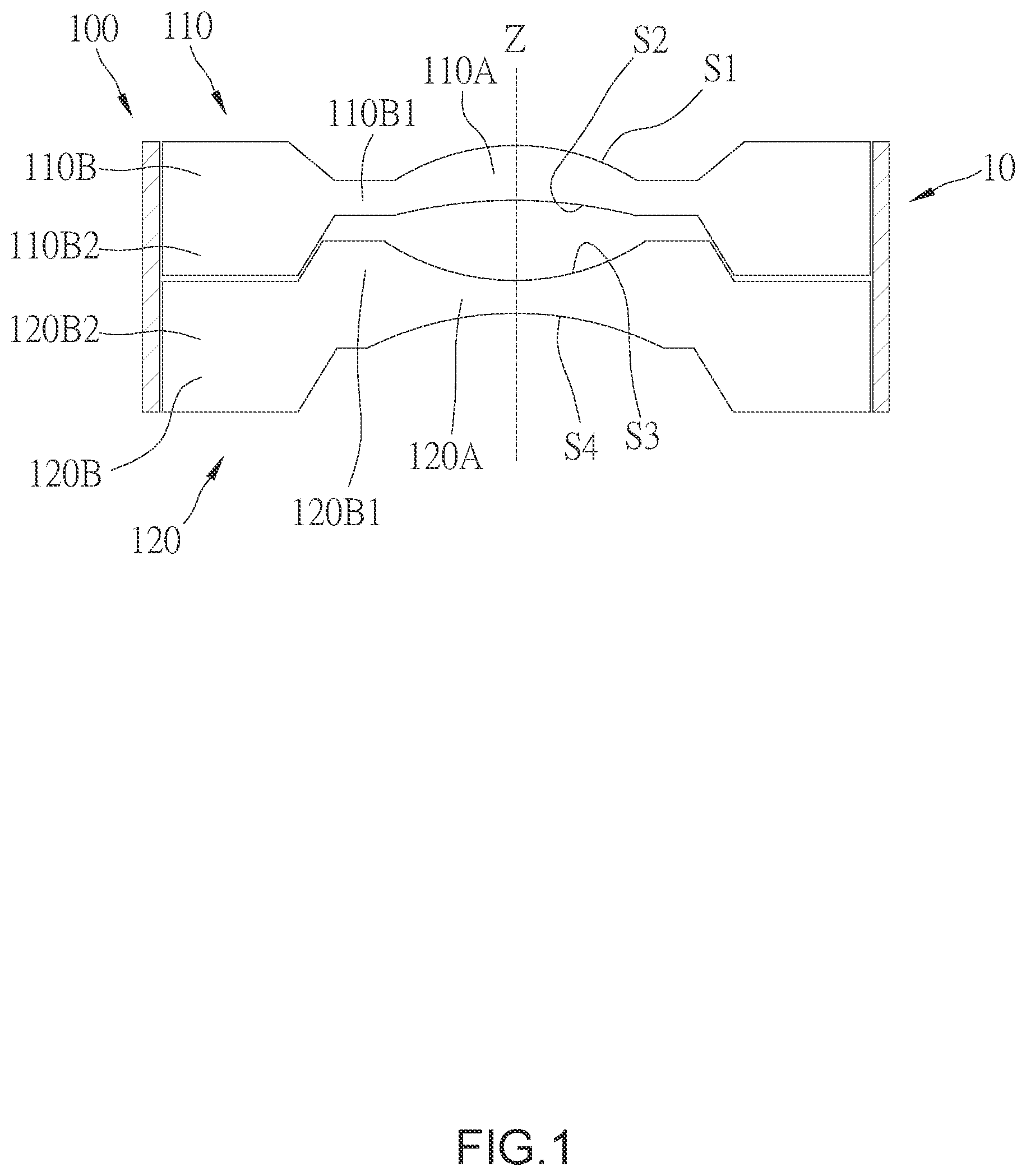
An optical lens 100 according to a first embodiment of the present invention is illustrated in to , which is adapted to be passed through by an image light and includes a first lens 110 , a second lens 120 , and a first shading layer 10 , wherein an optical axis Z of the image light sequentially passes through the first lens 110 and the second lens 120 .
The first lens 110 has a first optical valid area 110 A and a first optical invalid area 110 B. Referring to , the first optical valid area 110 A has a first upper optical surface S 1 and a first lower optical surface S 2 that face opposite directions, wherein the first optical valid area 110 A is a convex-concave type (i.e., the first upper optical surface S 1 is a convex surface and the first lower optical surface S 2 is a concave surface), and the first upper optical surface S 1 and the first lower optical surface S 2 are adapted to be passed through by the optical axis Z of the image light.
The first optical invalid area 110 B surrounds a periphery of the first optical valid area 110 A. Referring to , the first optical invalid area 110 B has a first connecting portion 110 B 1 and a first peripheral portion 110 B 2 , wherein a side of the first connecting portion 110 B 1 is connected to the first optical valid area 110 A, and another side thereof is connected to the first peripheral portion 110 B 2 , so that the first peripheral portion 110 B 2 is located on an outer periphery of the first lens 110 relative to the first optical valid area 110 A, and the first connecting portion 110 B 1 is connected between the first peripheral portion 110 B 2 and the first optical valid area 110 A.
More specifically, the first connecting portion 110 B 1 of the first lens 110 has a first upper connecting surface 111 and a first lower connecting surface 112 that face opposite directions, wherein the first upper connecting surface 111 is connected to a periphery of the first upper optical surface S 1 , and the first lower connecting surface 112 is connected to a periphery of the first lower optical surface S 2 ; the first peripheral portion 110 B 2 of the first lens 110 has a first upper peripheral surface 113 and a first lower peripheral surface 114 that face opposite directions. In the current embodiment, the first peripheral portion 110 B 2 extends from both the first upper peripheral surface 113 and the first lower peripheral surface 114 toward the first connecting portion 110 B 1 , and a width of the first peripheral portion 110 B 2 decreases gradually from both the first upper peripheral surface 113 and the first lower peripheral surface 114 toward the first connecting portion 110 B 1 ; the first peripheral portion 110 B 2 has a first abutting inclined surface 115 and a third abutting inclined surface 116 , wherein the first abutting inclined surface 115 is connected between the first lower peripheral surface 114 and the first lower connecting surface 112 in an inclined way, and the third abutting inclined surface 116 is connected between the first upper peripheral surface 113 and the first upper connecting surface 111 in an inclined way. Referring to , the first lower optical surface S 2 , the first lower connecting surface 112 , and the first lower peripheral surface 114 of the first lens 110 respectively face the second lens 120 .
The second lens 120 has a second optical valid area 120 A and a second optical invalid area 120 B, wherein the second optical valid area 120 A has a second upper optical surface S 3 and a second lower optical surface S 4 that face opposite directions. The second optical valid area 120 A is a biconcave type (i.e., the second upper optical surface S 3 is a concave surface and the second lower optical surface S 4 is a concave surface). The second upper optical surface S 3 and the second lower optical surface S 4 are adapted to be passed through by the optical axis Z of the image light.
The second optical invalid area 120 B surrounds a periphery of the second optical valid area 120 A and has a second connecting portion 120 B 1 and a second peripheral portion 120 B 2 , wherein a side of the second connecting portion 120 B 1 is connected to the second optical valid area 120 A, and another side of the second connecting portion 120 B 1 is connected to the second peripheral portion 120 B 2 , so that the second peripheral portion 120 B 2 is located on an outer periphery of the second lens 120 relative to the second optical valid area 120 A, and the second connecting portion 120 B 1 is connected between the second peripheral portion 120 B 2 and the second optical valid area 120 A.
More specifically, the second connecting portion 120 B 1 of the second lens 120 has a second upper connecting surface 121 and a second lower connecting surface 122 that face opposite directions, wherein the second upper connecting surface 121 is connected to a periphery of the second upper optical surface S 3 , and the second lower connecting surface 122 is connected to a periphery of the second lower optical surface S 4 ; the second peripheral portion 120 B 2 of the second lens 120 has a second upper peripheral surface 123 and a second lower peripheral surface 124 that face opposite directions. In the current embodiment, the second peripheral portion 120 B 2 extends from both the second upper peripheral surface 123 and the second lower peripheral surface 124 toward the first lens 110 to be connected to the second connecting portion 120 B 1 ; the second peripheral portion 120 B 2 has a second abutting inclined surface 125 and a fourth abutting inclined surface 126 , wherein the second abutting inclined surface 125 is connected between the second upper peripheral surface 123 and the second upper connecting surface 121 in an inclined way, and the fourth abutting inclined surface 126 is connected between the second lower peripheral surface 124 and the second lower connecting surface 122 in an inclined way.
The first peripheral portion 110 B 2 of the first lens 110 is disposed on the second peripheral portion 120 B 2 of the second lens 120 . More specifically, the first abutting inclined surface 115 of the first peripheral portion 110 B 2 is abutted against the second abutting inclined surface 125 of the second peripheral portion 120 B 2 , at that time, a peripheral gap G 1 is formed between the first lower peripheral surface 114 of the first peripheral portion 110 B 2 and the first upper peripheral surface 113 of the second peripheral portion 120 B 2 , and a connection gap P 1 is formed between the first lower connecting surface 112 of the first connecting portion 110 B 1 and the second upper connecting surface 121 of the second connecting portion 120 B 1 , and the second optical valid area 120 A of the second lens 120 faces the first optical valid area 110 A of the first lens 110 , allowing the optical axis Z of the image light sequentially passes through the first optical valid area 110 A and the second optical valid area 120 A.
The first shading layer 10 is made of an opaque material and is disposed on a peripheral edge of the first lens 110 and a peripheral edge of the second lens 120 . In the current embodiment, the first shading layer 10 is attached to both a side peripheral surface of the first peripheral portion 110 B 2 of the first lens 110 and a side peripheral surface of the second peripheral portion 120 B 2 of the second lens 120 (i.e., the first shading layer 10 surrounds an outer peripheral surface of the first optical invalid area 110 B and an outer peripheral surface of the second optical invalid area 120 B, wherein the opaque material of the first shading layer 10 includes a group selected from ceramics, metals, metal oxides, polyurethanes, epoxies, alkyds, polyester paints, and opaque adhesives; the metals includes pure metals such as aluminum (Al), copper (Cu), molybdenum (Mo), etc., and alloys, such as nickel chromium (NiCr), nickel aluminum (NiAl), aluminum bronze (CuAl), etc.; the metal oxides includes Aluminum oxide (Al 2 O 3 ), chromium oxide (Cr 2 O 3 ), zirconia (ZrO 2 ), titanium oxide (TiO 2 ), etc.
In other embodiments, the first shading layer 10 could be disposed on either the side peripheral surface of the first peripheral portion 110 B 2 of the first lens 110 or the side peripheral surface of the second peripheral portion 120 B 2 of the second lens 120 , or on both the side peripheral surface of the first peripheral portion 110 B 2 of the first lens 110 and the side peripheral surface of the second peripheral portion 120 B 2 of the second lens 120 to meet various requirements, wherein the first shading layer 10 correspondingly surrounds a periphery of the first optical invalid area 110 B or/and a periphery of the second optical invalid area 120 B, which could also achieve the effect of blocking non-imaging light from entering the optical valid areas.
Additionally, the first shading layer 10 could be ink, paint, or sheet, wherein if the first shading layer 10 is ink, the first shading layer 10 is formed on the side peripheral surface of the first peripheral portion 110 B 2 of the first lens 110 and the side peripheral surface of the second peripheral portion 120 B 2 of the second lens 120 by screen printing; if the first shading layer 10 is a paint, the first shading layer 10 is formed on the first peripheral portion 110 B 2 of the first lens 110 and the second peripheral portion 120 B 2 of the second lens 120 by coating; if the first shading layer 10 is a sheet, the first shading layer 10 is formed by attaching the sheet to the first peripheral portion 110 B 2 of the first lens 110 and the second peripheral portion 120 B 2 of the second lens 120 . However, the way of setting the first shading layer 10 is not limited by the aforementioned design, as long as the first shading layer 10 could be disposed on the first peripheral portion 110 B 2 of the first lens 110 and the second peripheral portion 120 B 2 of the second lens 120 .
In summary, since the first shading layer 10 of the optical lens 100 has the function of blocking light and is disposed on the side peripheral surface of the first peripheral portion 110 B 2 of the first lens 110 and the side peripheral surface of the second peripheral portion 120 B 2 of the second lens 120 , the first shading layer 10 could effectively block the non-imaging light while practical use, so that the non-imaging light could not pass through the first optical invalid area 110 B and the second optical invalid area 120 B through the side peripheral surface of the first lens 110 or the side peripheral surface of the second lens 120 , thereby enhancing the imaging quality, reducing the number of light-shielding parts, reducing the cost of parts, and shortening the assembling time, achieving the miniaturization of the optical lens 100 and improving the optical imaging quality.
Referring to , the optical lens 100 according to the first embodiment further includes a second shading layer 11 for increasing an shading area of the optical lens 100 .
The second shading layer 11 is made of an opaque material and is disposed on the first optical invalid area 110 B of the first lens 110 . In the current embodiment, the second shading layer 11 is attached to the first upper connecting surface 111 of the first connecting portion 110 B 1 , the first upper peripheral surface 113 of the first peripheral portion 110 B 2 , and the third abutting inclined surface 116 (i.e., the second shading layer 11 surrounds a periphery of the first upper optical surface S 1 of the first optical valid area 110 A), and the first shading layer 10 and the second shading layer 11 are made of different materials, wherein the opaque material of the second shading layer 11 is selected from ceramics, metals, metal oxides, polyurethanes, epoxies, alkyds, polyester paints, opaque adhesives, and a combination thereof; the metals includes pure metals such as aluminum (Al), copper (Cu), molybdenum (Mo), etc., and alloys, such as nickel chromium (NiCr), nickel aluminum (NiAl), aluminum bronze (CuAl), etc.; the metal oxides includes Aluminum oxide (Al 2 O 3 ), chromium oxide (Cr 2 O 3 ), zirconia (ZrO 2 ), titanium oxide (TiO 2 ), etc. In other embodiments, the first shading layer 10 and the second shading layer 11 could be made of the same material to meet various requirements.
More specifically, the second shading layer 11 could be ink, paint, or sheet, wherein the way of setting the second shading layer 11 is the same as that of the first shading layer 10 (e.g. by screen printing, coating, and attaching). For instance, if the second shading layer 11 is ink, the second shading layer 11 is formed on the first optical invalid area 110 B by screen printing; if the second shading layer 11 is a paint, the second shading layer 11 is formed on the first optical invalid area 110 B by coating; if the second shading layer 11 is a sheet, the second shading layer 11 is formed by attaching the sheet to the first optical invalid area 110 B. However, the way of setting the second shading layer 11 is not limited by the aforementioned design.
In other embodiments, the first shading layer 10 and the second shading layer 11 could be made of the same material to meet various requirements; the second shading layer 11 could be disposed on the first upper connecting surface 111 of the first connecting portion 110 B 1 , the first upper peripheral surface 113 of the first peripheral portion 110 B 2 , or both the first upper connecting surface 111 of the first connecting portion 110 B 1 and the first upper peripheral surface 113 of the first peripheral portion 110 B 2 ; alternatively, the second shading layer 11 could be omitted.
With the second shading layer 11 , the optical lens 100 could further block the non-imaging light from entering the first optical invalid area 110 B through the first connecting portion 110 B 1 and first peripheral portion 110 B 2 of the first lens 110 , and could concentrate the image light into the first optical valid area 110 A, which further improves the imaging quality of the optical lens 100 and further saves the cost of shading parts.
Referring to , the optical lens 100 according to the first embodiment further includes a third shading layer 12 for enhancing the shading effect.
The third shading layer 12 is made of an opaque material and is disposed between the first lens 110 and the second lens 120 . In the current embodiment, the third shading layer 12 is located in the peripheral gap G 1 formed between the first peripheral portion 110 B 2 and the second peripheral portion 120 B 2 , and gets in contact with the first lower peripheral surface 114 and the second upper peripheral surface 123 , wherein the first shading layer 10 and the third shading layer 12 are made of different materials. The opaque material of the third shading layer 12 is selected from ceramics, metals, metal oxides, polyurethanes, epoxies, alkyds, polyester paints, opaque adhesives, and a combination thereof; the metals include pure metals such as aluminum (Al), copper (Cu), molybdenum (Mo), etc., and alloys, such as nickel chromium (NiCr), nickel aluminum (NiAl), aluminum bronze (CuAl), etc.; the metal oxides includes Aluminum oxide (Al 2 O 3 ), chromium oxide (Cr 2 O 3 ), zirconia (ZrO 2 ), titanium oxide (TiO 2 ), etc.
Additionally, the third shading layer 12 could be ink, paint, or sheet, wherein the way of setting the third shading layer 12 in the peripheral gap G 1 is the same as that of the first shading layer 10 . However, the way of setting the third shading layer 12 is not limited by the aforementioned design, as long as the third shading layer 12 could be formed in the peripheral gap G 1 . In other embodiments, the first shading layer 10 , the second shading layer 11 , and the third shading layer 12 could be made of the same material and be set in the same way to meet various requirements; alternatively, the third shading layer 12 could be omitted.
With the third shading layer 12 , the optical lens 100 could further block the non-imaging light from entering the second peripheral portion 120 B 2 of the second lens 120 through the first peripheral portion 110 B 2 of the first lens 110 , thereby reducing the interference of the non-imaging light to the second lens 120 , improving the imaging effect of the optical lens 100 .
Referring to , the optical lens 100 according to the first embodiment further includes a fourth shading layer 13 for enhancing the shading effect.
The fourth shading layer 13 is made of an opaque material and is disposed between the first lens 110 and the second lens 120 . In the current embodiment, the fourth shading layer 13 is located in the connection gap P 1 formed between the first lower connecting surface 112 of the first connecting portion 110 B 1 and the second upper connecting surface 121 of the second connecting portion 120 B 1 , and is attached to the first lower connecting surface 112 and the second upper connecting surface 121 , wherein the first shading layer 10 and the fourth shading layer 13 are made of different materials. The opaque material of the fourth shading layer 13 is selected from ceramics, metals, metal oxides, polyurethanes, epoxies, alkyds, polyester paints, opaque adhesives, and a combination thereof; the metals include pure metals such as aluminum (Al), copper (Cu), molybdenum (Mo), etc., and alloys, such as nickel chromium (NiCr), nickel aluminum (NiAl), aluminum bronze (CuAl), etc.; the metal oxides includes Aluminum oxide (Al 2 O 3 ), chromium oxide (Cr 2 O 3 ), zirconia (ZrO 2 ), titanium oxide (TiO 2 ), etc.
Additionally, the fourth shading layer 13 could be ink, paint, or sheet, wherein the way of setting the fourth shading layer 13 in the connection gap P 1 is the same as that of the first shading layer 10 . However, the way of setting the fourth shading layer 13 is not limited by the aforementioned design, as long as the fourth shading layer 13 could be formed in the connection gap P 1 . In other embodiments, the first shading layer 10 , the second shading layer 11 , the third shading layer 12 , and the fourth shading layer 13 could be made of the same material and be set in the same way to meet various requirements; alternatively, the fourth shading layer 13 could be omitted.
In the current embodiment, the second shading layer 11 of the optical lens 100 is separated into a peripheral section 11 a and a connecting section 11 b , wherein the peripheral section 11 a is disposed on the first upper peripheral surface 113 of the first peripheral portion 110 B 2 and a part of the third abutting inclined surface 116 , and the connecting section 11 b is disposed on the first upper connecting surface 111 of the first connecting portion 110 B 1 ; the peripheral section 11 a does not get in contact with the connecting section 11 b , not affecting the imaging quality of the optical lens 100 . In other embodiments, the peripheral section 11 a could get in contact with the connecting section 11 b , avoiding the leakage of ineffective light.
With the fourth shading layer 13 , the optical lens 100 could strengthen the blocking of the non-imaging light from the first connecting portion 110 B 1 of the first lens 110 into the second connecting portion 120 B 1 of the second lens 120 , further reducing the interference of the non-imaging light to the second lens 120 , improving the imaging effect of the optical lens 100 . Without compromising the imaging quality of the optical lens 100 , the second shading layer 11 could be designed in segments.
An optical lens 200 according to a second embodiment of the present invention is illustrated in and and includes a first lens 210 and a second lens 220 .
The first lens 210 has a first optical valid area 210 A and a first optical invalid area 210 B. Referring to , the first optical valid area 210 A has a first upper optical surface S 1 and a first lower optical surface S 2 that face opposite directions, wherein the first optical valid area 210 A is a convex-concave type (i.e., the first upper optical surface S 1 is a convex surface and the first lower optical surface S 2 is a concave surface), and the first upper optical surface S 1 and the first lower optical surface S 2 are adapted to be passed through by the optical axis Z of the image light.
The first optical invalid area 210 B surrounds a periphery of the first optical valid area 210 A. Referring to , the first optical invalid area 210 B has a first connecting portion 210 B 1 and a first peripheral portion 210 B 2 , wherein a side of the first connecting portion 210 B 1 is connected to the first optical valid area 210 A, and another side of the first connecting portion 210 B 1 is connected to the first peripheral portion 210 B 2 , so that the first peripheral portion 210 B 2 is located on an outer periphery of the first lens 210 relative to the first optical valid area 210 A, and the first connecting portion 210 B 1 is connected between the first peripheral portion 210 B 2 and the first optical valid area 210 A.
In the current embodiment, at least a part of the first peripheral portion 210 B 2 is made of an opaque material, wherein the opaque material could be opaque plastic materials, or could be formed by modifying light-transmitting materials through laser modification. In the current embodiment, a part of the first peripheral portion 210 B 2 is made of opaque plastic materials, wherein the first peripheral portion 210 B 2 has a first upper peripheral surface 213 and a first lower peripheral surface 214 that face opposite directions; the part of the first peripheral portion 210 B 2 that is opaque is an area between the first upper peripheral surface 213 and the first lower peripheral surface 214 .
Additionally, the first connecting portion 210 B 1 of the first lens 210 has a first upper connecting surface 211 and a first lower connecting surface 212 that face opposite directions, wherein the first upper connecting surface 211 is connected to a periphery of the first upper optical surface S 1 , and the first lower connecting surface 212 is connected to a periphery of the first lower optical surface S 2 ; the first peripheral portion 210 B 2 extends from both the first upper peripheral surface 213 and the first lower peripheral surface 214 toward the first connecting portion 210 B 1 , and a width of the first peripheral portion 210 B 2 decreases gradually from both the first upper peripheral surface 213 and the first lower peripheral surface 214 toward the first connecting portion 210 B 1 ; the first peripheral portion 210 B 2 has a first abutting inclined surface 215 and a third abutting inclined surface 216 , wherein the first abutting inclined surface 215 is connected between the first lower peripheral surface 214 and the first lower connecting surface 212 in an inclined way, and the third abutting inclined surface 216 is connected between the first upper peripheral surface 213 and the first upper connecting surface 211 in an inclined way.
The second lens 220 has a second optical valid area 220 A and a second optical invalid area 220 B, wherein the second optical valid area 220 A has a second upper optical surface S 3 and a second lower optical surface S 4 that face opposite directions. The second optical valid area 220 A is a biconcave type (i.e., the second upper optical surface S 3 is a concave surface and the second lower optical surface S 4 is a concave surface). The second upper optical surface S 3 and the second lower optical surface S 4 are adapted to be passed through by the optical axis Z of the image light.
The second optical invalid area 220 B surrounds a periphery of the second optical valid area 220 A and has a second connecting portion 220 B 1 and a second peripheral portion 220 B 2 , wherein a side of the second connecting portion 220 B 1 is connected to the second optical valid area 220 A, and another side of the second connecting portion 220 B 1 is connected to the second peripheral portion 220 B 2 , so that the second peripheral portion 220 B 2 is located on an outer periphery of the second lens 220 relative to the second optical valid area 220 A, and the second connecting portion 220 B 1 is connected between the second peripheral portion 220 B 2 and the second optical valid area 220 A.
In the current embodiment, at least a part of the second peripheral portion 220 B 2 is made of an opaque material, wherein the opaque material could be opaque plastic materials, or could be formed by modifying light-transmitting materials through laser modification. In the current embodiment, a part of the second peripheral portion 220 B 2 is made of opaque plastic materials, wherein the second peripheral portion 220 B 2 has a second upper peripheral surface 223 and a second lower peripheral surface 224 that face opposite directions; the part of the second peripheral portion 220 B 2 that is opaque is an area between the second upper peripheral surface 223 and the second lower peripheral surface 224 .
Additionally, the second connecting portion 220 B 1 of the second lens 220 has a second upper connecting surface 221 and a second lower connecting surface 222 that face opposite directions, wherein the second upper connecting surface 211 is connected to a periphery of the second upper optical surface S 3 , and the second lower connecting surface 222 is connected to a periphery of the second lower optical surface S 4 ; the second peripheral portion 220 B 2 tilts upward from both the second upper peripheral surface 223 and the second lower peripheral surface 224 toward the first lens 210 to be connected to the second connecting portion 220 B 1 ; the second peripheral portion 220 B 2 has a second abutting inclined surface 225 and a fourth abutting inclined surface 226 , wherein the second abutting inclined surface 225 is connected between the second upper peripheral surface 223 and the second upper connecting surface 221 in an inclined way, and the fourth abutting inclined surface 226 is connected between the second lower peripheral surface 224 and the second lower connecting surface 222 in an inclined way.
In this way, since some areas of the first peripheral portion 210 B 2 of the first lens 210 and some areas of the second peripheral portion 220 B 2 of the second lens 220 are opaque, both the first optical invalid area 210 B of the first lens 210 and the second optical invalid area 220 B of the second lens 220 could block light, effectively blocking non-imaging light from the side peripheral surface of the first peripheral portion 210 B 2 and the side peripheral surface of the second peripheral portion 220 B 2 into the first lens 210 and the second lens 220 as well, improving the imaging effect. Additionally, the optical lens 200 of the second embodiment could save more light-shielding materials than that of the first embodiment, which could reduce the lens processing cost of the optical lens 200 .
Referring to , the optical lens 200 of the current embodiment further includes a first shading layer 20 and a second shading layer 21 .
The first shading layer 20 is made of an opaque material, wherein the first shading layer 20 is disposed on the side peripheral surface of the first peripheral portion 210 B 2 , the side peripheral surface of the second peripheral portion 220 B 2 , or both the side peripheral surface of the first peripheral portion 210 B 2 and the side peripheral surface of the second peripheral portion 220 B 2 , and correspondingly surrounds the first optical invalid area 210 B or/and the second optical invalid area 220 B. In the current embodiment, the first shading layer 20 surrounds the first peripheral portion 210 B 2 and the second peripheral portion 220 B 2 and forms an opaque surface on the both the side peripheral surface of the first peripheral portion 210 B 2 and the side peripheral surface of the second peripheral portion 220 B 2 through laser modification.
The second shading layer 21 is made of an opaque material and is disposed on the first upper connecting surface 211 of the first connecting portion 210 B 1 , the first upper peripheral surface 213 of the first peripheral portion 210 B 2 , and the third abutting inclined surface 216 . In the current embodiment, the second shading layer 21 forms an opaque surface on the side peripheral surface of the first peripheral portion 210 B 2 and the side peripheral surface of the first connecting portion 210 B 1 through laser modification.
In other embodiments, the second shading layer 21 could be disposed on the first upper connecting surface 211 of the first connecting portion 210 B 1 , the first upper peripheral surface 213 of the first peripheral portion 210 B 2 , or on both the first upper connecting surface 211 of the first connecting portion 210 B 1 and the first upper peripheral surface 213 of the first peripheral portion 210 B 2 .
With the first shading layer 20 and the second shading layer 21 , the optical lens 200 could strengthen the blocking of the non-imaging light from the peripheral surface of the first lens 210 and the peripheral surface of the second lens 220 into the first peripheral portion 210 B 2 of the first lens 210 and the second peripheral portion 220 B 2 of the second lens 220 , and could strengthen the blocking of the non-imaging light from a side of the first peripheral portion 210 B 2 and a side of the first connecting portion 210 B 1 of the first lens 210 into the first optical invalid area 210 B, further improving the imaging effect of the optical lens 200 .
An optical lens 300 according to a third embodiment of the present invention is illustrated in to and includes a first lens 310 , a second lens 320 , a first shading layer 30 , a second shading layer 31 , a third shading layer 32 , a fourth shading layer 33 , and an image light sensing module 330 , wherein the first lens 310 and the second lens 320 of the current embodiment has almost the same structure as that of the first embodiment. In other words, the first lens 310 of the current embodiment has a first optical valid area 310 A and a first optical invalid area 310 B, wherein the first optical valid area 310 A has a first upper optical surface S 1 and a first lower optical surface S 2 , and the first optical invalid area 310 B has a first connecting portion 310 B 1 and a first peripheral portion 310 B 2 . Similarly, the second lens 320 has a second optical valid area 320 A and a second optical invalid area 320 B, wherein the second optical valid area 320 A has a second upper optical surface S 3 and a second lower optical surface S 4 , and the second optical invalid area 320 B has a second connecting portion 320 B 1 and a second peripheral portion 320 B 2 . Referring to and , the first shading layer 30 , the second shading layer 31 , the third shading layer 32 , and the fourth shading layer 33 of the current embodiment are disposed and arranged similarly to the first shading layer 10 , the second shading layer 11 , the third shading layer 12 , and the fourth shading layer 13 of the first embodiment shown in , thus we are not going to describe in details herein.
The difference between the optical lens 300 of the current embodiment and that of the first embodiment is that the optical lens 300 further includes the image light sensing module 330 , and the structure of the second peripheral portion 320 B 2 of the second lens 320 of the current embodiment is slightly different from the second lens 120 of the first embodiment.
More specifically, the image light sensing module 330 includes an image sensing member 331 and a substrate 332 , wherein the image sensing member 331 is adapted to receive the image light; the second optical valid area 320 A of the second lens 320 faces the image sensing member 331 ; the substrate 332 is adapted to dispose the second peripheral portion 320 B 2 of the second lens 320 , wherein the second peripheral portion 320 B 2 has an extending section 325 . Referring to , the extending section 325 extends downward from the second lower peripheral surface 324 , wherein the extending section 325 surrounds and forms an inner space S therein. The first shading layer 30 surrounds the side peripheral surface of the second peripheral portion 320 B 2 of the second lens 320 (including the side peripheral surface of the extending section 325 ). In practice, during a process of assembling the second lens 320 and the image light sensing module 330 , the image sensing member 331 is disposed on the substrate 332 , and then the extending section 325 of the second peripheral portion 320 B 2 is disposed on the substrate 332 , thereby the image sensing member 331 is located in the inner space S, and the second optical valid area 320 A is located above the image sensing member 331 .
Referring to , the image light sensing module 330 of the current embodiment could further include a spacer 333 disposed on the substrate 332 and located around the image sensing member 331 , wherein the extending section 325 of the second peripheral portion 320 B 2 of the second lens 320 is disposed on the spacer 333 , thereby reducing a length of the extending section 325 of the second peripheral portion 320 B 2 (i.e., reducing a thickness of the second lens 320 ).
Referring to , the structures of the spacer 333 and the first shading layer 30 of the current embodiment could be changed to meet different requirements.
More specifically, the first shading layer 30 is disposed on the side peripheral surface of the first peripheral portion 310 B 2 of the first lens 310 , and the spacer 333 has a light-shielding sheet 334 and a restricting block 335 . Referring to , the light-shielding sheet 334 extends upward from a side of the spacer 333 , and the restricting block 335 protrudes from another side of the spacer 333 , wherein a recess 336 is formed between the light-shielding sheet 334 and the restricting block 335 . In practice, during a process of assembling the second lens 320 and the image light sensing module 330 , the extending section 325 of the second peripheral portion 320 B 2 of the second lens 320 is positioned in the recess 336 of the spacer 333 , and the light-shielding sheet 334 surrounds the side peripheral surface of the second peripheral portion 320 B 2 of the second lens 320 . In this way, the first shading layer 30 of the current embodiment surrounds a periphery of the first peripheral portion 310 B 2 of the first lens 310 , and the light-shielding sheet 334 of the current embodiment surrounds a periphery of the second peripheral portion 320 B 2 of the second lens 320 , wherein since the first shading layer 30 and the light-shielding sheet 334 have the function of blocking light, the non-imaging light could not pass through the first shading layer 30 and the light-shielding sheet 334 to enter the first peripheral portion 310 B 2 and the second peripheral portion 320 B 2 , which could also provide the light-blocking effect.
In other embodiments, the first shading layer 30 could be disposed on the side peripheral surface of the second peripheral portion 320 B 2 of the second lens 320 , and the light-shielding sheet 334 could be further disposed on the first peripheral portion 310 B 2 of the first lens 310 for blocking light, as long as the first shading layer 30 is disposed on at least one of the lenses; alternatively, the first shading layer 30 could be omitted, and a part of the peripheral portion of at least one of the lenses could be made of an opaque material, allowing the optical invalid area of at least one of the lenses to provide light-blocking effect to block the non-imaging light from the side peripheral surface of the peripheral portion into at least one of the lenses, further saving the light-shielding materials.
An optical lens 400 according to a fourth embodiment of the present invention is illustrated in and and includes a first lens 410 , a second lens 420 , a third lens 430 , a first shading layer 40 , a second shading layer 41 , two third shading layers 42 , two fourth shading layers 43 , an image light sensing module 440 , and a filter 450 .
The first lens 410 , the second lens 420 , and the image light sensing module 440 of the optical lens 400 of the current embodiment have almost the same structure as the first lens 310 , the second lens 320 , and the image light sensing module 330 of the optical lens 300 of the third embodiment. In other words, the first lens 410 has a first optical valid area 410 A and a first optical invalid area 410 B, wherein the first optical valid area 410 A has a first upper optical surface S 1 and a first lower optical surface S 2 , and the first optical invalid area 410 B has a first connecting portion 410 B 1 and a first peripheral portion 410 B 2 . Similarly, the second lens 420 has a second optical valid area 420 A and a second optical invalid area 420 B, wherein the second optical valid area 420 A has a second upper optical surface S 3 and a second lower optical surface S 4 , and the second optical invalid area 420 B has a second connecting portion 420 B 1 and a second peripheral portion 420 B 2 ; the image light sensing module 440 at least has an image light sensing member 441 and a substrate 442 , wherein the image light sensing module 440 could include a spacer 443 (shown in ); the second shading layer 41 of the current embodiment is disposed and arranged similarly to the second shading layer 31 of the third embodiment, thus we are not going to describe in details herein.
The difference between the optical lens 400 of the current embodiment and that of the third embodiment is that the optical lens 400 further includes the third lens 430 and the filter 450 , and the arrangements of the first shading layer 40 , the two third shading layers 42 , and the two fourth shading layers 43 are slightly different.
The third lens 430 has a third optical valid area 430 A and a third optical invalid area 430 B, wherein the third optical valid area 430 A has a third upper optical surface S 5 and a third lower optical surface S 6 that face opposite directions. The third optical valid area 430 A is a concave-convex type (i.e., the third upper optical surface S 5 is a concave surface, the third lower optical surface S 6 is a convex surface), and the third upper optical surface S 5 and the third lower optical surface S 6 are adapted to be passed through by the optical axis Z of the image light.
The third optical invalid area 430 B surrounds a periphery of the third optical valid area 430 A and has a third connecting portion 430 B 1 and a third peripheral portion 430 B 2 , wherein a side of the third connecting portion 430 B 1 is connected to the third optical valid area 430 A, and another side of the third connecting portion 430 B 1 is connected to the third peripheral portion 430 B 2 , so that the third peripheral portion 430 B 2 could be located on an outer periphery of the third lens 430 relative to the third optical valid area 430 A, and the third connecting portion 430 B 1 is connected between the third peripheral portion 430 B 2 and the third optical valid area 430 A.
Referring to , the third connecting portion 430 B 1 has a third upper connecting surface 431 and a third lower connecting surface 432 that face opposite directions, wherein the third upper connecting surface 431 is connected to a periphery of the third upper optical surface S 5 , and the third lower connecting surface 432 is connected to a periphery of the third lower optical surface S 6 ; the third peripheral portion 430 B 2 has a third upper peripheral surface 433 and a third lower peripheral surface 434 that face opposite directions, wherein the third peripheral portion 430 B 2 tilts upward from both the third upper peripheral surface 433 and the third lower peripheral surface 434 toward the second lens 420 to be connected to the third connecting portion 430 B 1 .
Referring to , the second peripheral portion 420 B 2 of the second lens 420 is disposed on the third peripheral portion 430 B 2 of the third lens 430 , wherein a peripheral gap G 2 is formed between the second peripheral portion 420 B 2 and the third peripheral portion 430 B 2 , and a connection gap P 2 is formed between the second connecting portion 420 B 1 and the third connecting portion 430 B 1 ; the second optical valid area 420 A of the second lens 420 faces the third optical valid area 430 A of the third lens 430 , so that the optical axis Z of the image light could pass through the second optical valid area 420 A and the third optical valid area 430 A.
Additionally, the third peripheral portion 430 B 2 of the third lens 430 has an extending section 435 extending downward from the third lower peripheral surface 434 (as shown in and ), wherein the extending section 435 is disposed above the substrate 442 of the image light sensing module 440 , the image sensing member 441 is located on the substrate 442 , and the third optical valid area 430 A is located above the image sensing member 441 . As the way of setting the third lens 430 and the image light sensing module 440 of the current embodiment is almost the same as the way of setting the second lens 320 and the image light sensing module 330 of the third embodiment, thus we are not going to describe in details herein.
Moreover, the filter 450 is disposed between the third lens 430 and the image sensing member 441 , and does not affect a focal length of the optical lens 400 of the current embodiment. Referring to , the filter 450 is connected to the third lower peripheral surface 434 of the third lens 430 and is located above the image sensing member 441 . However, the arrangement of the filter 450 is not limited by the aforementioned design. Referring to , the filter 450 abuts against the restricting block 444 of the spacer 443 and is located above the image sensing member 441 .
Referring to and , in the current embodiment, the first shading layer 40 is disposed on the side peripheral surface of the first peripheral portion 410 B 2 of the first lens 410 , the side peripheral surface of the second peripheral portion 420 B 2 of the second lens 420 , and the side peripheral surface of the third peripheral portion 430 B 2 of the third lens 430 , wherein the third lens 430 of the first shading layer 40 surrounds the side peripheral surface of the extending section 435 of the third peripheral portion 430 B 2 ; the two third shading layers 42 are respectively disposed in the peripheral gap G 1 formed between the first peripheral portion 410 B 2 and the second peripheral portion 420 B 2 and the peripheral gap G 2 formed between the second peripheral portion 420 B 2 and the third peripheral portion 430 B 2 ; the two fourth shading layers 43 are respectively disposed in the connection gap P 1 formed between the first connecting portion 410 B 1 and the second connecting portion 420 B 1 and the connection gap P 2 formed between the second connecting portion 420 B 1 and the third connecting portion 430 B 1 , wherein the way of setting the first shading layer 40 , the second shading layer 41 , each of the third shading layers 42 , and each of the fourth shading layers 43 is the same as that of the first embodiment (e.g. by screen printing, coating, and attaching). In this way, the arrangement of the shading layers of the current embodiment could be changed depending on the number of lenses to meet different requirements, allowing the optical lens 400 to have the function of blocking light.
An optical lens 500 according to a fifth embodiment of the present invention is illustrated in and and includes a first lens 510 , a second lens 520 , a third lens 530 , a fourth lens 540 , a first shading layer 50 , a second shading layer 51 , three third shading layers 52 , three fourth shading layers 53 , an image light sensing module 550 , and a filter 560 , wherein the first lens 510 , the second lens 520 , the third lens 530 , and the image light sensing module 550 of the current embodiment has almost the same structure as the first lens 410 , the second lens 420 , the third lens 430 , and the image light sensing module 440 of the fourth embodiment.
In other words, the first lens 510 of the current embodiment has a first optical valid area 510 A and a first optical invalid area 510 B, wherein the first optical valid area 510 A has a first upper optical surface S 1 and a first lower optical surface S 2 and the first optical invalid area 510 B has a first connecting portion 510 B 1 and a first peripheral portion 510 B 2 ; the second lens 520 has a second optical valid area 520 A and a second optical invalid area 520 B; the second optical valid area 520 A has a second upper optical surface S 3 and a second lower optical surface S 4 and the second optical invalid area 520 B has a second connecting portion 520 B 1 and a second peripheral portion 520 B 2 ; the third lens 530 has a third optical valid area 530 A and a third optical invalid area 530 B; the third optical valid area 530 A has a third upper optical surface S 5 and a third lower optical surface S 6 and the third optical invalid area 530 B has a third connecting portion 530 B 1 and a third peripheral portion 530 B 2 ; the image light sensing module 550 at least has an image light sensing member 551 and a substrate 552 ; the image light sensing module 550 could further include a spacer 553 (as shown in ); the second shading layer 51 of the current embodiment is disposed and arranged similarly to the second shading layer 41 of the fourth embodiment, thus we are not going to describe in details herein.
The difference between the optical lens 500 of the current embodiment and that of the fourth embodiment is that the optical lens 500 of the current embodiment further includes the fourth lens 540 , and the arrangements of the first shading layer 50 , the three third shading layers 52 , and the three fourth shading layers 53 are slightly different.
Referring to and , the fourth lens 540 has a fourth optical valid area 540 A and a fourth optical invalid area 540 B, wherein the fourth optical valid area 540 A has a fourth upper optical surface S 7 and a fourth lower optical surface S 8 that face opposite directions. The fourth optical valid area 540 A is a biconcave type (i.e., the fourth upper optical surface S 7 is a concave surface, and the fourth lower optical surface S 8 is a concave surface), wherein the fourth upper optical surface S 7 and the fourth lower optical surface S 8 are adapted to be passed through by the optical axis Z of the image light.
The fourth optical invalid area 540 B surrounds a periphery of the fourth optical valid area 540 A and has a fourth connecting portion 540 B 1 and a fourth peripheral portion 540 B 2 , wherein a side of the fourth connecting portion 540 B 1 is connected to the fourth optical valid area 540 A, and another side of the fourth connecting portion 540 B 1 is connected to the fourth peripheral portion 540 B 2 , so that the fourth peripheral portion 540 B 2 could be located on an outer periphery of the fourth lens 540 relative to the fourth optical valid area 540 A, and the fourth connecting portion 540 B 1 is connected between the fourth peripheral portion 540 B 2 and the fourth optical valid area 540 A.
Referring to , the fourth connecting portion 540 B 2 has a fourth upper connecting surface 541 and a fourth lower connecting surface 542 that face opposite directions, wherein the fourth upper connecting surface 541 is connected to a periphery of the fourth upper optical surface S 7 , and the fourth lower connecting surface 542 is connected to a periphery of the fourth lower optical surface S 8 ; the fourth peripheral portion 540 B 2 has a fourth upper peripheral surface 543 and a fourth lower peripheral surface 544 that face opposite directions, wherein the fourth peripheral portion 540 B 2 tilts upward from both the fourth upper peripheral surface 543 and the fourth lower peripheral surface 544 toward the third lens 530 to be connected to the fourth connecting portion 540 B 1 .
In the current embodiment, the third peripheral portion 530 B 2 of the third lens 530 is disposed on the fourth peripheral portion 540 B 2 of the fourth lens 540 , wherein a peripheral gap G 3 is formed between the third peripheral portion 530 B 2 and the fourth peripheral portion 540 B 2 , and a connection gap P 3 is formed between the third connecting portion 530 B 1 and the fourth connecting portion 540 B 1 ; the third optical valid area 530 A of the third lens 530 and the fourth optical valid area 540 A of the fourth lens 540 face each other, and the optical axis Z of the image light passes through the third optical valid area 530 A and the fourth optical valid area 540 A.
Additionally, the fourth peripheral portion 540 B 2 has an extending section 545 extending downward from the fourth lower peripheral surface 544 (as shown in and ), wherein the extending section 545 is disposed above the substrate 552 of the image light sensing module 550 , the image sensing member 551 is disposed on the substrate 552 , and the fourth optical valid area 540 A is located above the image sensing member 551 .
Referring to and , in the current embodiment, the first shading layer 50 is disposed on the side peripheral surface of the first peripheral portion 510 B 2 of the first lens 510 , the side peripheral surface of the second peripheral portion 520 B 2 of the second lens 520 , the side peripheral surface of the third peripheral portion 530 B 2 of the third lens 530 , and the side peripheral surface of the fourth peripheral portion 540 B 2 of the fourth lens 540 , wherein the first shading layer 50 further surrounds the side peripheral surface of the extending section 545 of the fourth peripheral portion 540 B 2 of the fourth lens 540 ; the three third shading layers 52 are respectively disposed in the three peripheral gaps G 1 , G 2 , G 3 , and the three fourth shading layers 53 are respectively disposed in the three connection gaps P 1 , P 2 , P 3 , wherein the way of setting the first shading layer 50 , the second shading layer 51 , each of the third shading layers 52 , and each of the fourth shading layers 53 is the same as that of the first embodiment (e.g. by screen printing, coating, and attaching). In this way, the arrangement of the shading layers of the current embodiment could be changed depending on the number of lenses to meet different requirements, allowing the optical lens 500 to have the function of blocking light.
An optical lens 600 according to a sixth embodiment of the present invention is illustrated in and and includes five lenses, a first shading layer 60 , a second shading layer 61 , four third shading layers 62 , four fourth shading layers 63 , an image light sensing module 650 , and a filter 660 , wherein the five lenses, in order along the optical axis Z, have a first lens 610 , two second lenses 620 , a third lens 630 , and a fourth lens 640 . The first lens 610 , the second lens 620 , the third lens 630 , the fourth lens 640 , and the image light sensing module 650 of the current embodiment has almost the same structure as the first lens 510 , the second lens 520 , the third lens 530 , the fourth lens 540 , and the image light sensing module 550 of the fifth embodiment; the first shading layer 60 to the fourth shading layer 63 of the current embodiment are disposed and arranged similarly to the first shading layer 50 to the fourth shading layer 53 of the fifth embodiment, thus we are not going to describe in details herein.
The difference between the optical lens 600 of the current embodiment and that of the fifth embodiment is that the optical lens 600 of the current embodiment includes the two second lenses 620 . More specifically, the two second lenses 620 are disposed between the first lens 610 and the third lens 630 , and the two second lenses 620 are both biconcave type, wherein the way of setting the first shading layer 60 , the second shading layer 61 , each of the third shading layers 62 , and each of the fourth shading layers 63 is the same as that of the first embodiment (e.g. by screen printing, coating, and attaching). In this way, the arrangement of the shading layers of the current embodiment could be changed depending on the number of lenses to meet different requirements, allowing the optical lens 600 to have the function of blocking light.
An optical lens 700 according to a seventh embodiment of the present invention is illustrated in and and includes ten lenses, a first shading layer 70 , a second shading layer 71 , a plurality of third shading layers 72 , a plurality of fourth shading layer 73 , an image light sensing module 810 , and at least one filter 820 , wherein the ten lenses, in order along the optical axis Z, have a first lens 710 , a second lens 720 , a third lens 730 , a fourth lens 740 , a fifth lens 750 , a sixth lens 760 , a seventh lens 770 , an eighth lens 780 , a ninth lens 790 , and a tenth lens 800 .
The first lens 710 has a first optical valid area 710 A and a first optical invalid area 710 B. Referring to and , the first optical valid area 710 A has a first upper optical surface S 1 and a first lower optical surface S 2 , wherein the first optical valid area 710 A is a convex-concave type (i.e., the first upper optical surface S 1 is a convex surface and the first lower optical surface S 2 is a concave surface), and the first upper optical surface S 1 and the first lower optical surface S 2 are adapted to be passed through by the optical axis Z of the image light.
The first optical invalid area 710 B surrounds a periphery of the first optical valid area 710 A. Referring to and , the first optical invalid area 710 B has a first connecting portion 710 B 1 and a first peripheral portion 710 B 2 , wherein a side of the first connecting portion 710 B 1 is connected to the first optical valid area 710 A, and another side of the first connecting portion 710 B 1 is connected to the first peripheral portion 710 B 2 , so that the first peripheral portion 710 B 2 could be located on an outer periphery of the first lens 710 relative to the first optical valid area 710 A, and the first connecting portion 710 B 1 is connected between the first peripheral portion 710 B 2 and the first optical valid area 710 A.
The second lens 720 has a second optical valid area 720 A and a second optical invalid area 720 B. Referring to and , the second optical valid area 720 A has a second upper optical surface S 3 and a second lower optical surface S 4 that face opposite directions, wherein the second optical valid area 720 A is a biconcave type (i.e., the second upper optical surface S 3 is a concave surface, and the second lower optical surface S 4 is a concave surface), and the second upper optical surface S 3 and the second lower optical surface S 4 are adapted to be passed through by the optical axis Z of the image light.
The second optical invalid area 720 B surrounds a periphery of the second optical valid area 720 A. Referring to and , the second optical invalid area 720 B has a second connecting portion 720 B 1 and a second peripheral portion 720 B 2 , wherein a side of the second connecting portion 720 B 1 is connected to the second optical valid area 720 A, and another side of the second connecting portion 720 B 1 is connected to the second peripheral portion 720 B 2 , so that the second peripheral portion 720 B 2 could be located on an outer periphery of the second lens 720 relative to the second optical valid area 720 A, and the second connecting portion 720 B 1 is connected between the second peripheral portion 720 B 2 and the second optical valid area 720 A.
The third lens 730 has a third optical valid area 730 A and a third optical invalid area 730 B, wherein the third optical valid area 730 A has a third upper optical surface S 5 and a third lower optical surface S 6 that face opposite directions, wherein the third optical valid area 730 A is a concave-convex type (i.e., the third upper optical surface S 5 is a concave surface, and the third lower optical surface S 6 is a convex surface), and the third upper optical surface S 5 and the third lower optical surface S 6 are adapted to be passed through by the optical axis Z of the image light.
The third optical invalid area 730 B surrounds a periphery of the third optical valid area 730 A. Referring to and , the third optical invalid area 730 B has a third connecting portion 730 B 1 and a third peripheral portion 730 B 2 , wherein a side of the third connecting portion 730 B 1 is connected to the third optical valid area 730 A, and another side of the third connecting portion 730 B 1 is connected to the third peripheral portion 730 B 2 , so that the third peripheral portion 730 B 2 could be located on an outer periphery of the third lens 730 relative to the third optical valid area 730 A, and the third connecting portion 730 B 1 is connected between the third peripheral portion 730 B 2 and the third optical valid area 730 A.
The structure of the fourth lens 740 is similar to the structure of the second lens 720 . The fourth lens 740 has a fourth optical valid area 740 A and a fourth optical invalid area 740 B, wherein the fourth optical valid area 740 A has a fourth upper optical surface S 7 and a fourth lower optical surface S 8 that face opposite directions. The fourth optical valid area 740 A is similar to the second optical valid area 720 A and is a biconcave type (i.e., the fourth upper optical surface S 7 is a concave surface, and the fourth lower optical surface S 8 is a concave surface), and the fourth upper optical surface S 7 and the fourth lower optical surface S 8 are adapted to be passed through by the optical axis Z of the image light.
The fourth optical invalid area 740 B surrounds a periphery of the fourth optical valid area 740 A. Referring to and , the fourth optical invalid area 740 B has a fourth connecting portion 740 B 1 and a fourth peripheral portion 740 B 2 , wherein a side of the fourth connecting portion 740 B 1 is connected to the fourth optical valid area 740 A, and another side of the fourth connecting portion 740 B 1 is connected to the fourth peripheral portion 740 B 2 , so that the fourth peripheral portion 740 B 2 could be located on an outer periphery of the fourth lens 740 relative to the fourth optical valid area 740 A, and the fourth connecting portion 740 B 1 is connected between the fourth peripheral portion 740 B 2 and the fourth optical valid area 740 A.
The structure of the fifth lens 750 is similar to the structure of the third lens 730 . The fifth lens 750 has a fifth optical valid area 750 A and a fifth optical invalid area 750 B, wherein the fifth optical valid area 750 A has a fifth upper optical surface S 9 and a fifth lower optical surface S 10 that face opposite directions. The fifth optical valid area 750 A is similar to the third optical valid area 730 A and is a concave-convex type (i.e., the fifth upper optical surface S 9 is a concave surface, and the fifth lower optical surface S 10 is a convex surface), and the fifth upper optical surface S 9 and the fifth lower optical surface S 10 are adapted to be passed through by the optical axis Z of the image light.
The fifth optical invalid area 750 B surrounds a periphery of the fifth optical valid area 750 A. Referring to and , the fifth optical invalid area 750 B has a fifth connecting portion 750 B 1 and a fifth peripheral portion 750 B 2 , wherein a side of the fifth connecting portion 750 B 1 is connected to the fifth optical valid area 750 A, and another side of the fifth connecting portion 750 B 1 is connected to the fifth peripheral portion 750 B 2 , so that the fifth peripheral portion 750 B 2 could be located on an outer periphery of the fifth lens 750 relative to the fifth optical valid area 750 A, and the fifth connecting portion 750 B 1 is connected between the fifth peripheral portion 750 B 2 and the fifth optical valid area 750 A.
The structure of the sixth lens 760 is similar to the structure of the second lens 720 and the structure of the fourth lens 740 . The sixth lens 760 has a sixth optical valid area 760 A and a sixth optical invalid area 760 B, wherein the sixth optical valid area 760 A has a sixth upper optical surface S 11 and a sixth lower optical surface S 12 that face opposite directions. The sixth optical valid area 760 A is a biconcave type (i.e., the sixth upper optical surface S 11 is a concave surface, and the sixth lower optical surface S 12 is a concave surface), and the sixth upper optical surface S 11 and the sixth lower optical surface S 12 are adapted to be passed through by the optical axis Z of the image light.
The sixth optical invalid area 760 B surrounds a periphery of the sixth optical valid area 760 A. Referring to and , the sixth optical invalid area 760 B has a sixth connecting portion 760 B 1 and a sixth peripheral portion 760 B 2 , wherein a side of the sixth connecting portion 760 B 1 is connected to the sixth optical valid area 760 A, and another side of the sixth connecting portion 760 B 1 is connected to the sixth peripheral portion 760 B 2 , so that the sixth peripheral portion 760 B 2 could be located on an outer periphery of the sixth lens 760 relative to the sixth optical valid area 760 A, and the sixth connecting portion 760 B 1 is connected between the sixth peripheral portion 760 B 2 and the sixth optical valid area 760 A.
The structure of the seventh lens 770 is similar to the structure of the third lens 730 . The seventh lens 770 has a seventh optical valid area 770 A and a seventh optical invalid area 770 B, wherein the seventh optical valid area 770 A has a seventh upper optical surface S 13 and a seventh lower optical surface S 14 that face opposite directions. The seventh optical valid area 770 A is similar to the third optical valid area 730 A and is a concave-convex type (i.e., the seventh upper optical surface S 13 is a concave surface, and the seventh lower optical surface S 14 is a convex surface), and the seventh upper optical surface S 13 and the seventh lower optical surface S 14 are adapted to be passed through by the optical axis Z of the image light.
The seventh optical invalid area 770 B surrounds a periphery of the seventh optical valid area 770 A. Referring to and , the seventh optical invalid area 770 B has a seventh connecting portion 770 B 1 and a seventh peripheral portion 770 B 2 , wherein a side of the seventh connecting portion 770 B 1 is connected to the seventh optical valid area 770 A, and another side of the seventh connecting portion 770 B 1 is connected to the seventh peripheral portion 770 B 2 , so that the seventh peripheral portion 770 B 2 could be located on an outer periphery of the seventh lens 770 relative to the seventh optical valid area 770 A, and the seventh connecting portion 770 B 1 is connected between the seventh peripheral portion 770 B 2 and the seventh optical valid area 770 A.
The structure of the eighth lens 780 is similar to the structure of the seventh lens 770 . The eighth lens 780 has an eighth optical valid area 780 A and an eighth optical invalid area 780 B, wherein the eighth optical valid area 780 A has an eighth upper optical surface S 15 and an eighth lower optical surface S 16 that face opposite directions. The eighth optical valid area 780 A is similar to the seventh optical valid area 770 A and is a concave-convex type (i.e., the eighth upper optical surface S 15 is a concave surface, and the eighth lower optical surface S 16 is a convex surface), and the eighth upper optical surface S 15 and the eighth lower optical surface S 16 are adapted to be passed through by the optical axis Z of the image light.
The eighth optical invalid area 780 B surrounds a periphery of the eighth optical valid area 780 A. Referring to and , the eighth optical invalid area 780 B has an eighth connecting portion 780 B 1 and an eighth peripheral portion 780 B 2 , wherein a side of the eighth connecting portion 780 B 1 is connected to the eighth optical valid area 780 A, and another side of the eighth connecting portion 780 B 1 is connected to the eighth peripheral portion 780 B 2 , so that the eighth peripheral portion 780 B 2 could be located on an outer periphery of the eighth lens 780 relative to the eighth optical valid area 780 A, and eighth connecting portion 780 B 1 is connected between the eighth peripheral portion 780 B 2 and the eighth optical valid area 780 A.
The ninth lens 790 has a ninth optical valid area 790 A and a ninth optical invalid area 790 B, wherein the ninth optical valid area 790 A has a ninth upper optical surface S 17 and a ninth lower optical surface S 18 that face opposite directions. Th ninth optical valid area 790 A is a concave-convex type (i.e., the ninth upper optical surface S 17 is a concave surface, and the ninth lower optical surface S 18 is a convex surface), and the ninth upper optical surface S 17 and the ninth lower optical surface S 18 are adapted to be passed through by the optical axis Z of the image light.
The ninth optical invalid area 790 B surrounds a periphery of the ninth optical valid area 790 A. Referring to and , the ninth optical invalid area 790 B has a ninth connecting portion 790 B 1 and a ninth peripheral portion 790 B 2 , wherein a side of the ninth connecting portion 790 B 1 is connected to the ninth optical valid area 790 A, and another side of the ninth connecting portion 790 B 1 is connected to the ninth peripheral portion 790 B 2 , so that the ninth peripheral portion 790 B 2 could be located on an outer periphery of the ninth lens 790 relative to the ninth optical valid area 790 A, and the ninth connecting portion 790 B 1 is connected between the ninth peripheral portion 790 B 2 and the ninth optical valid area 790 A.
The tenth lens 800 has a tenth optical valid area 800 A and a tenth optical invalid area 800 B, wherein the tenth optical valid area 800 A has a tenth upper optical surface S 19 and a tenth lower optical surface S 20 that face opposite directions. The tenth optical valid area 800 A is a biconcave type (i.e., the tenth upper optical surface S 19 is a concave surface and the tenth lower optical surface S 20 is a concave surface), and the tenth upper optical surface S 19 and the tenth lower optical surface S 20 are adapted to be passed through by the optical axis Z of the image light.
The tenth optical invalid area 800 B surrounds a periphery of the tenth optical valid area 800 A. Referring to and , the tenth optical invalid area 800 B has a tenth connecting portion 800 B 1 and a tenth peripheral portion 800 B 2 , wherein a side of the tenth connecting portion 800 B 1 is connected to the tenth optical valid area 800 A, and another side of the tenth connecting portion 800 B 1 is connected to the tenth peripheral portion 800 B 2 , so that the tenth peripheral portion 800 B 2 could be located on an outer periphery of the tenth lens 800 relative to the tenth optical valid area 800 A, and the tenth connecting portion 800 B 1 is connected between the tenth peripheral portion 800 B 2 and the tenth optical valid area 800 A.
Additionally, the tenth peripheral portion 800 B 2 has an extending section 801 disposed above the substrate 812 of the image light sensing module 810 (as shown in and ), the image sensing member 811 is located on the substrate 812 , and the tenth optical valid area 800 A is located above the image sensing member 811 .
The filter 820 is disposed between the tenth lens 800 and the image sensing member 811 , and does not affect a focal length of the optical lens 700 of the current embodiment. Referring to , the number of the filter 820 is one, wherein the filter 820 is disposed on a bottom side of the tenth peripheral portion 800 B 2 of the tenth lens 800 and is located above the image sensing member 811 . However, the arrangement of the filter 820 is not limited by the aforementioned design. Referring to , the number of the filter is two (i.e., the filters 820 a , 820 b ), wherein one of the filters (i.e., the filter 820 a ) abuts against the restricting block 814 of the spacer 813 of the image light sensing module 810 , while the other filter 820 b is disposed on the bottom side of the tenth peripheral portion 800 B 2 of the tenth lens 800 , and the two filters 820 a , 820 b face each other.
Referring to and , in the current embodiment, the first shading layer 70 surrounds the side peripheral surfaces of the first lens 710 to the tenth lens 800 ; the second shading layer 71 is disposed on both the first peripheral portion 710 B 2 and the first connecting portion 710 B 1 of the first lens 710 ; the third shading layers 72 are respectively disposed in the peripheral gaps (not shown) of the first lens 710 to the tenth lens 800 ; the fourth shading layers 73 are respectively disposed in the connection gaps (not shown) of the first lens 710 to the tenth lens 800 , wherein the way of setting the first shading layer 70 , the second shading layer 71 , each of the third shading layers 72 , and each of the fourth shading layers 73 is the same as that of the first embodiment (e.g. by screen printing, coating, and attaching). In this way, the arrangement of the shading layers of the current embodiment could be changed depending on the number of lenses to meet different requirements, allowing the optical lens 700 to have the function of blocking light.
In other embodiments, the first shading layer 70 could be disposed on the peripheral portion of at least one of the lenses of the optical lens depending on the required demand, and the second shading layer 71 could be further disposed on the upper peripheral surface of at least one of the lenses, and at least one of the lenses with the first shading layer 70 is assembled with other lenses without light-shielding characteristics, wherein the light-shielding sheet could be further disposed to cover the side peripheral surface of the lenses without light-shielding characteristics, allowing the optical lens to have the function of blocking light; alternatively, the peripheral portion of at least one of the lenses could be opaque, allowing the optical invalid area of at least one of the lenses have the function of blocking light, thereby omitting the first shading layer 70 and saving more light-shielding materials.
It must be pointed out that the embodiments described above are only some preferred embodiments of the present invention. All equivalent structures which employ the concepts disclosed in this specification and the appended claims should fall within the scope of the present invention.
Figures (17)
Citations
This patent cites (10)
- US8361830
- US8967814
- US9016876
- US11892658
- US2015/0022894
- US2018/0246256
- US2020/0241239
- US2020/0409021
- US2021/0333518
- US2021/0396915