Abstract
A lighting decoration module includes an LGP, at least one light source, and first and second optical microstructures. The LGP has at least one light incident surface and first and second light exit surfaces that are opposite to each other and connect the light incident surface. The light source corresponds to the light incident surface. The first optical microstructures are disposed on the first light exit surface and each has a first surface facing the light source. A first angle between the first surface and the first light exit surface is within a range from 40-60 degrees or 15-35 degrees. The second optical microstructures are disposed on the second light exit surface and each has a second surface facing the light source. A second angle between the second surface and the second light exit surface is within a range from 40-60 degrees.
Claims (7)
1 . A lighting decoration module, comprising: a light guide plate, having at least two light incident surfaces, a first light exit surface, and a second light exit surface, wherein the first light exit surface and the second light exit surface connect the at least two light incident surfaces and are opposite to each other, the at least two light incident surfaces are disposed between the first light exit surface and the second light exit surface, the at least two light incident surfaces comprises a first light incident surface and a second light incident surface, and the first light incident surface is adjacent to and directly connected to the second light incident surface; at least two light sources, disposed respectively corresponding to the at least two light incident surfaces of the light guide plate, wherein the at least two light sources comprises a first light source and a second light source, the first light source is disposed on one side of the first light incident surface of the light guide plate, and the second light source is disposed on one side of the second light incident surface of the light guide plate; a plurality of first optical microstructures, disposed on the first light exit surface of the light guide plate, wherein an extension direction of each of the plurality of first optical microstructures is parallel to the first light incident surface, each of the plurality of first optical microstructures has a first surface facing the first light sources and extending along the extension direction of each of the plurality of first optical microstructures, and a first angle between the first surface and the first light exit surface is greater than or equal to 40 degrees and less than or equal to 60 degrees; a plurality of second optical microstructures, disposed on the second light exit surface of the light guide plate, wherein an extension direction of each of the plurality of second optical microstructures is parallel to the second light incident surface, and each of the plurality of second optical microstructures has a second surface facing the second light source and extending along the extension direction of each of the plurality of second optical microstructures, a second angle between the second surface and the second light exit surface is greater than or equal to 40 degrees and less than or equal to 60 degrees; a plurality of third optical microstructures, disposed on the first light exit surface of the light guide plate and each of the plurality of third optical microstructures having a third surface facing the second light source, wherein a third angle between the third surface and the first light exit surface is greater than or equal to 40 degrees and less than or equal to 60 degrees; a plurality of fourth optical microstructures, disposed on the second light exit surface of the light guide plate and each of the plurality of fourth optical microstructures having a fourth surface facing the first light source, wherein a fourth angle between the fourth surface and the second light exit surface is greater than or equal to 40 degrees and less than or equal to 60 degrees; a plurality of fifth optical microstructures, disposed on the first light exit surface of the light guide plate; and a plurality of sixth optical microstructures, disposed on the second light exit surface of the light guide plate, wherein the at least two light sources further comprises a third light source, the at least two light incident surfaces further comprises a third light incident surface, the third light source is disposed on one side of the third light incident surface of the light guide plate, each of the plurality of fifth optical microstructures has a fifth surface facing the third light source, a fifth angle between the fifth surface and the first light exit surface is greater than or equal to 40 degrees and less than or equal to 60 degrees, each of the plurality of sixth optical microstructures has a sixth surface facing the third light source, and a sixth angle between the sixth surface and the second light exit surface is greater than or equal to 40 degrees and less than or equal to 60 degrees.
4 . A lighting decoration module, comprising: a light guide plate, having at least two light incident surfaces, a first light exit surface, and a second light exit surface, wherein the first light exit surface and the second light exit surface connect the at least two light incident surfaces and are opposite to each other, and the at least two light incident surfaces are disposed between the first light exit surface and the second light exit surface, wherein the at least two light incident surfaces comprises a first light incident surface and a second light incident surface, and the first light incident surface is adjacent to and directly connected to the second light incident surface; at least two light sources, disposed respectively corresponding to the at least two light incident surfaces of the light guide plate, wherein the at least two light sources comprises a first light source and a second light source, the first light source is disposed on one side of the first light incident surface of the light guide plate, and the second light source is disposed on one side of the second light incident surface of the light guide plate; a plurality of first optical microstructures, disposed on the first light exit surface of the light guide plate, wherein an extension direction of each of the plurality of first optical microstructures is parallel to the first light incident surfaces, each of the plurality of first optical microstructures has a first surface facing the first light source and extending along the extension direction of each of the plurality of first optical microstructures, and a first angle between the first surface and the first light exit surface is greater than or equal to 15 degrees and less than or equal to 35 degrees; a plurality of second optical microstructures, disposed on the second light exit surface of the light guide plate, wherein an extension direction of each of the plurality of second optical microstructures is parallel to the second light incident surfaces, each of the plurality of second optical microstructures has a second surface facing the second light sources and extending along the extension direction of each of the plurality of second optical microstructures, a second angle between the second surface and the second light exit surface is greater than or equal to 40 degrees and less than or equal to 60 degrees; a plurality of third optical microstructures, disposed on the first light exit surface of the light guide plate and each of the plurality of third optical microstructures having a third surface facing the second light source, wherein a third angle between the third surface and the first light exit surface is greater than or equal to 15 degrees and less than or equal to 35 degrees; a plurality of fourth optical microstructures, disposed on the second light exit surface of the light guide plate and each of the plurality of fourth optical microstructures having a fourth surface facing the first light source, wherein a fourth angle between the fourth surface and the second light exit surface is greater than or equal to 40 and less than or equal to 60 degrees; a plurality of fifth optical microstructures, disposed on the first light exit surface of the light guide plate; and a plurality of sixth optical microstructures, disposed on the second light exit surface of the light guide plate, wherein the at least two light sources further comprises a third light source, the at least two light incident surfaces further comprises a third light incident surface, the third light source is disposed on one side of the third light incident surface of the light guide plate, each of plurality of the fifth optical microstructures has a fifth surface facing the third light source, a fifth angle between the fifth surface and the first light exit surface is greater than or equal to 15 degrees and less than or equal to 35 degrees, each of plurality of the sixth optical microstructures has a sixth surface facing the third light source, and a sixth angle between the sixth surface and the second light exit surface is greater than or equal to 40 degrees and less than or equal to 60 degrees.
Show 5 dependent claims
2 . The lighting decoration module according to claim 1 , further comprising: a plurality of seventh optical microstructures, disposed on the first light exit surface of the light guide plate; and a plurality of eighth optical microstructures, disposed on the second light exit surface of the light guide plate, wherein the at least two light sources further comprises a fourth light source, the at least two light incident surfaces further comprises a fourth light incident surface, the fourth light source is disposed on one side of the fourth light incident surface of the light guide plate, each of the plurality of seventh optical microstructures has a seventh surface facing the fourth light source, a seventh angle between the seventh surface and the first light exit surface is greater than or equal to 40 degrees and less than or equal to 60 degrees, each of the plurality of eighth optical microstructures has an eighth surface facing the fourth light source, and an eighth angle between the eighth surface and the second light exit surface is greater than or equal to 40 degrees and less than or equal to 60 degrees.
3 . The lighting decoration module according to claim 1 , wherein a profile of an orthogonal projection of the first optical microstructures on the first light exit surface and a profile of an orthogonal projection of the second optical microstructures on the second light exit surface have a bar shape or a crescent shape.
5 . The lighting decoration module according to claim 4 , further comprising: a plurality of seventh optical microstructures, disposed on the first light exit surface of the light guide plate; and a plurality of eighth optical microstructures, disposed on the second light exit surface of the light guide plate, wherein the at least two light sources further comprises a fourth light source, the at least two light incident surfaces further comprises a fourth light incident surface, the fourth light source is disposed on one side of the fourth light incident surface of the light guide plate, each of the plurality of seventh optical microstructures has a seventh surface facing the fourth light source, a seventh angle between the seventh surface and the first light exit surface is greater than or equal to 15 degrees and less than or equal to 35 degrees, each of the plurality of eighth optical microstructures has an eighth surface facing the fourth light source, and an eighth angle between the eighth surface and the second light exit surface is greater than or equal to 40 degrees and less than or equal to 60 degrees.
6 . The lighting decoration module according to claim 4 , wherein a profile of an orthogonal projection of the first optical microstructures on the first light exit surface has a circular shape.
7 . The lighting decoration module according to claim 4 , wherein a profile of an orthogonal projection of the second optical microstructures on the second light exit surface has a bar shape or a crescent shape.
Full Description
Show full text →
CROSS-REFERENCE TO RELATED APPLICATION
This application claims the priority benefit of Taiwan application serial no. 111213909, filed on Dec. 16, 2022. The entirety of the above-mentioned patent application is hereby incorporated by reference herein and made a part of this specification.
BACKGROUND OF THE INVENTION
1. Field of the Invention
The invention relates to a light guide module and more particularly relates to a lighting decoration module.
2. Description of Related Art
With the advancement of illumination technologies, in addition to lamps that are generally configured to provide illumination, lighting decoration panels for decorative use have also been developed on the market. In these lighting decoration panels, optical microstructures are formed on bottom surfaces of light guide plates (LGPs), and the position of each optical microstructure and an angle of a reflection surface of the optical microstructure are determined according to the desired effect that the lighting decoration panels need to achieve. After light emitted by a light source is incident from a side surface (a light incident surface) of the LGP, the light may be reflected by the optical microstructures, transmitted toward a light exit surface of the LGP, and then emitted, so that a user is allowed to observe patterns or words constituted by the light from the light exit surface of the LGP. However, most of the current lighting decoration panels emit the light provided by the light source from one single side of the LGP, while less amount of light is emitted from the other side facing away from the one single side. As such, application requirements of lighting decoration panels for double-sided display or illumination cannot be satisfied.
The information disclosed in this Background section is only for enhancement of understanding of the background of the described technology and therefore it may contain information that does not form the prior art that is already known to a person of ordinary skill in the art. Further, the information disclosed in the Background section does not mean that one or more problems to be resolved by one or more embodiments of the invention was acknowledged by a person of ordinary skill in the art.
SUMMARY OF THE INVENTION
One or more embodiments of the invention provide a lighting decoration module capable of displaying patterns in a double-sided manner.
One or more embodiments of the invention provide a lighting decoration module capable of displaying patterns and providing illumination.
Other objectives and advantages of the invention may be further understood from the technical features disclosed in the invention.
In order to achieve one, some, or all of the aforementioned objectives or other objectives, an embodiment of the invention provides a lighting decoration module. The lighting decoration module includes a light guide plate (LGP), at least one light source, a plurality of first optical microstructures, and a plurality of second optical microstructures. The LGP has at least one light incident surface, a first light exit surface, and a second light exit surface, and the first and second light exit surfaces connect the at least one light incident surface and are opposite to each other. The at least one light source is disposed corresponding to the at least one light incident surface of the LGP. The first optical microstructures are disposed on the first light exit surface of the LGP, each of the plurality of first optical microstructures which has a first surface facing the at least one light source. A first angle between the first surface and the first light exit surface is greater than or equal to 40 degrees and less than or equal to 60 degrees. The second optical microstructures are disposed on the second light exit surface of the LGP, each of the plurality of second optical microstructures which has a second surface facing the at least one light source. A second angle between the second surface and the second light exit surface is greater than or equal to 40 degrees and less than or equal to 60 degrees.
In order to achieve one, some, or all of the aforementioned objectives or other objectives, another embodiment of the invention provides a lighting decoration module. The lighting decoration module includes an LGP, at least one light source, a plurality of first optical microstructures, and a plurality of second optical microstructures. The LGP has at least one light incident surface, a first light exit surface, and a second light exit surface, and the first and second light exit surfaces connect the at least one light incident surface and are opposite to each other. The at least one light source is disposed corresponding to the at least one light incident surface of the LGP. The first optical microstructures are disposed on the first light exit surface of the LGP, each of the plurality of first optical microstructures which has a first surface facing the at least one light source. A first angle between the first surface and the first light exit surface is greater than or equal to 15 degrees and less than or equal to 35 degrees. The second optical microstructures are disposed on the second light exit surface of the LGP, each of the plurality of second optical microstructures which has a second surface facing the at least one light source. A second angle between the second surface and the second light exit surface is greater than or equal to 40 degrees and less than or equal to 60 degrees.
In view of the above, in the lighting decoration module provided in one or more embodiments of the invention, two kinds of optical microstructures are respectively disposed on the two opposite light exit surfaces of the LGP. When the angles between the surfaces of the two types of optical microstructures facing the light source and the corresponding light exit surfaces are greater than or equal to 40 degrees and less than or equal to 60 degrees, the lighting decoration module is allowed to achieve the double-sided display effects on both sides of the two light exit surfaces. When the angle between the surface of one of the two types of optical microstructures facing the light source and the corresponding light exit surface is are greater than or equal to 15 degrees and less than or equal to 35 degrees, and the angle between the surface of the other of the two types of optical microstructures facing the light source and the corresponding light exit surface is greater than or equal to 40 degrees and less than or equal to 60 degree, the lighting decoration module is allowed to achieve a single-sided display effect on one side of one of the light exit surfaces and provide illumination on one side of the other light exit surface.
Other objectives, features and advantages of the present invention will be further understood from the further technological features disclosed by the embodiments of the present invention wherein there are shown and described preferred embodiments of this invention, simply by way of illustration of modes best suited to carry out the invention.
BRIEF DESCRIPTION OF THE DRAWINGS
The accompanying drawings are included to provide a further understanding of the invention, and are incorporated in and constitute a part of this specification. The drawings illustrate embodiments of the invention and, together with the description, serve to explain the principles of the invention.
is a schematic three-dimensional view illustrating a lighting decoration module according to a first embodiment of the invention.
is a schematic cross-sectional view illustrating the lighting decoration module depicted in .
A is a schematic top view illustrating the first optical microstructures or the second optical microstructures depicted in .
B and C are schematic top views illustrating optical microstructures according to other variant embodiments of the invention.
is a schematic three-dimensional view illustrating a lighting decoration module according to a second embodiment of the invention.
is a schematic three-dimensional view illustrating a lighting decoration module according to a third embodiment of the invention.
A and B are schematic cross-sectional views illustrating the lighting decoration module depicted in in an arrangement direction of the first light source and the LGP and in an arrangement direction of the second light source and the LGP.
is a schematic three-dimensional view illustrating a lighting decoration module according to a fourth embodiment of the invention.
A to D are schematic cross-sectional views illustrating the lighting decoration module depicted in in an arrangement direction of the first light source and the LGP, in an arrangement direction of the second light source and the LGP, in an arrangement direction of the third light source and the LGP, and in an arrangement direction of the fourth light source and the LGP.
is a schematic cross-sectional view illustrating a lighting decoration module according to a fifth embodiment of the invention.
DESCRIPTION OF THE EMBODIMENTS
In the following detailed description of the preferred embodiments, reference is made to the accompanying drawings which form a part hereof, and in which are shown by way of illustration specific embodiments in which the invention may be practiced. In this regard, directional terminology, such as “top,” “bottom,” “front,” “back,” etc., is used with reference to the orientation of the Figure(s) being described. The components of the invention can be positioned in a number of different orientations. As such, the directional terminology is used for purposes of illustration and is in no way limiting. On the other hand, the drawings are only schematic and the sizes of components may be exaggerated for clarity. It is to be understood that other embodiments may be utilized and structural changes may be made without departing from the scope of the invention. Also, it is to be understood that the phraseology and terminology used herein are for the purpose of description and should not be regarded as limiting. The use of “including,” “comprising,” or “having” and variations thereof herein is meant to encompass the items listed thereafter and equivalents thereof as well as additional items. Unless limited otherwise, the terms “connected,” “coupled,” and “mounted” and variations thereof herein are used broadly and encompass direct and indirect connections, couplings, and mountings. Similarly, the terms “facing,” “faces” and variations thereof herein are used broadly and encompass direct and indirect facing, and “adjacent to” and variations thereof herein are used broadly and encompass directly and indirectly “adjacent to”. Therefore, the description of “A” component facing “B” component herein may contain the situations that “A” component directly faces “B” component or one or more additional components are between “A” component and “B” component. Also, the description of “A” component “adjacent to” “B” component herein may contain the situations that “A” component is directly “adjacent to” “B” component or one or more additional components are between “A” component and “B” component. Accordingly, the drawings and descriptions will be regarded as illustrative in nature and not as restrictive.
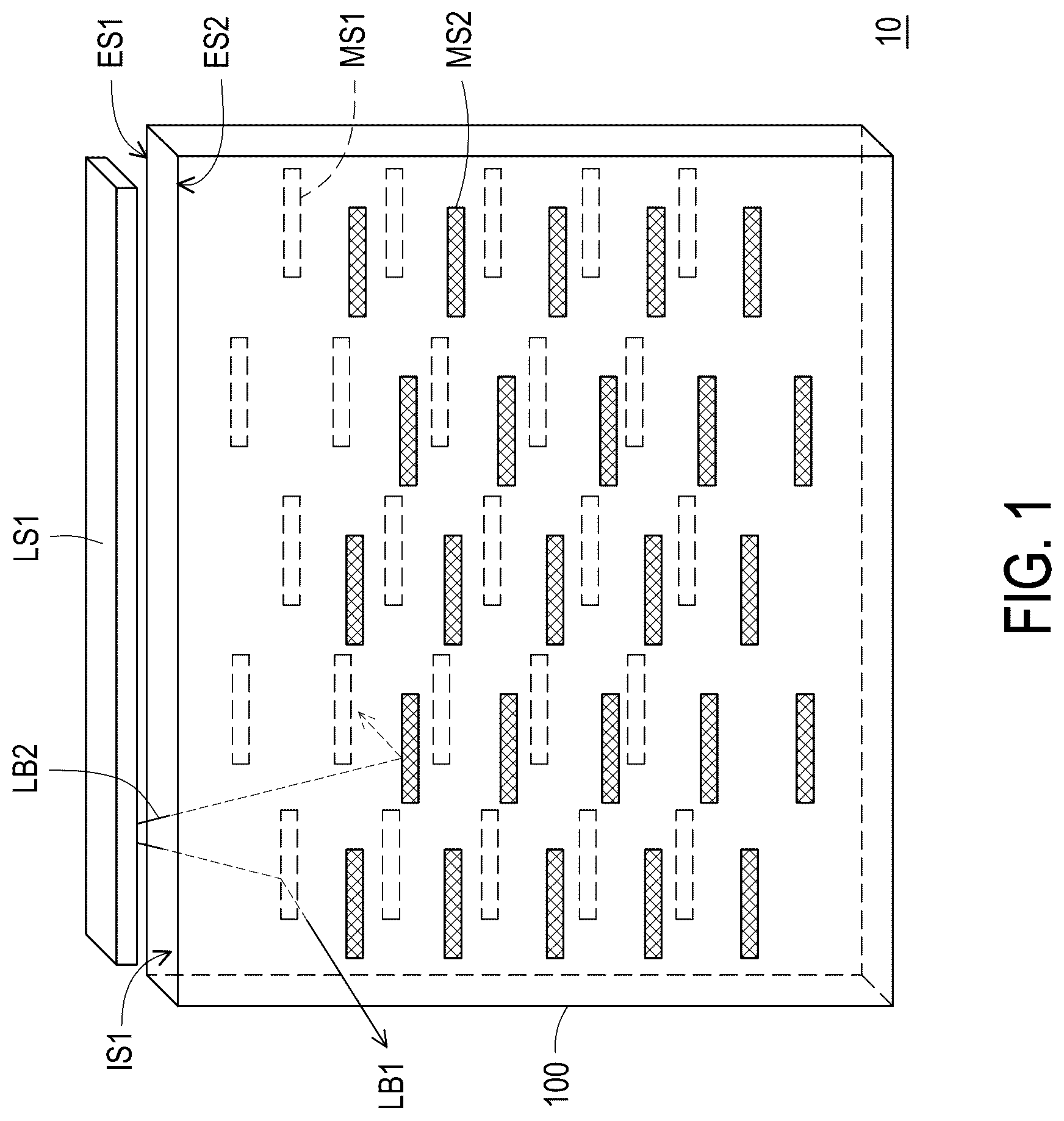
is a schematic three-dimensional view illustrating a lighting decoration module according to a first embodiment of the invention. is a schematic cross-sectional view illustrating the lighting decoration module depicted in . A is a schematic top view illustrating the first optical microstructures or the second optical microstructures depicted in . B and C are schematic top views illustrating optical microstructures according to other variant embodiments of the invention.
With reference to and , a lighting decoration module 10 includes a light guide plate (LGP) 100 , a first light source LS 1 , a plurality of first optical microstructures MS 1 , and a plurality of second optical microstructures MS 2 . The LGP 100 has a first light incident surface IS 1 , a first light exit surface ES 1 , and a second light exit surface ES 2 , and the first light exit surface ES 1 and the second light exit surface ES 2 connect the first light incident surface IS 1 and are opposite to each other. The first light source LS 1 is located on one side of the first light incident surface IS 1 of the LGP 100 and disposed corresponding to the first light incident surface IS 1 . The first optical microstructures MS 1 are disposed on the first light exit surface ES 1 of the LGP 100 . The second optical microstructures MS 2 are disposed on the second light exit surface ES 2 of the LGP 100 .
Note that each of the plurality of first optical microstructures MS 1 has a first surface RS 1 facing the first light source LS 1 and a first backlight surface BS 1 facing away from the first light source LS 1 , and a first angle A 1 between the first surface RS 1 and the first light exit surface ES 1 is greater than or equal to 40 degrees and less than or equal to 60 degrees. Each of the plurality of second optical microstructures MS 2 has a second surface RS 2 facing the first light source LS 1 and a second backlight surface BS 2 facing away from the first light source LS 1 , and a second angle A 2 between the second surface RS 2 and the second light exit surface ES 2 is greater than or equal to 40 degrees and less than or equal to 60 degrees.
For instance, a first light beam LB 1 emitted by the first light source LS 1 may be transmitted in the LGP 100 and emitted from the second light exit surface ES 2 of the LGP 100 after the first light beam LB 1 is reflected by the first surface RS 1 of each of the plurality of first optical microstructure MS 1 . A second light beam LB 2 emitted by the first light source LS 1 may be transmitted in the LGP 100 and emitted from the first light exit surface ES 1 of the LGP 100 after the second light beam LB 2 is reflected by the second surface RS 2 of each of the plurality of second optical microstructure MS 2 . More particularly, through the first optical microstructures MS 1 disposed on the first light exit surface ES 1 , a portion of the light beam (such as the first light beam LB 1 ) emitted by the first light source LS 1 may be guided to the second light exit surface ES 2 and may then exit; through the second optical microstructures MS 2 disposed on the second light exit surface ES 2 , another portion of the light beam (such as the second light beam LB 2 ) emitted by the first light source LS 1 may be guided to the first light exit surface ES 1 and may then exit.
Therefore, in the embodiment, a first pattern may be displayed on one side of the second light exit surface ES 2 of the LGP 100 through arrangement and distribution of the first optical microstructures MS 1 on the first light exit surface ES 1 , and a second pattern may be displayed on one side of the first light exit surface ES 1 of the LGP 100 through arrangement and distribution of the second optical microstructures MS 2 on the second light exit surface ES 2 . The first pattern and the second pattern may be the same or different from each other. That is, the lighting decoration module 10 provided in this embodiment is able to display patterns on both sides.
In the embodiment, the first optical microstructures MS 1 are, for instance, concave structures recessed from the first light exit surface ES 1 toward the second light exit surface ES 2 , for instance, and the second optical microstructures MS 2 are, for instance, concave structures recessed from the second light exit surface ES 2 toward the first light exit surface ES 1 . Therefore, the first surface RS 1 of each of the plurality of first optical microstructure MS 1 is located between the first backlight surface BS 1 and the first light incident surface IS 1 (or the first light source LS 1 ), and the second surface RS 2 of each of the plurality of second optical microstructure MS 2 is located between the second backlight surface BS 2 and the first light incident surface IS 1 .
However, the invention is not limited thereto. In another embodiment not shown in the drawings, the first optical microstructures may also be convex structures protruding from the first light exit surface toward a direction away from the second light exit surface, and the second optical microstructures may also be convex structures protruding from the second light exit surface toward a direction away from the first light exit surface. Therefore, the first backlight surface of each of the plurality of first optical microstructure may also be located between the first surface and the first light incident surface IS 1 , and the second backlight surface of each of the plurality of second optical microstructure may also be located between the second surface and the first light incident surface IS 1 . In still another embodiment not shown in the drawings, the optical microstructures on one light exit surface of the LGP may be convex structures, while the optical microstructures on the other light exit surface may be concave structures.
In the embodiment, a profile of an orthogonal projection of the first optical microstructures MS 1 on the first light exit surface ES 1 or a profile of an orthogonal projection of the second optical microstructures MS 2 on the second light exit surface ES 2 may have a bar shape (as shown in A ), which should however not be construed as a limitation to the invention. In another variant embodiment, a profile of an orthogonal projection of first optical microstructures MS 1 -A on the first light exit surface ES 1 or a profile of an orthogonal projection of the second optical microstructures MS 2 -A on the second light exit surface ES 2 may have a crescent shape (as shown in the B ), where an edge of a first surface RS 1 -A of each of the plurality of first optical microstructure MS 1 -A connecting the first light exit surface ES 1 or an edge of a second surface RS 2 -A of each of the plurality of second optical microstructure MS 2 -A connecting the second light exit surface ES 2 is a convex curve protruding toward the light incident surface of the LGP.
In yet another variant embodiment, a profile of an orthogonal projection of first optical microstructures MS 1 -B on the first light exit surface ES 1 or a profile of an orthogonal projection of second optical microstructures MS 2 -B on the second light exit surface ES 2 may be circular (as shown in C ), where the optical microstructures may be conical structures recessed from the light exit surfaces (i.e., concave structures whose circular diameter gradually decreases from openings of the concave structures toward bottoms of the concave structures), and an edge of a first surface RS 1 -B connecting the first light exit surface ES 1 or an edge of a second surface RS 2 -B connecting the second light exit surface ES 2 is an arc protruding toward the light incident surface of the LGP.
Another embodiment will be provided hereinafter to elaborate the invention, where the same component will be marked by the same reference numbers, and the description of the same technical content will be omitted. The omitted content may be referred to as those provided above and thus will not be repeated hereinafter.
is a schematic three-dimensional view illustrating a lighting decoration module according to a second embodiment of the invention. With reference to , the difference between a lighting decoration module 10 A provided in this embodiment and the lighting decoration module 10 depicted in lies in that the second surface of each of the plurality of second optical microstructure is arranged in a different manner. Specifically, in the embodiment, the lighting decoration module 10 A may further include a second light source LS 2 disposed on one side of the second light incident surface IS 2 of the LGP 100 .
In particular, the first light incident surface IS 1 of the LGP 100 connects the second light incident surface IS 2 . That is, the first light source LS 1 and the second light source LS 2 are disposed on two adjacent sides of the LGP 100 . In the embodiment, the second surface of each of the plurality of second optical microstructure MS 2 -C on the second light exit surface ES 2 faces the second light source LS 2 (or the second light incident surface IS 2 ).
For instance, a second light beam LB 2 ″ emitted by the second light source LS 2 may be transmitted in the LGP 100 , reflected by the second optical microstructures MS 2 -C, and then emitted from the first light exit surface ES 1 of the LGP 100 . More specifically, in the embodiment, the first light beam LB 1 provided by the first light source LS 1 serves to display patterns formed by the first optical microstructures MS 1 on one side of the second light exit surface ES 2 of the LGP 100 , and the second light beam LB 2 ″ provided by the second light source LS 2 serves to display patterns formed by second optical microstructures MS 2 -C on one side of the first light exit surface ES 1 of the LGP 100 .
is a schematic three-dimensional view illustrating a lighting decoration module according to a third embodiment of the invention. A and B are schematic cross-sectional views illustrating the lighting decoration module depicted in in an arrangement direction of the first light source and the LGP and in an arrangement direction of the second light source and the LGP. With reference to , A and B , the difference between a lighting decoration module 10 B provided in this embodiment and the lighting decoration module 10 A depicted in lies in that the number of patterns that can be displayed by the respective lighting decoration modules is different.
In detail, according to the embodiment, the lighting decoration module 10 B may further include a plurality of third optical microstructures MS 3 and a plurality of fourth optical microstructures MS 4 . The third optical microstructures MS 3 are disposed on the first light exit surface ES 1 of the LGP 100 . These fourth optical microstructures MS 4 are disposed on the second light exit surface ES 2 of the LGP 100 .
Note that each of the plurality of third optical microstructures MS 3 has a third surface RS 3 facing the second light source LS 2 and a third backlight surface BS 3 facing away from the second light source LS 2 , and a third angle A 3 between the third surface RS 3 and the first light exit surface ES 1 is greater than or equal to 40 degrees and less than or equal to 60 degrees. Each of the plurality of fourth optical microstructures MS 4 has a fourth surface RS 4 facing the first light source LS 1 and a fourth backlight surface BS 4 facing away from the first light source LS 1 , and a fourth angle A 4 between the fourth surface RS 4 and the second light exit surface ES 2 is greater than or equal 40 degrees and less than or equal to 60 degrees.
More specifically, in the embodiment, the first surface RS 1 of each of the plurality of first optical microstructure MS 1 on the first light exit surface ES 1 and the third surface RS 3 of each of the plurality of third optical microstructure MS 3 are disposed toward different light sources, respectively, and the second surface RS 2 of each of the plurality of second optical microstructure MS 2 -C on the second light exit surface ES 2 and the fourth surface RS 4 of each of the plurality of fourth optical microstructure MS 4 are disposed toward different light sources, respectively.
For instance, the first light beam LB 1 emitted by the first light source LS 1 and the third light beam LB 3 emitted by the second light source LS 2 may be transmitted in the LGP 100 , respectively reflected by the first surface RS 1 of each of the plurality of first optical microstructure MS 1 and the third surface RS 3 of each of the plurality of third optical microstructure MS 3 , and then emitted from the second light exit surface ES 2 of the LGP 100 . The second light beam LB 2 ″ emitted by the second light source LS 2 and the fourth light beam LB 4 emitted by the first light source LS 1 may be transmitted within the LGP 100 , respectively reflected by the second surface RS 2 of each of the plurality of second optical microstructure MS 2 -C and the fourth surface RS 4 of each of the plurality of fourth optical microstructure MS 4 , and then emitted from the first light exit surface ES 1 of the LGP 100 .
Through the first optical microstructures MS 1 and the third optical microstructures MS 3 disposed on the first light exit surface ES 1 , a portion of the light beam (such as the first light beam LB 1 ) emitted by the first light source LS 1 and a portion of the light beam (such as the third light beam LB 3 ) emitted by the second light source LS 2 may be guided to the second light exit surface ES 2 and may then exit, and via the second optical microstructures MS 2 -C and the fourth optical microstructures MS 4 disposed on the second light exit surface ES 2 , another portion of the light beam (such as the fourth light beam LB 4 ) emitted by the first light source LS 1 and another portion of the light beam (such as the second light beam LB 2 ″) emitted by the second light source LS 2 may be guided to the first light exit surface ES 1 and may then exit.
Therefore, under the irradiation of the first light source LS 1 , a first pattern may be displayed on one side of the second light exit surface ES 2 of the LGP 100 through arrangement and distribution of the plurality of first optical microstructures MS 1 on the first light exit surface ES 1 , and a fourth pattern may be displayed on one side of the first light exit surface ES 1 of the LGP 100 through arrangement and distribution of the plurality of fourth optical microstructures MS 4 on the second light exit surface ES 2 . Under the irradiation of the second light source LS 2 , a second pattern may be displayed on one side of the first light exit surface ES 1 of the LGP 100 through arrangement and distribution of the plurality of second optical microstructures MS 2 -C on the second light exit surface ES 2 , and a third pattern may be displayed on one side of the second light exit surface ES 2 of the LGP 100 through arrangement and distribution of the plurality of third optical microstructures MS 3 on the first light exit surface ES 1 . That is, the lighting decoration module 10 B provided in this embodiment is capable of performing the function of displaying four patterns on both sides, and the two patterns displayed on the same side of the LGP 100 may be independently controlled by the first light source LS 1 and the second light source LS 2 , respectively.
Similar to the first optical microstructures MS 1 , the third optical microstructures MS 3 are, for instance, concave structures recessed from the first light exit surface ES 1 toward the second light exit surface ES 2 . Similar to the second optical microstructures MS 2 -C, the fourth optical microstructures MS 4 are, for instance, concave structures recessed from the second light exit surface ES 2 toward the first light exit surface ES 1 . Therefore, the third surface RS 3 of each of the plurality of third optical microstructure MS 3 is located between the third backlight surface BS 3 and the second light incident surface IS 2 (or the second light source LS 2 ), and the fourth surface RS 4 of each of the plurality of fourth optical microstructure MS 4 is located between the fourth backlight surface BS 4 and the first light incident surface IS 1 (or the first light source LS 1 ).
Since the profile of the orthogonal projection of the optical microstructures on the corresponding light exit surface according to this embodiment is similar to the profile of the orthogonal projection of the optical microstructures depicted in A , detailed descriptions may be derived from the relevant paragraphs in the previous embodiment and will not be provided hereinafter.
is a schematic three-dimensional view illustrating a lighting decoration module according to a fourth embodiment of the invention. A to D are schematic cross-sectional views illustrating the lighting decoration module depicted in in an arrangement direction of the first light source and the LGP, in an arrangement direction of the second light source and the LGP, in an arrangement direction of the third light source and the LGP, and in an arrangement direction of the fourth light source and the LGP. With reference to to D , compared to the lighting decoration module 10 B depicted in , a lighting decoration module 10 C provided in this embodiment may further include a third light source LS 3 , a fourth light source LS 4 , a plurality of fifth optical microstructures MS 5 , a plurality of sixth optical microstructures MS 6 , a plurality of seventh optical microstructures MS 7 , and a plurality of eighth optical microstructures MS 8 . The third light source LS 3 is disposed on one side of a third light incident surface IS 3 of the LGP 100 , and the fourth light source LS 4 is disposed on one side of a fourth light incident surface IS 4 of the LGP 100 . Here, the third light incident surface IS 3 is opposite to the first light incident surface IS 1 and connects the second light incident surface IS 2 and the fourth light incident surface IS 4 . The fourth light incident surface IS 4 is opposite to the second light incident surface IS 2 and connects the first light incident surface IS 1 and the third light incident surface IS 3 .
In this embodiment, the plurality of fifth optical microstructures MS 5 and the plurality of seventh optical microstructures MS 7 are disposed on the first light exit surface ES 1 of the LGP 100 . The plurality of sixth optical microstructures MS 6 and the plurality of eighth optical microstructures MS 8 are disposed on the second light exit surface ES 2 of the LGP 100 .
Note that each of the plurality of fifth optical microstructures MS 5 has a fifth surface RS 5 facing the third light source LS 3 and a fifth backlight surface BS 5 facing away from the third light source LS 3 , and a fifth angle A 5 between the fifth surface RS 5 and the first light exit surface ES 1 is greater than or equal 40 degrees and less than or equal to 60 degrees. Each of the plurality of sixth optical microstructures MS 6 has a sixth surface RS 6 facing the third light source LS 3 and a sixth backlight surface BS 6 facing away from the third light source LS 3 , and a sixth angle A 6 between the sixth surface RS 6 and the second light exit surface ES 2 is greater than or equal 40 degrees and less than or equal to 60 degrees.
Each of the plurality of seventh optical microstructures MS 7 has a seventh surface RS 7 facing the fourth light source LS 4 and a seventh backlight surface BS 7 facing away from the fourth light source LS 4 , and a seventh angle A 7 between the seventh surface RS 7 and the first light exit surface ES 1 is greater than or equal 40 degrees and less than or equal to 60 degrees. Each of the plurality of eighth optical microstructures MS 8 has an eighth surface RS 8 facing the fourth light source LS 4 and an eighth backlight surface BS 8 facing away from the fourth light source LS 4 , and an eighth angle A 8 between the eighth surface RS 8 and the second light exit surface ES 2 is greater than or equal 40 degrees and less than or equal to 60 degrees.
More specifically, in this embodiment, on the first light exit surface ES 1 , the first surface RS 1 of each of the plurality of first optical microstructure MS 1 , the third surface RS 3 of each of the plurality of third optical microstructure MS 3 , the fifth surface RS 5 of each of the plurality of fifth optical microstructure MS 5 , and the seventh surface RS 7 of each of the plurality of seventh optical microstructure MS 7 are disposed towards different light sources, respectively. Similarly, on the second light exit surface ES 2 , the second surface RS 2 of each of the plurality of second optical microstructure MS 2 , the fourth surface RS 4 of each of the plurality of fourth optical microstructure MS 4 , the sixth surface RS 6 of each of the plurality of sixth optical microstructure MS 6 , and the eighth surface RS 8 of each of the plurality of eighth optical microstructure MS 8 are disposed towards different light sources, respectively.
For instance, the first light beam LB 1 emitted by the first light source LS 1 , the third light beam LB 3 emitted by the second light source LS 2 , a fifth light beam LB 5 emitted by the third light source LS 3 , and a seventh light beam LB 7 emitted by the fourth light source LS 4 may be transmitted in the LGP 100 and emitted from the second light exit surface ES 2 of the LGP 100 after the first light beam LB 1 is reflected by the first surface RS 1 of each of the plurality of first optical microstructure MS 1 , the third light beam LB 3 is reflected by the third surface RS 3 of each of the plurality of third optical microstructure MS 3 , the fifth light beam LB 5 is reflected by the fifth surface RS 5 of each of the plurality of fifth optical microstructure MS 5 , and the seventh light beam LB 7 is reflected by the seventh surface RS 7 of each of the plurality of seventh optical microstructure MS 7 .
Similarly, the second light beam LB 2 ″ emitted by the second light source LS 2 , the fourth light beam LB 4 emitted by the first light source LS 1 , a sixth light beam LB 6 emitted by the third light source LS 3 , and an eighth light beam LB 8 emitted by the fourth light source LS 4 may be transmitted in the LGP and emitted from the first light exit surface ES 1 of the LGP 100 after the second light beam LB 2 ″ is reflected by the second surface RS 2 of each of the plurality of second optical microstructure MS 2 , the fourth light beam LB 4 is reflected by the fourth surface RS 4 of each of the plurality of fourth optical microstructure MS 4 , the sixth light beam LB 6 is reflected by the sixth surface RS 6 of each of the plurality of sixth optical microstructure MS 6 , and the eighth light beam LB 8 is reflected by the eighth surface RS 8 of each of the plurality of eighth optical microstructure MS 8 .
Through the plurality of first optical microstructures MS 1 , the plurality of third optical microstructures MS 3 , the plurality of fifth optical microstructures MS 5 , and the plurality of seventh optical microstructures MS 7 disposed on the first light exit surface ES 1 , a portion of the light beam (such as the first light beam LB 1 ) emitted by the first light source LS 1 , a portion of the light beam (such as the third light beam LB 3 ) emitted by the second light source LS 2 , a portion of the light beam (such as the fifth light beam LB 5 ) emitted by the third light source LS 3 , and a portion of the light beam (such as the seventh light beam LB 7 ) emitted by the fourth light source LS 4 may be guided to the second light exit surface ES 2 and may then exit.
Similarly, by the plurality of second optical microstructures MS 2 -C, the plurality of fourth optical microstructures MS 4 , the plurality of sixth optical microstructures MS 6 , and the plurality of eighth optical microstructures MS 8 disposed on the second light exit surface ES 2 , another portion of the light beam (such as the fourth light beam LB 4 ) emitted by the first light source LS 1 , another portion of the light beam (such as the second light beam LB 2 ″) emitted by second light source LS 2 , another portion of the light beam (such as the sixth light beam LB 6 ) emitted by the third light source LS 3 , and another portion of the light beam (such as the eighth light beam LB 8 ) emitted by the fourth light source LS 4 may be guided to the first light exit surface ES 1 and may then exit.
Therefore, under the irradiation of the first light source LS 1 , a first pattern may be displayed on one side of the second light exit surface ES 2 of the LGP 100 through arrangement and distribution of the plurality of first optical microstructures MS 1 on the first light exit surface ES 1 , and a fourth pattern may be displayed on one side of the first light exit surface ES 1 of the LGP 100 through arrangement and distribution of the plurality of fourth optical microstructures MS 4 on the second light exit surface ES 2 . Under the illumination of the second light source LS 2 , a second pattern may be displayed on one side of the first light exit surface ES 1 of the LGP 100 through arrangement and distribution of the plurality of second optical microstructures MS 2 -C on the second light exit surface ES 2 , and a third pattern may be displayed on one side of the second light exit surface ES 2 of the LGP 100 through arrangement and distribution of the plurality of third optical microstructures MS 3 on the first light exit surface ES 1 .
In another aspect, under the irradiation of the third light source LS 3 , a fifth pattern may be displayed on one side of the second light exit surface ES 2 of the LGP 100 through arrangement and distribution of the plurality of fifth optical microstructures MS 5 on the first light exit surface ES 1 , and a sixth pattern may be displayed on one side of the first light exit surface ES 1 of the LGP 100 through arrangement and distribution of the plurality of sixth optical microstructures MS 6 on the second light exit surface ES 2 . Under the irradiation of the fourth light source LS 4 , a seventh pattern may be displayed on one side of the second light exit surface ES 2 of the LGP 100 through arrangement and distribution of the plurality of seventh optical microstructures MS 7 on the first light exit surface ES 1 , and an eighth pattern may be displayed on one side of the first light exit surface ES 1 of the LGP 100 through arrangement and distribution of the plurality of eighth optical microstructures MS 8 on the second light exit surface ES 2 .
That is, the lighting decoration module 10 C provided in this embodiment is capable of performing the function of displaying eight patterns on both sides, and the four patterns displayed on the same side of the LGP 100 may be independently controlled by the first light source LS 1 , the second light source LS 2 , the third Light source LS 3 , and the fourth light source LS 4 , respectively.
Similar to the plurality of first optical microstructures MS 1 and the plurality of third optical microstructures MS 3 , the plurality of fifth optical microstructures MS 5 and the plurality of seventh optical microstructures MS 7 are, for instance, concave structures recessed from the first light exit surface ES 1 toward the second light exit surface ES 2 . Similar to the plurality of second optical microstructures MS 2 -C and the plurality of fourth optical microstructures MS 4 , the plurality of sixth optical microstructures MS 6 and the plurality of eighth optical microstructures MS 8 are, for instance, concave structures recessed from the second light exit surface ES 2 toward the first light exit surface ES 1 . Therefore, the fifth surface RS 5 of each of the plurality of fifth optical microstructures MS 5 is located between the fifth backlight surface BS 5 and the third light incident surface IS 3 (or the third light source LS 3 ), and the sixth surface RS 6 of each of the plurality of sixth optical microstructures MS 6 is located between the sixth backlight surface BS 6 and the third light incident surface IS 3 (or the third light source LS 3 ). The seventh surface RS 7 of each of the plurality of seventh optical microstructures MS 7 is located between the seventh backlight surface BS 7 and the fourth light incident surface IS 4 (or the fourth light source LS 4 ), and the eighth surface RS 8 of each of the plurality of eighth optical microstructures MS 8 is located between the eighth backlight surface BS 8 and the fourth light incident surface IS 4 (or the fourth light source LS 4 ). Since the profile of the orthogonal projection of the optical microstructures on the corresponding light exit surface according to this embodiment is similar to the profile of the orthogonal projection of the optical microstructures depicted in A , detailed descriptions may be derived from the relevant paragraphs in the previous embodiment and will not be provided hereinafter.
is a schematic cross-sectional view illustrating a lighting decoration module according to a fifth embodiment of the invention. With reference to , the difference between a lighting decoration module 20 provided in this embodiment and the lighting decoration module 10 depicted in lies in that the first surface of each of the plurality of first optical microstructures is arranged in a different manner. Specifically, in this embodiment, a first angle A 1 ″ between the first surface RS 1 -C of each of the plurality of first optical microstructures MS 1 -C and the first light exit surface ES 1 is greater than or equal to 15 degrees and less than or equal to 35 degrees. Similar to the lighting decoration module respectively provided in each of the previous embodiments, the second angle A 2 between the second surface RS 2 of each of the plurality of second optical microstructures MS 2 provided in this embodiment and the second light exit surface ES 2 is greater than or equal to 40 degrees and less than or equal to 60 degrees.
Although the distribution range of the first angle A 1 ″ of the first surface RS 1 -C of each of the plurality of first optical microstructures MS 1 -C is different from the distribution range of the first angle A 1 of the first surface RS 1 of each of the plurality of first optical microstructures MS 1 depicted in , the manner in which the first backlight surface BS 1 -C is arranged relative to the first light exit surface ES 1 may still be similar to the manner in which the first backlight surface BS 1 of each of the plurality of first optical microstructures MS 1 is arranged relative to the first light exit surface ES 1 as shown in , which should not be construed as a limitation to the invention.
For instance, after the first light beam LB 1 ″ emitted by the first light source LS 1 is transmitted in the LGP 100 and reflected by the first surface RS 1 -C, an exit angle of the first light beam LB 1 ″ leaving the LGP 100 may be greater than or equal to 30 degrees and less than or equal to 50 degrees. The exit angle is, for instance, an angle between an exit direction of the first light beam LB 1 ″ from the second light exit surface ES 2 and a normal direction of the second light exit surface ES 2 . In addition, after the second light beam LB 2 emitted by the first light source LS 1 is transmitted in the LGP 100 and reflected by the second surface RS 2 , an exit direction of the second light beam LB 2 leaving the LGP 100 is relatively close to a normal direction of the first light exit surface ES 1 (e.g., the vertical direction in ).
Namely, in the lighting decoration module 20 provided in this embodiment, the light patterns of the exit light on one side of the first light exit surface ES 1 are rather concentrated and positive, while the light patterns of the exit light on one side of the second light exit surface ES 2 are rather dispersed. Therefore, the lighting decoration module 20 is not only able to perform the aforesaid function of displaying patterns but also capable of providing illumination. For instance, the lighting decoration module 20 provided in this embodiment may serve as a cover plate of a case of a computer host. In such an application scenario, the second light exit surface ES 2 of the lighting decoration module 20 may face the inside of the case, while the first light exit surface ES 1 of the lighting decoration module 20 may face away from the inside of the case.
When the first light source LS 1 is powered on, the first light beam LB 1 ″ emitted by the first light source LS 1 may be reflected by the plurality of first optical microstructures MS 1 -C and then guided to the inside of the case, and the second light beam LB 2 emitted by the first light source LS 1 may be reflected by the plurality of second optical microstructures MS 2 and emitted toward a direction away from the computer host. Therefore, the user may clearly see the inside of the case through the LGP 100 while seeing image patterns formed by the plurality of second optical microstructures MS 2 on the second light exit surface ES 2 .
By contrast, in the conventional lighting decoration module that provides the single-side light output, although the user may clearly see the image patterns presented on the LGP, the device inside the case cannot be clearly seen due to the insufficient illumination beam. In other words, the lighting decoration module 20 provided in this embodiment may provide a better visual experience than the conventional lighting decoration module when the lighting decoration module 200 is applied on the cover plate of the case.
In order to further improve the non-directivity required for illumination, according to this embodiment, the plurality of first optical microstructures MS 1 -C on the first light exit surface ES 1 may be conical structures as shown in C ; that is, the profile of the orthogonal projection of each of the plurality of first optical microstructures MS 1 -C on the first light exit surface ES 1 may be circular. On the contrary, in order to meet the directivity requirement of displaying the patterns, the profile of the orthogonal projection of each of the plurality of second optical microstructures MS 2 on the second light exit surface ES 2 may have a bar shape (as shown in A ) or a crescent shape (as shown in B ).
In particular, the limited range of the first angle A 1 ″ of the first surface RS 1 -C of each of the plurality of first optical microstructures MS 1 -C on the first light exit surface ES 1 (i.e., greater than or equal to 15 degrees and less than or equal to 35 degrees) and the limited range of the second angle A 2 of the second surface RS 2 of each of the plurality of second optical microstructures MS 2 on the second light exit surface ES 2 (i.e., the range from 40 degrees to 60 degrees) provided in this embodiment may also be applicable to each of the previous embodiments to meet the requirements of displaying a plurality of patterns and illumination at the same time, which will not be further described hereinafter.
To sum up, in the lighting decoration module provided in one or more embodiments of the invention, two kinds of optical microstructures are respectively disposed on the two opposite light exit surfaces of the LGP. When the angles between the surfaces of the two types of optical microstructures facing the light source and the corresponding light exit surfaces are greater than or equal to 40 degrees and less than or equal to 60 degrees, the lighting decoration module is allowed to achieve the double-sided display effects on both sides of the two light exit surfaces. When the angle between the surface of one of the two types of optical microstructures facing the light source and the corresponding light exit surface is are within a range from 15 degrees to 35 degrees, and the angle between the surface of the other of the two types of optical microstructures facing the light source and the corresponding light exit surface is within a range from 40 degrees to 60 degree, the lighting decoration module is allowed to achieve a single-sided display effect on one side of one of the light exit surfaces and provide illumination on one side of the other light exit surface.
The foregoing description of the preferred embodiments of the invention has been presented for purposes of illustration and description. It is not intended to be exhaustive or to limit the invention to the precise form or to exemplary embodiments disclosed. Accordingly, the foregoing description should be regarded as illustrative rather than restrictive. Obviously, many modifications and variations will be apparent to practitioners skilled in this art. The embodiments are chosen and described in order to best explain the principles of the invention and its best mode practical application, thereby to enable persons skilled in the art to understand the invention for various embodiments and with various modifications as are suited to the particular use or implementation contemplated. It is intended that the scope of the invention be defined by the claims appended hereto and their equivalents in which all terms are meant in their broadest reasonable sense unless otherwise indicated. Therefore, the term “the invention”, “the present invention” or the like does not necessarily limit the claim scope to a specific embodiment, and the reference to particularly preferred exemplary embodiments of the invention does not imply a limitation on the invention, and no such limitation is to be inferred. The invention is limited only by the spirit and scope of the appended claims. Moreover, these claims may refer to use “first”, “second”, etc. following with noun or element. Such terms should be understood as a nomenclature and should not be construed as giving the limitation on the number of the elements modified by such nomenclature unless specific number has been given. The abstract of the disclosure is provided to comply with the rules requiring an abstract, which will allow a searcher to quickly ascertain the subject matter of the technical disclosure of any patent issued from this disclosure. It is submitted with the understanding that it will not be used to interpret or limit the scope or meaning of the claims. Any advantages and benefits described may not apply to all embodiments of the invention. It should be appreciated that variations may be made in the embodiments described by persons skilled in the art without departing from the scope of the present invention as defined by the following claims. Moreover, no element and component in the present disclosure is intended to be dedicated to the public regardless of whether the element or component is explicitly recited in the following claims.
Figures (10)
Citations
This patent cites (42)
- US10883670
- US11187841
- US2007/0127264
- US2012/0188792
- US2013/0070482
- US2014/0198524
- US2015/0235508
- US2015/0268404
- US2016/0238777
- US2016/0306097
- US2018/0267344
- US2019/0094442
- US2019/0353837
- US2019/0361164
- US2020/0233142
- US2022/0003916
- US1627104
- US100381914
- US101449309
- US102425745
- US102681083
- US104864362
- US105913783
- US106663398
- US207817246
- US109212654
- US110622236
- USS4810920
- US2003045214
- US2006075362
- US2012156132
- US2015118128
- US2015156317
- US2015158317
- US2016157582
- US6402812
- US200923500
- US1350395
- US201406561
- US201614290
- US201618062
- US1574061