Electronic Component Having Element Body and Internal Conductors and Electronic Component Device
Abstract
An electronic component includes: an element body including first and second end surfaces opposing each other and a side surface coupling the first and second end surfaces; first and second internal conductors in the element body; a first external electrode on the first end surface; a second external electrode on the second end surface; and first and second external conductors on the side surface. The first and second external conductors are separated from the first and second external electrodes. The first internal conductor is electrically connected to the first external electrode and the first external conductor. The second internal conductor is electrically connected to the second external electrode and the second external conductor. The first external conductor is located between the first external electrode and the second external conductor. The second external conductor is located between the second external electrode and the first external conductor.
Claims (14)
1 . An electronic component, comprising: an element body including a first end surface and a second end surface opposing each other and a side surface coupling the first end surface and the second end surface; a plurality of internal conductors in the element body; a first external electrode on the first end surface and a second external electrode on the second end surface, each including an electrode layer in which migration is relatively prone to occur; and a first external conductor and a second external conductor disposed in a direction in which the first end surface and the second end surface oppose each other and separated from the first external electrode and the second external electrode, on the side surface, each including a conductor layer in which migration is less prone to occur than in the electrode layer, wherein the plurality of internal conductors includes a first internal conductor electrically connected to the first external electrode and the first external conductor and a second internal conductor electrically connected to the second external electrode and the second external conductor, the first internal conductor and the second internal conductor opposing each other in a direction orthogonal to the direction in which the first end surface and the second end surface oppose each other, the first external conductor is located between the first external electrode and the second external conductor, the second external conductor is located between the second external electrode and the first external conductor, and a first shortest distance between the first external electrode and the first external conductor and a second shortest distance between the second external electrode and the second external conductor are smaller than a shortest distance between the first external conductor and the second external conductor.
13 . An electronic component, comprising: an element body including a first end surface and a second end surface opposing each other and a side surface coupling the first end surface and the second end surface; a plurality of internal conductors in the element body; a first external electrode on the first end surface and a second external electrode on the second end surface, each including an electrode layer in which migration is relatively prone to occur; and a first external conductor and a second external conductor disposed in a direction in which the first end surface and the second end surface oppose each other and separated from the first external electrode and the second external electrode, on the side surface, each including a conductor layer in which migration is less prone to occur than in the electrode layer, wherein the plurality of internal conductors includes a first internal conductor electrically connected to the first external electrode and the first external conductor and a second internal conductor electrically connected to the second external electrode and the second external conductor, the first external conductor is located between the first external electrode and the second external conductor, the second external conductor is located between the second external electrode and the first external conductor, the side surface includes a first main surface arranged to include a mounting surface, a second main surface opposing the first main surface, and a pair of side surfaces that are adjacent to the first main surface, the second main surface, the first end surface, and the second end surface and oppose each other, the electrode layer includes a conductive resin layer continuously covering a part of the main surface, a part of a corresponding end surface of the first end surface and the second end surface, and a part of each of the pair of side surfaces, the first internal conductor opposes the second internal conductor in a direction in which the pair of side surfaces oppose each other, and is physically connected to a portion included in the first external conductor and located on the first main surface, the second internal conductor is physically connected to a portion included in the second external conductor and located on the first main surface, each of the first external conductor and the second external conductor is disposed over the first main surface and a portion of each of the pair of side surfaces, and a first height of a portion included in each of the first external conductor and the second external conductor and located on the portion of each of the pair of side surfaces in a direction orthogonal to the first main surface is larger than or equal to a second height of the conductive resin layer in the direction orthogonal to the first main surface.
14 . An electronic component, comprising: an element body including a first end surface and a second end surface opposing each other and a side surface coupling the first end surface and the second end surface; a plurality of internal conductors in the element body; a first external electrode on the first end surface and a second external electrode on the second end surface, each including an electrode layer in which migration is relatively prone to occur; and a first external conductor and a second external conductor disposed in a direction in which the first end surface and the second end surface oppose each other and separated from the first external electrode and the second external electrode, on the side surface, each including a conductor layer in which migration is less prone to occur than in the electrode layer, wherein the plurality of internal conductors includes a first internal conductor electrically connected to the first external electrode and the first external conductor and a second internal conductor electrically connected to the second external electrode and the second external conductor, the first external conductor is located between the first external electrode and the second external conductor, the second external conductor is located between the second external electrode and the first external conductor, the side surface includes a first main surface arranged to include a mounting surface, a second main surface opposing the first main surface, and a pair of side surfaces that are adjacent to the first main surface, the second main surface, the first end surface, and the second end surface and oppose each other, the electrode layer includes a conductive resin layer continuously covering a part of the main surface, a part of a corresponding end surface of the first end surface and the second end surface, and a part of each of the pair of side surfaces, the first internal conductor opposes the second internal conductor in a direction in which the first main surface and the second main surface oppose each other, and is physically connected to a portion included in the first external conductor and located on at least one side surface of the pair of side surfaces, the second internal conductor is physically connected to a portion included in the second external conductor and located on at least one side surface of the pair of side surfaces, each of the first external conductor and the second external conductor is disposed over the first main surface and a portion of each of the pair of side surfaces, and a first height of a portion included in each of the first external conductor and the second external conductor and located on the portion of each of the pair of side surfaces in a direction orthogonal to the first main surface is larger than or equal to a second height of the conductive resin layer in the direction orthogonal to the first main surface.
Show 11 dependent claims
2 . The electronic component according to claim 1 , wherein the element body has a rectangular parallelepiped shape, the side surface includes a first side surface, a second side surface, a third side surface, and a fourth side surface that are adjacent to the end surface and the second end surface, and the first external conductor and the second external conductor are disposed over the first side surface, the second side surface, the third side surface, and the fourth side surface.
3 . The electronic component according to claim 2 , wherein the first side surface and the second side surface oppose each other, the first internal conductor is physically connected to a portion included in the first external conductor and located on the first side surface, and the second internal conductor is physically connected to a portion included in the second external conductor and located on the second side surface.
4 . The electronic component according to claim 2 , wherein the first internal conductor is physically connected to a portion included in the first external conductor and located on the first side surface, and the second internal conductor is physically connected to a portion included in the second external conductor and located on the first side surface.
5 . The electronic component according to claim 1 , wherein the first internal conductor is connected to the first external conductor at a plurality of portions of the first internal conductor, and the second internal conductor is connected to the second external conductor at a plurality of portions of the second internal conductor.
6 . The electronic component according to claim 1 , wherein the side surface includes a first main surface arranged to include a mounting surface, a second main surface opposing the first main surface, and a pair of side surfaces that are adjacent to the first main surface, the second main surface, the first end surface, and the second end surface and oppose each other, the electrode layer includes a conductive resin layer continuously covering a part of the main surface, a part of a corresponding end surface of the first end surface and the second end surface, and a part of each of the pair of side surfaces, the first internal conductor opposes the second internal conductor in a direction in which the pair of side surfaces oppose each other, and is physically connected to a portion included in the first external conductor and located on the first main surface, and the second internal conductor is physically connected to a portion included in the second external conductor and located on the first main surface.
7 . The electronic component according to claim 6 , wherein each of the first external conductor and the second external conductor is disposed over the first main surface and a portion of each of the pair of side surfaces.
8 . The electronic component according to claim 7 , wherein a first height of a portion included in each of the first external conductor and the second external conductor and located on the portion of each of the pair of side surfaces in a direction orthogonal to the first main surface is larger than or equal to a second height of the conductive resin layer in the direction orthogonal to the first main surface.
9 . The electronic component according to claim 1 , wherein the side surface includes a first main surface arranged to include a mounting surface, a second main surface opposing the first main surface, and a pair of side surfaces that are adjacent to the first main surface, the second main surface, the first end surface, and the second end surface and oppose each other, the electrode layer includes a conductive resin layer continuously covering a part of the main surface, a part of a corresponding end surface of the first end surface and the second end surface, and a part of each of the pair of side surfaces, the first internal conductor opposes the second internal conductor in a direction in which the first main surface and the second main surface oppose each other, and is physically connected to a portion included in the first external conductor and located on at least one side surface of the pair of side surfaces, and the second internal conductor is physically connected to a portion included in the second external conductor and located on at least one side surface of the pair of side surfaces.
10 . The electronic component according to claim 9 , wherein an internal conductor, among the plurality of internal conductors, between the second main surface and an end edge included in the conductive resin layer and located closer to the second main surface, in the direction in which the first main surface and the second main surface oppose each other, is not electrically connected to either the first external conductor or the second external conductor.
11 . The electronic component according to claim 1 , wherein the electrode layer includes a conductive resin layer including a plurality of silver particles, and the conductor layer includes a metal layer in which migration is less prone to occur than in silver.
12 . An electronic component device, comprising: the electronic component according to claim 1 ; and an electronic device on which the electronic component is mounted, the first external conductor and the second external conductor are not physically connected to the electronic device.
Full Description
Show full text →
CROSS-REFERENCE TO RELATED APPLICATIONS
This application is based upon and claims the benefit of priority from Japanese Patent Application No. 2023-013061, filed on Jan. 31, 2023. The entire contents of which are incorporated herein by reference.
BACKGROUND
Field
The present disclosure relates to an electronic component or an electronic component device.
Description of the Related Art
Known electronic components include an element body, a plurality of internal conductors in the element body, and a plurality of external electrodes on the element body (see, for example, Japanese Unexamined Patent Publication No. 2018-006501). Each of the plurality of internal conductors is connected to a corresponding external electrode of the plurality of external electrodes. Each of the plurality of external electrodes includes a conductive resin layer.
SUMMARY
The conductive resin layer includes, for example, a plurality of metal particles and a resin. In a configuration in which the external electrode includes the conductive resin layer, migration may occur in the external electrode. The conductive resin layer is an example of an electrode layer in which migration is relatively prone to occur.
Migration is considered to occur due to the following events, for example.
An electric field acts on the electrode layer, and metal included in the electrode layer is ionized. Generated metal ion is attracted by an electric field between the external electrodes and migrates from the electrode layer. The electric field acting on the metal includes, for example, an electric field between the external electrodes or an electric field between the external electrode and an internal conductor in the element body. The metal ion migrating from the electrode layer react with, for example, an electron supplied from the internal conductor or the external electrode, and is deposited as metal on a surface of the element body.
One aspect of the present disclosure provides an electronic component reducing occurrence of migration. Another aspect of the present disclosure provides an electronic component device reducing occurrence of migration.
An electronic component according to one aspect of the present disclosure includes: an element body including a first end surface and a second end surface opposing each other and a side surface coupling the first end surface and the second end surface; a plurality of internal conductors in the element body; a first external electrode on the first end surface and a second external electrode on the second end surface; and a first external conductor and a second external conductor disposed in a direction in which the first end surface and the second end surface oppose each other and separated from the first external electrode and the second external electrode, on the side surface. Each of the first external electrode and the second external electrode includes an electrode layer in which migration is relatively prone to occur. Each of the first external conductor and the second external conductor includes a conductor layer in which migration is less prone to occur than in the electrode layer. The plurality of internal conductors includes a first internal conductor electrically connected to the first external electrode and the first external conductor and a second internal conductor electrically connected to the second external electrode and the second external conductor. The first external conductor is located between the first external electrode and the second external conductor. The second external conductor is located between the second external electrode and the first external conductor.
In the one aspect described above, the electrode layer included in the first external electrode and the conductor layer included in the first external conductor are electrically connected to each other, and the electrode layer included in the second external electrode and the conductor layer included in the second external conductor are electrically connected to each other. When an electric field acts on the electrode layer, the electric field acts not only on the electrode layer but also on the conductor layer electrically connected to the electrode layer. The electric field tends not to be concentrated on the electrode layer, and the conductor layer reduces the electric field acting on the electrode layer. Therefore, even when an electric field acts on the electrode layer, metal included in the electrode layer tends not to be ionized. Migration tends not to occur in the electrode layer.
The first external conductor is located between the first external electrode and the second external conductor. The electrode layer included in the first external electrode and the conductor layer included in the first external conductor are electrically connected to each other. Therefore, when migration occurs in the electrode layer included in the first external electrode, the first external conductor prevents the migration from proceeding.
The second external conductor is located between the second external electrode and the first external conductor. The electrode layer included in the second external electrode and the conductor layer included in the second external conductor are electrically connected to each other. Therefore, when migration occurs in the electrode layer included in the second external electrode, the second external conductor prevents the migration from proceeding.
Consequently, the one aspect described above prevents the migration from proceeding.
In the one aspect described above, the element body may have a rectangular parallelepiped shape, and the side surface may include a first side surface, a second side surface, a third side surface, and a fourth side surface that are adjacent to the end surface and the second end surface. The first external conductor and the second external conductor may be disposed over the first side surface, the second side surface, the third side surface, and the fourth side surface.
A configuration in which the first external conductor and the second external conductor are disposed over the first side surface, the second side surface, the third side surface, and the fourth side surface reliably prevents the migration from proceeding.
In the one aspect described above, the first side surface and the second side surface may oppose each other. The first internal conductor may be physically connected to a portion included in the first external conductor and located on the first side surface. The second internal conductor may be physically connected to a portion included in the second external conductor and located on the second side surface.
In the one aspect described above, the first internal conductor may be physically connected to a portion included in the first external conductor and located on the first side surface. The second internal conductor may be physically connected to a portion included in the second external conductor and located on the first side surface.
In the one aspect described above, the first internal conductor may be connected to the first external conductor at a plurality of portions of the first internal conductor. The second internal conductor may be connected to the second external conductor at a plurality of portions of the second internal conductor.
A configuration in which the first internal conductor is connected to the first external conductor at the plurality of portions of the first internal conductor and the second internal conductor is connected to the second external conductor at the plurality of portions of the second internal conductor reliably prevents the migration from proceeding.
In the one aspect described above, a first shortest distance between the first external electrode and the first external conductor and a second shortest distance between the second external electrode and the second external conductor may be smaller than a shortest distance between the first external conductor and the second external conductor.
A configuration in which the first shortest distance and the second shortest distance are smaller than the shortest distance between the first external conductor and the second external conductor reduces a progress distance of the migration, even when the migration occurs in the electrode layer. Therefore, the first external electrode and the second external electrode tend not to be short-circuited.
In the one aspect described above, the side surface may include a first main surface arranged to include a mounting surface, a second main surface opposing the first main surface, and a pair of side surfaces that are adjacent to the first main surface, the second main surface, the first end surface, and the second end surface and oppose each other. The electrode layer may include a conductive resin layer continuously covering a part of the main surface, a part of a corresponding end surface of the first end surface and the second end surface, and a part of each of the pair of side surfaces. The first internal conductor may oppose the second internal conductor in a direction in which the pair of side surfaces oppose each other, and may be physically connected to a portion included in the first external conductor and located on the first main surface. The second internal conductor may be physically connected to a portion included in the second external conductor and located on the first main surface.
A configuration in which the conductive resin layer covers the part of the corresponding end surface decreases ESR (equivalent series resistance), as compared with a configuration in which a conductive resin layer covers an entire corresponding end surface.
A configuration in which the first internal conductor is physically connected to the portion, of the first external conductor, on the first main surface and the second internal conductor is physically connected to the portion, of the second external conductor, on the first main surface reliably prevents the migration from proceeding from the conductive resin layer, even in a configuration in which the first internal conductor opposes the second internal conductor in the direction in which the pair of side surfaces oppose each other.
In the one aspect described above, the side surface may include a first main surface arranged to include a mounting surface, a second main surface opposing the first main surface, and a pair of side surfaces that are adjacent to the first main surface, the second main surface, the first end surface, and the second end surface and oppose each other. The electrode layer may include a conductive resin layer continuously covering a part of the main surface, a part of a corresponding end surface of the first end surface and the second end surface, and a part of each of the pair of side surfaces. The first internal conductor may oppose the second internal conductor in a direction in which the first main surface and the second main surface oppose each other, and may be physically connected to a portion included in the first external conductor and located on at least one side surface of the pair of side surfaces. The second internal conductor may be physically connected to a portion included in the second external conductor and located on at least one side surface of the pair of side surfaces.
A configuration in which the conductive resin layer covers the part of the corresponding end surface decreases ESR, as compared with a configuration in which a conductive resin layer covers an entire corresponding end surface.
A configuration in which the first internal conductor is physically connected to the portion, of the first external conductor, on the at least one side surface and the second internal conductor is physically connected to the portion, of the second external conductor, on the at least one side surface reliably prevents the migration from proceeding from the conductive resin layer, even in a configuration in which the first internal conductor opposes the second internal conductor in the direction in which the first main surface and the second main surface oppose each other.
In the one aspect described above, an internal conductor, among the plurality of internal conductors, between the second main surface and an end edge included in the conductive resin layer and located closer to the second main surface, in the direction in which the first main surface and the second main surface oppose each other, may be not electrically connected to either the first external conductor or the second external conductor.
In the one aspect described above, each of the first external conductor and the second external conductor may be disposed over the first main surface and a portion of each of the pair of side surfaces.
A configuration in which each of the first external conductor and the second external conductor is disposed over the first main surface and the portion of each of the pair of side surfaces realizes easy formation of the first external conductor and the second external conductor, and reliably prevents the migration from proceeding.
In the one aspect described above, a first height of a portion included in each of the first external conductor and the second external conductor and located on the portion of each of the pair of side surfaces in a direction orthogonal to the first main surface may be larger than or equal to a second height of the conductive resin layer in the direction orthogonal to the first main surface.
A configuration in which the first height is larger than or equal to the second height reliably prevents the migration from proceeding.
In the one aspect described above, the electrode layer may include a conductive resin layer including a plurality of silver particles. The conductor layer may include a metal layer in which migration is less prone to occur than in silver.
A configuration in which the conductor layer includes the metal layer in which migration is less prone to occur than in silver reliably prevents the migration from proceeding, even in a configuration in which the conductive resin layer, of the electrode layer, includes the plurality of silver particles.
An electronic component device according to another aspect of the present disclosure includes: the electronic component according to the one aspect described above; and an electronic device on which the electronic component is mounted. The first external conductor and the second external conductor are not physically connected to the electronic device.
As described above, the other aspect described above prevents the migration from proceeding in the electronic component.
In the other aspect described above, the first external conductor and the second external conductor are not physically connected to the electronic device. Therefore, when an external force acts on the electronic component from the electronic device, the external force does not act on the element body through the first external conductor and the second external conductor.
The electronic device does not need to include a land pattern to which the first outer conductor and the second outer conductor are physically connected. Therefore, the other aspect described above prevents a configuration of the electronic device from being complicated.
BRIEF DESCRIPTION OF THE DRAWINGS
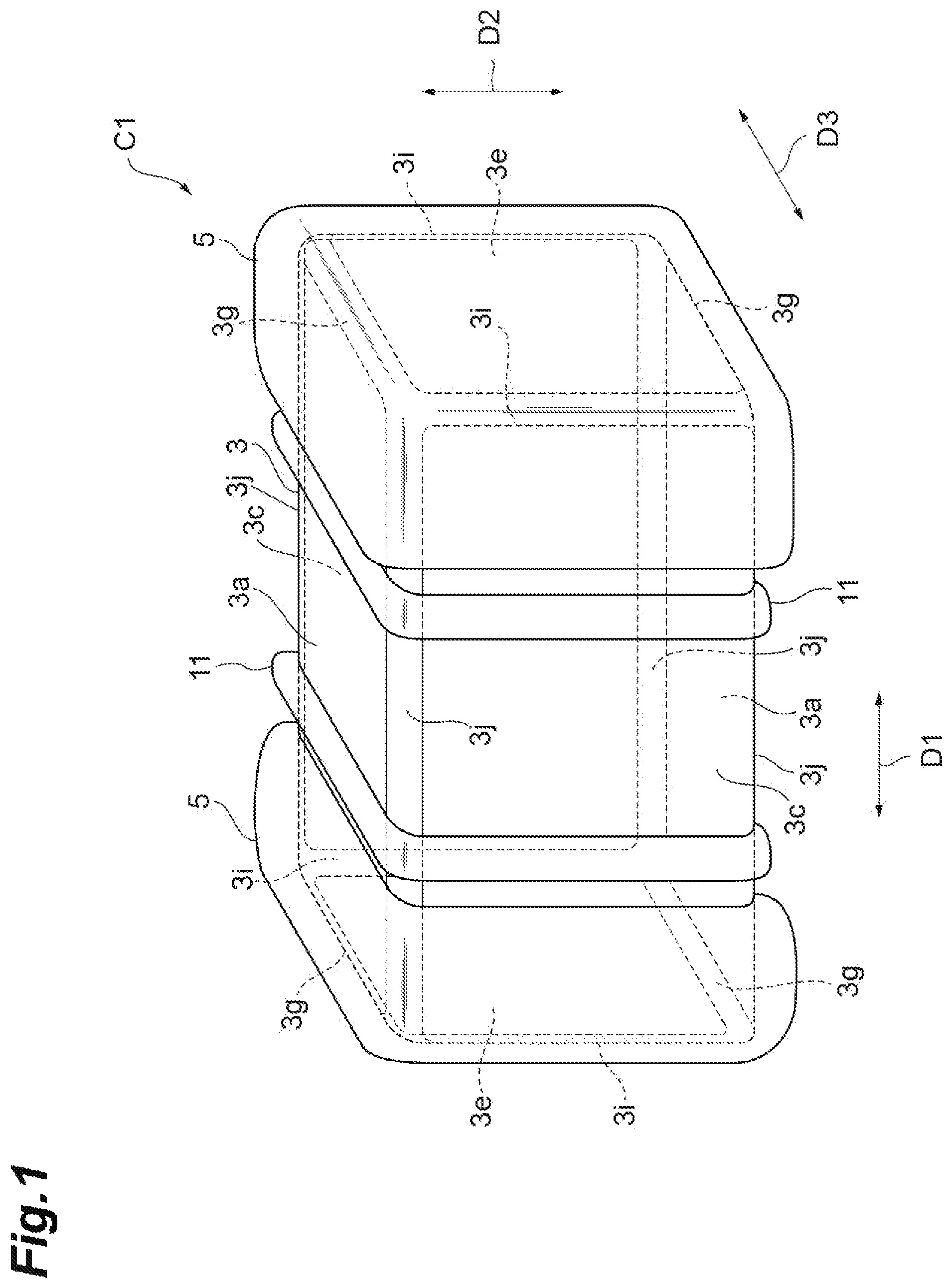
is a perspective view of a multilayer capacitor according to a first example;
is a view illustrating a cross-sectional configuration of the multilayer capacitor according to the first example;
is a view illustrating a cross-sectional configuration of the multilayer capacitor according to the first example;
is a view illustrating a cross-sectional configuration of the multilayer capacitor according to the first example;
is a view illustrating a cross-sectional configuration of the multilayer capacitor according to the first example;
is a view illustrating a cross-sectional configuration of a multilayer capacitor according to one modified example of the first example;
is a view illustrating a cross-sectional configuration of the multilayer capacitor according to the one modified example of the first example;
is a view illustrating a cross-sectional configuration of the multilayer capacitor according to the one modified example of the first example;
is a view illustrating a cross-sectional configuration of a multilayer capacitor according to another modified example of the first example;
is a view illustrating a cross-sectional configuration of the multilayer capacitor according to the other modified example of the first example;
is a perspective view of a multilayer capacitor according to a second example;
is a view illustrating a cross-sectional configuration of the multilayer capacitor according to the second example;
is a view illustrating a cross-sectional configuration of the multilayer capacitor according to the second example;
is a view illustrating a cross-sectional configuration of the multilayer capacitor according to the second example;
is a view illustrating a cross-sectional configuration of the multilayer capacitor according to the second example;
is a perspective view of a multilayer capacitor according to one modified example of the second example;
is a view illustrating a cross-sectional configuration of the multilayer capacitor according to the one modified example of the second example;
is a view illustrating a cross-sectional configuration of the multilayer capacitor according to the one modified example of the second example;
is a view illustrating a cross-sectional configuration of the multilayer capacitor according to the one modified example of the second example;
is a view illustrating an external electrode and an external conductor;
is a view illustrating a cross-sectional configuration of a multilayer capacitor according to another modified example of the second example;
is a view illustrating a cross-sectional configuration of the multilayer capacitor according to the other modified example of the second example;
is a view illustrating a cross-sectional configuration of the multilayer capacitor according to the other modified example of the second example;
is a view illustrating a cross-sectional configuration of the multilayer capacitor according to the other modified example of the second example; and
is a view illustrating a cross-sectional configuration of an electronic component device including the multilayer capacitor according to the first example.
DETAILED DESCRIPTION
In the following description, with reference to the drawings, the same reference numbers are assigned to the same components or to similar components having the same function, and overlapping description is omitted.
First Example
A configuration of a multilayer capacitor C 1 according to the first example will be described with reference to to 5 . is a perspective view of a multilayer capacitor according to the first example. , 3 , 4 , and 5 are views illustrating a cross-sectional configuration of the multilayer capacitor according to the first example.
In the first example, an electronic component includes, for example, the multilayer capacitor C 1 .
As illustrated in , the multilayer capacitor C 1 includes an element body 3 of a rectangular parallelepiped shape, a plurality of external electrodes 5 , and a plurality of external conductors 11 . For example, the multilayer capacitor C 1 includes a pair of external electrodes 5 . The pair of external electrodes 5 are disposed on an outer surface of the element body 3 . The pair of external electrodes 5 are separated from each other. The rectangular parallelepiped shape includes a rectangular parallelepiped shape in which corners and ridges are chamfered, or a rectangular parallelepiped shape in which the corners and ridges are rounded.
The element body 3 includes a pair of main surfaces 3 a opposing each other, a pair of side surfaces 3 c opposing each other, and a pair of end surfaces 3 e opposing each other. The pair of main surfaces 3 a , the pair of side surfaces 3 c , and the pair of end surfaces 3 e each have a substantially rectangular shape. The pair of main surfaces 3 a oppose each other in a second direction D 2 . The pair of side surfaces 3 c oppose each other in a third direction D 3 . The pair of end surfaces 3 e oppose each other in a first direction D 1 . A direction in which the pair of main surfaces 3 a oppose each other includes the second direction D 2 . A direction in which the pair of side surfaces 3 c oppose each other includes the third direction D 3 . A direction in which the pair of end surfaces 3 e oppose each other includes the first direction D 1 . The multilayer capacitor C 1 is solder-mounted on an electronic device. The electronic device includes, for example, a circuit board or an electronic component. In the multilayer capacitor C 1 , for example, the main surface 3 a or the side surface 3 c opposes the electronic device. The main surface 3 a or the side surface 3 c is arranged to constitute a mounting surface. The main surface 3 a or the side surface 3 c is the mounting surface.
The second direction D 2 includes a direction orthogonal to the main surfaces 3 a , and is orthogonal to the third direction D 3 . The second direction D 2 includes a direction intersecting the main surfaces 3 a . The first direction D 1 includes a direction parallel to the main surfaces 3 a and the side surfaces 3 c , and is orthogonal to the second direction D 2 and the third direction D 3 . The third direction D 3 is a direction orthogonal to the side surfaces 3 c , and the first direction D 1 includes a direction orthogonal to the end surfaces 3 e . For example, a length of the element body 3 in the first direction D 1 is larger than a length of the element body 3 in the second direction D 2 and larger than a length of the element body 3 in the third direction D 3 . The first direction D 1 includes a longitudinal direction of the element body 3 . The length of the element body 3 in the second direction D 2 and the length of the element body 3 in the third direction D 3 may be equal to each other. The length of the element body 3 in the second direction D 2 and the length of the element body 3 in the third direction D 3 may be different.
The pair of side surfaces 3 c extend in the second direction D 2 to couple the pair of main surfaces 3 a to each other. The pair of side surfaces 3 c also extend in the first direction D 1 . The pair of end surfaces 3 e extend in the second direction D 2 to couple the pair of main surfaces 3 a to each other. The pair of end surfaces 3 e also extend in the third direction D 3 .
For example, when one end surface 3 e includes a first end surface, the other end surface 3 e includes a second end surface.
Each of the main surfaces 3 a also includes a side surface included in the element body 3 . The side surface of the element body 3 includes the pair of main surfaces 3 a and the pair of side surfaces 3 c . For example, when one side surface 3 c includes a first side surface, the other side surface 3 c may include a second side surface, one main surface 3 a may include a third side surface, and another main surface 3 a may include a fourth side surface.
The element body 3 includes four ridge portions 3 g , four ridge portions 3 i , and four ridge portions 3 j . The ridge portions 3 g are located between the end surfaces 3 e and the main surfaces 3 a . The ridge portions 3 i are located between the end surfaces 3 e and the side surfaces 3 c . The ridge portions 3 j are located between the main surfaces 3 a and the side surfaces 3 c . For example, the ridge portions 3 g , 3 i , and 3 j are rounded to be curved. For example, the element body 3 is subjected to what is called a round chamfering process. The end surfaces 3 e and the main surfaces 3 a are indirectly adjacent to each other with the ridge portion 3 g interposed therebetween. The end surfaces 3 e and the side surfaces 3 c are indirectly adjacent to each other with the ridge portion 3 i interposed therebetween. The main surfaces 3 a and the side surfaces 3 c are indirectly adjacent to each other with the ridge portion 3 j interposed therebetween.
The element body 3 is configured through laminating a plurality of dielectric layers in the second direction D 2 . The element body 3 includes a plurality of laminated dielectric layers. In the element body 3 , a lamination direction of the plurality of dielectric layers coincides with the second direction D 2 . Each dielectric layer includes, for example, a sintered body of a ceramic green sheet containing a dielectric material. Examples of the dielectric material include dielectric ceramics. Examples of the dielectric ceramics include BaTiO 3 -based, Ba(Ti, Zr)O 3 -based, or (Ba, Ca)TiO 3 -based dielectric ceramics. In the actual element body 3 , each of the dielectric layers is integrated to such an extent that a boundary between the dielectric layers cannot be visually recognized.
The length of the element body 3 in the second direction D 2 is a height of the element body 3 . The length of the element body 3 in the third direction D 3 is a width of the element body 3 . The length of the element body 3 in the first direction D 1 is a length of the element body 3 . For example, the height of the element body 3 is 0.1 to 2.5 mm, the width of the element body 3 is 0.1 to 5.0 mm, and the length of the element body 3 is 0.2 to 5.7 mm. For example, the height of the element body 3 is 2.5 mm, the width of the element body 3 is 2.5 mm, and the length of the element body 3 is 3.2 mm.
As illustrated in , the external electrodes 5 are disposed at both ends of the element body 3 in the first direction D 1 . Each external electrode 5 is disposed on a corresponding end surface 3 e of the pair of end surfaces 3 e . For example, each external electrode 5 is disposed on the pair of main surfaces 3 a , the pair of side surfaces 3 c , and the end surface 3 e . The external electrode 5 includes a plurality of electrode portions 5 a , 5 c , and 5 e , as illustrated in to 4 . The electrode portion 5 a is disposed on the main surface 3 a . The electrode portion 5 a may be disposed on the ridge portion 3 g . The electrode portion 5 c is disposed on the side surface 3 c . The electrode portion 5 c may be disposed on the ridge portion 3 i . The electrode portion 5 e is disposed on the end surface 3 e . The external electrode 5 also includes an electrode portion disposed on the ridge portion 3 j.
Each external electrode 5 is formed on five surfaces of the pair of main surfaces 3 a , the pair of side surfaces 3 c , and the end surface 3 e as well as the ridge portions 3 g , 3 i , and 3 j . The electrode portions 5 a , 5 b , 5 c , and 5 e adjacent to each other are coupled and are electrically connected to each other. As illustrated in , the external electrode 5 includes a first electrode layer E 1 , a second electrode layer E 2 , and a third electrode layer E 3 . The third electrode layer E 3 is arranged to include the outermost layer of the external electrode 5 . Each of the electrode portions 5 a , 5 c , and 5 e includes the first electrode layer E 1 , the second electrode layer E 2 , and the third electrode layer E 3 .
The first electrode layer E 1 of the electrode portion 5 a is disposed on the main surface 3 a and on the ridge portion 3 g . The first electrode layer E 1 of the electrode portion 5 a covers a part of the main surface 3 a and the entire ridge portion 3 g . The first electrode layer E 1 of the electrode portion 5 a is in contact with the above-described part of the main surface 3 a and the entire ridge portion 3 g . In the electrode portion 5 a , the first electrode layer E 1 is in direct contact with the element body 3 . The above-described part of the main surface 3 a includes a partial region, of the main surface 3 a , closer to the end surface 3 e . The first electrode layer E 1 of the electrode portion 5 a is located on the main surface 3 a . The first electrode layer E 1 may not be formed on the main surface 3 a . The first electrode layer E 1 may not be disposed on the main surface 3 a.
The second electrode layer E 2 of the electrode portion 5 a is disposed on the first electrode layer E 1 and on the main surface 3 a . In the electrode portion 5 a , the second electrode layer E 2 covers the first electrode layer E 1 and a part of the main surface 3 a . In the electrode portion 5 a , the second electrode layer E 2 is in direct contact with the first electrode layer E 1 and the main surface 3 a . The second electrode layer E 2 of the electrode portion 5 a includes a portion directly covering the first electrode layer E 1 and a portion directly covering the main surface 3 a . In the electrode portion 5 a , the portion included in the second electrode layer E 2 and directly covering the first electrode layer E 1 indirectly covers the main surface 3 a . The second electrode layer E 2 of the electrode portion 5 a is located on the main surface 3 a . The main surface 3 a includes a region covered with the second electrode layer E 2 and a region exposed from the second electrode layer E 2 .
The third electrode layer E 3 of the electrode portion 5 a is disposed on the second electrode layer E 2 . In the electrode portion 5 a , the third electrode layer E 3 covers the second electrode layer E 2 . In the electrode portion 5 a , the third electrode layer E 3 is in contact with the entire second electrode layer E 2 . In the electrode portion 5 a , the third electrode layer E 3 is in direct contact with the second electrode layer E 2 . In the electrode portion 5 a , the third electrode layer E 3 is not in direct contact with the first electrode layer E 1 . The third electrode layer E 3 of the electrode portion 5 a is located on the main surface 3 a.
The first electrode layer E 1 of the electrode portion 5 c is disposed on the side surface 3 c and on the ridge portion 3 i . The first electrode layer E 1 of the electrode portion 5 c covers a part of the side surface 3 c and the entire ridge portion 3 i . The first electrode layer E 1 of the electrode portion 5 c is in contact with the above-described part of the side surface 3 c and on the entire ridge portion 3 i . In the electrode portion 5 c , the first electrode layer E 1 is in direct contact with the element body 3 . The above-described part of the side surface 3 c includes a partial region, of the side surface 3 c , closer to the end surface 3 e . The first electrode layer E 1 of the electrode portion 5 c is located on the side surface 3 c . The first electrode layer E 1 may not be formed on the side surface 3 c . The first electrode layer E 1 may not be disposed on the side surface 3 c.
The second electrode layer E 2 of the electrode portion 5 c is disposed on the first electrode layer E 1 and on the side surface 3 c . In the electrode portion 5 c , the second electrode layer E 2 covers the first electrode layer E 1 and a part of the side surface 3 c . In the electrode portion 5 c , the second electrode layer E 2 is in direct contact with the first electrode layer E 1 and the side surface 3 c . The second electrode layer E 2 of the electrode portion 5 c includes a portion directly covering the first electrode layer E 1 and a portion directly covering the side surface 3 c . In the electrode portion 5 c , the portion included in the second electrode layer E 2 and directly covering the first electrode layer E 1 indirectly covers the side surface 3 c . The second electrode layer E 2 of the electrode portion 5 c is located on the side surface 3 c . The side surface 3 c includes a region covered with the second electrode layer E 2 and a region exposed from the second electrode layer E 2 .
The third electrode layer E 3 of the electrode portion 5 c is disposed on the second electrode layer E 2 . In the electrode portion 5 c , the third electrode layer E 3 covers the second electrode layer E 2 . In the electrode portion 5 c , the third electrode layer E 3 is in contact with the entire second electrode layer E 2 . In the electrode portion 5 c , the third electrode layer E 3 is in direct contact with the second electrode layer E 2 . The third electrode layer E 3 of the electrode portion 5 c is located on the side surface 3 c.
The first electrode layer E 1 of the electrode portion 5 e is disposed on the end surface 3 e . The first electrode layer E 1 of the electrode portion 5 e covers the entire end surface 3 e . The first electrode layer E 1 of the electrode portion 5 e is in contact with the entire end surface 3 e . In the electrode portion 5 e , the first electrode layer E 1 is in direct contact with the end surface 3 e.
The second electrode layer E 2 of the electrode portion 5 e is disposed on the first electrode layer E 1 . In the electrode portion 5 e , the second electrode layer E 2 covers the entire first electrode layer E 1 . In the electrode portion 5 e , the second electrode layer E 2 is in direct contact with the first electrode layer E 1 . The second electrode layer E 2 of the electrode portion 5 e directly covers the first electrode layer E 1 and indirectly covers the end surface 3 e . The second electrode layer E 2 of the electrode portion 5 e is located on the end surface 3 e.
The third electrode layer E 3 of the electrode portion 5 e is disposed on the second electrode layer E 2 . In the electrode portion 5 e , the third electrode layer E 3 covers the entire second electrode layer E 2 . In the electrode portion 5 e , the third electrode layer E 3 is in contact with the entire second electrode layer E 2 . In the electrode portion 5 e , the third electrode layer E 3 is in direct contact with the second electrode layer E 2 . The third electrode layer E 3 of the electrode portion 5 e is located on the end surface 3 e.
The first electrode layer E 1 is formed from sintering electrically conductive paste applied onto the surface of the element body 3 . The first electrode layer E 1 covers the above-described part of each of the main surfaces 3 a , the above-described part of each of the side surfaces 3 c , the end surface 3 e , and the ridge portions 3 g , 3 i , and 3 j . The first electrode layer E 1 is formed from sintering a metal component (metal particles) included in the electrically conductive paste. The metal component contained in the electrically conductive paste includes, for example, metal particles. The first electrode layer E 1 includes a sintered metal layer. The first electrode layer E 1 includes the sintered metal layer formed on the element body 3 . For example, the first electrode layer E 1 includes a sintered metal layer made of Cu. The first electrode layer E 1 may include a sintered metal layer made of Ni. The first electrode layer E 1 includes a base metal. The electrically conductive paste includes, for example, particles made of Cu or Ni, a glass component, an organic binder, and an organic solvent. The first electrode layer E 1 included in each of the electrode portions 5 a , 5 c , and 5 e is integrally formed.
The second electrode layer E 2 is formed from curing electrically conductive resin paste applied onto the first electrode layer E 1 . The second electrode layer E 2 is formed over the first electrode layer E 1 and the element body 3 . The first electrode layer E 1 includes an underlying metal layer for forming the second electrode layer E 2 . The second electrode layer E 2 includes an electrically conductive resin layer that covers the first electrode layer E 1 . The conductive resin paste includes, for example, a resin, an electrically conductive material, and an organic solvent. The resin includes, for example, a thermosetting resin. The conductive material includes, for example, metal particles. The metal particles include, for example, silver particles. For example, the second electrode layer E 2 includes a plurality of silver particles. The thermosetting resin is, for example, a phenol resin, an acrylic resin, a silicone resin, an epoxy resin, or a polyimide resin. The second electrode layer E 2 is in contact with a part of the ridge portion 3 j . The second electrode layer E 2 included in each of the electrode portions 5 a , 5 c , and 5 e is integrally formed.
The third electrode layer E 3 is formed on the second electrode layer E 2 through a plating method. The third electrode layer E 3 may have a multilayer structure. In this case, the third electrode layer E 3 includes, for example, an Ni plating layer and a solder plating layer. The Ni plating layer is formed on the second electrode layer E 2 . The solder plating layer is formed on the Ni plating layer. The solder plating layer covers the Ni plating layer. The Ni plating layer has better solder leach resistance than the metal included in the second electrode layer E 2 . The third electrode layer E 3 may include an Sn plating layer, a Cu plating layer, or an Au plating layer instead of the Ni plating layer. The solder plating layer includes, for example, an Sn plating layer, an Sn—Ag alloy plating layer, an Sn—Bi alloy plating layer, or an Sn—Cu alloy plating layer. The third electrode layer E 3 included in each of the electrode portions 5 a , 5 c , and 5 e is integrally formed.
As illustrated in to 5 , the multilayer capacitor C 1 includes a pair of external conductors 11 . The pair of external conductors 11 are disposed on the outer surface of the element body 3 . The pair of external conductors 11 are disposed in the first direction D 1 , on the side surface. The pair of external conductors 11 are disposed in the first direction D 1 , on the pair of main surfaces 3 a and the pair of side surfaces 3 c . The pair of external conductors 11 are separated from each other in the first direction D 1 . The external conductors 11 are separated from the external electrodes 5 . The pair of external conductors 11 are disposed between the pair of external electrodes 5 in the first direction D 1 .
The external conductors 11 are disposed over the pair of main surfaces 3 a and the pair of side surfaces 3 c . Each external conductor 11 includes portions 11 a each disposed on a corresponding main surface 3 a of the pair of main surfaces 3 a , and portions 11 c each disposed on a corresponding side surface 3 c of the pair of side surfaces 3 c . Each external conductor 11 includes the pair of portions 11 a and the pair of portions 11 c . For example, the portions 11 a and the portions 11 c are integrally formed. Each external conductor 11 is also disposed on each ridge portion 3 j . The portions 11 a and the portions 11 c are not only physically connected to each other but also electrically connected to each other.
One external conductor 11 of the pair of external conductors 11 and One external electrode 5 of the pair of external electrodes 5 are adjacent to each other in the first direction D 1 . The one external conductor 11 and the electrode portions 5 a and 5 c of the one external electrode 5 are adjacent to each other in the first direction D 1 . Another external conductor 11 of the pair of external conductors 11 and another external electrode 5 of the pair of external electrodes 5 are adjacent to each other in the first direction D 1 . The other external conductor 11 and the electrode portions 5 a and 5 c of the other external electrode 5 are adjacent to each other in the first direction D 1 . The one external conductor 11 is located between the one external electrode 5 and the other external conductor 11 . The other external conductor 11 is located between the other external electrode 5 and the one external conductor 11 .
The portions 11 a are disposed between the electrode portions 5 a located on the same main surface 3 a on which the portions 11 a are disposed, and are separated from the electrode portions 5 a . The portion 11 a extends along an end edge of the electrode portion 5 a . The portion 11 a extends in the third direction D 3 .
A distance W 1 a between the electrode portion 5 a and the portion 11 a adjacent to each other in the first direction D 1 is smaller than a distance W 2 a between the pair of portions 11 a adjacent to each other in the first direction D 1 . The distance W 1 a is a shortest distance between the electrode portion 5 a and the portion 11 a in the first direction D 1 . The distance W 2 a is a shortest distance between the pair of portions 11 a in the first direction D 1 . The distance W 1 a between the portion 11 a included in the one external conductor 11 and the electrode portion 5 a included in the one external electrode 5 may be equal to or different from the distance W 1 a between the portion 11 a included in the other external conductor 11 and the electrode portion 5 a included in the other external electrode 5 . For example, when the distance W 1 a between the portion 11 a included in the one external conductor 11 and the electrode portion 5 a included in the one external electrode 5 includes a first shortest distance, the distance W 1 a between the portion 11 a included in the other external conductor 11 and the electrode portion 5 a included in the other external electrode 5 includes a second shortest distance.
The portions 11 c are disposed between the electrode portions 5 c located on the same side surface 3 c on which the portions 11 c are disposed, and are separated from the electrode portions 5 c . The portion 11 c extends along an end edge of the electrode portion 5 c . The portion 11 c extends in the second direction D 2 .
A distance W 1 c between the electrode portion 5 c and the portion 11 c adjacent to each other in the first direction D 1 is smaller than a distance W 2 c between the pair of portions 11 c adjacent to each other in the first direction D 1 . The distance W 1 c is a shortest distance between the electrode portion 5 c and the portion 11 c in the first direction D 1 . The distance W 2 c is a shortest distance between the pair of portions 11 c in the first direction D 1 . The distance W 1 c between the portion 11 c included in the one external conductor 11 and the electrode portion 5 c included in the one external electrode 5 may be equal to or different from the distance W 1 c between the portion 11 c included in the other external conductor 11 and the electrode portion 5 c included in the other external electrode 5 . For example, when the distance W 1 c between the portion 11 c included in the one external conductor 11 and the electrode portion 5 c included in the one external electrode 5 includes a first shortest distance, the distance W 1 a between the portion 11 c included in the other external conductor 11 and the electrode portion 5 c included in the other external electrode 5 includes a second shortest distance.
The distance W 1 a and the distance W 1 c may be equal to or different from each other. The distance W 2 a and the distance W 2 c may be equal to or different from each other.
The external conductor 11 includes a conductor layer 13 . The conductor layer 13 includes the pair of portions 11 a and the pair of portions 11 c . The conductor layer 13 includes, for example, a sintered metal layer. In this case, the conductor layer 13 includes a metal layer. The conductor layer 13 including the sintered metal layer is formed from sintering electrically conductive paste applied onto the surface of the element body 3 . The conductor layer 13 includes a sintered metal layer formed on the element body 3 . For example, the conductor layer 13 includes a sintered metal layer made of Cu. The electrically conductive paste includes, for example, particles made of Cu, a glass component, an organic binder, and an organic solvent. The conductor layer 13 may include a sintered metal layer made of Ni.
For example, Cu and N are electrically conductive materials in which migration is less prone to occur than in silver (silver particles included in the second electrode layer E 2 ). Generally, migration is relatively prone to occur in silver. The external electrode 5 includes the second electrode layer E 2 in which migration is relatively prone to occur. The external conductor 11 includes the conductor layer 13 in which migration is less prone to occur than in the second electrode layer E 2 . The conductor layer 13 does not substantially include silver.
A plating layer may be formed on the surface of the external conductor 11 . The plating layer may have, for example, the same configuration as that of the third electrode layer E 3 .
The conductor layer 13 may include a conductive resin layer. In a configuration in which the conductor layer 13 includes a conductive resin layer, the conductor layer 13 may be formed from curing electrically conductive resin paste applied onto the element body 3 . This conductive resin paste includes, for example, a resin, a plurality of electrically conductive particles, and an organic solvent. This resin includes, for example, a thermosetting resin. The electrically conductive particles include, for example, metal particles. The metal particles include, for example, copper particles. In a configuration in which the conductor layer 13 includes a conductive resin layer, the conductor layer 13 may include a plurality of copper particles. The thermosetting resin is, for example, a phenol resin, an acrylic resin, a silicone resin, an epoxy resin, or a polyimide resin. The electrically conductive particles included in the conductive resin layer included in the conductor layer 13 may include carbon particles. Even in a configuration in which the conductor layer 13 includes a conductive resin layer, the external conductor 11 includes the conductor layer 13 in which migration is less prone to occur than in the second electrode layer E 2 . Even in a configuration in which the conductor layer 13 includes a conductive resin layer, the conductor layer 13 does not substantially include silver.
As illustrated in to 5 , the multilayer capacitor C 1 includes a plurality of internal electrodes 7 and a plurality of internal electrodes 9 . Each of the internal electrodes 7 and 9 includes an internal conductor disposed in the element body 3 . A plurality of internal conductors included in the multilayer capacitor C 1 include the plurality of internal electrodes 7 and the plurality of internal electrodes 9 . For example, when the internal electrode 7 includes a first internal conductor, the internal electrode 9 includes a second internal conductor. In , for the sake of explanation, the internal electrodes 7 and 9 are intentionally illustrated so as to deviate from each other in the third direction D 3 .
Each of the internal electrodes 7 and 9 is made of an electrically conductive material that is commonly used as an internal conductor of a multilayer electronic component. The electrically conductive material includes, for example, a base metal. The electrically conductive material includes, for example, Ni or Cu. Each of the internal electrodes 7 and 9 is configured as a sintered body of electrically conductive paste containing the electrically conductive material described above. For example, the internal electrodes 7 and 9 are made of Ni.
The internal electrodes 7 and the internal electrodes 9 are disposed in different positions (layers) in the second direction D 2 . The internal electrodes 7 and the internal electrodes 9 are alternately disposed in the element body 3 to oppose each other in the second direction D 2 with an interval therebetween. The plurality of internal electrodes 7 and the plurality of internal electrodes 9 are alternately disposed in the second direction D 2 . The plurality of internal electrodes 7 and the plurality of internal electrodes 9 are disposed in the element body 3 to be distributed in the second direction D 2 . Each of the plurality of internal electrodes 7 and the plurality of internal electrodes 9 is located in a plane substantially parallel to the main surfaces 3 a . Each of the plurality of internal electrodes 7 and the plurality of internal electrodes 9 is disposed to extend in a direction intersecting the side surfaces 3 c . For example, each of the plurality of internal electrodes 7 and the plurality of internal electrodes 9 is disposed to extend in a direction substantially orthogonal to the side surfaces 3 c . The internal electrode 7 and the internal electrode 9 oppose each other in the second direction D 2 . The direction in which the internal electrode 7 and the internal electrode 9 oppose each other, that is, the second direction D 2 is orthogonal to a direction parallel to the main surfaces 3 a (third direction D 3 and first direction D 1 ).
The internal electrodes 7 and the internal electrodes 9 have different polarities from each other. One end of each of the internal electrodes 7 and 9 is exposed to a corresponding end surface 3 e of the pair of end surfaces 3 e . Each of the internal electrodes 7 and 9 includes the one end exposed to the corresponding end surface 3 e . One electrode portion 5 e entirely covers the one ends of the plurality of internal electrodes 7 . Another electrode portion 5 e entirely covers the one ends of the plurality of internal electrodes 9 . Each electrode portion 5 e is directly connected to corresponding internal electrodes of the plurality of internal electrodes 7 and 9 . Each external electrode 5 is electrically connected to the corresponding internal electrodes of the plurality of internal electrodes 7 and 9 . For example, the plurality of internal electrodes 7 are physically and electrically connected to one external electrode 5 of the pair of external electrodes 5 . The plurality of internal electrodes 9 are physically and electrically connected to another external electrode 5 of the pair of external electrodes 5 .
Each of the internal electrodes 7 and 9 is connected to a corresponding external conductor 11 of the pair of external conductors 11 . The internal electrodes 7 are electrically connected to the one external conductor 11 adjacent to the one external electrode 5 , in the first direction D 1 , to which the internal electrodes 7 are physically and electrically connected. The second electrode layer E 2 included in the one external electrode 5 and the one external conductor 11 are electrically connected through the internal electrodes 7 . The internal electrodes 9 are electrically connected to the other external conductor 11 adjacent to the other external electrode 5 , in the first direction D 1 , to which the internal electrodes 9 are physically and electrically connected. The second electrode layer E 2 included in the other external electrode 5 is electrically connected to the other external conductor 11 through the internal electrodes 9 .
The internal electrode 7 includes a pair of connection portions 7 a . Each of the pair of connection portions 7 a is exposed to a corresponding side surface 3 c of the pair of side surfaces 3 c . Each of the pair of connection portions 7 a includes an end exposed to the corresponding side surface 3 c . Each connection portion 7 a is physically and electrically connected to the portion 11 c disposed on the corresponding side surface 3 c at the end exposed to the corresponding side surface 3 c . The internal electrode 7 is physically connected to the corresponding external conductor 11 at a plurality of portions of the internal electrode 7 . For example, all internal electrodes 7 are physically connected to the corresponding external conductor 11 . However, it is not necessary for all internal electrodes 7 to be physically connected to the corresponding external conductor 11 . At least one of the plurality of internal electrodes 7 may be physically connected to the corresponding external conductor 11 .
The internal electrode 9 includes a pair of connection portions 9 a . Each of the pair of connection portions 9 a is exposed to a corresponding side surface 3 c of the pair of side surfaces 3 c . Each of the pair of connection portions 9 a includes an end exposed to the corresponding side surface 3 c . Each connection portion 9 a is physically and electrically connected to the portion 11 c disposed on the corresponding side surface 3 c at the end exposed to the corresponding side surface 3 c . The internal electrode 9 is physically connected to the corresponding external conductor 11 at a plurality of portions of the internal electrode 9 . For example, all internal electrodes 9 are physically connected to the corresponding external conductor 11 . However, it is not necessary for all internal electrodes 9 to be physically connected to the corresponding external conductor 11 . At least one of the plurality of internal electrodes 9 may be physically connected to the corresponding external conductor 11 . The connection portion 7 a and the connection portion 9 a exposed to the same side surface 3 c are separated from each other in the first direction D 1 .
The plurality of internal electrodes 7 include an internal electrode 7 A adjacent to the other main surface 3 a . The internal electrode 7 A opposes the second electrode layer E 2 included in the electrode portion 5 a that is electrically connected to the internal electrode 9 and located on the other main surface 3 a , for example, in the second direction D 2 . When the internal electrode 7 A and the second electrode layer E 2 that is electrically connected to the internal electrode 9 and located on the other main surface 3 a are viewed from, for example, the second direction D 2 , the internal electrode 7 A and the second electrode layer E 2 that is electrically connected to the internal electrode 9 and located on the other main surface 3 a overlap each other. Therefore, an electric field tends to be generated between the internal electrode 7 A and the second electrode layer E 2 that is electrically connected to the internal electrode 9 and located on the other main surface 3 a.
The plurality of internal electrodes 9 include an internal electrode 9 A adjacent to the one main surface 3 a . The internal electrode 9 A opposes the second electrode layer E 2 included in the electrode portion 5 a that is electrically connected to the internal electrode 7 and located on the one main surface 3 a , for example, in the second direction D 2 . When the internal electrode 9 A and the second electrode layer E 2 that is electrically connected to the internal electrode 7 and located on the one main surface 3 a are viewed from, for example, the second direction D 2 , the internal electrode 9 A and the second electrode layer E 2 that is electrically connected to the internal electrode 7 and located on the one main surface 3 a overlap each other. Therefore, an electric field tends to be generated between the internal electrode 9 A and the second electrode layer E 2 that is electrically connected to the internal electrode 7 and located on the one main surface 3 a.
The plurality of internal electrodes 7 oppose the second electrode layer E 2 included in the electrode portion 5 c that is electrically connected to the internal electrode 9 and located on each side surface 3 c , for example, in the third direction D 3 . When the plurality of internal electrodes 7 and the second electrode layer E 2 that is electrically connected to the internal electrode 9 and located on each side surface 3 c are viewed from, for example, the third direction D 3 , the plurality of internal electrodes 7 and the second electrode layer E 2 that is electrically connected to the internal electrode 9 and located on each side surface 3 c overlap each other. Therefore, an electric field tends to be generated between the plurality of internal electrodes 7 and the second electrode layer E 2 that is electrically connected to the internal electrode 9 and located on each side surface 3 c.
The plurality of internal electrodes 9 oppose the second electrode layer E 2 included in the electrode portion 5 c that is electrically connected to the internal electrode 7 and located on each side surface 3 c , for example, in the third direction D 3 . When the plurality of internal electrodes 9 and the second electrode layer E 2 that is electrically connected to the internal electrode 7 and located on each side surface 3 c are viewed from, for example, the third direction D 3 , the plurality of internal electrodes 9 and the second electrode layer E 2 that is electrically connected to the internal electrode 7 and located on each side surface 3 c overlap each other. Therefore, an electric field tends to be generated between the plurality of internal electrodes 9 and the second electrode layer E 2 that is electrically connected to the internal electrode 7 and located on each side surface 3 c.
The plurality of internal electrodes 7 oppose the external conductor 11 (conductor layer 13 ) that is electrically connected to the internal electrode 9 , for example, in the third direction D 3 . Therefore, an electric field may be generated between the plurality of internal electrodes 7 and the external conductor 11 that is electrically connected to the internal electrode 9 .
The plurality of internal electrodes 9 oppose the external conductor 11 (conductor layer 13 ) that is electrically connected to the internal electrode 7 , for example, in the third direction D 3 . Therefore, an electric field may be generated between the plurality of internal electrodes 9 and the external conductor 11 that is electrically connected to the internal electrode 7 .
In the multilayer capacitor C 1 , the second electrode layer E 2 included in the external electrode 5 and the conductor layer 13 included in the external conductor 11 adjacent to the external electrode 5 in the first direction D 1 are electrically connected to each other. When an electric field acts on the second electrode layer E 2 , the electric field acts not only on the second electrode layer E 2 but also on the conductor layer 13 electrically connected to the second electrode layer E 2 . The electric field tends not to be concentrated on the second electrode layer 2 , and the conductor layer 13 reduces the electric field acting on the second electrode layer E 2 . Therefore, even when an electric field acts on the second electrode layer E 2 , metal included in the second electrode layer E 2 tends not to be ionized. Migration tends not to occur in the second electrode layer E 2 .
Migration is less prone to occur in the conductor layer 13 than in the second electrode layer E 2 . Therefore, even when an electric field acts on the conductor layer 13 , the migration tends not to occur in the conductor layer 13 .
The one external conductor 11 is located between the external electrode 5 (second electrode layer E 2 ) electrically connected to the one external conductor 11 and the other external conductor 11 . Therefore, even when migration occurs in the second electrode layer E 2 included in the external electrode 5 electrically connected to the one external conductor 11 , the one external conductor 11 prevents the migration from proceeding.
The other external conductor 11 is located between the external electrode 5 (second electrode layer E 2 ) electrically connected to the other external conductor 11 and the one external conductor 11 . Therefore, even when migration occurs in the second electrode layer E 2 included in the external electrode 5 electrically connected to the other external conductor 11 , the other external conductor 11 prevents the migration from proceeding.
Consequently, the multilayer capacitor C 1 prevents the migration from proceeding.
In the multilayer capacitor C 1 , each external conductor 11 is disposed over the pair of main surfaces 3 a and the pair of side surfaces 3 c . Therefore, the multilayer capacitor C 1 reliably prevents the migration from proceeding.
In the multilayer capacitor C 1 , each of the plurality of internal electrodes 7 is physically connected to the corresponding external conductor 11 at the plurality of portions of each internal electrode 7 , and each of the plurality of internal electrodes 9 is physically connected to the corresponding external conductor 11 at the plurality of portions of each internal electrode 9 . Therefore, the multilayer capacitor C 1 reliably prevents the migration from proceeding.
In the multilayer capacitor C 1 , the distance W 1 a is smaller than the distance W 2 a , and the distance W 1 c is smaller than the distance W 2 c . Therefore, the multilayer capacitor C 1 reduces a progress distance of the migration, even when the migration occurs in the second electrode layer E 2 . Consequently, the pair of external electrodes 5 tend not to be short-circuited.
In the multilayer capacitor C 1 , the second electrode layer E 2 includes the plurality of silver particles, and the conductor layer 13 includes the metal layer in which migration is less prone to occur than in silver.
The multilayer capacitor C 1 reliably prevents the migration from proceeding, even in a configuration in which the second electrode layer E 2 includes the plurality of silver particles.
Next, a configuration of a multilayer capacitor C 1 according to one modified example of the first example will be described with reference to to 8 . , 7 , and 8 are views illustrating a cross-sectional configuration of a multilayer capacitor according to the one modified example of the first example.
The multilayer capacitor C 1 according to the one modified example is generally similar to or the same as the multilayer capacitor C 1 according to the first example described above. However, the one modified example is different from the above-described first example in a configuration of the internal electrodes 7 and 9 . Hereinafter, differences between the above-described first example and the one modified example will be mainly described. In , for the sake of explanation, the internal electrodes 7 and 9 are intentionally illustrated so as to deviate from each other in the third direction D 3 .
Each of the plurality of internal electrodes 7 includes one connection portion 7 a . Each internal electrode 7 includes only one connection portion 7 a . The connection portion 7 a is exposed to one side surface 3 c of the pair of side surfaces 3 c . The connection portion 7 a includes an end exposed to the one side surface 3 c . The connection portion 7 a is physically and electrically connected to the portion 11 c disposed on the one side surface 3 c , at the end exposed to the one side surface 3 c . Also in the one modified example, at least one internal electrode 7 among the plurality of internal electrodes 7 may be physically connected to the corresponding external conductor 11 .
Each of the plurality of internal electrodes 9 includes one connection portion 9 a . Each internal electrode 9 includes only one connection portion 9 a . The connection portion 9 a is exposed to another side surface 3 c of the pair of side surfaces 3 c . The connection portion 9 a includes an end exposed to the other side surface 3 c . The connection portion 9 a is physically and electrically connected to the portion 11 c disposed on the other side surface 3 c , at the end exposed to the other side surface 3 c . Also in the one modified example, at least one internal electrode 9 among the plurality of internal electrodes 9 may be physically connected to the corresponding external conductor 11 .
In the multilayer capacitor C 1 according to the one modified example, the internal electrode 7 is physically connected to the portion 11 c included in the corresponding external conductor 11 and located on the one side surface 3 c . The internal electrode 9 is physically connected to the portion 11 c included in the corresponding external conductor 11 and located on the other side surface 3 c.
Next, a configuration of a multilayer capacitor C 1 according to another modified example of the first example will be described with reference to . are views illustrating a cross-sectional configuration of a multilayer capacitor according to the other modified example of the first example.
The multilayer capacitor C 1 according to the other modified example is generally similar to or the same as the multilayer capacitor C 1 according to the one modified example described above. However, the other modified example is different from the above-described one modified example in a configuration of the internal electrodes 9 . Hereinafter, differences between the above-described one modified example and the other modified example will be mainly described. In , for the sake of explanation, the internal electrodes 7 and 9 are intentionally illustrated so as to deviate from each other in the third direction D 3 .
Each of the plurality of internal electrodes 9 includes one connection portion 9 a . Each internal electrode 9 includes only one connection portion 9 a . The connection portion 9 a is exposed to the side surface 3 c to which the connection portion 7 a is exposed. The connection portion 7 a and the connection portion 9 a are exposed to the same side surface 3 c . The connection portion 9 a includes an end exposed to the side surface 3 c to which the connection portion 7 a is exposed. The connection portion 9 a is physically and electrically connected to the portion 11 c disposed on the one side surface 3 c , at the end exposed to the side surface 3 c to which the connection portion 7 a is exposed.
In the multilayer capacitor C 1 according to the other modified example, the internal electrode 7 is physically connected to the portion 11 c included in the corresponding external conductor 11 and located on the one side surface 3 c . The internal electrode 9 is physically connected to the portion 11 c included in the corresponding external conductor 11 and located on the one side surface 3 c.
Second Example
A configuration of a multilayer capacitor C 2 according to the second example will be described with reference to to 15 . is a perspective view of a multilayer capacitor according to the second example. , 13 , 14 , and 15 are views illustrating a cross-sectional configuration of the multilayer capacitor according to the second example.
In the second example, an electronic component includes, for example, the multilayer capacitor C 2 . The multilayer capacitor C 2 is generally similar to or the same as the multilayer capacitor C 1 . However, the multilayer capacitor C 2 is different from the multilayer capacitor C 1 in a configuration of the plurality of external electrodes 5 and the internal electrodes 7 and 9 . Hereinafter, differences between the multilayer capacitor C 1 and the multilayer capacitor C 2 will be mainly described.
As illustrated in to 15 , the multilayer capacitor C 2 includes an element body 3 of a rectangular parallelepiped shape, a plurality of external electrodes 5 , a plurality of internal electrodes 7 , a plurality of internal electrodes 9 , and a plurality of external conductors 11 . For example, the multilayer capacitor C 2 includes a pair of external electrodes 5 and a pair of external conductors 11 . The element body 3 includes a pair of main surfaces 3 a and 3 b opposing each other, a pair of side surfaces 3 c opposing each other, and a pair of end surfaces 3 e opposing each other. In the multilayer capacitor C 2 , the main surface 3 a opposes the electronic device. The main surface 3 a is arranged to constitute a mounting surface. The main surface 3 a is the mounting surface.
Each of the main surfaces 3 a and 3 b also includes a side surface included in the element body 3 . The side surface of the element body 3 includes the pair of main surfaces 3 a and 3 b and the pair of side surfaces 3 c . For example, when one side surface 3 c includes a first side surface, the other side surface 3 c may include a second side surface, the main surface 3 a may include a third side surface, and the main surface 3 b may include a fourth side surface.
Each external electrode 5 includes a plurality of electrode portion 5 a , 5 b , 5 c , and 5 e . The electrode portion 5 a is disposed on the main surface 3 a . The electrode portion 5 b is disposed on the main surface 3 b . Each of the electrode portions 5 a and 5 b may be disposed on a corresponding ridge portion 3 g of the plurality of ridge portions 3 g . The electrode portion 5 c is disposed on the side surface 3 c . The electrode portion 5 c may be disposed on the ridge portion 3 i . The electrode portion 5 e is disposed on the end surface 3 e . The external electrode 5 also includes an electrode portion disposed on the ridge portion 3 j.
Each external electrode 5 is formed on five surfaces of the pair of main surfaces 3 a and 3 b , the pair of side surfaces 3 c , and the end surface 3 e as well as the ridge portions 3 g , 3 i , and 3 j . The electrode portions 5 a , 5 b , 5 c , and 5 e adjacent to each other are physically and electrically connected to each other. As illustrated in , the external electrode 5 includes a first electrode layer E 1 , a second electrode layer E 2 , and a third electrode layer E 3 . Each of the electrode portions 5 a , 5 c , and 5 e includes the first electrode layer E 1 , the second electrode layer E 2 , and the third electrode layer E 3 . The electrode portion 5 b includes the first electrode layer E 1 and the third electrode layer E 3 .
The first electrode layer E 1 of the electrode portion 5 b is disposed on the main surface 3 b and on the ridge portion 3 g . The first electrode layer E 1 of the electrode portion 5 b covers a part of the main surface 3 b and the entire ridge portion 3 g . The first electrode layer E 1 of the electrode portion 5 b is in contact with the above-described part of the main surface 3 b and the entire ridge portion 3 g . In the electrode portion 5 a , the first electrode layer E 1 is in direct contact with the element body 3 . The above-described part of the main surface 3 b includes a partial region, of the main surface 3 b , closer to the end surface 3 e . The first electrode layer E 1 of the electrode portion 5 b is located on the main surface 3 b . The first electrode layer E 1 may not be formed on the main surface 3 b . The first electrode layer E 1 may not be disposed on the main surface 3 b . The main surface 3 b includes a region covered with the first electrode layer E 1 and a region exposed from the first electrode layer E 1 .
The third electrode layer E 3 of the electrode portion 5 b is disposed on the first electrode layer E 1 . In the electrode portion 5 b , the third electrode layer E 3 covers the first electrode layer E 1 . In the electrode portion 5 b , the third electrode layer E 3 is in contact with the first electrode layer E 1 . In the electrode portion 5 b , the third electrode layer E 3 is in direct contact with the first electrode layer E 1 . The third electrode layer E 3 of the electrode portion 5 b is located on the main surface 3 b . The electrode portion 5 b does not include the second electrode layer E 2 . The main surface 3 b includes no portion covered with the second electrode layer E 2 .
The second electrode layer E 2 of the electrode portion 5 c is disposed on the first electrode layer E 1 and on the side surface 3 c . In the electrode portion 5 c , the second electrode layer E 2 covers a part of the first electrode layer E 1 and a part of the side surface 3 c . In the electrode portion 5 c , the second electrode layer E 2 is in direct contact with the above-described part of the first electrode layer E 1 and the above-described part of the side surface 3 c . The second electrode layer E 2 of the electrode portion 5 c covers the above-described part of the first electrode layer E 1 of the electrode portion 5 c . The above-described part of the side surface 3 c includes, for example, a corner region, of the side surface 3 c , closer to the main surface 3 a and the end surface 3 e . The side surface 3 c includes a region covered with the second electrode layer E 2 and a region exposed from the second electrode layer E 2 . The second electrode layer E 2 of the electrode portion 5 c includes a portion directly covering the first electrode layer E 1 and a portion directly covering the side surface 3 c . In the electrode portion 5 c , the portion included in the second electrode layer E 2 and directly covering the first electrode layer E 1 indirectly covers the side surface 3 c . The first electrode layer E 1 of the electrode portion 5 c includes a portion covered with the second electrode layer E 2 and a portion exposed from the second electrode layer E 2 . The second electrode layer E 2 of the electrode portion 5 c is located on the side surface 3 c.
The third electrode layer E 3 of the electrode portion 5 c is disposed on the first electrode layer E 1 and the second electrode layer E 2 . In the electrode portion 5 c , the third electrode layer E 3 covers the entire second electrode layer E 2 and the entire portion included in the first electrode layer E 1 and exposed from the second electrode layer E 2 . In the electrode portion 5 c , the third electrode layer E 3 is in contact with the entire second electrode layer E 2 and the entire portion included in the first electrode layer E 1 and exposed from the second electrode layer E 2 . In the electrode portion 5 c , the third electrode layer E 3 is in direct contact with the first electrode layer E 1 and the second electrode layer E 2 . The third electrode layer E 3 of the electrode portion 5 c is located on the side surface 3 c.
The electrode portion 5 c includes a plurality of regions 5 c 1 and 5 c 2 . For example, the electrode portion 5 c includes only two regions 5 c 1 and 5 c 2 . The region 5 c 2 is positioned closer to the main surface 3 a than the region 5 c 1 . The region 5 c 1 includes the first electrode layer E 1 and the third electrode layer E 3 . The region 5 c 1 does not include the second electrode layer E 2 . The region 5 c 2 includes the first electrode layer E 1 , the second electrode layer E 2 , and the third electrode layer E 3 . The region 5 c 1 includes a region where the first electrode layer E 1 is exposed from the second electrode layer E 2 . The region 5 c 2 includes a region where the first electrode layer E 1 is covered with the second electrode layer E 2 .
The second electrode layer E 2 of the electrode portion 5 e is disposed on the first electrode layer E 1 . In the electrode portion 5 e , the second electrode layer E 2 covers a part of the first electrode layer E 1 . In the electrode portion 5 e , the second electrode layer E 2 is in direct contact with the above-described part of the first electrode layer E 1 . The second electrode layer E 2 of the electrode portion 5 e covers the above-described part of the first electrode layer E 1 of the electrode portion 5 e . The above-described part of the end surface 3 e includes, for example, a partial region, of the end surface 3 e , closer to the main surface 3 a . In the electrode portion 5 e , the second electrode layer E 2 indirectly covers a part of the end surface 3 e so that the first electrode layer E 1 is located between the second electrode layer E 2 and the end surface 3 e . The first electrode layer E 1 of the electrode portion 5 e includes a portion covered with the second electrode layer E 2 and a portion exposed from the second electrode layer E 2 .
The third electrode layer E 3 of the electrode portion 5 e is disposed on the first electrode layer E 1 and the second electrode layer E 2 . In the electrode portion 5 e , the third electrode layer E 3 covers the entire second electrode layer E 2 and the entire portion included in the first electrode layer E 1 and exposed from the second electrode layer E 2 . In the electrode portion 5 e , the third electrode layer E 3 is in direct contact with the entire second electrode layer E 2 and the entire portion included in the first electrode layer E 1 and exposed from the second electrode layer E 2 . In the electrode portion 5 e , the third electrode layer E 3 is in direct contact with the first electrode layer E 1 and the second electrode layer E 2 . The third electrode layer E 3 of the electrode portion 5 e is located on the end surface 3 e.
The electrode portion 5 e includes a plurality of regions 5 e 1 and 5 e 2 . For example, the electrode portion 5 e includes only two regions 5 e 1 and 5 e 2 . The region 5 e 2 is positioned closer to the main surface 3 a than the region 5 e 1 . The region 5 e 1 includes the first electrode layer E 1 and the third electrode layer E 3 . The region 5 e 1 does not include the second electrode layer E 2 . The region 5 e 2 includes the first electrode layer E 1 , the second electrode layer E 2 , and the third electrode layer E 3 . In the electrode portion 5 e , the third electrode layer E 3 covers the entire end surface 3 e when viewed from the first direction D 1 . For example, the third electrode layer E 3 indirectly covers the entire end surface 3 e . The region 5 e 1 includes a region where the first electrode layer E 1 is exposed from the second electrode layer E 2 . The region 5 e 2 includes a region where the first electrode layer E 1 is covered with the second electrode layer E 2 .
In the multilayer capacitor C 2 , the second electrode layer E 2 continuously covers only a part of the main surface 3 a , only a part of the end surface 3 e , and only a part of each of the pair of side surfaces 3 c . The second electrode layer E 2 includes a portion continuously covering only a part of the main surface 3 a , only a part of the end surface 3 e , and only a part of each of the pair of side surfaces 3 c . The above-described part of the end surface 3 e includes a part of the end surface 3 e closer to the main surface 3 a . The above-described part of the side surface 3 c includes a part of the side surface 3 c closer to the main surface 3 a . The second electrode layer E 2 covers the entire one ridge portion 3 g , only a part of the ridge portion 3 i , and only a part of the ridge portion 3 j . A portion of the first electrode layer E 1 covering the ridge portion 3 i is partially exposed from the second electrode layer E 2 . For example, the first electrode layer E 1 included in the regions 5 c 1 and 5 e 1 is exposed from the second electrode layer E 2 .
The external conductor 11 includes a pair of portions 11 a and a pair of portions 11 c . For example, the pair of portions 11 a includes a portion 11 a on the main surface 3 a and a portion 11 a on the main surface 3 b . For example, the pair of portions 11 a and the pair of portions 11 c are provided integrally with each other. For example, each external conductor 11 is also disposed on each ridge portion 3 j.
As illustrated in to 15 , the internal electrodes 7 and the internal electrodes 9 are disposed in different positions (layers) in the third direction D 3 . The internal electrodes 7 and the internal electrodes 9 are alternately disposed in the element body 3 to oppose each other in the third direction D 3 with an interval therebetween. The plurality of internal electrodes 7 and the plurality of internal electrodes 9 are alternately disposed in the third direction D 3 . The plurality of internal electrodes 7 and the plurality of internal electrodes 9 are disposed in the element body 3 to be distributed in the third direction D 3 . Each of the plurality of internal electrodes 7 and the plurality of internal electrodes 9 is located in a plane substantially parallel to the side surfaces 3 c . Each of the plurality of internal electrodes 7 and the plurality of internal electrodes 9 is disposed to extend in a direction intersecting the main surfaces 3 a and 3 b . For example, each of the plurality of internal electrodes 7 and the plurality of internal electrodes 9 is disposed to extend in a direction substantially orthogonal to the main surfaces 3 a and 3 b . The internal electrode 7 and the internal electrode 9 oppose each other in the third direction D 3 . The direction in which the internal electrode 7 and the internal electrode 9 oppose each other, that is, the third direction D 3 is orthogonal to a direction parallel to the side surfaces 3 c (second direction D 2 and first direction D 1 ).
In , for the sake of explanation, the internal electrodes 7 and 9 are intentionally illustrated so as to deviate from each other in the second direction D 2 .
The internal electrode 7 includes a pair of connection portions 7 a . One connection portion 7 a of the pair of connection portions 7 a is exposed to the main surface 3 a . The one connection portion 7 a includes an end exposed to the main surface 3 a . The one connection portion 7 a is physically and electrically connected to the portion 11 a disposed on the main surface 3 a at the end exposed to the main surface 3 a . Another connection portion 7 a of the pair of connection portions 7 a is exposed to the main surface 3 b . The other connection portion 7 a includes an end exposed to the main surface 3 b . The other connection portion 7 a is physically and electrically connected to the portion 11 a disposed on the main surface 3 b at the end exposed to the main surface 3 b . The internal electrode 7 is physically connected to the corresponding external conductor 11 at a plurality of portions of the internal electrode 7 . For example, at least one of the plurality of internal electrodes 7 may be physically connected to the corresponding external conductor 11 .
The internal electrode 9 includes a pair of connection portions 9 a . One connection portion 9 a of the pair of connection portions 9 a is exposed to the main surface 3 a . The one connection portion 9 a includes an end exposed to the main surface 3 a . The one connection portion 9 a is physically and electrically connected to the portion 11 a disposed on the main surface 3 a at the end exposed to the main surface 3 a . Another connection portion 9 a of the pair of connection portions 9 a is exposed to the main surface 3 b . The other connection portion 9 a includes an end exposed to the main surface 3 b . The other connection portion 9 a is physically and electrically connected to the portion 11 a disposed on the main surface 3 b at the end exposed to the main surface 3 b . The internal electrode 9 is connected to the external conductor 11 (portion 11 a ) different from the external conductor 11 (portion 11 a ) to which the internal electrode 7 is connected. The internal electrode 9 is physically connected to the corresponding external conductor 11 at a plurality of portions of the internal electrode 9 . For example, at least one of the plurality of internal electrodes 9 may be physically connected to the corresponding external conductor 11 . The connection portion 7 a and the connection portion 9 a exposed to the same main surface 3 a are separated from each other in the first direction D 1 . The connection portion 7 a and the connection portion 9 a exposed to the same main surface 3 b are separated from each other in the first direction D 1 .
The plurality of internal electrodes 7 include an internal electrode 7 A adjacent to the other side surface 3 c . The internal electrode 7 A opposes the second electrode layer E 2 included in the electrode portion 5 a that is electrically connected to the internal electrode 9 and located on the other side surface 3 c , for example, in the third direction D 3 . When the internal electrode 7 A and the second electrode layer E 2 that is electrically connected to the internal electrode 9 and located on the other side surface 3 c are viewed from, for example, the second direction D 2 , the internal electrode 7 A and the second electrode layer E 2 that is electrically connected to the internal electrode 9 and located on the other side surface 3 c overlap each other. Therefore, an electric field tends to be generated between the internal electrode 7 A and the second electrode layer E 2 that is electrically connected to the internal electrode 9 and located on the other side surface 3 c.
The plurality of internal electrodes 9 include an internal electrode 9 A adjacent to the one side surface 3 c . The internal electrode 9 A opposes the second electrode layer E 2 included in the electrode portion 5 a that is electrically connected to the internal electrode 7 and located on the one side surface 3 c , for example, in the third direction D 3 . When the internal electrode 9 A and the second electrode layer E 2 that is electrically connected to the internal electrode 7 and located on the one side surface 3 c are viewed from, for example, the third direction D 3 , the internal electrode 9 A and the second electrode layer E 2 that is electrically connected to the internal electrode 7 and located on the one side surface 3 c overlap each other. Therefore, an electric field tends to be generated between the internal electrode 9 A and the second electrode layer E 2 that is electrically connected to the internal electrode 7 and located on the one side surface 3 c.
The plurality of internal electrodes 7 oppose the second electrode layer E 2 included in the electrode portion 5 a that is electrically connected to the internal electrode 9 and located on the main surface 3 a , for example, in the second direction D 2 . When the plurality of internal electrodes 7 and the second electrode layer E 2 that is electrically connected to the internal electrode 9 and located on the main surface 3 a are viewed from, for example, the second direction D 2 , the plurality of internal electrodes 7 and the second electrode layer E 2 that is electrically connected to the internal electrode 9 and located on the main surface 3 a overlap each other. Therefore, an electric field tends to be generated between the plurality of internal electrodes 7 and the second electrode layer E 2 that is electrically connected to the internal electrode 9 and located on the main surface 3 a.
The plurality of internal electrodes 9 oppose the second electrode layer E 2 included in the electrode portion 5 a that is electrically connected to the internal electrode 7 and located on the main surface 3 a , for example, in the second direction D 2 . When the plurality of internal electrodes 9 and the second electrode layer E 2 that is electrically connected to the internal electrode 7 and located on the main surface 3 a are viewed from, for example, the second direction D 2 , the plurality of internal electrodes 9 and the second electrode layer E 2 that is electrically connected to the internal electrode 7 and located on the main surface 3 a overlap each other. Therefore, an electric field tends to be generated between the plurality of internal electrodes 9 and the second electrode layer E 2 that is electrically connected to the internal electrode 7 and located on the main surface 3 a.
The plurality of internal electrodes 7 oppose the external conductor 11 (conductor layer 13 ) that is electrically connected to the internal electrode 9 , for example, in the second direction D 2 . Therefore, an electric field tends to be generated between the plurality of internal electrodes 7 and the external conductor 11 that is electrically connected to the internal electrode 9 .
The plurality of internal electrodes 9 oppose the external conductor 11 (conductor layer 13 ) that is electrically connected to the internal electrode 7 , for example, in the second direction D 2 . Therefore, an electric field tends to be generated between the plurality of internal electrodes 9 and the external conductor 11 that is electrically connected to the internal electrode 7 .
Also in the multilayer capacitor C 2 , the second electrode layer E 2 included in the external electrode 5 and the conductor layer 13 included in the external conductor 11 adjacent to the external electrode 5 in the first direction D 1 are electrically connected to each other. Therefore, even when an electric field acts on the second electrode layer E 2 , metal included in the second electrode layer E 2 tends not to be ionized. Migration tends not to occur in the second electrode layer E 2 .
Even when an electric field acts on the conductor layer 13 , the migration tends not to occur in the conductor layer 13 .
The one external conductor 11 is located between the external electrode 5 (second electrode layer E 2 ) electrically connected to the one external conductor 11 and the other external conductor 11 . Therefore, even when migration occurs in the second electrode layer E 2 included in the external electrode 5 electrically connected to the one external conductor 11 , the one external conductor 11 prevents the migration from proceeding.
The other external conductor 11 is located between the external electrode 5 (second electrode layer E 2 ) electrically connected to the other external conductor 11 and the one external conductor 11 . Therefore, even when migration occurs in the second electrode layer E 2 included in the external electrode 5 electrically connected to the other external conductor 11 , the other external conductor 11 prevents the migration from proceeding.
Consequently, the multilayer capacitor C 2 also prevents the migration from proceeding.
In the multilayer capacitor C 2 , the second electrode layer E 2 continuously covers a part of the main surface 3 a , a part of a corresponding end surface 3 e of the pair of end surfaces 3 e , and a part of each of the pair of side surfaces 3 c . The second electrode layer E 2 covers only a part of the corresponding end surface 3 e . Therefore, the multilayer capacitor C 2 decreases ESR.
Next, a configuration of a multilayer capacitor C 2 according to one modified example of the second example will be described with reference to to 20 . is a perspective view of a multilayer capacitor according to the one modified example of the second example. , 18 , and 19 are views illustrating a cross-sectional configuration of the multilayer capacitor according to the one modified example of the second example. is a view illustrating an external electrode and an external conductor.
The multilayer capacitor C 2 according to the one modified example is generally similar to or the same as the multilayer capacitor C 2 according to the second example described above. However, the one modified example is different from the above-described second example in a configuration of the internal electrodes 7 and 9 and the plurality of external conductors 11 . Hereinafter, differences between the above-described second example and the one modified example will be mainly described. In , for the sake of explanation, the internal electrodes 7 and 9 are intentionally illustrated so as to deviate from each other in the third direction D 3 .
As illustrated in , 18 , and 19 , each external conductor 11 includes one portion 11 a and a pair of portions 11 c . The portion 11 a is disposed on the main surface 3 a . The pair of portions 11 c are disposed on the pair of side surfaces 3 c , respectively. The external conductor 11 is not disposed on the main surface 3 b . For example, the portion 11 a and the pair of portions 11 c are provided integrally with each other. For example, each external conductor 11 is also disposed on each ridge portion 3 j adjacent to the main surface 3 a.
The portion 11 a is separated from an and edge of the electrode portion 5 a . The portion 11 a extends in the third direction D 3 along the end edge of the electrode portion 5 a.
Each portion 11 c is separated from an and edge of the region 5 c 2 of a corresponding electrode portion 5 c of the electrode portions 5 c . Each portion 11 c extends in the second direction D 2 along the end edge of the region 5 c 2 . The region 5 c 1 of the electrode portion 5 c does not include the second electrode layer E 2 . Therefore, the portion 11 c may not extend in the second direction D 2 along the end edge of the region 5 c 1 of the electrode portion 5 c . The portion 11 c may be disposed at a position corresponding to the region 5 c 2 , and may not be disposed at a position corresponding to the region 5 c 1 .
As illustrated in , each external conductor 11 is disposed over the main surface 3 a and a part of each of the pair of side surfaces 3 c . Each portion 11 c is located on the above-described part of the corresponding side surface 3 c . A height H 1 of each portion 11 c in the second direction D 2 is larger than or equal to a height H 2 of the second electrode layer E 2 in the second direction D 2 . The height H 2 is, for example, a height of the second electrode layer E 2 included in the region 5 c 2 of the electrode portion 5 c . Each of the heights H 1 and H 2 is, for example, a height in the second direction D 2 from a reference surface PL 1 . The reference surface PL 1 includes the main surface 3 a . In , illustration of the third electrode layer E 3 is omitted.
As illustrated in , the internal electrode 7 includes one connection portion 7 a . For example, the internal electrode 7 includes only the connection portion 7 a exposed to the main surface 3 a . The internal electrode 7 (connection portion 7 a ) is physically connected to only the portion 11 a included in a corresponding external conductor 11 of the external conductors 11 .
As illustrated in , the internal electrode 9 includes one connection portion 9 a . For example, the internal electrode 9 includes only the connection portion 9 a exposed to the main surface 3 a . The internal electrode 9 (connection portion 9 a ) is physically connected to only the portion 11 a included in a corresponding external conductor 11 of the external conductors 11 .
The internal electrodes 7 and 9 are not exposed to the main surface 3 b.
In the multilayer capacitor C 2 according to the one modified example, each of the internal electrode 7 and the internal electrode 9 is physically connected to the portion 11 a included in the corresponding external conductor 11 . Therefore, even in a configuration in which the internal electrode 7 and the internal electrode 9 oppose each other in the third direction D 3 , the multilayer capacitor C 2 according to the one modified example reliably prevents migration from proceeding from the second electrode layer E 2 .
In the multilayer capacitor C 2 according to the one modified example, each external conductor 11 is disposed over the main surface 3 a and a part of each of the pair of side surfaces 3 c . Each external conductor 11 does not need to be formed on the main surface 3 b . Each portion 11 c may be formed only on the above-described part of the corresponding side surface 3 c . Therefore, the multilayer capacitor C 2 according to the one modified example realizes easy formation of the external conductors 11 , and reliably prevents the migration from proceeding.
In the multilayer capacitor C 2 according to the one modified example, the height H 1 is larger than or equal to the height H 2 . Therefore, the multilayer capacitor C 2 according to the one modified example reliably prevents the migration from proceeding.
Next, a configuration of a multilayer capacitor C 2 according to another modified example of the second example will be described with reference to . , 22 , 23 , and 24 are views illustrating a cross-sectional configuration of a multilayer capacitor according to the other modified example of the second example.
The multilayer capacitor C 2 according to the other modified example is generally similar to or the same as the multilayer capacitor C 2 according to the one modified example described above. However, the other modified example is different from the above-described one modified example in a configuration of the internal electrodes 7 and 9 . Hereinafter, differences between the above-described one modified example and the other modified example will be mainly described. In , for the sake of explanation, the internal electrodes 7 and 9 are intentionally illustrated so as to deviate from each other in the second direction D 2 .
The internal electrodes 7 and the internal electrodes 9 are disposed in different positions (layers) in the second direction D 2 , similar to the internal electrodes 7 and 9 included in the multilayer capacitor C 1 . The internal electrode 7 and the internal electrode 9 oppose each other in the second direction D 2 .
As illustrated in , the element body 3 includes a region 31 and a region 33 . The region 31 is a region between a reference plane PL 2 and the main surface 3 a . The region 33 is a region between the reference plane PL 2 and the main surface 3 b . The reference plane PL 2 includes, for example, end edges E 2 e of the second electrode layer E 2 in the second direction D 2 . The reference surface PL 2 may be substantially parallel to the main surfaces 3 a and 3 b . The end edges E 2 e include, for example, end edges of the second electrode layer E 2 included in the region 5 c 2 . The end edges E 2 e are included in the second electrode layer E 2 and is located closer to the main surface 3 b.
The plurality of internal electrodes 7 and 9 include a plurality of internal electrodes 7 B and 9 B located in the region 31 and a plurality of internal electrodes 7 C and 9 C located in the region 33 . The plurality of internal electrodes 7 B and 9 B are located between the reference surface PL 2 and the main surface 3 a . The plurality of internal electrodes 7 B and 9 B are located between the end edges E 2 e and the main surface 3 a , in the second direction D 2 . The plurality of internal electrodes 7 C and 9 C are located between the reference surface PL 2 and the main surface 3 b . The plurality of internal electrodes 7 C and 9 C are located between the end edges E 2 e and the main surface 3 b , in the second direction D 2 .
The plurality of internal electrodes 7 C and 9 C are not physically connected to any of the pair of external conductors 11 . Each internal electrode 7 C does not include the connection portion 7 a and is not exposed to the pair of side surfaces 3 c . Each internal electrode 9 C does not include the connection portion 9 a and is not exposed to the pair of side surfaces 3 c.
The internal electrode 7 B is physically connected to the portion 11 c included in the corresponding external conductor 11 . The internal electrode 7 B includes at least one connection portion 7 a . All of the internal electrodes 7 B may not be physically connected to the corresponding external conductor 11 (portion 11 c ). At least one internal electrode 7 B may be physically connected to the corresponding external conductor 11 .
The internal electrode 9 B is physically connected to the portion 11 c included in the corresponding external conductor 11 . The internal electrode 9 B includes at least one connection portion 9 a . All of the internal electrodes 9 B may not be physically connected to the corresponding external conductor 11 (portion 11 c ). At least one internal electrode 9 B may be physically connected to the corresponding external conductor 11 .
In the multilayer capacitor C 2 according to the other modified example, each of the internal electrodes 7 B and 9 B is physically connected to the portion 11 c included in the corresponding external conductor 11 . Therefore, even in a configuration in which the internal electrode 7 and the internal electrode 9 oppose each other in the second direction D 2 , the multilayer capacitor C 2 according to the other modified example reliably prevents migration from proceeding from the second electrode layer E 2 .
In the multilayer capacitor C 2 according to the other modified example, the plurality of the internal electrodes 7 B and 9 B is not physically connected to the pair of external conductors 11 .
Next, a configuration of an electronic component device including the multilayer capacitor according to the first example will be described with reference to . is a view illustrating a cross-sectional configuration of the electronic component device.
As illustrated in , the electronic component device includes the multilayer capacitor C 1 and an electronic device ED. The electronic device ED includes, for example, a circuit board or an electronic component. The multilayer capacitor C 1 is solder-mounted on the electronic device ED. The electronic device ED includes a main surface EDa and two pad electrodes PE. Each pad electrode PE is disposed on the main surface EDa. The two pad electrodes PE are separated from each other. The multilayer capacitor C 1 is disposed on the electronic device ED in such a manner that the main surface 3 a arranged to constitute the mounting surface and the main surface EDa oppose each other. Each of the internal electrodes 7 and 9 is located in a plane substantially parallel to the main surface EDa.
The electronic component device may include the multilayer capacitor C 2 instead of the multilayer capacitor C 1 .
In solder-mounting the multilayer capacitor C 1 , the molten solder wets the external electrode 5 (third electrode layer E 3 ). Solidification of the wet solder causes a solder fillet SF to be formed on the external electrode 5 . The external electrodes 5 and the pad electrodes PE corresponding to each other are connected to each other through the solder fillet SF.
Each external conductor 11 is not physically connected to the electronic device ED. The electronic device ED does not include a land pattern to which each external conductor 11 is physically connected. Each outer conductor 11 is separated from the electronic device ED.
As described above, the electronic component device prevents migration from proceeding in the multilayer capacitor C 1 .
In the electronic component device, each external conductor 11 is not physically connected to the electronic device ED. Therefore, when an external force acts on the multilayer capacitor C 1 from the electronic device ED, the external force does not act on the element body 3 through each external conductor 11 .
The electronic device ED does not need to include a land pattern to which each external conductor 11 is physically connected. Therefore, the electronic component device prevents the configuration of the electronic apparatus ED from being complicated.
In the present specification, in a case where an element is described as being disposed on another element, the element may be directly disposed on the other element or be indirectly disposed on the other element. In a case where an element is indirectly disposed on another element, an intervening element is present between the element and the other element. In a case where an element is directly disposed on another element, no intervening element is present between the element and the other element.
In the present specification, in a case where an element is described as being located on another element, the element may be directly located on the other element or be indirectly located on the other element. In a case where an element is indirectly located on another element, an intervening element is present between the element and the other element. In a case where an element is directly located on another element, no intervening element is present between the element and the other element.
In the present specification, in a case where an element is described as covering another element, the element may directly cover the other element or indirectly cover the other element. In a case where an element indirectly covers another element, an intervening element is present between the element and the other element. In a case where an element directly covers another element, no intervening element is present between the element and the other element.
It is to be understood that not all aspects, advantages and features described herein may necessarily be achieved by, or included in, any one particular example. Indeed, having described and illustrated various examples herein, it should be apparent that other examples may be modified in arrangement and detail.
In the present examples and modified examples, the electronic component includes the multilayer capacitor. However, applicable electronic component is not limited to the multilayer capacitor. The applicable electronic component includes, for example, a multilayer electronic component such as a multilayer inductor, a multilayer varistor, a multilayer piezoelectric actuator, a multilayer thermistor, a multilayer solid-state battery component, or a multilayer composite component, or electronic components other than the multilayer electronic components.
Figures (20)
Citations
This patent cites (12)
- US2009/0229871
- US2010/0008017
- US2010/0188799
- US2012/0194965
- US2017/0229245
- US2019/0131070
- US2019/0131072
- US2019/0164696
- US2019/0237261
- US2021/0125783
- US2024/0222027
- US2018-006501