Abstract
A voltage generating circuit includes a first comparator, a boost circuit, a second comparator and an output circuit. The first comparator compares a first reference voltage with a first feedback voltage generated based on a first output node, and generates a first control signal accordingly. The boost circuit is controlled by the first control signal to output a boost voltage to the first output node. The second comparator compares a second reference voltage with a second feedback voltage generated based on a second output node, and generates a second control signal accordingly. The output circuit receives the boost voltage, and is controlled by the second control signal to convert the boost voltage into a drive voltage and output it to the second output node. The boost voltage is determined by the first reference voltage, the drive voltage is determined by the second reference voltage.
Claims (17)
1 . A voltage generating circuit, comprising: a first comparator, which compares a first reference voltage with a first feedback voltage generated based on a first output node, and generates a first control signal according to a comparison result; a boost circuit, which is coupled to the first comparator and the first output node, and is controlled by the first control signal to output a boost voltage to the first output node; a second comparator, which compares a second reference voltage with a second feedback voltage generated based on a second output node, and generates a second control signal according to a comparison result; and an output circuit, which is coupled to the first output node, the second output node and the second comparator, receives the boost voltage, and is controlled by the second control signal to convert the boost voltage into a drive voltage and output the drive voltage to the second output node, wherein the boost voltage is determined by the first reference voltage, and the drive voltage is determined by the second reference voltage.
Show 16 dependent claims
2 . The voltage generating circuit according to claim 1 , wherein when the first reference voltage is greater than the first feedback voltage, the first comparator generates the first control signal with a high logic level, and when the first reference voltage is lower than the first feedback voltage, the first comparator generates the first control signal with a low logic level.
3 . The voltage generating circuit according to claim 1 , wherein when the second feedback voltage is greater than the second reference voltage, the second comparator generates the second control signal of a high logic level, and when the second feedback voltage is less than the second reference voltage, the second comparator generates the second control signal of a low logic level.
4 . The voltage generating circuit according to claim 1 , wherein the boost circuit continuously increases the boost voltage in response to the first control signal of a high logic level until the first control signal turns to a low logic level, the boost voltage enters a steady state when the first feedback voltage is equal to the first reference voltage.
5 . The voltage generating circuit according to claim 1 , wherein the output circuit comprises: a diode, wherein an anode of the diode is coupled to the first output node; a first N-type field effect transistor, wherein a drain of the first N-type field effect transistor is coupled to a cathode of the diode, and a source of the first N-type field effect transistor is coupled to the second output node; an output resistor, wherein a first terminal of the output resistor is coupled to the first output node, and a second terminal of the output resistor is coupled to a gate of the first N-type field effect transistor; a second N-type field effect transistor, wherein a source of the second N-type field effect transistor is coupled to a ground potential, and a gate of the second N-type field effect transistor receives the second control signal; and a first protection transistor, wherein a first terminal of the first protection transistor is coupled to a drain of the second N-type field effect transistor, a second terminal of the first protection transistor is coupled to the gate of the first N-type field effect transistor, and a control terminal of the first protection transistor is coupled to the ground potential.
6 . The voltage generating circuit according to claim 5 , wherein when the second control signal is at a low logic level, the second N-type field effect transistor is turned off, and the first N-type field effect transistor is turned on, under the circumstances, the drive voltage changes along with the boost voltage until the second control signal changes to a high logic level to turn on the second N-type field effect transistor and turn off the first N-type field effect transistor, the drive voltage is at a steady state when the second feedback voltage is equal to the second reference voltage.
7 . The voltage generating circuit according to claim 1 , further comprising: a first feedback circuit, which is coupled to an inverting input terminal of the first comparator and the first output node, generates the first feedback voltage to the inverting input terminal of the first comparator according to the boost voltage.
8 . The voltage generating circuit according to claim 7 , wherein the first feedback circuit comprises: a first resistor, which is coupled between the first output node and a first feedback node, wherein the first feedback node is coupled to the inverting input terminal of the first comparator; and a second resistor, which is coupled between the first feedback node and a ground potential.
9 . The voltage generating circuit according to claim 8 , wherein the first feedback circuit further comprises: a first enable transistor, which is connected in series with the second resistor on a circuit path between the first feedback node and the ground potential, and configured to be turned on or off according to an enable signal; and a second protection transistor, wherein a first terminal of the second protection transistor is coupled to the first feedback node, a second terminal of the second protection transistor is coupled to the inverting input terminal of the first comparator, and a control terminal of the second protection transistor is coupled to the ground potential.
10 . The voltage generating circuit according to claim 1 , further comprising: a second feedback circuit, which is coupled to a non-inverting input terminal of the second comparator and the second output node, and generates the second feedback voltage to the non-inverting input terminal of the second comparator according to the drive voltage.
11 . The voltage generating circuit according to claim 10 , wherein the second feedback circuit comprises: a third resistor, which is coupled between the second output node and a second feedback node, wherein the second feedback node is coupled to the non-inverting input terminal of the second comparator; and a fourth resistor, which is coupled between the second feedback node and a ground potential.
12 . The voltage generating circuit according to claim 11 , wherein the second feedback circuit further comprises: a second enable transistor, which is connected in series with the fourth resistor on a circuit path between the second feedback node and the ground potential, and configured to be turned on or off according to an enable signal; and a third protection transistor, wherein a first terminal of the third protection transistor is coupled to the second feedback node, a second terminal of the third protection transistor is coupled to the non-inverting input terminal of the second comparator, and a control terminal of the third protection transistor is coupled to the ground potential.
13 . The voltage generating circuit according to claim 1 , further comprising: a current source circuit, which is coupled to the first comparator and the second comparator, wherein the current source circuit is operated under a power supply voltage, adjusts the first reference voltage according to a first voltage generating code and a second voltage generating code, and adjusts the second reference voltage according to the first voltage generating code.
14 . The voltage generating circuit according to claim 13 , wherein the current source circuit comprises: a first current source, wherein a first terminal of the first current source is coupled to the power supply voltage, and a second terminal of the first current source is coupled to a non-inverting input terminal of the first comparator; a fifth resistor, wherein a first terminal of the fifth resistor is coupled to a second terminal of the first current source, and a second terminal of the fifth resistor is coupled to a ground potential; a second current source, wherein a first terminal of the second current source is coupled to the power supply voltage, and a second terminal of the second current source is coupled to an inverting input terminal of the second comparator; and a sixth resistor, wherein a first terminal of the sixth resistor is coupled to a second terminal of the second current source, and a second terminal of the sixth resistor is coupled to the ground potential, wherein the first current source is configured to generate a first reference current according to the first voltage generating code and the second voltage generating code to provide a first reference voltage to the non-inverting input terminal of the first comparator, the second current source is configured to generate a second reference current according to the first voltage generating code to provide the second reference voltage to the inverting input terminal of the second comparator.
15 . The voltage generating circuit according to claim 13 , wherein the current source circuit comprises: a bias circuit, which generates a bias current; a trimming current generating circuit, which is coupled to the bias circuit, generates a plurality of weighted currents in a binary weighted incremental manner based on the bias current, and selects summed currents from the plurality of weighted currents according to the first voltage generating code to generate a trimming current; a basic current generating circuit, which is coupled to the bias circuit and the trimming current generating circuit, and configured to generate a basic current; an overdrive current generating circuit, which is coupled to the bias circuit, and generates an overdrive current according to the second voltage generating code; and a current mirror circuit, which is coupled to the bias circuit, the trimming current generating circuit, the basic current generating circuit and the overdrive current generating circuit, wherein the trimming current, the basic current and the overdrive current are summed up to generate a first reference current for providing the first reference voltage to a non-inverting input terminal of the first comparator, and the trimming current and the basic current are summed up to generate a second reference current for providing the second reference voltage to an inverting input terminal of the second comparator.
16 . The voltage generating circuit according to claim 15 , wherein the current mirror circuit comprises: a third enable transistor, wherein a first terminal of the third enable transistor is coupled to the power supply voltage, and a control terminal of the third enable transistor is coupled to a reverse enable signal; a first P-type field effect transistor, wherein a source of the first P-type field effect transistor is coupled to a second terminal of the third enable transistor; a second P-type field effect transistor, wherein a source of the second P-type field effect transistor is coupled to a drain of the first P-type field effect transistor, a drain of the second P-type field effect transistor is coupled to a gate of the first P-type field effect transistor, the trimming current generating circuit and the basic current generating circuit; a third P-type field effect transistor, wherein a source of the third P-type field effect transistor is coupled to a second terminal of the third enable transistor, and a gate of the third P-type field effect transistor is coupled to the gate of the first P-type field effect transistor; a fourth P-type field effect transistor, wherein a source of the fourth P-type field effect transistor is coupled to a drain of the third P-type field effect transistor, a drain of the fourth P-type field effect transistor is coupled to the inverting input terminal of the second comparator, and a gate of the fourth P-type field effect transistor is coupled to a gate of the second P-type field effect transistor; a fifth P-type field effect transistor, wherein a source of the fifth P-type field effect transistor is coupled to a second terminal of the third enable transistor, and a gate of the fifth P-type field effect transistor is coupled to the gate of the first P-type field effect transistor; a sixth P-type field effect transistor, wherein a source of the sixth P-type field effect transistor is coupled to a drain of the fifth P-type field effect transistor, a drain of the sixth P-type field effect transistor is coupled to the non-inverting input terminal of the first comparator, and a gate of the sixth P-type field effect transistor is coupled to the gate of the second P-type field effect transistor; a seventh P-type field effect transistor, wherein a source of the seventh P-type field effect transistor is coupled to the second terminal of the third enable transistor; an eighth P-type field effect transistor, wherein a source of the eighth P-type field effect transistor is coupled to a drain of the seventh P-type field effect transistor, a drain of the eighth P-type field effect transistor is coupled to the drain of the sixth P-type field effect transistor, and a gate of the eighth P-type field effect transistor is coupled to the gate of the second P-type field effect transistor; a ninth P-type field effect transistor, wherein a source of the ninth P-type field effect transistor is coupled to a second terminal of the third enable transistor, and a gate of the ninth P-type field effect transistor is coupled to a gate of the seventh P-type field effect transistor; a tenth P-type field effect transistor, wherein a source of the tenth P-type field effect transistor is coupled to a drain of the ninth P-type field effect transistor, and a drain of the tenth P-type field effect transistor is coupled to the gate of the ninth P-type field effect transistor and the overdrive current generating circuit, a gate of the tenth P-type field effect transistor is coupled to the gate of the second P-type field effect transistor; an eleventh P-type field effect transistor, wherein a source of the eleventh P-type field effect transistor is coupled to the power supply voltage, and a drain and a gate of the eleventh P-type field effect transistor are jointly coupled to the gate of the second P-type field effect transistor; a third N-type field effect transistor, wherein a drain of the third N-type field effect transistor is coupled to the drain of the eleventh P-type field effect transistor, and a gate of the third N-type field effect transistor is coupled to the bias circuit; a fourth N-type field effect transistor, wherein a drain of the fourth N-type field effect transistor is coupled to a source of the third N-type field effect transistor, a source of the fourth N-type field effect transistor is coupled to a ground potential, and a gate of the fourth N-type field effect transistor is coupled to the bias circuit; a fifth resistor, wherein a first terminal of the fifth resistor is coupled to the drain of the sixth P-type field effect transistor, and a second terminal of the fifth resistor is coupled to the ground potential; and a sixth resistor, wherein a first terminal of the sixth resistor is coupled to the drain of the fourth P-type field effect transistor, and a second terminal of the sixth resistor is coupled to the ground potential.
17 . The voltage generating circuit according to claim 16 , wherein the bias circuit comprises: a third current source, wherein a first terminal of the third current source is coupled to the power supply voltage; a fifth N-type field effect transistor, wherein a drain and a gate of the fifth N-type field effect transistor are jointly coupled to a second terminal of the third current source and the gate of the third N-type field effect transistor, and a source of the fifth N-type field effect transistor is coupled to the ground potential; a fourth current source, wherein a first terminal of the fourth current source is coupled to the power supply voltage; a sixth N-type field effect transistor, wherein a drain of the sixth N-type field effect transistor is coupled to a second terminal of the fourth current source, and a gate of the sixth N-type field effect transistor is coupled to the gate of the third N-type field effect transistor; a seventh N-type field effect transistor, wherein a drain of the seventh N-type field effect transistor is coupled to a source of the sixth N-type field effect transistor, and a gate of the seventh N-type field effect transistor is coupled to the drain of the sixth N-type field effect transistor and the gate of the fourth N-type field effect transistor, and a source of the seventh N-type field effect transistor is coupled to the ground potential; a fourth enable transistor, wherein a first terminal of the fourth enable transistor is coupled to the drain of the fifth N-type field effect transistor, a second terminal of the fourth enable transistor is coupled to the ground potential, and a control terminal of the fourth enable transistor is coupled to the reverse enable signal; and a fifth enable transistor, wherein a first terminal of the fifth enable transistor is coupled to the drain of the sixth N-type field effect transistor, a second terminal of the fifth enable transistor is coupled to the ground potential, and a control terminal of the fifth enable transistor is coupled to the reverse enable signal.
Full Description
Show full text →
CROSS-REFERENCE TO RELATED APPLICATION
This application claims the priority benefit of Taiwan patent application serial no. 112119303, filed on May 24, 2023. The entirety of the above-mentioned patent application is hereby incorporated by reference herein and made a part of this specification.
BACKGROUND
Field of the Disclosure
The present disclosure relates to a voltage generating circuit, and in particular to a voltage generating circuit adaptable for semiconductor memory devices.
Description of Related Art
When it comes to semiconductor memory devices such as NAND-type or NOR-type flash memories, it is required to generate high voltage in the operation of incremental step pulse programming (ISPP) and incremental step pulse erase (ISPE). Generally speaking, these high voltages are boosted by a charge pump, and are stably provided to word lines through a voltage regulator. In order to allow the threshold voltage distribution of memory cells to be more concentrated, it is crucial to generate high voltage with high precision. Therefore, a large number of high-voltage components (such as potentiometers) must be arranged in the voltage generating circuit, which will not only increase the circuit area, but also increase the production cost. In addition, in the case of high temperature and high pressure, the Ioff leakage and impedance of the high-voltage components vary considerably. As a result, the linearity of the voltage regulation is poor and the precision of high voltage is reduced.
SUMMARY
The present disclosure provides a voltage generating circuit, which is able to precisely generate the required voltage while reducing the use of high-voltage components (such as potentiometers).
A voltage generating circuit of the disclosure includes a first comparator, a boost circuit, a second comparator and an output circuit. The first comparator compares a first reference voltage with a first feedback voltage generated based on a first output node, and generates a first control signal according to the comparison result. The boost circuit is coupled to the first comparator and the first output node, and is controlled by the first control signal to output a boost voltage to the first output node. The second comparator compares a second reference voltage with a second feedback voltage generated based on a second output node, and generates a second control signal according to the comparison result. The output circuit is coupled to the first output node, the second output node and the second comparator, receives the boost voltage, and is controlled by the second control signal to convert the boost voltage into a drive voltage and output the drive voltage to the second output node. The boost voltage is determined by the first reference voltage, the drive voltage is determined by the second reference voltage.
Based on the above, the voltage generating circuit of the present disclosure is able to reduce the use of high-voltage components to achieve the purpose of reducing the area. Moreover, it is possible to overcome the problem of poor output precision caused by high-voltage components.
In order to make the above-mentioned features and advantages of the present disclosure more comprehensible, the following specific embodiments are described in detail in conjunction with the accompanying drawings.
BRIEF DESCRIPTION OF THE DRAWINGS
is a schematic circuit diagram of a voltage generating circuit according to an embodiment of the present disclosure.
is a schematic circuit diagram of a current source circuit according to an embodiment of the present disclosure.
is a schematic circuit diagram of a current source circuit according to another embodiment of the present disclosure.
DETAILED DESCRIPTION OF DISCLOSED EMBODIMENTS
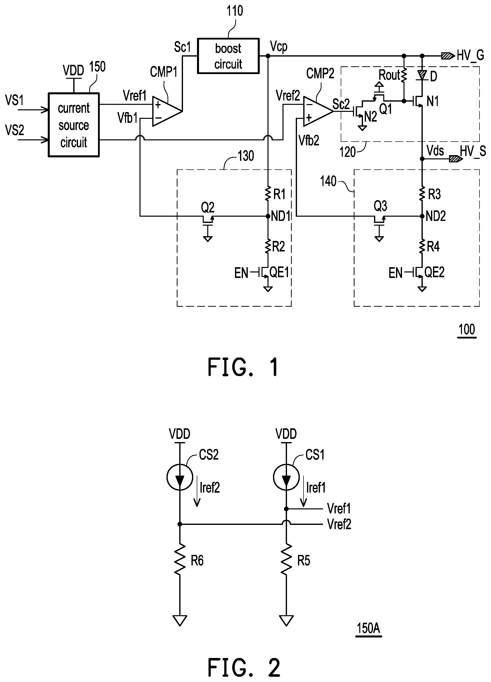
Please refer to , a voltage generating circuit 100 is adaptable for providing stable voltages to semiconductor memory devices such as NAND-type or NOR-type flash memories for performing reading, programming and erasing operations, including the step voltage used in the ISPP and ISPE operations. The voltage generating circuit 100 includes a first comparator CMP 1 , a second comparator CMP 2 , a boost circuit 110 , an output circuit 120 , a first feedback circuit 130 , a second feedback circuit 140 and a current source circuit 150 .
The non-inverting input terminal of the first comparator CMP 1 receives the first reference voltage Vref 1 , and the inverting input terminal receives the first feedback voltage Vfb 1 generated based on the first output node HV_G. The first comparator CMP 1 serves to compare the first reference voltage Vref 1 and the first feedback voltage Vfb 1 , and generate the first control signal Sc 1 according to the comparison result. For example, when the first reference voltage Vref 1 is greater than the first feedback voltage Vfb 1 , the first comparator CMP 1 generates the first control signal Sc 1 with a high logic level, and when the first reference voltage Vref 1 is lower than the first feedback voltage Vfb 1 , the first comparator CMP 1 generates the first control signal Sc 1 with a low logic level.
The boost circuit 110 is, for example, a charge pump, and is coupled to the first comparator CMP 1 and the first output node HV_G. The boost circuit 110 may be controlled by the first control signal Sc 1 to output the boost voltage Vcp to the first output node HV_G. For example, the boost circuit 110 may continuously increase the boost voltage Vcp in response to the first control signal Sc 1 at a high logic level until the first control signal Sc 1 turns to a low logic level.
The inverting input terminal of the second comparator CMP 2 receives the second reference voltage Vref 2 , and the non-inverting input terminal receives the second feedback voltage Vfb 2 generated based on the second output node HV_S. The second comparator CMP 2 serves to compare the second reference voltage Vref 2 and the second feedback voltage Vfb 2 , and generate the second control signal Sc 2 according to the comparison result. For example, when the second feedback voltage Vfb 2 is greater than the second reference voltage Vref 2 , the second comparator CMP 2 generates a second control signal Sc 2 of a high logic level, and when the second feedback voltage Vfb 2 is less than the second reference voltage Vref 2 , the second comparator CMP 2 generates a second control signal Sc 2 of a low logic level.
The output circuit 120 is coupled to the first output node HV_G, the second output node HV_S and the second comparator CMP 2 . The output circuit 120 receives the boost voltage Vcp, and is controlled by the second control signal Sc 2 to convert the boost voltage Vcp into a drive voltage Vds and output the drive voltage to the second output node HV_S. In terms of circuit structure, the output circuit 120 includes a diode D, a first N-type field effect transistor N 1 , an output resistor Rout, a second N-type field effect transistor N 2 and a first protection transistor Q 1 . The anode of the diode D is coupled to the first output node HV_G. The drain of the first N-type field effect transistor N 1 is coupled to the cathode of the diode D, and the source of the first N-type field effect transistor N 1 is coupled to the second output node HV_S. A first terminal of the output resistor Rout is coupled to the first output node HV_G, and a second terminal of the output resistor Rout is coupled to the gate of the first N-type field effect transistor N 1 . The source of the second N-type field effect transistor N 2 is coupled to the ground potential (0 volts), and the gate of the second N-type field effect transistor N 2 is coupled to the output terminal of the second comparator CMP 2 to receive the second control signal Sc 2 . The first terminal of the first protection transistor Q 1 is coupled to the drain of the second N-type field effect transistor N 2 , the second terminal is coupled to the gate of the first N-type field effect transistor N 1 , and the control terminal is coupled to the ground potential.
The first feedback circuit 130 is coupled to the inverting input terminal of the first comparator CMP 1 and the first output node HV_G. The first feedback circuit 130 may generate the first feedback voltage Vfb 1 to the inverting input terminal of the first comparator CMP 1 according to the boost voltage Vcp. In terms of circuit structure, the first feedback circuit 130 includes a first resistor R 1 , a second resistor R 2 , a first enable transistor QE 1 and a second protection transistor Q 2 . The first resistor R 1 is coupled between the first output node HV_G and the first feedback node ND 1 . The second resistor R 2 is coupled between the first feedback node ND 1 and the ground potential. The first enable transistor QE 1 is connected in series with the second resistor R 2 on the circuit path between the first feedback node ND 1 and the ground potential, and is configured to be turned on or off according to the enable signal EN. The first terminal of the second protection transistor Q 2 is coupled to the first feedback node ND 1 , the second terminal is coupled to the inverting input terminal of the first comparator CMP 1 , and the control terminal is coupled to the ground potential.
The second feedback circuit 140 is coupled to the non-inverting input terminal of the second comparator CMP 2 and the second output node HV_S. The second feedback circuit 140 may generate a second feedback voltage Vfb 2 to the non-inverting input terminal of the second comparator CMP 2 according to the drive voltage Vds. In terms of circuit structure, the second feedback circuit 140 includes a third resistor R 3 , a fourth resistor R 4 , a second enable transistor QE 2 and a third protection transistor Q 3 . The third resistor R 3 is coupled between the second output node HV_S and the second feedback node ND 2 . The fourth resistor R 4 is coupled between the second feedback node ND 2 and the ground potential. The second enable transistor QE 2 is connected in series with the fourth resistor R 4 on the circuit path between the second feedback node ND 2 and the ground potential, and is configured to be turned on or off according to the enable signal EN. The first terminal of the third protection transistor Q 3 is coupled to the second feedback node ND 2 , the second terminal is coupled to the non-inverting input terminal of the second comparator CMP 2 , and the control terminal is coupled to the ground potential. The first protection transistor Q 1 , the second protection transistor Q 2 , and the third protection transistor Q 3 are basically in a normally on state, and may serve to protect other components.
The current source circuit 150 is coupled to the first comparator CMP 1 and the second comparator CMP 2 . The current source circuit 150 operates under the power supply voltage VDD, and may adjust the first reference voltage Vref 1 according to the first voltage generating code VS 1 and the second voltage generating code VS 2 , and adjust the second reference voltage Vref 2 according to the first voltage generating code VS 1 .
In this embodiment, the boost voltage Vcp is determined by the first reference voltage Vref 1 , and the drive voltage Vds is determined by the second reference voltage Vref 2 . When the voltage generating circuit 100 is activated, the first enable transistor QE 1 and the second enable transistor QE 2 will be turned on due to receiving the enable signal EN of a high logic level. According to a voltage divider circuit formed by the first resistor R 1 and the second resistor R 2 , the boost voltage Vcp may be expressed through the following formula (1):
Vcp = Vfb 1 * ( R 1 + R 2 ) / R 2 ( 1 )
The boost circuit 110 will continue to increase the boost voltage Vcp until the first control signal Sc 1 changes to a low logic level. Therefore, the boost voltage Vcp will enter a steady state when the first feedback voltage Vfb 1 is equal to the first reference voltage Vref 1 . At this stage, the boost voltage Vcp may be expressed through the following formula (2):
Vcp = Vref 1 * ( R 1 + R 2 ) / R 2 ( 2 )
Similarly, according to the voltage divider circuit formed by the third resistor R 3 and the fourth resistor R 4 , the drive voltage Vds may be represented by the following formula (3):
Vds = Vfb 2 * ( R 3 + R 4 ) / R 4 ( 3 )
In , when the second control signal Sc 2 is at a low logic level, the second N-type field effect transistor N 2 is turned off, and the first N-type field effect transistor N 1 is turned on. In this case, the drive voltage Vds will be changed along with the boost voltage Vcp until the second control signal Sc 2 turns to a high logic level to turn on the second N-type field effect transistor N 2 and turn off the first N-type field effect transistor N 1 . Therefore, the drive voltage Vds enters a steady state when the second feedback voltage Vfb 2 is equal to the second reference voltage Vref 2 . At this stage, the drive voltage Vds may be expressed through the following formula (4):
Vds = Vref 2 * ( R 3 + R 4 ) / R 4 ( 4 )
As shown in the above formula (2) and formula (4), through the circuit structure of the voltage generating circuit 100 of the embodiment of the present disclosure, the boost voltage Vcp may be adjusted according to the first reference voltage Vref 1 , and the boost voltage Vcp may be adjusted according to the second reference voltage Vref 2 , and the voltage difference between the first output node HV_G and the second output node HV_S may be controlled separately. In this way, the boost voltage Vcp and the drive voltage Vds may be generated precisely while reducing the use of high-voltage components (such as potentiometers) for the semiconductor memory device to perform various operations.
In practical applications, the first resistor R 1 and the third resistor R 3 may adopt 114 k ohms, and the second resistor R 2 and the fourth resistor R 4 may adopt 6 k ohms. However, those skilled in the art may make appropriate adjustments depending on their actual needs.
The following examples illustrate the implementation details of the current source circuit. Please refer to and at the same time. The current source circuit 150 A includes a first current source CS 1 , a second current source CS 2 , a fifth resistor R 5 and a sixth resistor R 6 . A first terminal of the first current source CS 1 is coupled to the power supply voltage VDD, and a second terminal is coupled to the non-inverting input terminal of the first comparator CMP 1 . A first terminal of the fifth resistor R 5 is coupled to the second terminal of the first current source CS 1 , and the second terminal is coupled to the ground potential. A first terminal of the second current source CS 2 is coupled to the power supply voltage VDD, and a second terminal is coupled to the inverting input terminal of the second comparator CMP 2 . The first terminal of the sixth resistor R 6 is coupled to the second terminal of the second current source CS 2 , and the second terminal is coupled to the ground potential. The first current source CS 1 is configured to generate a first reference current Iref 1 according to the first voltage generating code VS 1 and the second voltage generating code VS 2 to provide the first reference voltage Vref 1 to the non-inverting input terminal of the first comparator CMP 1 . At this stage, the boost voltage Vcp may be expressed by the following formula (5):
Vcp = Iref 1 * R 5 * ( R 1 + R 2 ) / R 2 ( 5 )
The second current source CS 2 is configured to generate a second reference current Iref 2 according to the first voltage generating code VS 1 to provide a second reference voltage Vref 2 to the inverting input terminal of the second comparator CMP 2 . At this stage, the drive voltage Vds may be expressed through the following formula (6):
Vds = Iref 2 * R 6 * ( R 3 + R 4 ) / R 4 ( 6 )
In practical applications, the fifth resistor R 5 and the sixth resistor R 6 may adopt 100 k ohms, but those skilled in the art may make appropriate adjustments according to their actual needs.
Another embodiment is given below to illustrate the implementation details of the current source circuit. Please refer to and at the same time. The current source circuit 150 B includes a bias voltage circuit 300 , a trimming current generating circuit 310 , a basic current generating circuit 320 , an overdrive current generating circuit 330 and a current mirror circuit 340 . The bias circuit 300 is configured to generate a bias current Ibias (which is, for example, 4 microamperes).
The trimming current generating circuit 310 is coupled to the bias circuit 300 . The trimming current generating circuit 310 may generate multiple weighted currents Iw 1 ˜Iw 6 in a binary weighted incremental manner based on the bias current Ibias, and select the currents to be summed from the weighted currents Iw 1 ˜Iw 6 according to the first voltage generating code VS 1 , so as to generate trimming current Itrim. The current values of the weighted currents Iw 1 ˜Iw 6 are increased in binary weighting from low to high based on the mirror ratio of the transistors in the circuit. For example, the weighted current Iw 1 is 0.1 microamperes, the weighted current Iw 2 is 0.2 microamperes, the weighted current Iw 3 is 0.4 microamperes, the weighted current Iw 4 is 0.8 microamperes, the weighted current Iw 5 is 1.6 microamperes, and the weighted current Iw 6 is 3.2 microamperes.
The basic current generating circuit 320 is coupled to the bias circuit 300 and the trimming current generating circuit 310 . The basic current generating circuit 320 is configured to generate the basic current Ib. The basic current Ib is provided to generate the lowest drive voltage Vds, for example, 5.7 microamperes.
The overdrive current generating circuit 330 is coupled to the bias circuit 300 . The overdrive current generating circuit 330 may generate the overdrive current Iov according to the second voltage generating code VS 2 . The overdrive current Iov may be used to determine the voltage difference between the boost voltage Vcp and the drive voltage Vds.
The current mirror circuit 340 is coupled to the bias voltage circuit 300 , the trimming current generating circuit 310 , the basic current generating circuit 320 and the overdrive current generating circuit 330 . The current mirror circuit 340 may sum up the trimming current Itrim, the basic current Ib and the overdrive current Iov to generate the first reference current Iref 1 , so as to provide the first reference voltage Vref 1 to the non-inverting input terminal of the first comparator CMP 1 . Moreover, the trimming current Itrim and the basic current Ib may be summed up to generate a second reference current Iref 2 to provide a second reference voltage Vref 2 to the inverting input terminal of the second comparator CMP 2 . In other words, the first reference current Iref 1 is equal to the sum of the trimming current Itrim, the basic current Ib and the overdrive current Iov, and the second reference current Iref 2 is equal to the sum of the trimming current Itrim and the basic current Ib. Under the circumstances, the boost voltage Vcp may be expressed through the following formula (7), and the drive voltage Vds may be expressed through the following formula (8):
Vcp = ( Ib + Itrim + Iov ) * R 5 * ( R 1 + R 2 ) / R 2 ( 7 ) Vds = ( Ib + Itrim ) * R 6 * ( R 3 + R 4 ) / R 4 ( 8 )
In terms of circuit structure, the current mirror circuit 340 includes a third enable transistor QE 3 , first to eleventh P-type field effect transistors P 1 ˜P 11 , a third N-type field effect transistor N 3 , a fourth N-type field effect transistor N 4 , a fifth resistor R 5 and a sixth resistor R 6 . The first terminal of the third enable transistor QE 3 is coupled to the power supply voltage VDD, and the control terminal is coupled to the reverse enable signal ENB. The source of the first P-type field effect transistor P 1 is coupled to the second terminal of the third enable transistor QE 3 . The source of the second P-type field effect transistor P 2 is coupled to the drain of the first P-type field effect transistor P 1 , and the drain of the second P-type field effect transistor P 2 is coupled to the gate of the first P-type field effect transistor P 1 , the trimming current generating circuit 310 and the basic current generating circuit 320 . The source of the third P-type field effect transistor is coupled to the second terminal of the third enable transistor QE 3 , and the gate of the third P-type field effect transistor is coupled to the gate of the first P-type field effect transistor P 1 . The source of the fourth P-type field effect transistor P 4 is coupled to the drain of the third P-type field effect transistor P 3 , and the drain of the fourth P-type field effect transistor P 4 is coupled to the reverse input terminal of the second comparator CMP 2 . The gate of the fourth P-type field effect transistor P 4 is coupled to the gate of the second P-type field effect transistor P 2 . The source of the fifth P-type field effect transistor P 5 is coupled to the second terminal of the third enable transistor QE 3 , and the gate of the fifth P-type field effect transistor P 5 is coupled to the gate of the first P-type field effect transistor P 1 . The source of the sixth P-type field effect transistor P 6 is coupled to the drain of the fifth P-type field effect transistor P 5 , the drain of the sixth P-type field effect transistor P 6 is coupled to the non-inverting input terminal of the first comparator CMP 1 , and the gate of the sixth P-type field effect transistor P 6 is coupled to the gate of the second P-type field effect transistor P 2 . The source of the seventh P-type field effect transistor P 7 is coupled to the second terminal of the third enable transistor QE 3 . The source of the eighth P-type field effect transistor P 8 is coupled to the drain of the seventh P-type field effect transistor P 7 , the drain of the eighth P-type field effect transistor P 8 is coupled to the drain of the sixth P-type field effect transistor P 6 , and the gate of the eighth P-type field effect transistor P 8 is coupled to the gate of the second P-type field effect transistor P 2 . The source of the ninth P-type field effect transistor P 9 is coupled to the second terminal of the third enable transistor QE 3 , and the gate of the ninth P-type field effect transistor P 9 is coupled to the gate of the seventh P-type field effect transistor P 7 . The source of the tenth P-type field effect transistor P 10 is coupled to the drain of the ninth P-type field effect transistor P 9 , the drain of the tenth P-type field effect transistor P 10 is coupled to the gate of the ninth P-type field effect transistor P 9 and the overdrive current generating circuit 330 , and the gate of the tenth P-type field effect transistor P 10 is coupled to the gate of the second P-type field effect transistor P 2 . The source of the eleventh P-type field effect transistor P 11 is coupled to the power supply voltage VDD, and the drain and gate of the eleventh P-type field effect transistor P 11 are jointly coupled to the gate of the second P-type field effect transistor P 2 . The drain of the third N-type field effect transistor N 3 is coupled to the drain of the eleventh P-type field effect transistor P 11 , and the gate of the third N-type field effect transistor N 3 is coupled to the bias circuit 300 . The drain of the fourth N-type field effect transistor N 4 is coupled to the source of the third N-type field effect transistor N 3 , the source of the fourth N-type field effect transistor N 4 is coupled to the ground potential, and the gate of the fourth N-type field effect transistor N 4 is coupled to the bias circuit 300 . The first terminal of the fifth resistor R 5 is coupled to the drain of the sixth P-type field effect transistor P 6 , and the second terminal is coupled to the ground potential. The first terminal of the sixth resistor R 6 is coupled to the drain of the fourth P-type field effect transistor P 4 , and the second terminal is coupled to the ground potential.
The bias circuit 300 includes a third current source CS 3 , a fifth N-type field effect transistor N 5 , a fourth current source CS 4 , a sixth N-type field effect transistor N 6 , a seventh N-type field effect transistor N 7 , a fourth enable transistor QE 4 and a fifth enable transistor QE 5 . A first terminal of the third current source CS 3 is coupled to the power supply voltage VDD. The drain and gate of the fifth N-type field effect transistor N 5 are jointly coupled to the second terminal of the third current source CS 3 and the gate of the third N-type field effect transistor N 3 in the current mirror circuit 340 , and the source of the fifth N-type field effect transistor N 5 is coupled to the ground potential. The first terminal of the fourth current source CS 4 is coupled to the power supply voltage VDD. The drain of the sixth N-type field effect transistor N 6 is coupled to the second terminal of the fourth current source CS 4 , and the gate of the sixth N-type field effect transistor N 6 is coupled to the gate of the third N-type field effect transistor N 3 . The drain of the seventh N-type field effect transistor N 7 is coupled to the source of the sixth N-type field effect transistor N 6 , the gate of the seventh N-type field effect transistor N 7 is coupled to the drain of the sixth N-type field effect transistor N 6 and the gate of the fourth N-type field effect transistor N 4 in the current mirror circuit 340 , and the source of the seventh N-type field effect transistor N 7 is coupled to the ground potential. The first terminal of the fourth enable transistor QE 4 is coupled to the drain of the fifth N-type field effect transistor N 5 , the second terminal is coupled to the ground potential, and the control terminal is coupled to the reverse enable signal ENB. The first terminal of the fifth enable transistor QE 5 is coupled to the drain of the sixth N-type field effect transistor N 6 , the second terminal is coupled to the ground potential, and the control terminal is coupled to the reverse enable signal ENB.
The trimming current generating circuit 310 includes eighth to twenty-seventh N-type field effect transistors N 8 ˜N 27 . The drain of the eighth N-type field effect transistor N 8 is coupled to the drain of the second P-type field effect transistor P 2 in the current mirror circuit 340 , and the gate of the eighth N-type field effect transistor N 8 is coupled to the first encoding signal TR 1 . The drain of the ninth N-type field effect transistor N 9 is coupled to the source of the eighth N-type field effect transistor N 8 . The drain of the tenth N-type field effect transistor N 10 is coupled to the source of the ninth N-type field effect transistor N 9 , and the gate of the tenth N-type field effect transistor N 10 is coupled to the gate of the ninth N-type field effect transistor N 9 and the gate of the sixth N-type field effect transistor in the bias circuit 300 . The drain of the eleventh N-type field effect transistor N 11 is coupled to the source of the tenth N-type field effect transistor N 10 . The drain of the twelfth N-type field effect transistor N 12 is coupled to the source of the eleventh N-type field effect transistor N 11 , the source of the twelfth N-type field effect transistor N 12 is coupled to the ground potential, and the gate of the twelfth N-type field effect transistor N 12 is coupled to the gate of the eleventh N-type field effect transistor N 11 and the gate of the seventh N-type field effect transistor N 7 in the bias circuit 300 . The drain of the thirteenth N-type field effect transistor N 13 is coupled to the drain of the second P-type field effect transistor P 2 , and the gate of the thirteenth N-type field effect transistor N 13 is coupled to the second encoding signal TR 2 . The drain of the fourteenth N-type field effect transistor N 14 is coupled to the source of the thirteenth N-type field effect transistor N 13 , and the gate of the fourteenth N-type field effect transistor N 14 is coupled to the gate of the sixth N-type field effect transistor N 6 . The drain of the fifteenth N-type field effect transistor N 15 is coupled to the source of the fourteenth N-type field effect transistor N 14 , the source of the fifteenth N-type field effect transistor N 15 is coupled to ground potential, and the gate of the fifteenth N-type field effect transistor N 15 is coupled to the gate of the seventh N-type field effect transistor N 7 . The drain of the sixteenth N-type field effect transistor N 16 is coupled to the drain of the second P-type field effect transistor P 2 , and the gate of the sixteenth N-type field effect transistor N 16 is coupled to the third encoding signal TR 3 . The drain of the seventeenth N-type field effect transistor N 17 is coupled to the source of the sixteenth N-type field effect transistor N 16 , and the gate of the seventeenth N-type field effect transistor N 17 is coupled to the gate of the sixth N-type field effect transistor. The drain of the eighteenth N-type field effect transistor N 18 is coupled to the source of the seventeenth N-type field effect transistor N 17 , the source of the eighteenth N-type field effect transistor N 18 is coupled to the ground potential, and the gate of the eighteenth N-type field effect transistor N 18 is coupled to the gate of the seventh N-type field effect transistor N 7 . The drain of the nineteenth N-type field effect transistor N 19 is coupled to the drain of the second P-type field effect transistor P 2 , and the gate of the nineteenth N-type field effect transistor N 19 is coupled to the fourth encoding signal TR 4 . The drain of the twentieth N-type field effect transistor N 20 is coupled to the source of the nineteenth N-type field effect transistor N 19 , and the gate of the twentieth N-type field effect transistor N 20 is coupled to the gate of the sixth N-type field effect transistor N 6 . The drain of the twenty-first N-type field effect transistor N 21 is coupled to the source of the twenty-first N-type field effect transistor N 20 , the source of the twenty-first N-type field effect transistor N 21 is coupled to the ground potential, and the gate of the twenty-first N-type field effect transistor N 21 is coupled to the gate of the seventh N-type field effect transistor N 7 . The drain of the twenty-second N-type field effect transistor N 22 is coupled to the drain of the second P-type field effect transistor P 2 of the twenty-second N-type field effect transistor N 22 , and the gate of the twenty-second N-type field effect transistor N 22 is coupled to the fifth encoding signal TR 5 . The drain of the twenty-third N-type field effect transistor N 23 is coupled to the source of the twenty-second N-type field effect transistor N 22 , and the gate of the twenty-third N-type field effect transistor N 23 is coupled to the gate of the sixth N-type field effect transistor N 6 . The drain of the twenty-fourth N-type field effect transistor N 24 is coupled to the source of the twenty-third N-type field effect transistor N 23 , the source of the twenty-fourth N-type field effect transistor N 24 is coupled to the ground potential, and the gate of the twenty-fourth N-type field effect transistor N 24 is coupled to the gate of the seventh N-type field effect transistor N 7 . The drain of the twenty-fifth N-type field effect transistor N 25 is coupled to the drain of the second P-type field effect transistor P 2 , and the gate of the twenty-fifth N-type field effect transistor N 25 is coupled to the sixth encoding signal TR 6 . The drain of the twenty-sixth N-type field effect transistor N 26 is coupled to the source of the twenty-fifth N-type field effect transistor N 25 , and the gate of the twenty-sixth N-type field effect transistor N 26 is coupled to the gate of the sixth N-type field effect transistor N 6 . The drain of the twenty-seventh N-type field effect transistor N 27 is coupled to the source of the twenty-sixth N-type field effect transistor N 26 , the source of the twenty-seventh N-type field effect transistor N 27 is coupled to the ground potential, and the gate of the twenty-seventh N-type field effect transistor N 27 is coupled to the gate of the seventh N-type field effect transistor N 7 .
The basic current generating circuit 320 includes a twenty-eighth N-type field effect transistor N 28 and a twenty-ninth N-type field effect transistor N 29 . The drain of the twenty-eighth N-type field effect transistor N 28 is coupled to the drain of the second P-type field effect transistor P 2 in the current mirror circuit 340 , and the gate of the twenty-eighth N-type field effect transistor N 28 is coupled to the gate of the sixth N-type field effect transistor N 6 in the bias circuit 300 . The drain of the twenty-ninth N-type field effect transistor N 29 is coupled to the source of the twenty-eighth N-type field effect transistor N 28 , the source of the twenty-ninth N-type field effect transistor N 29 is coupled to the ground potential, and the gate of the twenty-ninth N-type field effect transistor N 29 is coupled to the gate of the seventh N-type field effect transistor N 7 in the bias circuit 300 .
In operation, the logic level of the reverse enable signal ENB is complementary to the logic level of the enable signal EN. When the voltage generating circuit 100 is activated, the third enable transistor QE 3 will be turned on due to receiving the reverse enable signal ENB of the low logic level, and the fourth enable transistor QE 4 and the fifth enable transistor QE 5 will be turned off due to receiving the reverse enable signal ENB of the low logic level. In this way, after the fifth P-type field effect transistor P 5 , the sixth P-type field effect transistor P 6 , the seventh P-type field effect transistor P 7 , and the eighth P-type field effect transistor P 8 are connected in parallel as shown in , the first reference current Iref 1 formed by the sum of the trimming current Itrim, the basic current Ib and the overdrive current Iov will be generated on the circuit path formed by the above transistors P 5 ˜P 8 and the fifth resistor R 5 connected in series. The second reference current Iref 2 formed by the sum of the trimming current Itrim and the basic current Ib will be generated on the circuit path formed by the third P-type field effect transistor P 3 , the fourth P-type field effect transistor P 4 and the sixth resistor R 6 connected in series.
In addition, the six bits of the first voltage generating code VS 1 are, for example, respectively input to the gates of the eighth N-type field effect transistor N 8 , the thirteenth N-type field effect transistor N 13 , the sixteenth N-type field-effect transistor N 16 , the nineteenth N-type field-effect transistor N 19 , the twenty-second N-type field-effect transistor N 22 , and the twenty-fifth N-type field-effect transistor N 25 as the first to the sixth encoding signals TR 1 ˜TR 6 to control the on or off of these transistors. By combining the six bits of the first voltage generating code VS 1 , it is possible to set 64 trimming currents Itrim. In this way, the trimming current Itrim may be adjusted during ISPP and ISPE operations to generate appropriate boost voltage Vcp and the drive voltage Vds.
It is worth mentioning that the internal structure of the basic current generating circuit 320 may also be similar to that of the overdrive current generating circuit 330 , so that the overdrive current Iov is generated according to the second voltage generating code VS 2 , but the present disclosure is not limited thereto.
In summary, the voltage generating circuit of the present disclosure not only is able to reduce the occupied area, but is also able to effectively improve the precision of the output voltage while reducing the use of high-voltage components, thereby reducing production costs.
Figures (2)
Citations
This patent cites (17)
- US7253676
- US10726927
- US11074983
- US2005/0168263
- US2008/0054991
- US2008/0129377
- US2008/0304349
- US2012/0063244
- US2017/0076800
- US2023/0318450
- US101201638
- US105322786
- US106531221
- US105359049
- US110097911
- USI685839
- USI737290