Current Detection Circuit and Electronic Device
Abstract
A current detection circuit comprises a signal input terminal, a signal output terminal, a switch branch, a first current detection branch, and a second current detection branch. The switch branch is configured to block the current flowing from the signal output terminal to the signal input terminal when the switch branch is turned off. When the switch branch is conducting, the current flowing from the signal input terminal through the switch branch to the signal output terminal is the switch branch current comprising a first part linearly related to a first voltage difference, and a second part exponentially related to the first voltage difference. The first voltage difference is the voltage difference between the signal input terminal and the signal output terminal. The first current detection branch outputs a first detection current representing the first part. The second current detection branch outputs a second detection current representing the second part.
Claims (19)
1 . A current detection circuit comprising: a signal input terminal, a signal output terminal, a switch branch, a first current detection branch, and a second current detection branch, wherein: the switch branch and the first current detection branch are connected between the signal input terminal and the signal output terminal; the second current detection branch is connected to the signal input terminal and the first current detection branch; and the switch branch is configured to block the current flowing from the signal output terminal to the signal input terminal when the switch branch is turned off, and wherein: when the switch branch is conducting, the current flowing from the signal input terminal through the switch branch to the signal output terminal is a switch branch current comprising a first current linearly related to a first voltage difference and a second current exponentially related to the first voltage difference, and wherein: the first voltage difference is a voltage difference across the signal input terminal and the signal output terminal; the first current detection branch is configured to output a first detection current representing the first current; and the second current detection branch is configured to output a second detection current representing the second current.
Show 18 dependent claims
2 . The current detection circuit according to claim 1 , wherein: the current detection circuit further comprises a summation branch, and wherein the summation branch is connected to the first current detection branch and the second current detection branch and is configured to output a third detection current based on the first detection current and the second detection current, and wherein the third detection current is 1/K times the switch branch current, and K>1, and wherein K is a predetermined parameter derived from transistor sizes and resistance values.
3 . The current detection circuit according to claim 2 , wherein: the first detection current is equal to 1/K of the first current.
4 . The current detection circuit according to claim 3 , wherein: the first current detection branch comprises a first transistor, a first amplifier, and a second transistor, and wherein: the first transistor is connected to the signal input terminal, the first amplifier, and the switch branch, and is configured with an equivalent resistance K times an equivalent resistance of the switch branch; the first amplifier is connected to the first transistor, the second transistor, and the signal output terminal; and a combination of the first amplifier and the second transistor is configured to maintain a voltage at a common terminal of the first transistor and the first amplifier equal to a voltage at the signal output terminal, so that the current flowing through the channel of the first transistor is the first detection current; or the first current detection branch comprises a first resistor, the first amplifier, and the second transistor, and wherein: the first resistor is connected to the signal input terminal and the first amplifier and is configured with a resistance value K times the equivalent resistance of the switch branch; the first amplifier is connected to the second transistor and the first resistor; and the combination of the first amplifier and the second transistor is configured to maintain the voltage at the common terminal of the first resistor and the first amplifier equal to the voltage at the signal output terminal, so that the current flowing through the first resistor is the first detection current.
5 . The current detection circuit according to claim 4 , wherein: a second input terminal of the first amplifier is connected to the signal output terminal; an output terminal of the first amplifier is connected to the first terminal of the second transistor; and the second terminal of the second transistor is used to output the first detection current, and wherein: when the first current detection branch comprises the first transistor, the first terminal of the first transistor is connected to the switch branch, the third terminal of the first transistor is connected to the signal input terminal, and the second terminal of the first transistor is connected to a first input terminal of the first amplifier and the third terminal of the second transistor; and when the first current detection branch comprises the first resistor, the first terminal of the first resistor is connected to the first input terminal of the first amplifier and the third terminal of the second transistor, and the second terminal of the first resistor is connected to the signal input terminal.
6 . The current detection circuit according to claim 5 , wherein: when the first current detection branch comprises the first resistor, the first current detection branch further comprises a second resistor for temperature compensation, a third transistor, a second amplifier, a fourth transistor, and a current mirror unit, and wherein: a first terminal of the second resistor is connected to the second terminal of the second transistor and a first input terminal of the second amplifier; a second input terminal of the second amplifier is connected to a second terminal of the third transistor and a second terminal of the fourth transistor; the output terminal of the first amplifier is connected to a first terminal of the fourth transistor; a second terminal of the second resistor and a third terminal of the third transistor are both grounded; a third terminal of the fourth transistor is connected to a first terminal of the current mirror unit; and a second terminal of the current mirror unit is used to output the first detection current.
7 . The current detection circuit according to claim 1 , wherein: the current detection circuit further comprises a summation branch, and wherein the summation branch is connected to the first current detection branch and the second current detection branch and is configured to output a third detection current based on the first detection current and the second detection current, and wherein the third detection current is 1/K times the switch branch current, and K>1, and wherein K is a predetermined parameter derived from transistor sizes and resistance values, and wherein the first detection current is equal to 1/K of the first current, and wherein: the first current detection branch comprises a fifth transistor, a third amplifier, a sixth transistor, and a first calibration unit, and wherein: the fifth transistor is connected to the signal input terminal, the third amplifier, and the switch branch; the third amplifier is also connected to the fifth transistor, the sixth transistor, and the signal output terminal, and a combination of the third amplifier and the sixth transistor is configured to maintain a voltage at a common terminal of the fifth transistor and the third amplifier equal to a voltage at the signal output terminal, so that a current flowing through a channel of the fifth transistor is linearly related to the first current; and the first calibration unit is connected to the sixth transistor and is configured to calibrate a current flowing through the sixth transistor to output the first detection current; or the first current detection branch comprises a third resistor, the third amplifier, the sixth transistor, and the first calibration unit, and wherein: the third resistor is connected to the signal input terminal and the third amplifier; a combination of the third amplifier and the sixth transistor is configured to maintain a voltage at a common terminal of the third resistor and the third amplifier equal to the voltage at the signal output terminal, so that the current flowing through the third resistor is linearly related to the first current; the first calibration unit is connected to the sixth transistor and is configured to calibrate the current flowing through the sixth transistor to output the first detection current.
8 . The current detection circuit according to claim 7 , wherein: a second input terminal of the third amplifier is connected to the signal output terminal; an output terminal of the third amplifier is connected to a first terminal of the sixth transistor; a second terminal of the sixth transistor is connected to a first terminal of the first calibration unit; and a second terminal of the first calibration unit is used to output the first detection current, and wherein: when the first current detection branch comprises the fifth transistor, a first terminal of the fifth transistor is connected to the switch branch, a third terminal of the fifth transistor is connected to the signal input terminal, and a second terminal of the fifth transistor is connected to a first input terminal of the third amplifier and a third terminal of the sixth transistor; and when the first current detection branch comprises the third resistor, a first terminal of the third resistor is connected to the first input terminal of the third amplifier and the third terminal of the sixth transistor, and a second terminal of the third resistor is connected to the signal input terminal.
9 . The current detection circuit according to claim 8 , wherein the first current detection branch further comprises a compensating resistor, and wherein: a first terminal of the compensating resistor is connected to the signal output terminal; a second terminal of the compensating resistor is connected to the second input terminal of the third amplifier and the third terminal of the first calibration unit; and the compensating resistor is configured such that a voltage-drop on the compensating resistor by a current output from the third terminal of the first calibration unit is equal to a voltage-drop on a connecting line, and wherein the connecting line is a connection between the switch branch and the signal output terminal.
10 . The current detection circuit according to claim 1 , wherein: the second detection current is equal to 1/K of the second current, and wherein K is a predetermined parameter derived from transistor sizes and resistance values.
11 . The current detection circuit according to claim 10 , wherein the second current detection branch comprises a seventh transistor, a fourth amplifier and an eighth transistor, and wherein: the seventh transistor is connected to the signal input terminal, and the seventh transistor is configured such that a body diode of the seventh transistor and a body diode in the switch branch have the same diode structure; the fourth amplifier is connected to the seventh transistor, the eighth transistor, and the signal output terminal; and a combination of the fourth amplifier and the eighth transistor is configured to maintain a voltage at a common terminal of the fourth amplifier and the seventh transistor equal to a voltage at the signal output terminal, so that a current flowing through the body diode of the seventh transistor is the second detection current.
12 . The current detection circuit according to claim 11 , wherein: a first terminal of the seventh transistor is connected to a second terminal of the seventh transistor, a first input terminal of the fourth amplifier, and a third terminal of the eighth transistor; a third terminal of the seventh transistor is connected to the signal input terminal; a second input terminal of the fourth amplifier is connected to the signal output terminal; an output terminal of the fourth amplifier is connected to a first terminal of the eighth transistor; and a second terminal of the eighth transistor is used to output the second detection current.
13 . The current detection circuit according to claim 1 , wherein the second detection current is equal to 1/K of the second current, and wherein K is a predetermined parameter derived from transistor sizes and resistance values, and wherein the second current detection branch comprises a ninth transistor, a fifth amplifier, a tenth transistor and a second calibration unit, and wherein: the ninth transistor is connected to the signal input terminal, and the ninth transistor is configured such that a body diode of the ninth transistor and a body diode in the switch branch have the same diode structure; the fifth amplifier is connected to the ninth transistor, the tenth transistor, and the signal output terminal; a combination of the fifth amplifier and the tenth transistor is configured to maintain a voltage at a common terminal of the fifth amplifier and the ninth transistor equal to a voltage at the signal output terminal, so that a current flowing through the body diode of the ninth transistor is linearly related to the second current; and the second calibration unit is connected to the tenth transistor, and the second calibration unit is configured to calibrate a current flowing through the tenth transistor to output the second detection current.
14 . The current detection circuit according to claim 13 , wherein: a first terminal of the ninth transistor is connected to a second terminal of the ninth transistor; the second terminal of the ninth transistor is connected to a first input terminal of the fifth amplifier and a third terminal of the tenth transistor; a second input terminal of the fifth amplifier is connected to the signal output terminal; an output terminal of the fifth amplifier is connected to a first terminal of the tenth transistor; a second terminal of the tenth transistor is connected to a first terminal of the second calibration unit; and a second terminal of the second calibration unit is used to output the second detection current.
15 . The current detection circuit according to claim 1 , wherein the first current detection branch comprises an eleventh transistor, a twelfth transistor, and a sixth amplifier, and wherein: the eleventh transistor is connected to the signal input terminal, the sixth amplifier, and the switch branch, and the eleventh transistor is configured such that an equivalent resistance of the eleventh transistor is K times an equivalent resistance of the switch branch; the sixth amplifier is connected to the eleventh transistor, the twelfth transistor, and the signal output terminal; a combination of the sixth amplifier and the twelfth transistor is configured to maintain a voltage at a common terminal of the eleventh transistor and the sixth amplifier equal to a voltage at the signal output terminal, so that a current flowing through a channel of the eleventh transistor is 1/K times the first current, and wherein K is a predetermined parameter derived from transistor sizes and resistance values.
16 . The current detection circuit according to claim 15 , wherein: a first terminal of the eleventh transistor is connected to the switch branch; a second terminal of the eleventh transistor is connected to a first input terminal of the sixth amplifier and a third terminal of the twelfth transistor; and a third terminal of the eleventh transistor is connected to the signal input terminal.
17 . The current detection circuit according to claim 16 , wherein the second current detection branch comprises a thirteenth transistor, and wherein: a first terminal of the thirteenth transistor is connected to both a second terminal of the thirteenth transistor and the first current detection branch; a third terminal of the thirteenth transistor is connected to the signal input terminal; and a current flowing through a body diode of the thirteenth transistor is the second detection current, and a sum of the second detection current and a current flowing through a body diode of the eleventh transistor is equal to 1/K times the second current.
18 . The current detection circuit according to claim 17 , wherein: a current flowing through the twelfth transistor is equal to 1/K times the switch branch current.
19 . The current detection circuit according to claim 1 , wherein the switch branch comprises a fourteenth transistor, and wherein: a second terminal and a cathode of a body diode of the fourteenth transistor are connected to the signal output terminal; a third terminal and an anode of the body diode of the fourteenth transistor are connected to the signal input terminal; the first current is a current flowing through a channel of the fourteenth transistor; and the second current is a current flowing through the body diode of the fourteenth transistor.
Full Description
Show full text →
RELATED APPLICATION
This application claims the benefit of and priority to Chinese Patent Application No. 2023106442438, filed on Jun. 2, 2023, which is hereby incorporated by reference in its entirety.
TECHNICAL FIELD
This application relates to the field of electronic circuit technology, particularly involving a current detection circuit and electronic device.
BACKGROUND
With the development of automotive electrification and intelligence, automotive chips are increasingly integrating monitoring, diagnosis, and protection functions. Power supply chips in automotive chips need to monitor the status of the load terminal and diagnose abnormal conditions at the load terminal.
For example, by monitoring the current at the load terminal, power supply chips can determine whether there is an overcurrent abnormal state at the load terminal. Furthermore, they can also cut off the power supply to the load terminal when the overcurrent abnormal state occurs to prevent the load from being damaged. Therefore, in order to protect the load in a timely manner, it is particularly important to accurately detect the current at the load terminal.
SUMMARY
This application aims to provide a current detection circuit and electronic device that can accurately detect the current flowing through a load.
To achieve the above objectives, in a first aspect, this application provides a current detection circuit comprising a signal input terminal, a signal output terminal, a switch branch, a first current detection branch, and a second current detection branch. The switch branch and the first current detection branch are both connected between the signal input terminal and the signal output terminal, and the second current detection branch is connected to the signal input terminal and the first current detection branch. The switch branch is configured to block the current flowing from the signal output terminal to the signal input terminal when the switch branch is turned off. When the switch branch is turned on, the current flowing from the signal input terminal through the switch branch to the signal output terminal is the switch branch current comprising a first current linearly related to the first voltage difference and a second current exponentially related to the first voltage difference, where a first voltage difference is the voltage difference between the signal input terminal and the signal output terminal.
The first current detection branch is configured to output a first detection current representing the first current. The second current detection branch is configured to output a second detection current representing the second current.
In an optional embodiment, the current detection circuit further includes a summation branch. The summation branch is connected to the first current detection branch and the second current detection branch and is configured to output a third detection current based on the first detection current and the second detection current, where the third detection current is 1/K times the switch branch current, and K>1.
In an optional embodiment, the first detection current is equal to 1/K of the first current.
In an optional embodiment, the first current detection branch comprises a first transistor, a first amplifier, and a second transistor. The first transistor is connected to the signal input terminal, the first amplifier and the switch branch. The first transistor is configured such that the equivalent internal resistance of the first transistor is K times the equivalent internal resistance of the switch branch.
The first amplifier is also connected to the first transistor, the second transistor, and the signal output terminal. The combination of the first amplifier and the second transistor is configured to maintain the voltage at the common terminal of the first transistor and the first amplifier equal to the voltage at the signal output terminal, such that the current flowing through the channel of the first transistor is the first detection current.
Alternatively, the first current detection branch comprises a first resistor, a first amplifier, and a second transistor. The first resistor is connected to the signal input terminal and the first amplifier. The first resistor is configured such that the resistance value of the first resistor is K times the equivalent internal resistance of the switch branch. The combination of the first amplifier and the second transistor is configured to maintain the voltage at the common terminal of the first resistor and the first amplifier equal to the voltage at the signal output terminal, such that the current flowing through the first resistor is the first detection current.
In an optional embodiment, the second input terminal of the first amplifier is connected to the signal output terminal. The output terminal of the first amplifier is connected to the first terminal of the second transistor, and the second terminal of the second transistor is used to output the first detection current. When the first current detection branch comprises the first transistor, the first terminal of the first transistor is connected to the switch branch. The third terminal of the first transistor is connected to the signal input terminal, and the second terminal of the first transistor is connected to the first input terminal of the first amplifier and the third terminal of the second transistor. When the first current detection branch comprises the first resistor, the first terminal of the first resistor is connected to the first input terminal of the first amplifier and the third terminal of the second transistor, and the second terminal of the first resistor is connected to the signal input terminal.
In an optional configuration, when the first current detection branch comprises the first resistor, the first current detection branch also comprises a second resistor for temperature compensation, a third transistor, a second amplifier, a fourth transistor, and a current mirror unit.
The first terminal of the second resistor is connected to the second terminal of the second transistor and the first input terminal of the second amplifier. The second input terminal of the second amplifier is connected to the second terminal of the third transistor and the second terminal of the fourth transistor. The output terminal of the second amplifier is connected to the first terminal of the fourth transistor. The second terminal of the second resistor and the third terminal of the third transistor are both grounded. The third terminal of the fourth transistor is connected to the first terminal of the current mirror unit, and the second terminal of the current mirror unit is used to output the first detection current.
In another optional configuration, the first current detection branch comprises a fifth transistor, a third amplifier, a sixth transistor, and a first calibration unit. The fifth transistor is connected to the signal input terminal, the third amplifier, and the switching branch. The third amplifier is also connected to the fifth transistor, the sixth transistor, and the signal output terminal. The combination of the third amplifier and the sixth transistor is configured to maintain the voltage at the common terminal of the fifth transistor and the third amplifier equal to the voltage at the signal output terminal, so that the current flowing through the channel of the fifth transistor is linearly related to the first current. The first calibration unit is connected to the sixth transistor and is configured to calibrate the current flowing through the sixth transistor to output the first detection current.
Alternatively, the first current detection branch comprises a third resistor, a third amplifier, a sixth transistor, and a first calibration unit. The third resistor is connected to the signal input terminal and the third amplifier. The combination of the third amplifier and the sixth transistor is configured to maintain the voltage at the common terminal of the third resistor and the third amplifier equal to the voltage at the signal output terminal, so that the current flowing through the third resistor is linearly related to the first current. The first calibration unit is connected to the sixth transistor and is configured to calibrate the current flowing through the sixth transistor to output the first detection current.
In an optional configuration, the second input terminal of the third amplifier is connected to the signal output terminal. The output terminal of the third amplifier is connected to the first terminal of the sixth transistor. The second terminal of the sixth transistor is connected to the first terminal of the first calibration unit, and the second terminal of the first calibration unit is used to output the first detection current. When the first current detection branch comprises the fifth transistor, the first terminal of the fifth transistor is connected to the switching branch. The third terminal of the fifth transistor is connected to the signal input terminal. The second terminal of the fifth transistor is connected to the first input terminal of the third amplifier and the third terminal of the sixth transistor. When the first current detection branch comprises the third resistor, the first terminal of the third resistor is connected to the first input terminal of the third amplifier and the third terminal of the sixth transistor. The second terminal of the third resistor is connected to the signal input terminal.
In an optional configuration, the first current detection branch also comprises a compensation resistor. The first terminal of the compensation resistor is connected to the signal output terminal. The second terminal of the compensation resistor is connected to the second input terminal of the third amplifier and the third terminal of the first calibration unit.
The compensation resistor is configured such that the voltage-drop across the compensation resistor formed by the current output from the third terminal of the first calibration unit is equal to the voltage-drop across a resistor on the first connection line, where the first connection line is the connection line between the switching branch and the signal output terminal.
In an optional configuration, the second detection current is equal to 1/K times the second current.
In an optional configuration, the second current detection branch comprises a seventh transistor, which is connected to the signal input terminal and is configured such that the body diode of the seventh transistor and the body diode in the switching branch have the same structure, a fourth amplifier and an eighth transistor, where the fourth amplifier is connected to the seventh transistor, the eighth transistor, and the signal output terminal. The combination of the fourth amplifier and the eighth transistor is configured to maintain the voltage at the common terminal of the fourth amplifier and the seventh transistor equal to the voltage at the signal output terminal, so that the current flowing through the body diode of the seventh transistor is the second detection current.
In an optional configuration, the first terminal of the seventh transistor is connected to the second terminal of the seventh transistor, the first input terminal of the fourth amplifier, and the third terminal of the eighth transistor. The third terminal of the seventh transistor is connected to the signal input terminal. The second input terminal of the fourth amplifier is connected to the signal output terminal. The output terminal of the fourth amplifier is connected to the first terminal of the eighth transistor. The second terminal of the eighth transistor is used to output the second detection current.
In an optional configuration, the second current detection branch comprises a ninth transistor, which is connected to the signal input terminal and is configured such that the body diode of the ninth transistor and the body diode in the switching branch have the same structure, a fifth amplifier and a tenth transistor, where the fifth amplifier is connected to the ninth transistor, the tenth transistor, and the signal output terminal. The combination of the fifth amplifier and the tenth transistor is configured to maintain the voltage at the common terminal of the fifth amplifier connected and the ninth transistor equal to the voltage at the signal output terminal, so that the current flowing through the body diode of the ninth transistor is linearly related to the second current, a second calibration unit, which is connected to the tenth transistor and is configured to calibrate the current flowing through the tenth transistor to output the second detection current.
In an optional configuration, the first terminal of the ninth transistor is connected to the second terminal of the ninth transistor. The second terminal of the ninth transistor is connected to the first input terminal of the fifth amplifier and the third terminal of the tenth transistor. The second input terminal of the fifth amplifier is connected to the signal output terminal. The output terminal of the fifth amplifier is connected to the first terminal of the tenth transistor. The second terminal of the tenth transistor is connected to the first terminal of the second calibration unit, and the second terminal of the second calibration unit is used to output the second detection current.
In an optional configuration, the first current detection branch comprises the eleventh transistor, the twelfth transistor, and the sixth amplifier. The eleventh transistor is connected to the signal input terminal, the sixth amplifier and the switching branch. The eleventh transistor is configured such that the equivalent resistance of the eleventh transistor is K times the equivalent resistance of the switching branch.
The sixth amplifier is also connected to the eleventh transistor, the twelfth transistor and the signal output terminal. The combination of the sixth amplifier and the twelfth transistor is configured to maintain the voltage at the common terminal of the sixth amplifier and the eleventh transistor equal to the voltage at the signal output terminal, so that the current flowing through the channel of the eleventh transistor is 1/K times the first current.
In an optional configuration, the first terminal of the eleventh transistor is connected to the switching branch. The second terminal of the eleventh transistor is connected to the first input terminal of the sixth amplifier and the third terminal of the twelfth transistor. The third terminal of the eleventh transistor is connected to the signal input terminal.
In an optional configuration, the second current detection branch comprises the thirteenth transistor. The first terminal of the thirteenth transistor is connected to the second terminal of the thirteenth transistor and the first current detection branch. The third terminal of the thirteenth transistor is connected to the signal input terminal. The current flowing through the body diode of the thirteenth transistor is the second detection current, and the second detection current plus the current flowing through the body diode of the eleventh transistor is equal to 1/K times the second current.
In an optional configuration, the current flowing through the twelfth transistor is 1/K times the current flowing through the switching branch.
In an optional configuration, the switching branch comprises the fourteenth transistor. The second terminal of the fourteenth transistor and the cathode of the body diode in the fourteenth transistor are both connected to the signal output terminal. The third terminal of the fourteenth transistor and the anode of the body diode in the fourteenth transistor are both connected to the signal input terminal. The first current is the current flowing through the channel of the fourteenth transistor, and the second current is the current flowing through the body diode of the fourteenth transistor.
Secondly, the present application provides an electronic device that comprises the current detection circuit as described above.
The advantageous effect of the present application is that the current detection circuit provided comprises a signal input terminal, a signal output terminal, a switching branch, a first current detection branch, and a second current detection branch. The switching branch and the first current detection branch are both connected between the signal input terminal and the signal output terminal, and the second current detection branch is connected to the signal input terminal and the first current detection branch. The switching branch is configured to block the current flowing from the signal output terminal to the signal input terminal when the switching branch is turned off. When the switching branch is conducting, the current flowing from the signal input terminal through the switching branch to the signal output terminal is the switching branch current, which comprises a first current linearly related to the first voltage difference and a second current exponentially related to the first voltage difference, where the first voltage difference is the voltage difference between the signal input terminal and the signal output terminal. The first current detection branch is configured to output a first detection current that represents the first current. The second current detection branch is configured to output a second detection current that represents the second current. Based on the first detection current and the second detection current, the detection of the switching branch current, which is the current flowing through the load, can be achieved, thereby accurately detecting the current flowing through the load.
The foregoing has outlined rather broadly the features and technical advantages of the present disclosure in order that the detailed description of the disclosure that follows may be better understood. Additional features and advantages of the disclosure will be described hereinafter which form the subject of the claims of the disclosure. It should be appreciated by those skilled in the art that the conception and specific embodiment disclosed may be readily utilized as a basis for modifying or designing other structures or processes for carrying out the same purposes of the present disclosure. It should also be realized by those skilled in the art that such equivalent constructions do not depart from the spirit and scope of the disclosure as set forth in the appended claims.
BRIEF DESCRIPTION OF THE DRAWINGS
For a more complete understanding of the present disclosure, and the advantages thereof, reference is now made to the following descriptions taken in conjunction with the accompanying drawings, in which:
One or more embodiments are exemplarily described with reference to the accompanying drawings, which are not intended to limit the embodiments. Elements in the drawings with the same reference numerals represent similar elements unless otherwise specified. The drawings are not to scale.
illustrates a schematic diagram of the structure of a current detection circuit provided in one embodiment of the present application;
illustrates a schematic diagram of the structure of a current detection circuit provided in another embodiment of the present application;
illustrates a circuit diagram of the current detection circuit provided in one embodiment of the present application;
illustrates a circuit diagram of the current detection circuit provided in a second embodiment of the present application;
illustrates a circuit diagram of the current detection circuit provided in a third embodiment of the present application;
illustrates a circuit diagram of the current detection circuit provided in a fourth embodiment of the present application;
illustrates a circuit diagram of the current detection circuit provided in a fifth embodiment of the present application;
illustrates a circuit diagram of the current detection circuit provided in a sixth embodiment of the present application;
illustrates a circuit diagram of the current detection circuit provided in a seventh embodiment of the present application;
illustrates a circuit diagram of the current detection circuit provided in an eighth embodiment of the present application;
illustrates a circuit diagram of the current detection circuit provided in a ninth embodiment of the present application;
illustrates a circuit diagram of the current detection circuit provided in a tenth embodiment of the present application; and
illustrates a circuit diagram of the current detection circuit provided in an eleventh embodiment of the present application.
Corresponding numerals and symbols in the different figures generally refer to corresponding parts unless otherwise indicated. The figures are drawn to clearly illustrate the relevant aspects of the various embodiments and are not necessarily drawn to scale.
DETAILED DESCRIPTION OF ILLUSTRATIVE EMBODIMENTS
The making and using of the presently preferred embodiments are discussed in detail below. It should be appreciated, however, that the present disclosure provides many applicable inventive concepts that can be embodied in a wide variety of specific contexts. The specific embodiments discussed are merely illustrative of specific ways to make and use the disclosure, and do not limit the scope of the disclosure.
In order to provide a clearer and more complete description of the objectives, technical solutions, and advantages of the embodiments described in this application, the following description, in conjunction with the accompanying drawings, will be used to describe the technical solutions in the embodiments of this application. It is evident that the described embodiments are part of the embodiments disclosed in this application, rather than the entirety of the embodiments. Based on the embodiments disclosed in this application, all other embodiments that ordinary skilled artisans can obtain without exercising inventive labor are within the scope of protection of this application.
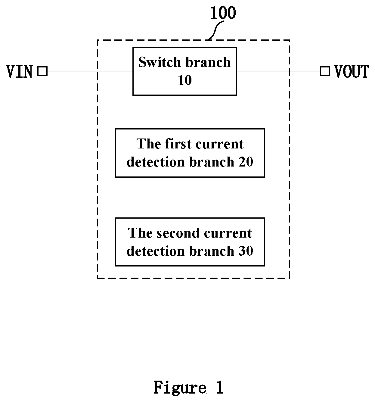
Please refer to , which illustrates a schematic diagram of the structure of a current detection circuit 100 provided in one embodiment of this application. As shown in , the current detection circuit 100 comprises a signal input terminal VIN, a signal output terminal VOUT, a switch branch 10 , a first current detection branch 20 , and a second current detection branch 30 .
The switch branch 10 and the first current detection branch 20 are both connected between the signal input terminal VIN and the signal output terminal VOUT, while the second current detection branch 30 is connected to the signal input terminal VIN and the first current detection branch 20 .
Specifically, the switch branch 10 is configured to block the current flowing from the signal output terminal VOUT to the signal input terminal VIN when the switch branch 10 is turned off. When the switch branch 10 is conducting, the current flowing from the signal input terminal VIN through the switch branch 10 to the signal output terminal VOUT is the switch branch current. The switch branch current comprises a first part of current that is linearly related to the first voltage difference, and a second part of current that is exponentially related to a first voltage difference, where the first voltage difference is the voltage difference between the signal input terminal VIN and the signal output terminal VOUT. The first current detection branch 20 is configured to output a first detection current I 1 that represents the first part of the switch branch current, while the second current detection branch 30 is configured to output a second detection current I 2 that represents the second part of the switch branch current.
Through the above approach, the switch branch current is divided into two different parts, and these two parts of current are processed separately to obtain the first detection current I 1 and the second detection current I 2 . Finally, based on the first detection current I 1 and the second detection current I 2 , the detection of the switch branch current, which corresponds to the detection of the current flowing into the load, can be accurately achieved.
In one embodiment, as shown in , the current detection circuit 100 further comprises a summation branch 40 . The summation branch 40 is connected to both the first current detection branch 20 and the second current detection branch 30 . The summation branch 40 is configured to output a third detection current based on the first detection current I 1 and the second detection current I 2 . The third detection current is equal to 1/K times the switch branch current, where K>1.
In some embodiments, the third detection current is obtained by summing the first detection current I 1 and the second detection current I 2 . By using the third detection current, the magnitude of the switch branch current can be determined. It should be noted that the summation branch 40 may not only simply add the first detection current I 1 and the second detection current I 2 , but also comprise a linear transformation of the first detection current I 1 and the second detection current I 2 before summing them to maintain a proportional relationship of 1/K between the third detection current and the switch branch current.
Please refer to , which exemplarily shows a circuit structure of the current detection circuit 100 . In one embodiment, as shown in , the switch branch 10 comprises a fourteenth transistor Q 14 . The second terminal of the fourteenth transistor Q 14 and the cathode of the body diode in the fourteenth transistor Q 14 are both connected to the signal output terminal VOUT. The third terminal of the fourteenth transistor Q 14 and the anode of the body diode in the fourteenth transistor Q 14 are both connected to the signal input terminal VIN.
One function of the fourteenth transistor Q 14 is to prevent a reverse flow of the current. When the fourteenth transistor Q 14 is controlled to be turned off, the body diode of the fourteenth transistor Q 14 can prevent the current from flowing back from the signal output terminal VOUT to the signal input terminal VIN. Another function of the fourteenth transistor Q 14 is that when the fourteenth transistor Q 14 is controlled to be conducting, the current flowing through the fourteenth transistor Q 14 from the signal input terminal VIN to the signal output terminal VOUT (i.e., the switch branch current) can be detected by the current detection circuit 100 .
The current flowing through the fourteenth transistor Q 14 is divided into two parts. The first part of the current is the current flowing through the channel of the fourteenth transistor Q 14 . When the fourteenth transistor Q 14 is conducting, the on-resistance of the fourteenth transistor Q 14 can be equivalent to a resistor. As such, this channel current is linearly related to the first voltage difference. The second part of current is the current flowing through the body diode D 14 of the fourteenth transistor Q 14 , and this current is exponentially related to the first voltage difference. When the first voltage difference is small, the second part of current flowing through the body diode D 14 of the fourteenth transistor Q 14 can be neglected. However, when the first voltage difference is large, continuing to neglect this second part of current will introduce significant errors in the current detection. The present invention aims to achieve higher current detection accuracy by separately detecting the first part of the current and the second part of the current through the construction of the first current detection branch and the second current detection branch.
In one embodiment, the first current detection branch 20 comprises a first resistor R 1 , a first amplifier U 1 , and a second transistor Q 2 . The first resistor R 1 is connected to both the signal input terminal VIN and the first amplifier U 1 . Specifically, the second input terminal of the first amplifier U 1 is connected to the signal output terminal VOUT. The output terminal of the first amplifier U 1 is connected to the first terminal of the second transistor Q 2 . The second terminal of the second transistor Q 2 is used to output the first detection current I 1 to the summation branch 40 . The first terminal of the first resistor R 1 is connected to the first input terminal of the first amplifier U 1 and the third terminal of the second transistor Q 2 . The second terminal of the first resistor R 1 is also connected to the signal input terminal VIN.
The first resistor R 1 is configured such that its resistance value is K times the equivalent resistance of the switch branch 10 . The combination of the first amplifier U 1 and the second transistor Q 2 is configured to maintain the voltage at the common terminal of the first resistor R 1 and the first amplifier U 1 (i.e., the voltage at the first terminal of the first resistor R 1 ) equal to the voltage at the signal output terminal VOUT, thereby causing the current flowing through the first resistor R 1 to be the first detection current I 1 .
In one embodiment, the second current detection branch 30 comprises a seventh transistor Q 7 , a fourth amplifier U 4 , and an eighth transistor Q 8 . The seventh transistor Q 7 is connected to the signal input terminal VIN, and the fourth amplifier U 4 is connected to the seventh transistor Q 7 , the eighth transistor Q 8 and the signal output terminal VOUT.
Specifically, the first terminal of the seventh transistor Q 7 is connected to the second terminal of the seventh transistor Q 7 , the first input terminal of the fourth amplifier U 4 , and the third terminal of the eighth transistor Q 8 . The third terminal of the seventh transistor Q 7 is connected to the signal input terminal VIN. The second input terminal of the fourth amplifier U 4 is connected to the signal output terminal VOUT. The output terminal of the fourth amplifier U 4 is connected to the first terminal of the eighth transistor Q 8 . The second terminal of the eighth transistor Q 8 is used to output the second detection current I 2 to the summation branch 40 .
In the embodiment, the seventh transistor Q 7 is configured such that the body diode D 7 of the seventh transistor Q 7 has the same structure as the body diode in the switch branch 10 . The combination of the fourth amplifier U 4 and the eighth transistor Q 8 is configured to maintain the voltage at the common terminal of the fourth amplifier U 4 and the seventh transistor Q 7 equal to the voltage at the signal output terminal VOUT, thereby causing the current flowing through the body diode D 7 of the seventh transistor Q 7 to be the second detection current I 2 .
It should be noted that in the embodiments of this application, MOS transistors are used as examples. The gate of the MOS transistor corresponds to the first terminal of the transistor. The source corresponds to the second terminal, and the drain corresponds to the third terminal.
For example, as shown in , the second transistor Q 2 is an NMOS transistor. The gate of the NMOS transistor corresponds to the first terminal of the second transistor Q 2 . The source corresponds to the second terminal, and the drain corresponds to the third terminal.
In addition, the transistors can be any controllable switches, such as insulated gate bipolar transistor (IGBT) devices, integrated gate-commutated thyristor (IGCT) devices, gate turn-off thyristor (GTO) devices, silicon-controlled rectifier (SCR) devices, junction field-effect transistor (JFET) devices, MOS-controlled thyristor (MCT) devices, etc.
The principle of the circuit structure shown in is explained below. In practical applications, the signal input terminal VIN is usually connected to the input power supply, and the signal output terminal VOUT is usually connected to the load. Therefore, when the fourteenth transistor Q 14 is conducting, the current flows from the signal input terminal VIN through the fourteenth transistor Q 14 and enters the load through the signal output terminal VOUT. This current entering the load is referred to as the switch branch current.
In the related art, when detecting the current flowing into the load, usually only the current flowing through the channel of the fourteenth transistor Q 14 is considered, while the current flowing through the body diode D 14 of the fourteenth transistor Q 14 is neglected. However, when the current flowing into the load is large, the voltage-drop across the channel resistance of the fourteenth transistor Q 14 increases, resulting in an increased voltage across the body diode D 14 and causing the body diode D 14 to conduct more fully. As a result, the current flowing through the body diode D 14 becomes significant, and neglecting this current will greatly reduce the detection accuracy.
In the embodiment of the present application, both the current flowing through the channel of the fourteenth transistor Q 14 (which is related to the equivalent internal resistance of the fourteenth transistor Q 14 ) and the current flowing through the body diode D 14 of the fourteenth transistor Q 14 are detected, thereby improving the detection accuracy. The specific detection process is as follows:
Regarding the current flowing through the channel of the fourteenth transistor Q 14 , which corresponds to the first part of the switch branch current, the following steps can be performed. Firstly, by utilizing the combination of the first amplifier U 1 and the second transistor Q 2 , the “virtual short” characteristic between the two input terminals of the operational amplifier can be used to configure the voltage at the first terminal of the first resistor R 1 to be equal to the voltage at the second terminal of the fourteenth transistor Q 14 . Secondly, the second terminal of the first resistor R 1 and the third terminal of the fourteenth transistor Q 14 are both connected to the signal input terminal VIN. Therefore, the voltage at the second terminal of the first resistor R 1 is also equal to the voltage at the third terminal of the fourteenth transistor Q 14 . In summary, the voltage across the two terminals of the first resistor R 1 is equal to the voltage between the second and third terminals of the fourteenth transistor Q 14 . At the same time, the resistance value of the first resistor R 1 is K times the equivalent internal resistance of the fourteenth transistor Q 14 . Hence, the current flowing through the first resistor R 1 corresponds to 1/K of the current flowing through the channel of the fourteenth transistor Q 14 . Due to the “virtual open” characteristic of the two input terminals of the operational amplifier, the current flowing through the first resistor R 1 is equivalent to the current flowing through the second transistor Q 2 , which is the first detection current I 1 . The first detection current I 1 represents the first part of the switch branch current as the first detection current I 1 is 1/K of the first part of the switch branch current.
Regarding the current flowing through the body diode D 14 of the fourteenth transistor Q 14 , which corresponds to the second part of the switch branch current, the following steps can be performed. Firstly, by short-circuiting the first terminal and the second terminal of the seventh transistor Q 7 , the seventh transistor Q 7 operates in the off state. At this time, the current flows from the signal input terminal VIN through the body diode D 7 of the seventh transistor Q 7 , the eighth transistor Q 8 , and enters the summing branch 40 . Secondly, by utilizing the combination of the fourth amplifier U 4 and the eighth transistor Q 8 , the “virtual short” characteristic between the two input terminals of the operational amplifier can be used to configure the voltage at the cathode of the body diode D 7 of the seventh transistor Q 7 to be equal to the voltage at the cathode of the body diode D 14 of the fourteenth transistor Q 14 . Furthermore, the anode of the body diode D 7 of the seventh transistor Q 7 and the anode of the body diode D 14 of the fourteenth transistor Q 14 are both connected to the signal input terminal VIN. Hence, the voltage at the anode of the body diode D 7 of the seventh transistor Q 7 is also equal to the voltage at the anode of the body diode D 14 of the fourteenth transistor Q 14 . In summary, the voltage across the two terminals of the body diode D 7 of the seventh transistor Q 7 is equal to the voltage across the two terminals of the body diode D 14 of the fourteenth transistor Q 14 .
When the diode is forward-biased, the current can be expressed as: I ( D )= Is ×( e VD/Vt −1)
In Equation above, Vt is the thermal voltage depending on temperature. Vt is approximately equal to 26 mV at room temperature, and Is is the reverse saturation current of the diode. It can be observed that the current flowing through the diode and the voltage difference VD across the diode terminals are exponentially related, meaning that the current flowing through the body diode D 14 of the fourteenth transistor Q 14 is exponentially related to the voltage difference between the signal input terminal VIN and the signal output terminal VOUT. Moreover, for diodes with the same structure, the reverse saturation current Is is proportional to the cross-sectional area of the diode.
Therefore, the body diode D 7 of the seventh transistor Q 7 and the body diode D 14 of the fourteenth transistor Q 14 can be configured as diodes with the same structure. As both the seventh transistor Q 7 and the fourteenth transistor Q 14 have transistor structures, with only a difference in size, the reverse saturation currents Is of the corresponding diodes are different. However, the currents flowing through the body diode D 7 of the seventh transistor Q 7 and the body diode D 14 of the fourteenth transistor Q 14 vary linearly with the voltage difference between their two terminals. Consequently, the current flowing through the body diode D 7 of the seventh transistor Q 7 can be configured as 1/K of the current flowing through the body diode D 14 of the fourteenth transistor Q 14 . According to the “virtual open” characteristic of the operational amplifier input terminals, the current flowing through the body diode D 7 of the seventh transistor Q 7 is equivalent to the current flowing through the eighth transistor Q 8 , which is the second detection current I 2 . The second detection current I 2 represents the second part of the switch branch current, as the second detection current I 2 is 1/K of the second part of the switch branch current.
The sum of the first part of the switch branch current and the second part of the switch branch current is K times the sum of the first detection current I 1 and the second detection current I 2 , which is the third detection current. The sum of the first part of the switch branch current and the second part of the switch branch current is also the total current flowing through the fourteenth transistor Q 14 (corresponding to the current flowing through the switch branch in the above embodiments), which is the current flowing into the load. Therefore, the third detection current is equal to 1/K of the current flowing into the load. By obtaining the third detection current, the current flowing into the load can be determined with high accuracy.
Specifically, taking the implementation of the current detection circuit shown in as an example, the seventh transistor Q 7 and the fourteenth transistor Q 14 are both PMOS transistors, while the second transistor Q 2 and the eighth transistor Q 8 are both NMOS transistors. Correspondingly, the first input terminals of the first amplifier U 1 and the second amplifier U 2 are configured as the in-phase input terminals of the respective amplifiers, and their second input terminals are configured as the inverted input terminals of the respective amplifiers.
It should be noted that the hardware structure of the current detection circuit 100 shown in is only an example. The current detection circuit 100 can have more or fewer components than those shown in the figure. Two or more components may be combined. The components may have different component configurations. The various components shown in the figure can be implemented in a combination of hardware, software, or hardware and software, including one or more signal processing and/or dedicated integrated circuits.
For example, in one embodiment shown in , the first current detection branch 20 further comprises a second resistor R 2 , a third transistor Q 3 , a second amplifier U 2 , a fourth transistor Q 4 , and a current mirror unit 21 for temperature compensation.
The first terminal of the second resistor R 2 is connected to the second terminal of the second transistor Q 2 and the first input terminal of the second amplifier U 2 . The second input terminals of the second amplifier U 2 are connected to the second terminal of the third transistor Q 3 and the second terminal of the fourth transistor Q 4 . The output terminal of the second amplifier U 2 is connected to the first terminal of the fourth transistor Q 4 . The second terminal of the second resistor R 2 and the third terminal of the third transistor Q 3 are both grounded. The third terminal of the fourth transistor Q 4 is connected to the first terminal of the current mirror unit 21 . The second terminal of the current mirror unit 21 is used to output the first detection current I 1 .
In this embodiment, the resistances of resistors and the on-resistances of the transistors usually have different temperature coefficients (i.e., the resistance of the first resistor R 1 and the on-resistance of the fourteenth transistor Q 14 usually have different temperature coefficients). Therefore, it is necessary to compensate for the temperature coefficient difference to more accurately control the current through the first resistor R 1 as 1/K of the current flowing through the channel of the fourteenth transistor Q 14 . Specifically, the temperature coefficient difference between the resistance of the first resistor R 1 and the on-resistance of the fourteenth transistor Q 14 can be compensated by the second resistor R 2 , the third transistor Q 3 , the second amplifier U 2 , the fourth transistor Q 4 , and the current mirror unit 21 . The second resistor R 2 is of the same type as the first resistor R 1 , and the third transistor Q 3 is of the same type as the fourteenth transistor Q 14 . Ideally, the voltage value of the reference remains constant regardless of temperature. The second amplifier U 2 generates a current flowing through the third transistor Q 3 , which is mirrored by the current mirror unit 21 to produce the first detection current I 1 .
Specifically, the current IQ 3 flowing through the third transistor Q 3 and the fourth transistor Q 14 can be expressed as:
IQ 3 = IC 14 × ( R 2 / R 1 ) × ( RQ 14 RQ 3 )
In Equation above, IC 14 represents the current flowing through the channel of the fourteenth transistor, which is the first part of the switch branch current. R 1 and R 2 represent the resistance values of the first resistor R 1 and the second resistor R 2 , respectively. RQ 3 and RQ 14 represent the on-resistance of the third transistor Q 3 and the on-resistance of the fourteenth transistor Q 14 , respectively. From the equation, it can be seen that the relationship between IQ 3 and the first part of the switch branch current is determined by the ratio of the resistance values of the first resistor R 1 and the second resistor R 2 , and the ratio of the on-resistance of the third transistor Q 3 and the on-resistance of the fourteenth transistor Q 14 . The relationship is not determined solely by the resistance values or on-resistance of any transistor or resistor. This configuration can effectively compensate for the influence of the temperature coefficient of the resistance and transistor on-resistance on the current ratio.
In some embodiments, the voltage difference between the first terminal and the second terminal of the third transistor Q 3 needs to be kept the same as the voltage difference between the first terminal and the second terminal of the fourteenth transistor Q 14 to maintain a stable ratio between the on-resistance of the third transistor Q 3 and the on-resistance of the fourteenth transistor Q 14 . In practical applications, the voltage at the first terminal of the fourteenth transistor Q 14 is the voltage between the first terminal and the second terminal of the fourteenth transistor Q 14 plus the voltage at the signal output terminal VOUT. At this time, the voltage at the first terminal of the third transistor Q 3 is the voltage at the first terminal of the fourteenth transistor Q 14 minus the superimposed part (i.e., the voltage at the signal output terminal VOUT).
Understandably, the circuit structure shown in aims to add a partial circuit for temperature compensation to eliminate errors that may arise from the temperature coefficient difference between the resistor and the on-resistance of the transistor. As for the part related to detecting the current flowing into the load, it is similar to the circuit structure shown in . Please refer to the detailed description of for details, which will not be repeated herein.
Please refer to . shows another structural example of the first current detection branch 20 . As shown in , the first current detection branch 20 comprises a third resistor R 3 , a third amplifier U 3 , a sixth transistor Q 6 , and a first calibration unit 22 . The third resistor R 3 is connected to the signal input terminal VIN and the third amplifier U 3 . The first calibration unit 22 is connected to the sixth transistor Q 6 . Specifically, the second input terminal of the third amplifier U 3 is connected to the signal output terminal VOUT. The output terminal of the third amplifier U 3 is connected to the first terminal of the sixth transistor Q 6 . The second terminal of the sixth transistor Q 6 is connected to the first terminal of the first calibration unit 22 . The second terminal of the first calibration unit 22 is used to output the first detection current I 1 . The first terminal of the third resistor R 3 is connected to the first input terminal of the third amplifier U 3 and the third terminal of the sixth transistor Q 6 . The second terminal of the third resistor R 3 is connected to the signal input terminal VIN.
In this embodiment, the combination of the third amplifier U 3 and the sixth transistor Q 6 is configured to maintain the voltage at the common terminal of the third resistor R 3 and the third amplifier U 3 equal to the voltage at the signal output terminal VOUT, so that the current flowing through the third resistor R 3 is linearly related to the first part of the switch branch current. The first calibration unit 22 is configured to calibrate the current flowing through the sixth transistor Q 6 in order to output the first detection current I 1 .
This embodiment differs from the circuit structure shown in . In particular, the first calibration unit 22 is added. As a result, it is not necessary to precisely achieve the resistance value of the first resistor R 1 as K times the equivalent on-resistance of the fourteenth transistor Q 14 . Because the first calibration unit 22 can calibrate the gain and offset of the first current detection branch 20 , which means the current entering the first calibration unit 22 does not have to be exactly 1/K of the current flowing through the channel of the fourteenth transistor Q 14 , the first calibration unit 22 adjusts it (i.e., the current entering the first calibration unit 22 ) to be 1/K of the current flowing through the channel of the fourteenth transistor Q 14 . In this embodiment, since it is not necessary to precisely achieve the resistance value of the first resistor R 1 as K times the equivalent on-resistance of the fourteenth transistor Q 14 , it is easier to achieve in practical engineering and has higher practicality.
For example, the second resistor R 2 , the second amplifier U 2 , the third transistor Q 3 , the fourth transistor Q 4 , and the current mirror unit 21 in the temperature compensation unit shown in can be considered as a specific implementation of the first calibration unit 22 shown in .
In one embodiment, as shown in , the first current detection branch 20 further adds a compensating resistor R 4 based on the structure in . The first terminal of the compensating resistor R 4 is connected to the signal output terminal VOUT, and the second terminal of the compensating resistor R 4 is connected to the second input terminal of the third amplifier U 3 and the third terminal of the first calibration unit 22 .
Specifically, the compensating resistor R 4 is configured to have a voltage-drop formed by the current I 3 output from the third terminal of the first calibration unit 22 equal to the voltage-drop across the first connecting line resistor. Here, the first connecting line refers to the connecting line between the switch branch 10 and the signal output terminal VOUT.
In this embodiment, the resistor (represented as the fourteenth resistor R 14 in ) between the second terminal of the fourteenth transistor Q 14 and the signal output terminal VOUT (i.e., the first connection line) affects the accuracy of current detection. Therefore, by setting a compensating resistor R 4 and utilizing the current I 3 output from the third terminal of the first calibration unit 22 , a voltage-drop (referred to as the first voltage-drop V 1 ) is generated across the compensating resistor R 4 . The voltage-drop across the two terminals of the fourteenth resistor R 14 (i.e., the voltage-drop across the resistor on the first connection line, referred to as the second voltage-drop V 2 ) is equal in magnitude to the first voltage-drop V 1 . The first voltage-drop V 1 and the second voltage-drop V 2 cancel each other out, thereby compensating for the voltage-drop across the resistor on the first connection line and improving the accuracy of current detection. Please refer to , which illustrates another structure of the first current detection branch 20 . As shown in , the first current detection branch 20 comprises the first transistor Q 1 , the first amplifier U 1 , and the second transistor Q 2 .
The first transistor Q 1 is connected to the signal input terminal VIN, the first amplifier U 1 , and the switch branch 10 . The first amplifier U 1 is also connected to the first transistor Q 1 , the second transistor Q 2 , and the signal output terminal VOUT.
Specifically, the second input terminal of the first amplifier U 1 is connected to the signal output terminal VOUT. The output terminal of the first amplifier U 1 is connected to the first terminal of the second transistor Q 2 . The second terminal of the second transistor Q 2 is used to output the first detection current I 1 . The first terminal of the first transistor Q 1 is connected to the first terminal of the fourteenth transistor Q 14 . The third terminal of the first transistor Q 1 is connected to the signal input terminal VIN. The second terminal of the first transistor Q 1 is connected to the first input terminal of the first amplifier U 1 and the third terminal of the second transistor Q 2 .
In this embodiment, the first transistor Q 1 is configured such that its equivalent on-resistance is K times the equivalent on-resistance of the switch branch 10 . The combination of the first amplifier U 1 and the second transistor Q 2 is configured to maintain the voltage at the terminal of the first transistor Q 1 connected to the first amplifier U 1 equal to the voltage at the signal output terminal VOUT, so that the current flowing through the channel of the first transistor Q 1 is the first detection current I 1 .
Specifically, the structure shown in differs from the structure shown in in that the first resistor R 1 is replaced by the first transistor Q 1 , and the equivalent on-resistance of the first transistor Q 1 serves the same purpose as the first resistor R 1 . Therefore, in this embodiment, the first transistor Q 1 can be viewed as a resistor with a resistance value equal to the equivalent on-resistance of the first transistor Q 1 . Subsequently, the process of detecting the current flowing into the load is similar to the circuit structure shown in , within the understanding of those skilled in the art, and will not be further elaborated herein.
It is worth pointing out that, in most configurations, the first transistor Q 1 in also has a body diode. According to previous analysis, the body diode of the first transistor Q 1 would have the same voltage across its two terminals as the body diode of the fourteenth transistor Q 14 . In this case, it may also carry current when the fourteens transistor Q 14 is turned on. However, due to process and transistor layout limitations, it is very difficult to design a first transistor Q 1 such that the ratio between the current flowing through its channel and the first portion of the switch branch current is the same as the ratio between the current flowing through its body diode and the second portion of the switch branch current. Such that a dedicated second current detection branch comprising diode connected seventh transistor Q 7 is always required to achieve high accuracy current detection.
Additionally, in this embodiment, it is only necessary to configure the first transistor Q 1 and the fourteenth transistor Q 14 as the same type of transistors with similar temperature characteristics. Therefore, there is no need to set up additional circuitry for temperature compensation. Moreover, since the first transistor Q 1 and the fourteenth transistor Q 14 have similar structures, the specific ratio of their width-to-length ratios can be configured to achieve a specific ratio of equivalent on-resistances.
It should be understood that similar technical features added in or 6 are also applicable to the circuit structure shown in . For example, in one embodiment, as shown in , the first current detection branch 20 comprises the fifth transistor Q 5 , the third amplifier U 3 , the sixth transistor Q 6 , and the first calibration unit 22 . The fifth transistor Q 5 is connected to the signal input terminal VIN, the third amplifier U 3 , and the switch branch 10 . The third amplifier U 3 is also connected to the fifth transistor Q 5 , the sixth transistor Q 6 , and the signal output terminal VOUT.
Specifically, the second input terminal of the third amplifier U 3 is connected to the signal output terminal VOUT. The output terminal of the third amplifier U 3 is connected to the first terminal of the sixth transistor Q 6 . The second terminal of the sixth transistor Q 6 is connected to the first terminal of the first calibration unit 22 . The second terminal of the first calibration unit 22 is used to output the first detection current I 1 . The first terminal of the fifth transistor Q 5 is connected to the first terminal of the fourteenth transistor Q 14 . The third terminal of the fifth transistor Q 5 is connected to the signal input terminal VIN. The second terminal of the fifth transistor Q 5 is connected to the first input terminal of the third amplifier U 3 and the third terminal of the sixth transistor Q 6 .
In this embodiment, the combination of the third amplifier U 3 and the sixth transistor Q 6 is configured to maintain the voltage at the common terminal of the fifth transistor Q 5 and the third amplifier U 3 equal to the voltage at the signal output terminal VOUT, so that the current flowing through the channel of the fifth transistor Q 5 is linearly related to the first current. The first calibration unit 22 is connected to the sixth transistor Q 6 , and it is configured to calibrate the current flowing through the sixth transistor Q 6 in order to output the first detection current I 1 .
The difference between this embodiment and the circuit structure shown in is the addition of the first calibration unit 22 . Therefore, there is no need to accurately achieve the equivalent on-resistance of the fifth transistor Q 5 to be K times the equivalent on-resistance of the fourteenth transistor Q 14 . The first calibration unit 22 can perform calibration of gain and offset, meaning that the current entering the first calibration unit 22 does not need to be precisely 1/K times the current flowing through the channel of the fourteenth transistor Q 14 . Instead, the first calibration unit 22 calibrates the current entering the first calibration unit 22 to be 1/K times the current flowing through the channel of the fourteenth transistor Q 14 . In this embodiment, since it is not necessary to accurately achieve the equivalent on-resistance of the fifth transistor Q 5 to be K times the equivalent on-resistance of the fourteenth transistor Q 14 , it is easier to implement and more practical in actual engineering.
Another example is shown in , where a compensating resistor R 4 is added to the structure in . The specific implementation of the compensating resistor R 4 can be referred to the description for and will not be reiterated herein.
Please refer to , which illustrates another structure of the second current detection branch 30 . The circuit structure shown in is obtained by modifying the structure of the second current detection branch 30 shown in . In , the second current detection branch 30 comprises the ninth transistor Q 9 , the fifth amplifier U 5 , the tenth transistor Q 10 , and the second calibration unit 31 . The ninth transistor Q 9 is connected to the signal input terminal VIN. The fifth amplifier U 5 is connected to the ninth transistor Q 9 , the tenth transistor Q 10 , and the signal output terminal VOUT. The second calibration unit 31 is connected to the tenth transistor Q 10 .
Specifically, the first terminal of the ninth transistor Q 9 is connected to the second terminal of the ninth transistor Q 9 . The second terminal of the ninth transistor Q 9 is connected to the first input terminal of the fifth amplifier U 5 and the third terminal of the tenth transistor Q 10 . The second input terminal of the fifth amplifier U 5 is connected to the signal output terminal VOUT. The output terminal of the fifth amplifier U 5 is connected to the first terminal of the tenth transistor Q 10 . The second terminal of the tenth transistor Q 10 is connected to the first terminal of the second calibration unit 31 . The second terminal of the second calibration unit 31 is used to output the second detection current I 2 .
In this embodiment, the ninth transistor Q 9 is configured such that the body diode D 9 of the ninth transistor Q 9 has the same structure as the body diode in the switch branch 10 . The combination of the fifth amplifier U 5 and the tenth transistor Q 10 is configured to maintain the voltage at the common terminal of the fifth amplifier U 5 and the ninth transistor Q 9 equal to the voltage at the signal output terminal VOUT, so that the current flowing through the body diode D 9 of the ninth transistor Q 9 is linearly related to the second partial current. The second calibration unit 31 is configured to calibrate the current flowing through the tenth transistor Q 10 to output the second detection current I 2 .
The difference between this embodiment and the circuit structure shown in is the addition of the second calibration unit 31 . Therefore, the second calibration unit 31 can perform calibration of gain and offset, meaning that the current entering the second calibration unit 31 does not need to be precisely 1/K times the current flowing through the body diode D 14 of the fourteenth transistor Q 14 . Instead, the second calibration unit 31 calibrates the current entering the second calibration unit 31 to be 1/K times the current flowing through the body diode D 14 of the fourteenth transistor Q 14 .
It should be understood that the various technical features in different embodiments disclosed in this application can also be combined in other ways, which are easily understood by those skilled in the art and will not be reiterated herein.
For example, the specific structure of any one of the first current detection branches 20 shown in can be applied to the circuit structure shown in . For instance, the specific structure of the first current detection branch 20 shown in can be applied to the circuit structure shown in , resulting in the structure shown in .
In some embodiments, for the current detection circuit 100 according to the present application, calibration can also be performed to reduce errors and improve the accuracy of current detection. The specific process may comprise the following aspects:
Firstly, calibrating the input offset voltage of each amplifier. There are many general calibration methods available in the relevant technology, which will not be reiterated herein.
Secondly, calibrating the current flowing into the first calibration unit 22 to achieve that when the switch branch current is small, the first detection current I 1 is 1/K times the current flowing through the channel of the fourteenth transistor Q 14 . This calibration is performed when the switch branch current, (the voltage difference between the drain and source of the fourteenth transistor Q 14 ) is small to ensure that the switch branch current is primarily composed of the current flowing through the channel of the fourteenth transistor Q 14 . Similarly, there are many general calibration methods available in the relevant technology, which will not be reiterated herein.
Thirdly, calibrating the total gain error ΔG. After the above calibration, the remaining errors comprise the gain error between the ratio of the current flowing through the body diode D 7 of the seventh transistor Q 7 and the current flowing through the body diode D 14 of the fourteenth transistor Q 14 and 1/K, and the gain errors of each amplifier. The gain error between the ratio of the current flowing through the body diode D 7 of the seventh transistor Q 7 and the current flowing through the body diode D 14 of the fourteenth transistor Q 14 can be combined with the gain errors of each amplifier to form the total gain error ΔG, which can be eliminated through calibration.
First, by detection, obtaining two sets of first detection current I 1 and second detection current I 2 . Then, substituting these two sets of first detection current I 1 and second detection current I 2 into the following equation:
Isns = I ( Mr_ch ) K + I ( Mr_Db ) × e ( Ids ( Mr ) × Rd ) / Vt / ( K + Δ G ) ( 1 )
In Equation (1), Isns is the third detection current. I(Mr_ch) is the first detection current I 1 . I(Mr_Db) is the second detection current I 2 . Ids(Mr) is the switch branch current. Rd is the resistor error, and ΔG is the gain error.
By substituting the two sets of first detection current I 1 and second detection current I 2 into Equation (1), the resistor error Rd and the gain error ΔG can be obtained. Then, the switch branch current Ids (Mr) can be determined based on the following equation: Ids ( Mr )=( K+ΔG )× Isns
Thus, the calibration of the total gain error is achieved.
Please refer to . illustrates another exemplary structure of the current detection circuit 100 . As shown in , the first current detection branch 20 comprises the eleventh transistor Q 11 , the twelfth transistor Q 12 , and the sixth amplifier U 6 .
The eleventh transistor Q 11 is connected to the signal input terminal VIN, the sixth amplifier U 6 , and the switch branch 10 . The sixth amplifier U 6 is also connected to the eleventh transistor Q 11 , the twelfth transistor Q 12 , and the signal output terminal VOUT.
Specifically, the first terminal of the eleventh transistor Q 11 is connected to the switch branch 10 . The second terminal of the eleventh transistor Q 11 is connected to the first input terminal of the sixth amplifier U 6 and the third terminal of the twelfth transistor Q 12 . The third terminal of the eleventh transistor Q 11 is connected to the signal input terminal VIN.
In this embodiment, the eleventh transistor Q 11 is configured with an equivalent internal resistance K time that of the equivalent resistance of the switch branch 10 . The combination of the sixth amplifier U 6 and the twelfth transistor Q 12 is configured to maintain the voltage at the common terminal of the eleventh transistor Q 11 and the sixth amplifier U 6 equal to the voltage at the signal output terminal VOUT, resulting in the current flowing through the channel of the eleventh transistor Q 11 representing the first portion of the switch branch current divided by K.
In another embodiment, the second current detection branch 30 comprises the thirteenth transistor Q 13 . The first terminal of the thirteenth transistor Q 13 is connected to both the second terminal of the thirteenth transistor Q 13 and the first current detection branch 20 . The third terminal of the thirteenth transistor Q 13 is connected to the signal input terminal VIN.
The current flowing through the body diode D 13 of the thirteenth transistor Q 13 represents the second detection current I 2 , and the sum of the second detection current I 2 and the current flowing through the body diode D 11 of the eleventh transistor Q 11 is equal to the second portion of the switch branch current divided by K.
The principles of the circuit structure shown in are explained as follows:
Regarding the current flowing through the channel of the fourteenth transistor Q 14 , which represents the first portion of the switch branch current, firstly, by using the combination of the sixth amplifier U 6 and the twelfth transistor Q 12 , the voltage at the second terminal of the eleventh transistor Q 11 can be configured to be equal to the voltage at the second terminal of the fourteenth transistor Q 14 . Secondly, since the third terminal of the eleventh transistor Q 11 and the third terminal of the fourteenth transistor Q 14 are both connected to the signal input terminal VIN, the voltage at the third terminal of the eleventh transistor Q 11 is also equal to the voltage at the third terminal of the fourteenth transistor Q 14 . Therefore, the voltage between the second terminal and the third terminal of the eleventh transistor Q 11 is equal to the voltage between the second terminal and the third terminal of the fourteenth transistor Q 14 . Additionally, the equivalent internal resistance of the eleventh transistor Q 11 is K times that of the equivalent resistance of the fourteenth transistor Q 14 . Hence, the current flowing through the channel of the eleventh transistor Q 11 corresponds to 1/K times the current flowing through the channel of the fourteenth transistor Q 14 . The current flowing through the channel of the eleventh transistor Q 11 represents the first detection current I 1 . The first detection current I 1 represents the first portion of the switch branch current divided by K.
Regarding the current flowing through the body diode D 14 of the fourteenth transistor Q 14 , which represents the second portion of the switch branch current, the first terminal of the thirteenth transistor Q 13 is short-circuited with the second terminal of the thirteenth transistor Q 13 to operate the thirteenth transistor Q 13 in a normally closed state. At this time, the current flows from the signal input terminal VIN through the body diode D 13 of the thirteenth transistor Q 13 and the twelfth transistor Q 12 . By using the combination of the sixth amplifier U 6 and the twelfth transistor Q 12 , the cathode voltage of the body diode D 13 of the thirteenth transistor Q 13 is made equal to the cathode voltage of the body diode D 14 of the fourteenth transistor Q 14 . Furthermore, since the anode of the body diode D 13 of the thirteenth transistor Q 13 and the anode of the body diode D 14 of the fourteenth transistor Q 14 are both connected to the signal input terminal VIN, the anode voltage of the body diode D 13 of the thirteenth transistor Q 13 is also equal to the anode voltage of the body diode D 14 of the fourteenth transistor Q 14 . Therefore, the voltage across the two terminals of the body diode D 13 of the thirteenth transistor Q 13 is equal to the voltage across the two terminals of the body diode D 14 of the fourteenth transistor Q 14 . Additionally, the body diode D 13 of the thirteenth transistor Q 13 and the body diode D 14 of the fourteenth transistor Q 14 are the same type of diode. As mentioned earlier, when the body diode D 13 of the thirteenth transistor Q 13 and the body diode D 14 of the fourteenth transistor Q 14 are the same type of diode, the current flowing through the body diode D 13 of the thirteenth transistor Q 13 and the current flowing through the body diode D 14 of the fourteenth transistor Q 14 exhibit a linear relationship. Based on the same reasoning, it can be concluded that the current flowing through the body diode D 11 of the eleventh transistor Q 11 and the current flowing through the body diode D 14 of the fourteenth transistor Q 14 also exhibit a linear relationship.
Furthermore, the current flowing through the body diode D 11 of the eleventh transistor Q 11 and the current flowing through the body diode D 13 of the thirteenth transistor Q 13 can be combined to represent the current flowing through the body diode D 14 of the fourteenth transistor Q 14 divided by K.
In this case, the sum of the current flowing through the body diode D 11 of the eleventh transistor Q 11 and the current flowing through the body diode D 13 of the thirteenth transistor Q 13 represents the second detection current I 2 . The second detection current I 2 represents the second portion of the switch branch current divided by K.
In this embodiment, the first portion of the switch branch current and the second portion of the switch branch current sum up to the current divided by K, which is equal to the third detection current (in this embodiment, the current flowing through the twelfth transistor Q 12 ). The sum of the first portion of the switch branch current and the second portion of the switch branch current also represents the total current flowing through the fourteenth transistor Q 14 (corresponding to the switch branch current in the above embodiment), which is the current flowing into the load. Therefore, the third detection current represents the current flowing into the load divided by K. By obtaining the third detection current, the current flowing into the load can be determined with higher accuracy.
In the circuit provided in this embodiment of the application, the second transistor Q 2 , sixth transistor Q 6 , eighth transistor Q 8 , tenth transistor Q 10 , and twelfth transistor Q 12 can all be PMOS transistors. Similarly, the first transistor Q 1 , fifth transistor Q 5 , eleventh transistor Q 11 , seventh transistor Q 7 , ninth transistor Q 9 , thirteenth transistor Q 13 , fourteenth transistor Q 14 , and third transistor Q 3 can all be NMOS transistors. In particular, when the seventh transistor Q 7 , ninth transistor Q 9 , and thirteenth transistor Q 13 are implemented as NMOS transistors in different embodiments and are configured in the second current detection branch 30 , their first terminals and second terminals are connected to the signal input terminal VIN, and their third terminals are connected to the first input terminal of the amplifier in their respective second current detection branch 30 .
For example, illustrates another implementation of the temperature-compensated current detection circuit shown in . In this case, the seventh transistor Q 7 , fourth transistor Q 4 , fourteenth transistor Q 14 , and third transistor Q 3 are NMOS transistors, while the second transistor Q 2 and eighth transistor Q 8 are PMOS transistors. Specifically, the second terminal of the fourteenth transistor Q 14 is connected to the second terminal of the first resistor R 1 and the signal input terminal VIN. The third terminal of the fourteenth transistor Q 14 is connected to the second input terminal of the first amplifier U 1 and the signal output terminal VOUT. The first terminal of the first resistor R 1 is connected to the first input terminal of the first amplifier U 1 and the second terminal of the second transistor Q 2 . The third terminal of the second transistor Q 2 is connected to the output terminal of the first amplifier U 1 . The first terminal of the second resistor R 2 is connected to the third terminal of the second transistor Q 2 and the first input terminal of the second amplifier U 2 . The second input terminal of the second amplifier U 2 is connected to the third terminal of the third transistor Q 3 and the second terminal of the fourth transistor Q 4 . The output terminal of the second amplifier U 2 is connected to the first terminal of the fourth transistor Q 4 . The second terminal of the second resistor R 2 and the second terminal of the third transistor Q 3 are both grounded. The third terminal of the fourth transistor Q 4 is connected to the first terminal of the current mirror unit 21 . The second terminal of the current mirror unit 21 is used to output the first detection current I 1 . The first terminal of the seventh transistor Q 7 is connected to the second terminal of the seventh transistor and the signal input terminal VIN. The third terminal of the seventh transistor Q 7 is connected to the first input terminal of the fourth amplifier U 4 and the second terminal of the eighth transistor Q 8 . The second input terminal of the fourth amplifier U 4 is connected to the signal output terminal VOUT. The output terminal of the fourth amplifier U 4 is connected to the first terminal of the eighth transistor Q 8 . The third terminal of the eighth transistor Q 8 is used to output the second detection current I 2 .
In practical applications, the circuit structure shown in is more easily implemented for temperature compensation. Specifically, the voltage at the first terminal of the third transistor Q 3 needs to be maintained the same as the voltage difference between the first terminal of the fourteenth transistor Q 14 and the signal input terminal VIN to keep the ratio between the on-resistances of the third transistor Q 3 and the fourteenth transistor Q 14 stable. In practical applications, the voltage at the first terminal of the fourteenth transistor Q 14 is the sum of the voltage at the first terminal of the third transistor Q 3 and the voltage at the signal input terminal VIN. In this case, the voltage at the first terminal of the third transistor Q 3 is equal to the voltage at the first terminal of the fourteenth transistor Q 14 minus the superimposed part (i.e., the voltage at the signal input terminal VIN).
This application also provides an electronic device that comprises the current detection circuit 100 as disclosed in any of the embodiments described above.
Finally, it should be noted that the above embodiments are provided for illustrating the technical solution of this application and should not be considered as limitations thereof. Under the concept of this application, the technical features of the above embodiments or different embodiments can also be combined, the steps can be implemented in any order, and there are many other changes as described above in various aspects of the application. For the sake of brevity, they are not provided in detail. Although detailed explanations have been given for the above embodiments with reference to the prior embodiments, those skilled in the art should understand that modifications can still be made to the technical solutions described in the aforementioned embodiments or that some technical features can be equivalently replaced. Such modifications or replacements do not depart from the essence of the technical solutions of the embodiments described in this application.
Although embodiments of the present disclosure and its advantages have been described in detail, it should be understood that various changes, substitutions and alterations can be made herein without departing from the spirit and scope of the disclosure as defined by the appended claims.
Moreover, the scope of the present application is not intended to be limited to the particular embodiments of the process, machine, manufacture, composition of matter, means, methods and steps described in the specification. As one of ordinary skill in the art will readily appreciate from the disclosure of the present disclosure, processes, machines, manufacture, compositions of matter, means, methods, or steps, presently existing or later to be developed, that perform substantially the same function or achieve substantially the same result as the corresponding embodiments described herein may be utilized according to the present disclosure. Accordingly, the appended claims are intended to include within their scope such processes, machines, manufacture, compositions of matter, means, methods, or steps.
Figures (13)
Citations
This patent cites (18)
- US6621333
- US11579203
- US11968503
- US2014/0350871
- US2017/0053590
- US2017/0093390
- US2017/0141676
- US2018/0196457
- US2020/0150154
- US2021/0067153
- US2022/0038088
- US2022/0357370
- US2023/0028330
- US101029910
- US108153364
- US113219233
- US1046919
- US2001356139