Liquid Discharging Apparatus and Liquid Accommodating Device
Abstract
A liquid accommodating device includes an accommodating container accommodating conductive liquid, a first electrode accommodated in the accommodating container, a second electrode accommodated in the accommodating container, and a detection portion that is electrically coupled to the first electrode and the second electrode and that detects a remaining amount of the liquid accommodated in the accommodating container in response to an electric signal from at least one of the first electrode and the second electrode, in which the first electrode includes a first part where a first conduction portion formed with a conductive member is exposed, a second part where the first conduction portion is exposed, and a first insulation part that is provided between the first part and the second part and in which the first conduction portion is covered with an insulation member.
Claims (16)
1 . A liquid discharging apparatus comprising: an accommodating container accommodating conductive liquid; a first electrode accommodated in the accommodating container; a second electrode accommodated in the accommodating container; a detection portion that is electrically coupled to the first electrode and the second electrode and that detects a remaining amount of the liquid accommodated in the accommodating container in response to an electric signal from at least one of the first electrode and the second electrode; and a liquid discharging head discharging the liquid that is supplied from the accommodating container, wherein the first electrode includes a first part where a first conduction portion formed with a conductive member is exposed, a second part where the first conduction portion is exposed, and a first insulation part that is provided between the first part and the second part and in which the first conduction portion is covered with an insulation member.
9 . A liquid accommodating device comprising: an accommodating container accommodating conductive liquid; a first electrode accommodated in the accommodating container; a second electrode accommodated in the accommodating container; and a detection portion that is electrically coupled to the first electrode and the second electrode and that detects a remaining amount of the liquid accommodated in the accommodating container in response to an electric signal from at least one of the first electrode and the second electrode, wherein the first electrode includes a first part where a first conduction portion formed with a conductive member is exposed, a second part where the first conduction portion is exposed, and a first insulation part that is provided between the first part and the second part and in which the first conduction portion is covered with an insulation member.
Show 14 dependent claims
2 . The liquid discharging apparatus according to claim 1 , wherein a remaining amount of the liquid, which is detected by the detection portion when the second electrode and the first part are not electrically coupled via the liquid in the accommodating container and the second electrode and the second part are electrically coupled via the liquid in the accommodating container, is less than a remaining amount of the liquid, which is detected by the detection portion when the second electrode and the first part are electrically coupled via the liquid in the accommodating container and the second electrode and the second part are electrically coupled via the liquid in the accommodating container, and is greater than a remaining amount of the liquid, which is detected by the detection portion when the second electrode and the first part are not electrically coupled via the liquid in the accommodating container and the second electrode and the second part are not electrically coupled via the liquid in the accommodating container.
3 . The liquid discharging apparatus according to claim 1 , wherein a remaining amount of the liquid, which is detected by the detection portion when the second electrode and the first part are electrically coupled via the liquid in the accommodating container and the second electrode and the second part are electrically coupled via the liquid in the accommodating container, is equal to or greater than a first liquid amount in which the liquid is configured to be continuously discharged from the liquid discharging head for predetermined time or longer.
4 . The liquid discharging apparatus according to claim 1 , wherein a remaining amount of the liquid, which is detected by the detection portion when the second electrode and the first part are not electrically coupled via the liquid in the accommodating container and the second electrode and the second part are electrically coupled via the liquid in the accommodating container, is less than a first liquid amount in which the liquid is configured to be continuously discharged from the liquid discharging head for predetermined time or longer, and is equal to or greater than a second liquid amount in which the liquid is configured to be discharged from the liquid discharging head.
5 . The liquid discharging apparatus according to claim 1 , wherein a remaining amount of the liquid, which is detected by the detection portion when the second electrode and the first part are not electrically coupled via the liquid in the accommodating container and the second electrode and the second part are not electrically coupled via the liquid in the accommodating container, is less than a second liquid amount in which the liquid is configured to be discharged from the liquid discharging head.
6 . The liquid discharging apparatus according to claim 1 , wherein the first electrode includes a third part where the first conduction portion is exposed, and a second insulation part that is provided between the second part and the third part and in which the first conduction portion is covered with an insulation member.
7 . The liquid discharging apparatus according to claim 1 , wherein the second electrode includes a fourth part where a second conduction portion formed with a conductive member is exposed, a fifth part where the second conduction portion is exposed, and a third insulation part that is provided between the fourth part and the fifth part and in which the second conduction portion is covered with an insulation member.
8 . The liquid discharging apparatus according to claim 1 , wherein the accommodating container is provided with an opening for replenishing the accommodating container with liquid.
10 . The liquid accommodating device according to claim 9 , wherein a remaining amount of the liquid, which is detected by the detection portion when the second electrode and the first part are not electrically coupled via the liquid in the accommodating container and the second electrode and the second part are electrically coupled via the liquid in the accommodating container, is less than a remaining amount of the liquid, which is detected by the detection portion when the second electrode and the first part are electrically coupled via the liquid in the accommodating container and the second electrode and the second part are electrically coupled via the liquid in the accommodating container, and is greater than a remaining amount of the liquid, which is detected by the detection portion when the second electrode and the first part are not electrically coupled via the liquid in the accommodating container and the second electrode and the second part are not electrically coupled via the liquid in the accommodating container.
11 . The liquid accommodating device according to claim 9 , wherein a remaining amount of the liquid, which is detected by the detection portion when the second electrode and the first part are electrically coupled via the liquid in the accommodating container and the second electrode and the second part are electrically coupled via the liquid in the accommodating container, is equal to or greater than a first liquid amount in which the liquid is configured to be continuously discharged from a liquid discharging head, which discharges the liquid supplied from the accommodating container, for predetermined time or longer.
12 . The liquid accommodating device according to claim 9 , wherein a remaining amount of the liquid, which is detected by the detection portion when the second electrode and the first part are not electrically coupled via the liquid in the accommodating container and the second electrode and the second part are electrically coupled via the liquid in the accommodating container, is less than a first liquid amount in which the liquid is configured to be continuously discharged from a liquid discharging head, which discharges the liquid supplied from the accommodating container, for predetermined time or longer, and is equal to or greater than a second liquid amount in which the liquid is configured to be discharged from the liquid discharging head.
13 . The liquid accommodating device according to claim 9 , wherein a remaining amount of the liquid, which is detected by the detection portion when the second electrode and the first part are not electrically coupled via the liquid in the accommodating container and the second electrode and the second part are not electrically coupled via the liquid in the accommodating container, is less than a second liquid amount in which the liquid is configured to be discharged from a liquid discharging head, which discharges the liquid supplied from the accommodating container.
14 . The liquid accommodating device according to claim 9 , wherein the first electrode includes a third part where the first conduction portion is exposed, and a second insulation part that is provided between the second part and the third part and in which the first conduction portion is covered with an insulation member.
15 . The liquid accommodating device according to claim 9 , wherein the second electrode includes a fourth part where a second conduction portion formed with a conductive member is exposed, a fifth part where the second conduction portion is exposed, and a third insulation part that is provided between the fourth part and the fifth part and in which the second conduction portion is covered with an insulation member.
16 . The liquid accommodating device according to claim 9 , wherein the accommodating container is provided with an opening for replenishing the accommodating container with liquid.
Full Description
Show full text →
The present application is based on, and claims priority from JP Application Serial Number 2023-028908, filed Feb. 27, 2023, the disclosure of which is hereby incorporated by reference herein in its entirety.
BACKGROUND
1. Technical Field
The present disclosure relates to a liquid discharging apparatus and a liquid accommodating device.
2. Related Art
Various techniques have been proposed for detecting a remaining amount of liquid in an accommodating container for accommodating conductive liquid such as ink. For example, JP-A-6-270410 discloses a technique for detecting a remaining amount of liquid in an accommodating container based on a resistance value between two rod-shaped electrode pins, which are provided in the accommodating container accommodating the liquid and formed with conductive members.
However, in the technique in the related art, since an amount of change in the resistance value between the two electrode pins is small compared to an amount of change in the remaining amount of the liquid in the accommodating container, there are cases where it is difficult to detect the remaining amount of the liquid in the accommodating container.
SUMMARY
According to an aspect of the present disclosure, a liquid discharging apparatus includes: an accommodating container accommodating conductive liquid; a first electrode accommodated in the accommodating container; a second electrode accommodated in the accommodating container; a detection portion that is electrically coupled to the first electrode and the second electrode and that detects a remaining amount of the liquid accommodated in the accommodating container in response to an electric signal from at least one of the first electrode and the second electrode; and a liquid discharging head discharging the liquid that is supplied from the accommodating container, in which the first electrode includes a first part where a first conduction portion formed with a conductive member is exposed, a second part where the first conduction portion is exposed, and a first insulation part that is provided between the first part and the second part and in which the first conduction portion is covered with an insulation member.
According to another aspect of the present disclosure, a liquid accommodating device includes: an accommodating container accommodating conductive liquid; a first electrode accommodated in the accommodating container; a second electrode accommodated in the accommodating container; and a detection portion that is electrically coupled to the first electrode and the second electrode and that detects a remaining amount of the liquid accommodated in the accommodating container in response to an electric signal from at least one of the first electrode and the second electrode, in which the first electrode includes a first part where a first conduction portion formed with a conductive member is exposed, a second part where the first conduction portion is exposed, and a first insulation part that is provided between the first part and the second part and in which the first conduction portion is covered with an insulation member.
BRIEF DESCRIPTION OF THE DRAWINGS
is a configuration diagram illustrating an example of an ink jet printer according to a first embodiment of the present disclosure.
is a perspective view illustrating an example of a configuration of an ink accommodating device.
is a circuit diagram illustrating an example of a configuration of an ink amount detection circuit.
is an explanatory diagram illustrating an example of a configuration of an electrode rod and an electrode rod.
is an explanatory diagram illustrating an example of an ink resistor.
is an explanatory diagram illustrating an example of the ink resistor.
is an explanatory diagram illustrating an example of a relationship between an ink liquid level distance and the ink resistor.
is an explanatory diagram illustrating an example of a relationship between the ink liquid level distance and a detection signal.
is an explanatory diagram illustrating an example of a configuration of an electrode rod and an electrode rod according to a reference example.
is an explanatory diagram illustrating an example of a relationship between the ink liquid level distance and an ink resistor.
is an explanatory diagram illustrating an example of a relationship between the ink liquid level distance and a detection signal.
is an explanatory diagram illustrating an example of a temperature change of a resistance value change curve.
is an explanatory diagram illustrating an example of a temperature change of a potential change curve.
is an explanatory diagram illustrating an example of a temperature change of a resistance value change curve.
is an explanatory diagram illustrating an example of a temperature change of a potential change curve.
is an explanatory diagram illustrating an example of a configuration of an electrode rod and an electrode rod according to a second embodiment.
is an explanatory diagram illustrating an example of a relationship between the ink liquid level distance and an ink resistor.
is an explanatory diagram illustrating an example of a relationship between the ink liquid level distance and a detection signal.
is an explanatory diagram illustrating an example of a configuration of an electrode rod and an electrode rod according to a third embodiment.
is an explanatory diagram illustrating an example of a relationship between the ink liquid level distance and an ink resistor.
is an explanatory diagram illustrating an example of a relationship between the ink liquid level distance and a detection signal.
is an explanatory diagram illustrating an example of a configuration of an electrode rod and an electrode rod according to a fourth embodiment.
is an explanatory diagram illustrating an example of a relationship between the ink liquid level distance and an ink resistor.
is an explanatory diagram illustrating an example of a relationship between the ink liquid level distance and a detection signal.
is an explanatory diagram illustrating an example of a configuration of an electrode rod and an electrode rod according to a fifth embodiment.
is an explanatory diagram illustrating an example of an ink resistor.
is an explanatory diagram illustrating an example of an ink resistor.
is an explanatory diagram illustrating an example of a relationship between the ink liquid level distance and an ink resistor.
is an explanatory diagram illustrating an example of a relationship between the ink liquid level distance and a detection signal.
is an explanatory diagram illustrating an example of a configuration of an electrode rod and an electrode rod according to a sixth embodiment.
is an explanatory diagram illustrating an example of a relationship between the ink liquid level distance and an ink resistor.
is an explanatory diagram illustrating an example of a relationship between the ink liquid level distance and a detection signal.
is an explanatory diagram illustrating an example of a configuration of an electrode rod and an electrode rod according to a seventh embodiment.
is an explanatory diagram illustrating an example of a relationship between the ink liquid level distance and an ink resistor.
is an explanatory diagram illustrating an example of a relationship between the ink liquid level distance and a detection signal.
is an explanatory diagram illustrating an example of a configuration of an electrode rod and an electrode rod according to an eighth embodiment.
is an explanatory diagram illustrating an example of a relationship between the ink liquid level distance and an ink resistor.
is an explanatory diagram illustrating an example of a relationship between the ink liquid level distance and a detection signal.
is an explanatory diagram illustrating an example of a configuration of an electrode rod and an electrode rod according to a ninth embodiment.
is an explanatory diagram illustrating an example of a relationship between the ink liquid level distance and an ink resistor.
is an explanatory diagram illustrating an example of a relationship between the ink liquid level distance and a detection signal.
is an explanatory diagram illustrating an example of a configuration of an electrode rod and an electrode rod according to a tenth embodiment.
is an explanatory diagram illustrating an example of an ink resistor.
is an explanatory diagram illustrating an example of the ink resistor.
is an explanatory diagram illustrating an example of a relationship between the ink liquid level distance and the ink resistor.
is an explanatory diagram illustrating an example of a relationship between the ink liquid level distance and a detection signal.
is an explanatory diagram illustrating an example of a configuration of an electrode rod and an electrode rod according to an eleventh embodiment.
is an explanatory diagram illustrating an example of a relationship between the ink liquid level distance and an ink resistor.
is an explanatory diagram illustrating an example of a relationship between the ink liquid level distance and a detection signal.
is an explanatory diagram illustrating an example of a configuration of an electrode rod and an electrode rod according to a twelfth embodiment.
is an explanatory diagram illustrating an example of a relationship between the ink liquid level distance and an ink resistor.
is an explanatory diagram illustrating an example of a relationship between the ink liquid level distance and a detection signal.
is a circuit diagram illustrating an example of a configuration of an ink amount detection circuit according to Modification Example 1.
is a timing chart illustrating an example of an operation of the ink amount detection circuit.
DESCRIPTION OF EMBODIMENTS
In the following, an embodiment of carrying out the present disclosure will be described with reference to the drawings. However, in each drawing, the size and scale of each section are appropriately different from the actual ones. Further, since the embodiments described in the following are preferred specific examples of the present disclosure, various technically preferable limitations are attached, but the scope of the present disclosure is not limited to the embodiments unless otherwise stated to specifically limit the present disclosure in the following explanation.
1. FIRST EMBODIMENT
In the following, an ink jet printer 100 according to a first embodiment will be explained.
1.1. Overview of Ink Jet Printer
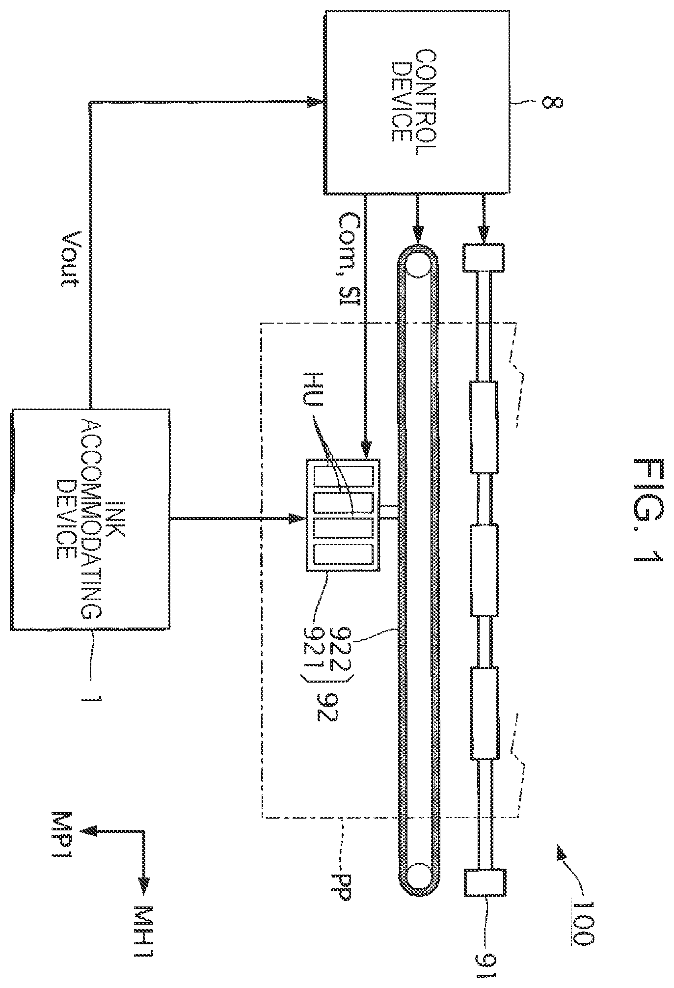
is an explanatory diagram illustrating an example of a configuration of the ink jet printer 100 according to the present embodiment.
The ink jet printer 100 is an ink jet type printing apparatus that discharges ink IK onto a medium PP. The medium PP is typically printing paper, but any print target, such as a resin film or fabric, may be used as the medium PP. In the present embodiment, conductive ink is employed as the ink IK.
In the present embodiment, the ink jet printer 100 is an example of a “liquid discharging apparatus”, and the ink IK is an example of “conductive liquid”.
As illustrated in , the ink jet printer 100 includes an ink accommodating device 1 , a control device 8 , a plurality of liquid discharging heads HU, a transport mechanism 91 , and a movement mechanism 92 .
The control device 8 includes, for example, a processing circuit such as a CPU or FPGA and a storage circuit such as a semiconductor memory, and controls each element of the ink jet printer 100 . Here, the CPU is an abbreviation of Central Processing Unit, and the FPGA is an abbreviation of Field Programmable Gate Array.
The transport mechanism 91 transports the medium PP in a sub-scanning direction MP 1 based on the control by the control device 8 .
The movement mechanism 92 reciprocates the plurality of liquid discharging heads HU in a main scanning direction MH 1 intersecting the sub-scanning direction MP 1 and in a main scanning direction MH 2 opposite to the main scanning direction MH 1 based on the control by the control device 8 . The movement mechanism 92 includes a housing case 921 that accommodates the plurality of liquid discharging heads HU, and an endless belt 922 to which the housing case 921 is fixed. The ink accommodating device 1 may be housed in the housing case 921 together with the liquid discharging head HU.
The control device 8 supplies, with respect to the liquid discharging head HU, a drive signal Com for driving the liquid discharging head HU and a control signal SI for controlling the liquid discharging head HU.
The liquid discharging head HU is driven by the drive signal Com based on the control of the control signal SI to discharge the ink IK from some or all of a plurality of nozzles provided in the liquid discharging head HU. That is, the liquid discharging head HU causes the ink IK to be discharged from some or all of the plurality of nozzles in conjunction with the transportation of the medium PP by the transport mechanism 91 and the reciprocation of the liquid discharging head HU by the movement mechanism 92 , and causes the discharged ink to land on a surface of the medium PP, thereby forming a desired image on the surface of the medium PP.
The ink accommodating device 1 accommodates the ink IK. Further, the ink accommodating device 1 supplies the ink IK accommodated in the ink accommodating device 1 to the liquid discharging head HU based on the control by the control device 8 .
In the present embodiment, the ink accommodating device 1 is an example of a “liquid accommodating device”.
In the present embodiment, it is assumed that the ink accommodating device 1 accommodates M types of the ink IK. Here, a value M is a natural number that satisfies 1≤M. More specifically, in the present embodiment, as an example, it is assumed that the ink accommodating device 1 accommodates four types of the ink IK corresponding to cyan, magenta, yellow, and black. That is, in the present embodiment, as an example, “M=4” is assumed.
In the present embodiment, it is assumed that the ink jet printer 100 includes M liquid discharging heads HU corresponding to M types of the ink IK. Specifically, in the present embodiment, as an example, it is assumed that the ink jet printer 100 includes four liquid discharging heads HU corresponding to four types of the ink IK.
In the following, among the M liquid discharging heads HU, the m-th liquid discharging head HU may be referred to as a liquid discharging head HU[m]. Here, the variable m is a natural number that satisfies 1≤m≤M.
The ink accommodating device 1 includes an ink amount detection circuit 2 that detects a remaining amount of each type of ink IK accommodated in the ink accommodating device 1 and that outputs a detection signal Vout indicating a result of the detection. The ink amount detection circuit 2 will be described later in .
1.2. Ink Accommodating Device
In the following, an overview of the ink accommodating device 1 will be described with reference to to 8 .
is a perspective view for explaining an example of a configuration of the ink accommodating device 1 .
As illustrated in , the ink accommodating device 1 includes M ink tanks TK[ 1 ] to TK[M] that correspond one-to-one to M types of ink IK accommodated in the ink accommodating device 1 , and a housing case 11 that houses the M ink tanks TK[ 1 ] to TK[M]. Specifically, in the present embodiment, the ink accommodating device 1 includes four ink tanks TK[ 1 ] to TK[ 4 ] that correspond one-to-one to four types of the ink IK of cyan, magenta, yellow, and black.
The ink tank TK[m] accommodates a type of the ink IK corresponding to the ink tank TK[m] and supplies the ink IK to the liquid discharging head HU[m]. Further, the ink tank TK[m] is provided with a supply port 12 for supplying the ink IK to an internal space of the ink tank TK[m]. Further, an electrode rod DA 1 , which is a rod-shaped electrode, and an electrode rod DA 2 , which is a rod-shaped electrode, are accommodated in the ink tank TK[m].
In the present embodiment, the ink tank TK[m] is an example of an “accommodating container”.
In the following, when the ink IK is supplied from the ink tank TK[m] to the liquid discharging head HU[m] and the ink IK accommodated inside the ink tank TK[m] decreases, a direction in which the ink IK decreases in the ink tank TK[m] is referred to as a Z 1 direction. Further, in the present embodiment, as an example, it is assumed that the electrode rod DA 1 is provided to extend in the Z 1 direction and the electrode rod DA 2 is provided to extend in the Z 1 direction. Further, in the present embodiment, it is assumed that the electrode rod DA 1 is disposed in an X 1 direction orthogonal to the Z 1 direction when viewed from the electrode rod DA 2 .
In the following, the Z 1 direction and a Z 2 direction opposite to the Z 1 direction are collectively referred to as a Z axis direction. Further, in the following, the X 1 direction along an X axis orthogonal to the Z axis direction and an X 2 direction opposite to the X 1 direction are collectively referred to as an X axis direction. Further, in the following, a Y 1 direction along a Y axis orthogonal to the Z axis direction and the X axis direction, and a Y 2 direction opposite to the Y 1 direction are collectively referred to as a Y axis direction. In the present embodiment, it is assumed that the X axis, the Y axis, and the Z axis are orthogonal to each other. However, the present disclosure is not limited to such an embodiment. The X axis, the Y axis, and the Z axis may intersect each other.
is a circuit diagram illustrating an example of a configuration of the ink amount detection circuit 2 . In the present embodiment, it is assumed that the ink accommodating device 1 is provided with M ink amount detection circuits 2 that correspond one-to-one to the M ink tanks TK[ 1 ] to TK[M]. In the present embodiment, the ink amount detection circuit 2 is an example of a “detection portion”.
As illustrated in , the ink amount detection circuit 2 includes an input terminal TnN, a node NK, a resistor RK provided between the input terminal TnN and the node NK, a detection terminal TnK electrically coupled to the node NK, an output terminal TnS electrically coupled to the node NK, and a reference potential coupling terminal TnG electrically coupled to a wiring that is set to a ground potential. The detection terminal TnK is electrically coupled to the electrode rod DA 1 via a wiring LK. The reference potential coupling terminal TnG is electrically coupled to the electrode rod DA 2 via a wiring LG.
In the present embodiment, when the ink IK is accommodated in the ink tank TK[m] and the electrode rod DA 1 and the electrode rod DA 2 are in contact with the ink IK accommodated in the ink tank TK[m], the electrode rod DA 1 and the electrode rod DA 2 are electrically coupled via the ink IK accommodated in an ink tank TK[m]. That is, when the electrode rod DA 1 and the electrode rod DA 2 are in contact with the ink IK accommodated in the ink tank TK[m], the detection terminal TnK and the reference potential coupling terminal TnG are electrically coupled via the ink IK accommodated in the ink tank TK[m]. In the present embodiment, when the electrode rod DA 1 and the electrode rod DA 2 are electrically coupled via ink IK accommodated in the ink tank TK[m], a resistor included in the ink IK that electrically couples the electrode rod DA 1 and electrode rod DA 2 is referred to as an ink resistor RT.
In the present embodiment, an input signal Vin set to a constant input potential V 0 is input to the input terminal TnN. Therefore, when the electrode rod DA 1 and the electrode rod DA 2 are electrically coupled via the ink IK accommodated in the ink tank TK[m], a potential of the node NK is determined based on the input potential V 0 of the input signal Vin, a resistance value of the resistor RK, and a resistance value of the ink resistor RT. In the present embodiment, since the input potential V 0 of the input signal Vin and the resistance value of the resistor RK are constant values, the potential of the node NK is determined based on the resistance value of the ink resistor RT. Further, the detection signal Vout indicating the potential of the node NK is output from the output terminal TnS.
is a configuration diagram illustrating an example of a configuration of the electrode rod DA 1 and the electrode rod DA 2 .
As illustrated in , the electrode rod DA 1 includes a conductive electrode configuration part ZA 11 , a conductive electrode configuration part ZA 12 , and a conductive coupling part ZA 1 t.
The electrode configuration part ZA 11 is a columnar-shaped electrode extending in the Z 1 direction and having a substantially uniform thickness, and has an outer periphery GA 11 with a length NA 11 when cutting on a plane with the Z 1 direction as a normal direction.
The electrode configuration part ZA 12 is a columnar-shaped electrode extending in the Z 1 direction and having a substantially uniform thickness, and has an outer periphery GA 12 with a length NA 12 when cutting on a plane with the Z 1 direction as the normal direction. Here, the length NA 12 is shorter than the length NA 11 . Further, the electrode configuration part ZA 12 is positioned in the Z 1 direction when viewed from the electrode configuration part ZA 11 and is coupled to the electrode configuration part ZA 11 .
The coupling part ZA 1 t is positioned in the Z 2 direction when viewed from the electrode configuration part ZA 11 , is coupled to the electrode configuration part ZA 11 , and is electrically coupled to the wiring LK. That is, the coupling part ZA 1 t electrically couples the electrode configuration part ZA 11 and the wiring LK.
In the present specification, “substantially uniform” is a concept that includes a case of being completely uniform and a case where it can be regarded as uniform when an error is considered. Specifically, in the present specification, “substantially uniform” is a concept that includes a case where it can be regarded as uniform when an error of substantially 10% is considered. Similarly, in the present specification, “substantially the same” is a concept that includes a case of being completely the same and a case where it can be regarded as the same when an error is considered. Specifically, in the present specification, “substantially the same” is a concept that includes a case where it can be regarded as the same when an error of substantially 10% is considered. In the present specification, expression similar to “substantially uniform” or “substantially the same” is the same as “substantially uniform” and “substantially the same”.
The electrode rod DA 2 is a columnar-shaped electrode extending in the Z 1 direction and includes a conductive electrode configuration part ZA 2 and a conductive coupling part ZA 2 t.
The electrode configuration part ZA 2 is a columnar-shaped electrode extending in the Z 1 direction and having a substantially uniform thickness, and has an outer periphery GA 2 with a length NA 2 when cutting on a plane with the Z 1 direction as the normal direction.
The coupling part ZA 2 t is positioned in the Z 2 direction when viewed from the electrode configuration part ZA 2 , is coupled to the electrode configuration part ZA 2 , and is electrically coupled to the wiring LG. That is, the coupling part ZA 2 t electrically couples the electrode configuration part ZA 2 and the wiring LG.
As described above, in the present embodiment, it is assumed that the electrode configuration part ZA 11 is positioned in the X 1 direction when viewed from the electrode configuration part ZA 2 . In the following, a distance between the electrode configuration part ZA 11 and the electrode configuration part ZA 2 in the X 1 direction is referred to as a distance XA 1 . Further, as described above, in the present embodiment, it is assumed that the electrode configuration part ZA 12 is positioned in the X 1 direction when viewed from the electrode configuration part ZA 2 . In the following, a distance between the electrode configuration part ZA 12 and the electrode configuration part ZA 2 in the X 1 direction is referred to as a distance XA 2 . In the present embodiment, the distance XA 2 is longer than the distance XA 1 .
are explanatory diagrams for explaining an example of the ink resistor RT formed between the electrode rod DA 1 and the electrode rod DA 2 .
In the following, a distance from a bottom surface TKB of the ink tank TK[m] to a liquid level SF of the ink IK accommodated in the ink tank TK[m] in the Z axis direction is referred to as an ink liquid level distance SZ.
As illustrated in , in the present embodiment, it is assumed that the electrode rod DA 1 and the electrode rod DA 2 are provided such that a distance, which is from an end portion of the electrode rod DA 1 in the Z 1 direction to the bottom surface TKB of the ink tank TK[m], in the Z axis direction and a distance, which is from an end portion of the electrode rod DA 2 in the Z 1 direction to the bottom surface TKB of the ink tank TK[m], in the Z axis direction become a distance HE. That is, in the present embodiment, it is assumed that the electrode rod DA 1 and the electrode rod DA 2 are provided such that a distance, which is from an end portion of the electrode configuration part ZA 12 in the Z 1 direction to the bottom surface TKB of the ink tank TK[m], in the Z axis direction and a distance, which is from an end portion of the electrode configuration part ZA 2 in the Z 1 direction to the bottom surface TKB of the ink tank TK[m], in the Z axis direction are substantially the same distance.
Further, in the present embodiment, it is assumed that the electrode rod DA 1 is provided such that a distance, which is from an end portion of the electrode configuration part ZA 11 in the Z 1 direction to the bottom surface TKB of the ink tank TK[m], in the Z axis direction becomes a distance H 2 . Here, the distance H 2 is a distance longer than the distance HE.
Further, in the present embodiment, it is assumed that the electrode rod DA 1 and the electrode rod DA 2 are provided such that a distance, which is from an end portion of the electrode configuration part ZA 11 in the Z 2 direction to the bottom surface TKB of the ink tank TK[m], in the Z axis direction and a distance, which is from an end portion of the electrode configuration part ZA 2 in the Z 2 direction to the bottom surface TKB of the ink tank TK[m], in the Z axis direction become a distance H 1 . Here, the distance H 1 is a distance longer than the distance H 2 .
As illustrated in , when the ink IK is present between the electrode configuration part ZA 11 and the electrode configuration part ZA 2 , that is, when the ink liquid level distance SZ is equal to or longer than the distance H 2 , the electrode configuration part ZA 11 and the electrode configuration part ZA 2 are electrically coupled through the ink IK. In the following, a resistor included in the ink IK that electrically couples the electrode configuration part ZA 11 and the electrode configuration part ZA 2 is referred to as a resistor RRA 1 .
As illustrated in , when the ink IK is present between the electrode configuration part ZA 12 and the electrode configuration part ZA 2 , that is, when the ink liquid level distance SZ is equal to or longer than the distance HE, the electrode configuration part ZA 12 and the electrode configuration part ZA 2 are electrically coupled through the ink IK. In the following, a resistor included in the ink IK that electrically couples the electrode configuration part ZA 12 and the electrode configuration part ZA 2 is referred to as a resistor RRA 2 .
When the ink liquid level distance SZ is equal to or longer than the distance HE and shorter than the distance H 2 , the resistor RRA 2 becomes the above-described ink resistor RT.
Further, when the ink liquid level distance SZ is equal to or longer than the distance H 2 , a composite resistance of the resistor RRA 1 and the resistor RRA 2 when the resistor RRA 1 and the resistor RRA 2 are coupled in parallel is the ink resistor RT described above.
is an explanatory diagram for explaining an example of a relationship between the ink liquid level distance SZ and the ink resistor RT. Specifically, illustrates an example of a resistance value change curve CRA indicating a relationship between the ink liquid level distance SZ and the resistance value of the ink resistor RT when the horizontal axis is set to the ink liquid level distance SZ and the vertical axis is set to the resistance value of the ink resistor RT.
As described above, when the ink liquid level distance SZ is shorter than the distance HE, the electrode rod DA 1 is not in contact with the ink IK, and the electrode rod DA 2 is not in contact with the ink IK. That is, when the ink liquid level distance SZ is shorter than the distance HE, the electrode rod DA 1 and the electrode rod DA 2 are in a state of not being electrically coupled to each other. Therefore, as indicated by the resistance value change curve CRA in , when the ink liquid level distance SZ is shorter than the distance HE, the ink resistor RT has a large resistance value as compared with the case where the ink liquid level distance SZ is equal to or longer than the distance HE and the electrode rod DA 1 and the electrode rod DA 2 are electrically coupled through the ink IK.
Further, when the ink liquid level distance SZ is equal to or longer than the distance HE and shorter than the distance H 2 , the electrode configuration part ZA 12 of the electrode rod DA 1 is in contact with the ink IK, and the electrode configuration part ZA 2 of the electrode rod DA 2 is in contact with the ink IK. That is, when the ink liquid level distance SZ is equal to or longer than the distance HE and shorter than the distance H 2 , the ink resistor RT of the ink IK that electrically couples the electrode rod DA 1 and the electrode rod DA 2 becomes the resistor RRA 2 . The resistance value of the resistor RRA 2 becomes smaller as a cross-sectional area becomes larger. Therefore, as indicated by the resistance value change curve CRA, when the ink liquid level distance SZ is equal to or longer than the distance HE and shorter than the distance H 2 , the ink resistor RT becomes smaller as the ink liquid level distance SZ becomes longer.
Further, when the ink liquid level distance SZ is equal to or longer than the distance H 2 , the electrode configuration part ZA 11 and the electrode configuration part ZA 12 of the electrode rod DA 1 is in contact with the ink IK, and the electrode configuration part ZA 2 of the electrode rod DA 2 is in contact with the ink IK. That is, when the ink liquid level distance SZ is equal to or longer than the distance H 2 , the ink resistor RT of the ink IK that electrically couples the electrode rod DA 1 and the electrode rod DA 2 becomes the composite resistance of the resistor RRA 1 and the resistor RRA 2 when the resistor RRA 1 and the resistor RRA 2 are coupled in parallel.
The resistance value of the resistor RRA 1 becomes smaller as a cross-sectional area becomes larger. Therefore, as indicated by the resistance value change curve CRA, when the ink liquid level distance SZ is equal to or longer than the distance H 2 , the ink resistor RT becomes smaller as the ink liquid level distance SZ becomes longer.
Further, a resistance value of the composite resistance of the resistor RRA 1 and the resistor RRA 2 when the resistor RRA 1 and the resistor RRA 2 are coupled in parallel is smaller than the resistance value of the resistor RRA 2 . Therefore, as indicated by the resistance value change curve CRA, when the ink liquid level distance SZ is equal to or longer than the distance H 2 , the ink resistor RT becomes smaller as compared with the case where the ink liquid level distance SZ is shorter than the distance H 2 .
In the present embodiment, the length NA 11 of the outer periphery GA 11 of the electrode configuration part ZA 11 is longer than the length NA 12 of the outer periphery GA 12 of the electrode configuration part ZA 12 . In the present embodiment, the distance XA 1 between the electrode configuration part ZA 11 and the electrode configuration part ZA 2 is shorter than the distance XA 2 between the electrode configuration part ZA 12 and the electrode configuration part ZA 2 . Therefore, as in the present embodiment, when the length NA 11 is longer than the length NA 12 and the distance XA 1 is shorter than the distance XA 2 , the resistance value of the resistor RRA 1 becomes smaller, for example, as compared with the case where the length NA 11 and the length NA 12 are the same length, and the distance XA 1 and the distance XA 2 are the same length. Therefore, in the present embodiment, the resistance value change curve CRA includes a change region Ar-RA where the ink resistor RT is changed greatly at a boundary between a case where the ink liquid level distance SZ is equal to or longer than the distance H 2 and the composite resistance in which the resistor RRA 1 and the resistor RRA 2 are coupled in parallel is the ink resistor RT, and a case where the ink liquid level distance SZ is shorter than the distance H 2 and only the resistor RRA 2 is the ink resistor RT.
is an explanatory diagram for explaining an example of a relationship between the ink liquid level distance SZ and the detection signal Vout. Specifically, illustrates an example of a potential change curve CVA indicating the relationship between the ink liquid level distance SZ in the ink tank TK[m] and a potential of the detection signal Vout when the horizontal axis is set to the ink liquid level distance SZ and the vertical axis is set to the potential of the detection signal Vout.
As described above, the potential of the detection signal Vout is determined based on the ink resistor RT. Specifically, when the resistance value of the ink resistor RT is large, the potential of the detection signal Vout also becomes high as compared with a case where the resistance value is small.
Therefore, as indicated by the potential change curve CVA in , when the ink liquid level distance SZ is equal to or longer than the distance HE, the detection signal Vout has a smaller resistance value as compared with the case where the ink liquid level distance SZ is shorter than the distance HE. Further, as indicated by the potential change curve CVA, when the ink liquid level distance SZ is equal to or longer than the distance H 2 , the detection signal Vout has a smaller resistance value as compared with the case where the ink liquid level distance SZ is shorter than the distance H 2 . That is, as indicated by the potential change curve CVA, the potential of the detection signal Vout becomes lower as the ink liquid level distance SZ becomes longer.
As described above, the resistance value change curve CRA includes the change region Ar-RA where a change rate of the resistance value of the ink resistor RT becomes larger with respect to a change in the ink liquid level distance SZ. Therefore, as illustrated in , the potential change curve CVA also includes a change region Ar-VA where a change rate of the potential of the detection signal Vout becomes larger with respect to the change in the ink liquid level distance SZ.
In the following, when a temperature of the ink IK in the ink tank TK[m] is a reference temperature t 1 and when the ink liquid level distance SZ in the ink tank TK[m] is the distance HE, the potential indicated by the detection signal Vout is referred to as a threshold potential VthE. Further, in the following, when a temperature of the ink IK in the ink tank TK[m] is a reference temperature t 1 and when the ink liquid level distance SZ in the ink tank TK[m] is the distance H 2 , the potential indicated by the detection signal Vout is referred to as a threshold potential Vth 2 .
Here, the reference temperature t 1 is, for example, the temperature of the ink IK in the ink tank TK[m] when the ink jet printer 100 is used in the standard usage environment of the ink jet printer 100 . Further, the reference temperature t 1 may be, for example, an atmospheric temperature of the ink jet printer 100 when the ink jet printer 100 is used in the standard usage environment of the ink jet printer 100 . Further, the reference temperature t 1 may be, for example, a temperature of the standard usage environment of the ink IK.
In the present embodiment, the ink amount detection circuit 2 detects that a remaining amount of the ink IK in the ink tank TK[m] is less than a remaining amount of ink corresponding to the distance HE by outputting the detection signal Vout having a potential higher than the threshold potential VthE.
The remaining amount of ink corresponding to the distance HE is, for example, the minimum remaining amount of ink out of the remaining amount of ink in which the ink IK can be discharged from the liquid discharging head HU[m]. However, the remaining amount of ink corresponding to the distance HE may be, for example, a remaining amount of ink such that a difference with the minimum remaining amount of ink, of the remaining amount of ink in which the ink IK can be discharged from the liquid discharging head HU[m], is a predetermined amount. Here, the predetermined amount may be, for example, an amount less than the amount of ink necessary for the ink jet printer 100 to form an image on one sheet of medium PP and a remaining amount of ink in which the ink IK can be discharged a predetermined number of times from the liquid discharging head HU[m]. That is, the remaining amount of ink corresponding to the distance HE may be a remaining amount of ink corresponding to a so-called “ink end” state.
Further, the ink amount detection circuit 2 detects that the remaining amount of the ink IK in the ink tank TK[m] is less than a remaining amount of ink corresponding to the distance H 2 and equal to or greater than the remaining amount of ink corresponding to the distance HE by outputting the detection signal Vout having a potential higher than the threshold potential Vth 2 and equal to or lower than the threshold potential VthE.
The remaining amount of ink corresponding to the distance H 2 is, for example, a remaining amount of ink in which the ink IK can be continuously discharged from the liquid discharging head HU[m] for predetermined time or longer. Here, the predetermined time may be, for example, time required for the ink jet printer 100 to form an image on one sheet of medium PP. Further, the predetermined time may be, for example, time required for the ink jet printer 100 to form an image on a predetermined number of media PP. That is, the remaining amount of ink corresponding to the distance HE may be a remaining amount of ink corresponding to a so-called “near end” state.
In the present embodiment, the control device 8 controls a notification device (not illustrated) such that the remaining amount of ink indicated by the detection signal Vout is notified to a user of the ink jet printer 100 by, for example, audio or video based on the detection signal Vout supplied from the ink accommodating device 1 .
1.3. Ink Accommodating Device According to Reference Example
In the following, an overview of an ink accommodating device 1 W according to a reference example will be explained with reference to to 13 .
is a configuration diagram for explaining an example of a configuration of an electrode rod DW 1 and an electrode rod DW 2 provided in the ink accommodating device 1 W. It is assumed that the ink accommodating device 1 W is configured in the same manner as the ink accommodating device 1 according to the first embodiment regarding the ink tank TK[m] except that the electrode rod DW 1 is accommodated instead of the electrode rod DA 1 , and the electrode rod DW 2 is accommodated instead of the electrode rod DA 2 .
As illustrated in , the electrode rod DW 1 is a columnar-shaped electrode extending in the Z 1 direction and includes a conductive electrode configuration part ZW 1 and a conductive coupling part ZW 1 t.
The electrode configuration part ZW 1 is a columnar-shaped electrode extending in the Z 1 direction and having a substantially uniform thickness, and has an outer periphery GW 1 with a length NW 1 when cutting on a plane with the Z 1 direction as the normal direction. In the reference example, it is assumed that a length NW 1 is substantially the same length as the length NA 12 of the outer periphery GA 12 of the electrode configuration part ZA 12 according to the first embodiment.
The coupling part ZW 1 t is positioned in the Z 2 direction when viewed from the electrode configuration part ZW 1 , is coupled to the electrode configuration part ZW 1 , and is electrically coupled to the wiring LK. That is, the coupling part ZW 1 t electrically couples the electrode configuration part ZW 1 and the wiring LK.
The electrode rod DW 2 is a columnar-shaped electrode extending in the Z 1 direction and includes a conductive electrode configuration part ZW 2 and a conductive coupling part ZW 2 t.
The electrode configuration part ZW 2 is a columnar-shaped electrode extending in the Z 1 direction and having a substantially uniform thickness, and has an outer periphery GW 2 with a length NW 2 when cutting on a plane with the Z 1 direction as the normal direction. In the reference example, it is assumed that a length NW 2 is substantially the same length as the length NA 2 of the outer periphery GA 2 of the electrode configuration part ZA 2 according to the first embodiment.
The coupling part ZW 2 t is positioned in the Z 2 direction when viewed from the electrode configuration part ZW 2 , is coupled to the electrode configuration part ZW 2 , and is electrically coupled to the wiring LG. That is, the coupling part ZW 2 t electrically couples the electrode configuration part ZW 2 and the wiring LG.
In the reference example, it is assumed that the electrode configuration part ZW 1 is positioned in the X 1 direction when viewed from the electrode configuration part ZW 2 . In the following, a distance between the electrode configuration part ZW 1 and the electrode configuration part ZW 2 in the X 1 direction is referred to as a distance XW. In the reference example, it is assumed that the distance XW is substantially the same length as the distance XA 2 between the electrode configuration part ZA 12 and the electrode configuration part ZA 2 according to the first embodiment.
Further, in the reference example, it is assumed that the electrode rod DW 1 and the electrode rod DW 2 are provided such that a distance, which is from an end portion of the electrode configuration part ZW 1 in the Z 1 direction to the bottom surface TKB of the ink tank TK[m], and a distance, which is from an end portion of the electrode configuration part ZW 2 in the Z 1 direction to the bottom surface TKB of the ink tank TK[m], become a distance HE.
Further, in the reference example, it is assumed that the electrode rod DW 1 and the electrode rod DW 2 are provided such that a distance, which is from an end portion of the electrode configuration part ZW 1 in the Z 2 direction to the bottom surface TKB of the ink tank TK[m], and a distance, which is from an end portion of the electrode configuration part ZW 2 in the Z 2 direction to the bottom surface TKB of the ink tank TK[m], become a distance H 1 .
is an explanatory diagram for explaining an example of a relationship between the ink liquid level distance SZ and an ink resistor RT according to the reference example. Specifically, illustrates an example of a resistance value change curve CRW indicating a relationship between the ink liquid level distance SZ and a resistance value of the ink resistor RT according to the reference example when the horizontal axis is set to the ink liquid level distance SZ and the vertical axis is set to the resistance value of the ink resistor RT according to the reference example. Here, the ink resistor RT according to the reference example is a resistor included in the ink IK that electrically couples the electrode rod DW 1 and the electrode rod DW 2 when the electrode rod DW 1 and the electrode rod DW 2 , which are accommodated in the ink tank TK[m], are electrically coupled via the ink IK accommodated in the ink tank TK[m]. In the following, in order to distinguish the ink resistor RT according to the first embodiment, the ink resistor RT according to the reference example may be referred to as an ink resistor RTW.
For convenience of description, illustrates the resistance value change curve CRA with a broken line together with the resistance value change curve CRW.
As described above, in the reference example, when the ink liquid level distance SZ is shorter than the distance HE, the electrode rod DW 1 is not in contact with the ink IK, and the electrode rod DW 2 is not in contact with the ink IK. Therefore, as indicated by the resistance value change curve CRW in , when the ink liquid level distance SZ is shorter than the distance HE, the ink resistor RTW has a large resistance value as compared with the case where the electrode rod DW 1 and the electrode rod DW 2 are electrically coupled through the ink IK.
Further, when the ink liquid level distance SZ is equal to or longer than the distance HE, the electrode rod DW 1 is in contact with the ink IK and the electrode rod DW 2 is in contact with the ink IK. Therefore, as indicated by the resistance value change curve CRW, when the ink liquid level distance SZ is equal to or longer than the distance HE, the ink resistor RTW becomes smaller as the ink liquid level distance SZ becomes longer.
As described above, in the reference example, it is assumed that the electrode configuration part ZW 1 has an outer periphery with substantially the same length as that of the electrode configuration part ZA 12 , the electrode configuration part ZW 2 has an outer periphery with substantially the same length as that of the electrode configuration part ZA 2 , and the distance XW is substantially the same length as the distance XA 2 . Therefore, when the ink liquid level distance SZ is shorter than the distance H 2 , the resistance value change curve CRW has substantially the same shape as that of the resistance value change curve CRA according to the first embodiment.
Further, as described above, in the reference example, it is assumed that the electrode configuration part ZW 1 and the electrode configuration part ZW 2 are columnar-shaped electrodes having a substantially uniform thickness. That is, in the reference example, it is assumed that the electrode configuration part ZW 1 has the outer periphery with a length shorter than that of the electrode configuration part ZA 11 , the electrode configuration part ZW 2 has an outer periphery with substantially the same length as that of the electrode configuration part ZA 2 , and the distance XW is longer than the distance XA 1 . Therefore, when the ink liquid level distance SZ is equal to or longer than the distance H 2 , the resistance value change curve CRW indicates a potential higher than the potential indicated by the resistance value change curve CRA according to the first embodiment.
Further, the resistance value change curve CRW does not include a change region Ar-RA where the ink resistor RT is changed suddenly like the resistance value change curve CRA according to the first embodiment but includes a smooth shape in which the ink resistor RTW is continuously decreased as the ink liquid level distance SZ becomes longer.
is an explanatory diagram for explaining an example of a relationship between the ink liquid level distance SZ and the detection signal Vout according to the reference example. Specifically, illustrates an example of a potential change curve CVW indicating a relationship between the ink liquid level distance SZ and the potential of the detection signal Vout according to the reference example when the horizontal axis is set to the ink liquid level distance SZ and the vertical axis is set to the potential of the detection signal Vout according to the reference example. Here, the detection signal Vout according to the reference example is a detection signal Vout output by the ink accommodating device 1 W. In the following, in order to distinguish the detection signal Vout according to the first embodiment, the detection signal Vout according to the reference example may be referred to as a detection signal Vout-W.
For convenience of description, illustrates the potential change curve CVA with a broken line together with the potential change curve CVW.
As indicated by the potential change curve CVW in , the potential of the detection signal Vout-W becomes lower as the ink liquid level distance SZ becomes longer.
Further, as described above, the resistance value change curve CRW does not have a step as in the change region Ar-RA. Therefore, the potential change curve CVW does not include a change region Ar-VA where the detection signal Vout is changed suddenly like the potential change curve CVA according to the first embodiment but includes a smooth shape in which the detection signal Vout-W is continuously decreased as the ink liquid level distance SZ becomes longer.
is an explanatory diagram for explaining a temperature change of the resistance value change curve CRW in accordance with a temperature change of the ink IK in the ink tank TK[m] according to the reference example.
Specifically, in , the resistance value change curve CRW when the temperature of the ink IK in the ink tank TK[m] is the reference temperature t 1 is represented as a resistance value change curve CRW (t 1 ), and the resistance value change curve CRW when the temperature of the ink IK in the ink tank TK[m] is a temperature t 2 different from the reference temperature t 1 is represented as a resistance value change curve CRW (t 2 ). In , it is assumed that the resistance value change curve CRW (t 1 ) is the same curve as the resistance value change curve CRW in .
As illustrated in , when the temperature of the ink IK in the ink tank TK[m] is changed, the resistance value indicated by the resistance value change curve CRW is also changed. Specifically, when the temperature of the ink IK in the ink tank TK[m] is changed from the reference temperature t 1 to the temperature t 2 , the resistance value of the ink resistor RTW indicated by the resistance value change curve CRW is also changed. That is, when the ink liquid level distance SZ is the same value, the resistance value of the ink resistor RTW indicated by the resistance value change curve CRW (t 1 ) and the resistance value of the ink resistor RTW indicated by the resistance value change curve CRW (t 2 ) are different from each other.
Although illustrates a case where the resistance value of the ink resistor RTW indicated by the resistance value change curve CRW is changed to a small value in accordance with the temperature change of the ink IK in the ink tank TK[m], the present disclosure is not limited to such embodiments. The resistance value of the ink resistor RTW indicated by the resistance value change curve CRW may be changed to a large value in accordance with the temperature change of the ink IK in the ink tank TK[m].
is an explanatory diagram for explaining a temperature change of the potential change curve CVW in accordance with the temperature change of the ink IK in the ink tank TK[m] according to the reference example.
Specifically, in , the potential change curve CVW when the temperature of the ink IK in the ink tank TK[m] is the reference temperature t 1 is represented as a potential change curve CVW (t 1 ), and the potential change curve CVW when the temperature of the ink IK in the ink tank TK[m] is the temperature t 2 is represented as a potential change curve CVW (t 2 ). In , it is assumed that the potential change curve CVW (t 1 ) is the same curve as the potential change curve CVW in .
As illustrated in , when the temperature of the ink IK in the ink tank TK[m] is changed, the potential indicated by the potential change curve CVW is also changed. Specifically, when the temperature of the ink IK in the ink tank TK[m] is changed from the reference temperature t 1 to the temperature t 2 , the potential of the detection signal Vout-W indicated by the potential change curve CVW is also changed. That is, when the ink liquid level distance SZ is the same value, the potential of the detection signal Vout-W indicated by the potential change curve CVW (t 1 ) and the potential of the detection signal Vout-W indicated by the potential change curve CVW (t 2 ) are different from each other.
Although illustrates a case where the potential of the detection signal Vout-W indicated by the potential change curve CVW is changed to a small value in accordance with the temperature change of the ink IK in the ink tank TK[m], the present disclosure is not limited to such embodiments. The potential of the detection signal Vout-W indicated by the potential change curve CVW may be changed to a large value in accordance with the temperature change of the ink IK in the ink tank TK[m].
As described above, in the ink accommodating device 1 W according to the reference example, even when there is no change in the remaining amount of the ink IK in the ink tank TK[m], the potential of the detection signal Vout-W output from the ink accommodating device 1 W is changed in accordance with the temperature change of the ink IK in the ink tank TK[m]. Therefore, the ink accommodating device 1 W according to the reference example may not be able to appropriately detect the remaining amount of the ink IK.
Specifically, in the example illustrated in , when the temperature of the ink IK in the ink tank TK[m] is the reference temperature t 1 , the ink accommodating device 1 W detects that the remaining amount of the ink IK in the ink tank TK[m] is less than the remaining amount of ink corresponding to the distance HE by the fact that the potential of the detection signal Vout-W is a potential higher than the threshold potential VthE, and detects that the remaining amount of the ink IK in the ink tank TK[m] is less than the remaining amount of ink corresponding to the distance H 2 by the fact that the potential of the detection signal Vout-W is a potential higher than the threshold potential Vth 2 . In other words, when the temperature of the ink IK in the ink tank TK[m] is the reference temperature t 1 , the ink accommodating device 1 W detects that the remaining amount of the ink IK in the ink tank TK[m] is equal to or greater than the remaining amount of ink corresponding to the distance HE by the fact that the potential of the detection signal Vout-W is equal to or lower than the threshold potential VthE, and detects that the remaining amount of the ink IK in the ink tank TK[m] is equal to or greater than the remaining amount of ink corresponding to the distance H 2 by the fact that the potential of the detection signal Vout-W is equal to or lower than the threshold potential Vth 2 .
However, in the example illustrated in , when the temperature of the ink IK in the ink tank TK[m] is the temperature t 2 , even when the potential of the detection signal Vout-W is equal to or lower than the threshold potential VthE, there is a possibility that the remaining amount of the ink IK in the ink tank TK[m] is less than the remaining amount of ink corresponding to the distance HE, and even when the potential of the detection signal Vout-W is equal to or lower than the threshold potential Vth 2 , there is a possibility that the remaining amount of the ink IK in the ink tank TK[m] is less than the remaining amount of ink corresponding to the distance H 2 .
Further, in the example illustrated in , when the temperature of the ink IK in the ink tank TK[m] is the temperature t 2 , even when the potential of the detection signal Vout-W is equal to or lower than the threshold potential Vth 2 , there is a possibility that the remaining amount of the ink IK in the ink tank TK[m] is less than the remaining amount of ink corresponding to the distance HE. That is, when the potential of the detection signal Vout-W is equal to or lower than the threshold potential Vth 2 and when the remaining amount of the ink IK in the ink tank TK[m] is equal to or greater than the remaining amount of ink corresponding to the distance H 2 , although the user of the ink jet printer 100 is aware of this, in reality, there is a possibility that the remaining amount of the ink IK in the ink tank TK[m] is equal to or less than the remaining amount of ink corresponding to the distance HE.
That is, in the example illustrated in , when the temperature of the ink IK in the ink tank TK[m] is the temperature t 2 , it becomes difficult for the ink accommodating device 1 W to understand the remaining amount of the ink IK in the ink tank TK[m] based on the potential of the detection signal Vout-W. That is, in the ink accommodating device 1 W, there is a possibility that it is difficult to detect the remaining amount of the ink IK in the ink tank TK[m] based on the detection signal Vout-W.
In the ink accommodating device 1 W, an embodiment can be considered in which the remaining amount of the ink IK in the ink tank TK[m] is detected based on the potential indicated by the corrected detection signal Vout-W by adding a temperature detection device that detects the temperature of the ink IK in the ink tank TK[m] and correcting the potential indicated by the detection signal Vout-W according to a detection result of the temperature detection device. However, in this case, there is a concern that the configuration of the ink accommodating device 1 W is complicated as compared with the above-described first embodiment.
1.4. Effects of First Embodiment
Next, the effect of the present embodiment will be explained with reference to to 15 .
is an explanatory diagram for explaining a temperature change of the resistance value change curve CRA in accordance with the temperature change of the ink IK in the ink tank TK[m] according to the first embodiment.
Specifically, in , the resistance value change curve CRA when the temperature of the ink IK in the ink tank TK[m] is the reference temperature t 1 is represented as a resistance value change curve CRA (t 1 ), and the resistance value change curve CRA when the temperature of the ink IK in the ink tank TK[m] is the temperature t 2 is represented as a resistance value change curve CRA (t 2 ). In , it is assumed that the resistance value change curve CRA (t 1 ) is the same curve as the resistance value change curve CRA in .
As illustrated in , when the temperature of the ink IK in the ink tank TK[m] is changed, the resistance value indicated by the resistance value change curve CRA is also changed. Specifically, when the temperature of the ink IK in the ink tank TK[m] is changed from the reference temperature t 1 to the temperature t 2 , the resistance value of the ink resistor RT indicated by the resistance value change curve CRA is also changed. That is, when the ink liquid level distance SZ is the same value, the resistance value of the ink resistor RT indicated by the resistance value change curve CRA (t 1 ) and the resistance value of the ink resistor RT indicated by the resistance value change curve CRA (t 2 ) are different from each other.
Although illustrates a case where the resistance value of the ink resistor RT indicated by the resistance value change curve CRA is changed to a small value in accordance with the temperature change of the ink IK in the ink tank TK[m], the present disclosure is not limited to such embodiments. The resistance value of the ink resistor RT indicated by the resistance value change curve CRA may be changed to a large value in accordance with the temperature change of the ink IK in the ink tank TK[m].
is an explanatory diagram for explaining a temperature change of the potential change curve CVA in accordance with the temperature change of the ink IK in the ink tank TK[m] according to the first embodiment.
Specifically, in , the potential change curve CVA when the temperature of the ink IK in the ink tank TK[m] is the reference temperature t 1 is represented as a potential change curve CVA (t 1 ), and the potential change curve CVA when the temperature of the ink IK in the ink tank TK[m] is the temperature t 2 is represented as a potential change curve CVA (t 2 ). In , it is assumed that the potential change curve CVA (t 1 ) is the same curve as the potential change curve CVA in .
As illustrated in , when the temperature of the ink IK in the ink tank TK[m] is changed, the potential indicated by the potential change curve CVA is also changed. Specifically, when the temperature of the ink IK in the ink tank TK[m] is changed from the reference temperature t 1 to the temperature t 2 , the potential of the detection signal Vout indicated by the potential change curve CVA is also changed. That is, when the ink liquid level distance SZ is the same value, the potential of the detection signal Vout indicated by the potential change curve CVA (t 1 ) and the potential of the detection signal Vout indicated by the potential change curve CVA (t 2 ) are different from each other.
Although illustrates a case where the potential of the detection signal Vout indicated by the potential change curve CVA is changed to a small value in accordance with the temperature change of the ink IK in the ink tank TK[m], the present disclosure is not limited to such embodiments. The potential of the detection signal Vout indicated by the potential change curve CVA may be changed to a large value in accordance with the temperature change of the ink IK in the ink tank TK[m].
As described above, the resistance value change curve CRA according to the first embodiment includes the change region Ar-RA in a part where the ink liquid level distance SZ becomes the distance H 2 . That is, in the change region Ar-RA including the part where the ink liquid level distance SZ becomes the distance H 2 in the resistance value change curve CRA, the resistance value of the ink resistor RT indicated by the resistance value change curve CRA is changed greatly. Therefore, a part of the change region Ar-RA included in the resistance value change curve CRA (t 1 ) and a part of the change region Ar-RA included in the resistance value change curve CRA (t 2 ) overlap each other in the vertical axis direction of the graph illustrated in .
As described above, the potential change curve CVA according to the first embodiment also includes the change region Ar-VA, which is a region where the potential of the detection signal Vout indicated by the potential change curve CVA is changed greatly in the part where the ink liquid level distance SZ becomes the distance H 2 . In the vertical axis direction of the graph illustrated in , the change region Ar-VA, which is included in the potential change curve CVA (t 1 ), includes a part where the detection signal Vout becomes the threshold potential Vth 2 . That is, the change region Ar-VA included in the potential change curve CVA (t 1 ) intersects a straight line “Vout=Vth 2 ” in the graph illustrated in .
Further, since the change region Ar-VA is a region where the potential of the detection signal Vout indicated by the potential change curve CVA is changed greatly, a part of the change region Ar-VA included in the potential change curve CVA (t 1 ) and a part of the change region Ar-VA included in the potential change curve CVA (t 2 ) overlap each other in the vertical axis direction of the graph shown in . Therefore, when a temperature difference between the reference temperature t 1 and the temperature t 2 is within a predetermined temperature difference, the change region Ar-VA, which is included in the potential change curve CVA (t 2 ), also includes a part where the detection signal Vout becomes the threshold potential Vth 2 . That is, when the temperature difference between the reference temperature t 1 and the temperature t 2 is within the predetermined temperature difference, the change region Ar-VA included in the potential change curve CVA (t 2 ) intersects the straight line “Vout=Vth 2 ” in the graph illustrated in .
Here, the predetermined temperature difference may be, for example, a temperature difference between the temperature of the ink IK in the ink tank TK[m] and the reference temperature t 1 when the ink jet printer 100 is used in the limited usage environment of the ink jet printer 100 . Further, the predetermined temperature difference may be, for example, a temperature difference between the atmospheric temperature of the ink jet printer 100 and the reference temperature t 1 when the ink jet printer 100 is used in the limited usage environment of the ink jet printer 100 . Further, the predetermined temperature difference may be, for example, a temperature difference between the temperature of the limited usage environment of the ink IK and the reference temperature t 1 .
Therefore, according to the first embodiment, compared to the reference example, in addition to the case where the temperature of the ink IK in the ink tank TK[m] is the reference temperature t 1 , even when the temperature of the ink IK in the ink tank TK[m] is the temperature t 2 , there is high possibility that a detection is made that the remaining amount of the ink IK in the ink tank TK[m] is less than the remaining amount of ink corresponding to the distance HE by the fact that the potential of the detection signal Vout is a potential higher than the threshold potential VthE, and a detection is made that the remaining amount of the ink IK in the ink tank TK[m] is less than the remaining amount of ink corresponding to the distance H 2 by the fact that the potential of the detection signal Vout is a potential higher than the threshold potential Vth 2 . According to the first embodiment, compared to the reference example, even when the potential of the detection signal Vout is equal to or lower than the threshold potential VthE, the possibility of erroneous detection can be reduced in which the remaining amount of the ink IK in the ink tank TK[m] is less than the remaining amount of ink corresponding to the distance HE, and even when the potential of the detection signal Vout is equal to or lower than the threshold potential Vth 2 , the possibility of erroneous detection can be reduced in which the remaining amount of ink IK in the ink tank TK[m] is less than the remaining amount of ink corresponding to the distance H 2 .
That is, according to the ink accommodating device 1 of the first embodiment, compared to the ink accommodating device 1 W according to the reference example, the remaining amount of the ink IK in the ink tank TK[m] can be accurately detected based on the detection signal Vout.
In the present embodiment, although a description is made by exemplifying the case where change occurs in the resistance value of the ink resistor RT due to the temperature change of the ink IK in the ink tank TK[m], and as a result, change occurs in the potential of the detection signal Vout indicated by the potential change curve CVA, the present disclosure is not limited to such an embodiment. The present embodiment can be applied to any case where fluctuation occurs in the potential of the detection signal Vout indicated by the potential change curve CVA.
For example, according to the present embodiment, even when change occurs in the potential of the detection signal Vout indicated by the potential change curve CVA due to deterioration or modification of the ink IK in the ink tank TK[m], compared to the reference example, the remaining amount of the ink IK in the ink tank TK[m] can be accurately detected based on the detection signal Vout. Further, according to the present embodiment, even when change occurs in the potential of the detection signal Vout indicated by the potential change curve CVA due to noise being superimposed on the detection signal Vout, compared to the reference example, the remaining amount of the ink IK in the ink tank TK[m] can be accurately detected based on the detection signal Vout.
1.5. Conclusion of First Embodiment
As described above, the ink jet printer 100 according to the present embodiment includes: the ink tank TK[m] accommodating the conductive ink IK; the rod-shaped electrode rod DA 1 accommodated in the ink tank TK[m]; the rod-shaped electrode rod DA 2 accommodated in the ink tank TK[m]; the ink amount detection circuit 2 that is electrically coupled to the electrode rod DA 1 and the electrode rod DA 2 and that detects the remaining amount of the ink IK accommodated in the ink tank TK[m] in response to the electric signal from at least one of the electrode rod DA 1 and the electrode rod DA 2 ; and the liquid discharging head HU[m] discharging the ink IK supplied from the ink tank TK[m], in which the electrode rod DA 1 includes the electrode configuration part ZA 11 having the outer periphery GA 11 with the length NA 11 and the electrode configuration part ZA 12 having the outer periphery GA 12 with the length NA 12 that is shorter than the length NA 11 .
In the present embodiment, the electrode rod DA 1 is an example of a “first electrode”, the electrode rod DA 2 is an example of a “second electrode”, the electrode configuration part ZA 11 is an example of a “first part”, the electrode configuration part ZA 12 is an example of a “second part”, the length NA 11 is an example of a “first length”, and the length NA 12 is an example of a “second length”.
As described above, in the present embodiment, since the electrode rod DA 1 includes the electrode configuration part ZA 11 having the outer periphery GA 11 with the length NA 11 and the electrode configuration part ZA 12 having the outer periphery GA 12 with the length NA 12 that is shorter than the length NA 11 , as compared with the embodiment in which the electrode rod DA 1 has a uniform thickness, it is possible to cause large change in the signal levels of the electric signals from the electrode rod DA 1 and the electrode rod DA 2 in accordance with the change in the amount of the ink IK accommodated in the ink tank TK[m]. That is, according to the present embodiment, as compared with the embodiment in which the electrode rod DA 1 has a uniform thickness, a degree of difference between the signal level of the electric signal when a liquid level SF of the ink IK is in contact with the electrode configuration part ZA 11 and the signal level of the electric signal when the liquid level SF of the ink IK is in contact with the electrode configuration part ZA 12 can be increased. Therefore, according to the present embodiment, as compared with the embodiment in which the outer periphery of the electrode rod DA 1 has a uniform length, the remaining amount of the ink IK accommodated in the ink tank TK[m] can be accurately detected.
Further, in the ink jet printer 100 according to the present embodiment, the electrode configuration part ZA 11 has a columnar shape, and the electrode configuration part ZA 12 has a columnar shape.
That is, according to the present embodiment, the electrode rod DA 1 includes the columnar-shaped electrode configuration part ZA 11 having the outer periphery GA 11 with the length NA 11 and the columnar-shaped electrode configuration part ZA 12 having the outer periphery GA 12 with the length NA 12 . Therefore, according to the present embodiment, as compared with the embodiment in which the electrode rod DA 1 has a uniform thickness, a degree of difference between the signal level of the electric signal when a liquid level SF of the ink IK is in contact with the electrode configuration part ZA 11 and the signal level of the electric signal when the liquid level SF of the ink IK is in contact with the electrode configuration part ZA 12 can be increased.
Further, in the ink jet printer 100 according to the present embodiment, the remaining amount of the ink IK, which is detected by the ink amount detection circuit 2 when the electrode rod DA 2 and the electrode configuration part ZA 11 are not electrically coupled via the ink IK in the ink tank TK[m] and when the electrode rod DA 2 and the electrode configuration part ZA 12 are electrically coupled via the ink IK in the ink tank TK[m], is less than the remaining amount of the ink IK, which is detected by the ink amount detection circuit 2 when the electrode rod DA 2 and the electrode configuration part ZA 11 are electrically coupled via the ink IK in the ink tank TK[m], and is greater than the remaining amount of the ink IK, which is detected by the ink amount detection circuit 2 when the electrode rod DA 2 and the electrode configuration part ZA 11 are not electrically coupled via the ink IK in the ink tank TK[m] and when the electrode rod DA 2 and the electrode configuration part ZA 12 are not electrically coupled via the ink IK in the ink tank TK[m].
Therefore, according to the present embodiment, the remaining amount of the ink IK in the ink tank TK[m] can be detected at least in three stages.
2. SECOND EMBODIMENT
In the following, an ink jet printer according to a second embodiment will be explained with reference to to 18 . In each embodiment illustrated below, elements whose actions and functions are similar to those of the first embodiment will be denoted by the same reference numerals used in the description of the first embodiment and detailed description thereof will be omitted as appropriate.
2.1. Ink Jet Printer According to Second Embodiment
The ink jet printer according to the second embodiment differs from the ink jet printer 100 according to the first embodiment in that an ink accommodating device 1 B is provided instead of the ink accommodating device 1 .
is a configuration diagram for explaining an example of a configuration of an electrode rod DB 1 and an electrode rod DB 2 provided in the ink accommodating device 1 B. It is assumed that the ink accommodating device 1 B is configured in the same manner as the ink accommodating device 1 according to the first embodiment regarding the ink tank TK[m] except that the electrode rod DB 1 is accommodated instead of the electrode rod DA 1 , and the electrode rod DB 2 is accommodated instead of the electrode rod DA 2 .
As illustrated in , the electrode rod DB 1 includes a conductive electrode configuration part ZB 11 , a conductive electrode configuration part ZB 12 , and a conductive coupling part ZB 1 t.
The electrode configuration part ZB 11 is a columnar-shaped electrode extending in the Z 1 direction and having a substantially uniform thickness, and has an outer periphery GB 11 with a length NB 11 when cutting on a plane with the Z 1 direction as the normal direction.
The electrode configuration part ZB 12 is a columnar-shaped electrode extending in the Z 1 direction and having a substantially uniform thickness, and has an outer periphery GB 12 with a length NB 12 when cutting on a plane with the Z 1 direction as the normal direction. Here, the length NB 12 is shorter than the length NB 11 . In the second embodiment, it is assumed that the length NB 12 is substantially the same length as the length NW 1 according to the reference example. Further, the electrode configuration part ZB 12 is positioned in the Z 1 direction when viewed from the electrode configuration part ZB 11 and is coupled to the electrode configuration part ZB 11 .
The coupling part ZB 1 t is positioned in the Z 2 direction when viewed from the electrode configuration part ZB 11 , is coupled to the electrode configuration part ZB 11 , and is electrically coupled to the wiring LK. That is, the coupling part ZB 1 t electrically couples the electrode configuration part ZB 11 and the wiring LK.
The electrode rod DB 2 includes a conductive electrode configuration part ZB 21 , a conductive electrode configuration part ZB 22 , and a conductive coupling part ZB 2 t.
The electrode configuration part ZB 21 is a columnar-shaped electrode extending in the Z 1 direction and having a substantially uniform thickness, and has an outer periphery GB 21 with a length NB 21 when cutting on a plane with the Z 1 direction as the normal direction.
The electrode configuration part ZB 22 is a columnar-shaped electrode extending in the Z 1 direction and having a substantially uniform thickness, and has an outer periphery GB 22 with a length NB 22 when cutting on a plane with the Z 1 direction as the normal direction. Here, the length NB 22 is shorter than the length NB 21 . In the second embodiment, it is assumed that the length NB 22 is substantially the same length as the length NW 2 according to the reference example. Further, the electrode configuration part ZB 22 is positioned in the Z 1 direction when viewed from the electrode configuration part ZB 21 and is coupled to the electrode configuration part ZB 21 .
The coupling part ZB 2 t is positioned in the Z 2 direction when viewed from the electrode configuration part ZB 21 , is coupled to the electrode configuration part ZB 21 , and is electrically coupled to the wiring LK. That is, the coupling part ZB 2 t electrically couples the electrode configuration part ZB 21 and the wiring LK.
Further, in the second embodiment, it is assumed that the electrode rod DB 1 and the electrode rod DB 2 are provided such that a distance, which is from an end portion of the electrode rod DB 1 in the Z 1 direction to the bottom surface TKB of the ink tank TK[m], in the Z axis direction and a distance, which is from an end portion of the electrode rod DB 2 in the Z 1 direction to the bottom surface TKB of the ink tank TK[m], in the Z axis direction become a distance HE.
Further, in the second embodiment, it is assumed that the electrode rod DB 2 is provided such that a distance, which is from an end portion of the electrode configuration part ZB 21 in the Z 1 direction to the bottom surface TKB of the ink tank TK[m], in the Z axis direction becomes a distance H 3 . Here, the distance H 3 is a distance that is longer than the distance HE and shorter than the distance H 2 .
Further, in the second embodiment, it is assumed that the electrode rod DB 1 is provided such that a distance, which is from an end portion of the electrode configuration part ZB 11 in the Z 1 direction to the bottom surface TKB of the ink tank TK[m], in the Z axis direction becomes a distance H 2 .
Further, in the second embodiment, it is assumed that the electrode rod DB 1 and the electrode rod DB 2 are provided such that a distance, which is from an end portion of the electrode configuration part ZB 11 in the Z 2 direction to the bottom surface TKB of the ink tank TK[m], in the Z axis direction and a distance, which is from an end portion of the electrode configuration part ZB 21 in the Z 2 direction to the bottom surface TKB of the ink tank TK[m], in the Z axis direction become a distance H 1 .
Further, in the second embodiment, it is assumed that the electrode rod DB 1 is positioned in the X 1 direction when viewed from the electrode rod DB 2 . In the following, a distance between the electrode configuration part ZB 11 and the electrode configuration part ZB 21 in the X 1 direction is referred to as a distance XB 11 , a distance between the electrode configuration part ZB 12 and the electrode configuration part ZB 21 in the X 1 direction is referred to as a distance XB 12 , and a distance between the electrode configuration part ZB 12 and the electrode configuration part ZB 22 in the X 1 direction is referred to as a distance XB 22 . In the present embodiment, the distance XB 22 is longer than the distance XB 12 , and the distance XB 12 is longer than the distance XB 11 . In the second embodiment, it is assumed that the distance XB 22 is substantially the same length as the distance XW according to the reference example.
is an explanatory diagram for explaining an example of a relationship between the ink liquid level distance SZ and an ink resistor RT according to the second embodiment. Specifically, illustrates an example of a resistance value change curve CRB indicating a relationship between the ink liquid level distance SZ and a resistance value of the ink resistor RT according to the second embodiment when the horizontal axis is set to ink liquid level distance SZ and the vertical axis is set to the resistance value of the ink resistor RT according to the second embodiment. Here, the ink resistor RT according to the second embodiment is a resistor included in the ink IK that electrically couples the electrode rod DB 1 and the electrode rod DB 2 when the electrode rod DB 1 and the electrode rod DB 2 , which are accommodated in the ink tank TK[m], are electrically coupled via the ink IK accommodated in the ink tank TK[m]. In the following, in order to distinguish the ink resistor RT according to the first embodiment, the ink resistor RT according to the second embodiment may be referred to as an ink resistor RTB.
For convenience of description, illustrates the resistance value change curve CRW with a broken line together with the resistance value change curve CRB.
As described above, when the ink liquid level distance SZ is equal to or longer than the distance HE, the electrode configuration part ZB 12 is in contact with the ink IK and the electrode configuration part ZB 22 is in contact with the ink IK. Therefore, as indicated by the resistance value change curve CRB in , when the ink liquid level distance SZ is equal to or longer than the distance HE, the ink resistor RTB becomes a small resistance value as compared with the case where the ink liquid level distance SZ is shorter than the distance HE.
Further, when the ink liquid level distance SZ is equal to or longer than the distance H 3 , the electrode configuration part ZB 21 is in contact with the ink IK. Therefore, the resistance value change curve CRB includes a change region Ar-RB 3 where the ink resistor RTB is changed greatly in a part where the ink liquid level distance SZ becomes the distance H 3 . As indicated by the resistance value change curve CRB, when the ink liquid level distance SZ is equal to or longer than the distance H 3 , the ink resistor RTB becomes a small resistance value as compared with the case where the ink liquid level distance SZ is shorter than the distance H 3 .
Further, when the ink liquid level distance SZ is equal to or longer than the distance H 2 , the electrode configuration part ZB 11 is in contact with the ink IK. Therefore, the resistance value change curve CRB includes a change region Ar-RB 2 where the ink resistor RTB is changed greatly in a part where the ink liquid level distance SZ becomes the distance H 2 . As indicated by the resistance value change curve CRB, when the ink liquid level distance SZ is equal to or longer than the distance H 2 , the ink resistor RTB becomes a small resistance value as compared with the case where the ink liquid level distance SZ is shorter than the distance H 2 .
The resistance value of the ink resistor RTB becomes smaller as a cross-sectional area becomes larger. Therefore, as indicated by the resistance value change curve CRB, the ink resistor RTB becomes smaller as the ink liquid level distance SZ becomes longer.
is an explanatory diagram for explaining an example of a relationship between the ink liquid level distance SZ and the detection signal Vout according to the second embodiment. Specifically, illustrates an example of a potential change curve CVB indicating a relationship between the ink liquid level distance SZ and the potential of the detection signal Vout according to the second embodiment when the horizontal axis is set to the ink liquid level distance SZ and the vertical axis is set to the potential of the detection signal Vout according to the second embodiment. Here, the detection signal Vout according to the second embodiment is a detection signal Vout output by the ink accommodating device 1 B. In the following, in order to distinguish the detection signal Vout according to the first embodiment, the detection signal Vout according to the second embodiment may be referred to as a detection signal Vout-B.
For convenience of description, illustrates the potential change curve CVW with a broken line together with the potential change curve CVB.
As indicated by the potential change curve CVB in , the potential of the detection signal Vout-B becomes lower as the ink liquid level distance SZ becomes longer.
Further, as described above, the resistance value change curve CRB includes the change region Ar-RB 3 where the ink resistor RTB is changed greatly in a part where the ink liquid level distance SZ becomes the distance H 3 . Therefore, the potential change curve CVB also includes a change region Ar-VB 3 where the detection signal Vout-B is changed greatly in a part where the ink liquid level distance SZ becomes the distance H 3 .
Further, as described above, the resistance value change curve CRB includes the change region Ar-RB 2 where the ink resistor RTB is changed greatly in a part where the ink liquid level distance SZ becomes the distance H 2 . Therefore, the potential change curve CVB also includes a change region Ar-VB 2 where the detection signal Vout-B is changed greatly in a part where the ink liquid level distance SZ becomes the distance H 2 .
In the second embodiment, as illustrated in , when a temperature of the ink IK in the ink tank TK[m] is a reference temperature t 1 and when the ink liquid level distance SZ in the ink tank TK[m] is the distance HE, the potential indicated by the detection signal Vout-B is defined as the threshold potential VthE. Further, in the second embodiment, when a temperature of the ink IK in the ink tank TK[m] is a reference temperature t 1 and when the ink liquid level distance SZ in the ink tank TK[m] is the distance H 3 , the potential indicated by the detection signal Vout-B is defined as a threshold potential Vth 3 . Further, in the second embodiment, when a temperature of the ink IK in the ink tank TK[m] is a reference temperature t 1 and when the ink liquid level distance SZ in the ink tank TK[m] is the distance H 2 , the potential indicated by the detection signal Vout-B is defined as the threshold potential Vth 2 .
As described above, in the second embodiment, the detection signal Vout-B output by the ink accommodating device 1 B includes the change region Ar-VB 2 and the change region Ar-VB 3 , which are regions where the detection signal Vout-B is changed greatly with respect to an amount of change in the ink liquid level distance SZ. Therefore, according to the second embodiment, even when fluctuation occurs in the potential of the detection signal Vout-B due to the temperature change of the ink IK in the ink tank TK[m], the noise superimposing on the detection signal Vout-B, or the like, compared to the reference example, the remaining amount of the ink IK in the ink tank TK[m] can be accurately detected based on the detection signal Vout-B.
2.2. Conclusion of Second Embodiment
As described above, the ink jet printer according to the second embodiment includes: the ink tank TK[m] accommodating the conductive ink IK; the rod-shaped electrode rod DB 1 accommodated in the ink tank TK[m]; the rod-shaped electrode rod DB 2 accommodated in the ink tank TK[m]; the ink amount detection circuit 2 that is electrically coupled to the electrode rod DB 1 and the electrode rod DB 2 and that detects the remaining amount of the ink IK accommodated in the ink tank TK[m] in response to the electric signal from at least one of the electrode rod DB 1 and the electrode rod DB 2 ; and the liquid discharging head HU[m] discharging the ink IK supplied from the ink tank TK[m], in which the electrode rod DB 1 includes the electrode configuration part ZB 11 having the outer periphery GB 11 with the length NB 11 and the electrode configuration part ZB 12 having the outer periphery GB 12 with the length NB 12 that is shorter than the length NB 11 , and the electrode rod DB 2 includes the electrode configuration part ZB 21 having the outer periphery GB 21 with the length NB 21 and the electrode configuration part ZB 22 having the outer periphery GB 22 with the length NB 22 that is shorter than the length NB 21 .
In the present embodiment, the electrode rod DB 1 is an example of a “first electrode”, the electrode rod DB 2 is an example of a “second electrode”, the electrode configuration part ZB 11 is an example of a “first part”, the electrode configuration part ZB 12 is an example of a “second part”, the electrode configuration part ZB 21 is an example of a “third part”, the electrode configuration part ZB 22 is an example of a “fourth part”, the length NB 11 is an example of a “first length”, the length NB 12 is an example of a “second length”, the length NB 21 is an example of a “third length”, and the length NB 22 is an example of a “fourth length”.
As described above, in the present embodiment, since the electrode rod DB 1 includes the electrode configuration part ZB 11 having the outer periphery GB 11 with the length NB 11 and the electrode configuration part ZB 12 having the outer periphery GB 12 with the length NB 12 that is shorter than the length NB 11 , and since the electrode rod DB 2 includes the electrode configuration part ZB 21 having the outer periphery GB 21 with the length NB 21 and the electrode configuration part ZB 22 having the outer periphery GB 22 with the length NB 22 that is shorter than the length NB 21 , as compared with the embodiment in which the electrode rod DB 1 and the electrode rod DB 2 each have a uniform thickness, it is possible to cause large change in the signal levels of the electric signals from the electrode rod DB 1 and the electrode rod DB 2 in accordance with the change in the amount of the ink IK accommodated in the ink tank TK[m]. That is, according to the present embodiment, as compared with the embodiment in which the electrode rod DB 1 and the electrode rod DB 2 each have a uniform thickness, it is possible to increase the amount of change in the signal levels of the electric signals from the electrode rod DB 1 and the electrode rod DB 2 with respect to the amount of change in the ink liquid level distance SZ. Therefore, according to the present embodiment, as compared with the embodiment in which the electrode rod DB 1 and the electrode rod DB 2 each have a uniform thickness, the remaining amount of the ink IK accommodated in the ink tank TK[m] can be accurately detected.
Further, in the ink jet printer according to the second embodiment, the electrode configuration part ZB 11 may have a columnar shape, the electrode configuration part ZB 12 may have a columnar shape, the electrode configuration part ZB 21 may have a columnar shape, and the electrode configuration part ZB 22 may have a columnar shape.
Therefore, according to the present embodiment, as compared with the embodiment in which the electrode rod DB 1 and the electrode rod DB 2 each have a uniform thickness, it is possible to cause a large change in the signal levels of the electric signals from the electrode rod DB 1 and the electrode rod DB 2 in accordance with the change in the amount of the ink IK accommodated in the ink tank TK[m].
Further, in the ink jet printer according to the second embodiment, the remaining amount of the ink IK, which is detected by the ink amount detection circuit 2 when the electrode rod DB 1 and the electrode configuration part ZB 21 are not electrically coupled via the ink IK in the ink tank TK[m] and when the electrode rod DB 1 and the electrode configuration part ZB 22 are electrically coupled via the ink IK in the ink tank TK[m], is less than the remaining amount of the ink IK, which is detected by the ink amount detection circuit 2 when the electrode rod DB 1 and the electrode configuration part ZB 21 are electrically coupled via the ink IK in the ink tank TK[m], and is greater than the remaining amount of the ink IK, which is detected by the ink amount detection circuit 2 when the electrode rod DB 1 and the electrode configuration part ZB 21 are not electrically coupled via the ink IK in the ink tank TK[m] and when the electrode rod DB 1 and the electrode configuration part ZB 22 are not electrically coupled via the ink IK in the ink tank TK[m].
Therefore, according to the present embodiment, the remaining amount of the ink IK in the ink tank TK[m] can be detected at least in three stages.
Further, in the ink jet printer according to the second embodiment, the remaining amount of the ink IK, which is detected by the ink amount detection circuit 2 when the electrode configuration part ZB 11 and the electrode configuration part ZB 21 are electrically coupled via the ink IK in the ink tank TK[m], is greater than the remaining amount of the ink IK, which is detected by the ink amount detection circuit 2 when the electrode configuration part ZB 11 and the electrode configuration part ZB 21 are not electrically coupled via the ink IK in the ink tank TK[m] and when the electrode configuration part ZB 12 and the electrode configuration part ZB 21 are electrically coupled via the ink IK in the ink tank TK[m], the remaining amount of the ink IK, which is detected by the ink amount detection circuit 2 when the electrode configuration part ZB 11 and the electrode configuration part ZB 21 are not electrically coupled via the ink IK in the ink tank TK[m] and when the electrode configuration part ZB 12 and the electrode configuration part ZB 21 are electrically coupled via the ink IK in the ink tank TK[m], is greater than the remaining amount of the ink IK, which is detected by the ink amount detection circuit 2 when the electrode configuration part ZB 12 and the electrode configuration part ZB 21 are not electrically coupled via the ink IK in the ink tank TK[m] and when the electrode configuration part ZB 12 and the electrode configuration part ZB 22 are electrically coupled via the ink IK in the ink tank TK[m], and the remaining amount of the ink IK, which is detected by the ink amount detection circuit 2 when the electrode configuration part ZB 12 and the electrode configuration part ZB 21 are not electrically coupled via the ink IK in the ink tank TK[m] and when the electrode configuration part ZB 12 and the electrode configuration part ZB 22 are electrically coupled via the ink IK in the ink tank TK[m], is greater than the remaining amount of the ink IK, which is detected by the ink amount detection circuit 2 when the electrode configuration part ZB 12 and the electrode configuration part ZB 22 are not electrically coupled via the ink IK in the ink tank TK[m].
Therefore, according to the present embodiment, the remaining amount of the ink IK in the ink tank TK[m] can be detected at least in four stages.
3. THIRD EMBODIMENT
In the following, an ink jet printer according to a third embodiment will be explained with reference to to 21 .
3.1. Ink Jet Printer According to Third Embodiment
The ink jet printer according to the third embodiment differs from the ink jet printer 100 according to the first embodiment in that an ink accommodating device 1 C is provided instead of the ink accommodating device 1 .
is a configuration diagram for explaining an example of a configuration of an electrode rod DC 1 and an electrode rod DC 2 provided in the ink accommodating device 1 C. It is assumed that the ink accommodating device 1 C is configured in the same manner as the ink accommodating device 1 according to the first embodiment regarding the ink tank TK[m] except that the electrode rod DC 1 is accommodated instead of the electrode rod DA 1 , and the electrode rod DC 2 is accommodated instead of the electrode rod DA 2 .
As illustrated in , the electrode rod DC 1 includes a conductive electrode configuration part ZC 11 , a conductive electrode configuration part ZC 12 , a conductive electrode configuration part ZC 13 , and a conductive coupling part ZC 1 t.
The electrode configuration part ZC 11 is a columnar-shaped electrode extending in the Z 1 direction and having a substantially uniform thickness, and has an outer periphery GC 11 with a length NC 11 when cutting on a plane with the Z 1 direction as the normal direction.
The electrode configuration part ZC 12 is a columnar-shaped electrode extending in the Z 1 direction and having a substantially uniform thickness, and has an outer periphery GC 12 with a length NC 12 when cutting on a plane with the Z 1 direction as the normal direction. Here, the length NC 12 is shorter than the length NC 11 . Further, the electrode configuration part ZC 12 is positioned in the Z 1 direction when viewed from the electrode configuration part ZC 11 and is coupled to the electrode configuration part ZC 11 .
The electrode configuration part ZC 13 is a columnar-shaped electrode extending in the Z 1 direction and having a substantially uniform thickness, and has an outer periphery GC 13 with a length NC 13 when cutting on a plane with the Z 1 direction as the normal direction. Here, the length NC 13 is shorter than the length NC 12 . In the third embodiment, it is assumed that the length NC 13 is substantially the same length as the length NW 1 according to the reference example. Further, the electrode configuration part ZC 13 is positioned in the Z 1 direction when viewed from the electrode configuration part ZC 12 and is coupled to the electrode configuration part ZC 12 .
The coupling part ZC 1 t is positioned in the Z 2 direction when viewed from the electrode configuration part ZC 11 , is coupled to the electrode configuration part ZC 11 , and is electrically coupled to the wiring LK. That is, the coupling part ZC 1 t electrically couples the electrode configuration part ZC 11 and the wiring LK.
The electrode rod DC 2 is a columnar-shaped electrode extending in the Z 1 direction and includes a conductive electrode configuration part ZC 2 and a conductive coupling part ZC 2 t.
The electrode configuration part ZC 2 is a columnar-shaped electrode extending in the Z 1 direction and having a substantially uniform thickness, and has an outer periphery GC 2 with a length NC 2 when cutting on a plane with the Z 1 direction as the normal direction. In the third embodiment, it is assumed that the length NC 2 is substantially the same length as the length NW 2 according to the reference example.
The coupling part ZC 2 t is positioned in the Z 2 direction when viewed from the electrode configuration part ZC 2 , is coupled to the electrode configuration part ZC 2 , and is electrically coupled to the wiring LG. That is, the coupling part ZC 2 t electrically couples the electrode configuration part ZC 2 and the wiring LG.
Further, in the third embodiment, it is assumed that the electrode rod DC 1 and the electrode rod DC 2 are provided such that a distance, which is from an end portion of the electrode rod DC 1 in the Z 1 direction to the bottom surface TKB of the ink tank TK[m], in the Z axis direction and a distance, which is from an end portion of the electrode rod DC 2 in the Z 1 direction to the bottom surface TKB of the ink tank TK[m], in the Z axis direction become a distance HE.
Further, in the third embodiment, it is assumed that the electrode rod DC 1 is provided such that a distance, which is from an end portion of the electrode configuration part ZC 12 in the Z 1 direction to the bottom surface TKB of the ink tank TK[m], in the Z axis direction becomes a distance H 3 .
Further, in the third embodiment, it is assumed that the electrode rod DC 1 is provided such that a distance, which is from an end portion of the electrode configuration part ZC 11 in the Z 1 direction to the bottom surface TKB of the ink tank TK[m], in the Z axis direction becomes a distance H 2 .
Further, in the third embodiment, it is assumed that the electrode rod DC 1 and the electrode rod DC 2 are provided such that a distance, which is from an end portion of the electrode configuration part ZC 11 in the Z 2 direction to the bottom surface TKB of the ink tank TK[m], in the Z axis direction and a distance, which is from an end portion of the electrode configuration part ZC 2 in the Z 2 direction to the bottom surface TKB of the ink tank TK[m], in the Z axis direction become a distance H 1 .
Further, in the third embodiment, it is assumed that the electrode rod DC 1 is positioned in the X 1 direction when viewed from the electrode rod DC 2 . In the following, a distance between the electrode configuration part ZC 11 and the electrode configuration part ZC 2 in the X 1 direction is referred to as a distance XC 1 , a distance between the electrode configuration part ZC 12 and the electrode configuration part ZC 2 in the X 1 direction is referred to as a distance XC 2 , and a distance between the electrode configuration part ZC 13 and the electrode configuration part ZC 2 in the X 1 direction is referred to as a distance XC 3 . In the present embodiment, the distance XC 3 is longer than the distance XC 2 , and the distance XC 2 is longer than the distance XC 1 . In the third embodiment, it is assumed that the distance XC 3 is substantially the same length as the distance XW according to the reference example.
is an explanatory diagram for explaining an example of a relationship between the ink liquid level distance SZ and an ink resistor RT according to the third embodiment. Specifically, illustrates an example of a resistance value change curve CRC indicating a relationship between the ink liquid level distance SZ and a resistance value of the ink resistor RT according to the third embodiment when the horizontal axis is set to ink liquid level distance SZ and the vertical axis is set to the resistance value of the ink resistor RT according to the third embodiment. Here, the ink resistor RT according to the third embodiment is a resistor included in the ink IK that electrically couples the electrode rod DC 1 and the electrode rod DC 2 when the electrode rod DC 1 and the electrode rod DC 2 , which are accommodated in the ink tank TK[m], are electrically coupled via the ink IK accommodated in the ink tank TK[m]. In the following, in order to distinguish the ink resistor RT according to the first embodiment, the ink resistor RT according to the third embodiment may be referred to as an ink resistor RTC.
For convenience of description, illustrates the resistance value change curve CRW with a broken line together with the resistance value change curve CRC.
As described above, when the ink liquid level distance SZ is equal to or longer than the distance HE, the electrode configuration part ZC 13 is in contact with the ink IK and the electrode configuration part ZC 2 is in contact with the ink IK. Therefore, as indicated by the resistance value change curve CRC in , when the ink liquid level distance SZ is equal to or longer than the distance HE, the ink resistor RTC becomes a small resistance value as compared with the case where the ink liquid level distance SZ is shorter than the distance HE.
Further, when the ink liquid level distance SZ is equal to or longer than the distance H 3 , the electrode configuration part ZC 12 is in contact with the ink IK. Therefore, the resistance value change curve CRC includes a change region Ar-RC 3 where the ink resistor RTC is changed greatly in a part where the ink liquid level distance SZ becomes the distance H 3 . As indicated by the resistance value change curve CRC, when the ink liquid level distance SZ is equal to or longer than the distance H 3 , the ink resistor RTC becomes a small resistance value as compared with the case where the ink liquid level distance SZ is shorter than the distance H 3 .
Further, when the ink liquid level distance SZ is equal to or longer than the distance H 2 , the electrode configuration part ZC 11 is in contact with the ink IK. Therefore, the resistance value change curve CRC includes a change region Ar-RC 2 where the ink resistor RTC is changed greatly in a part where the ink liquid level distance SZ becomes the distance H 2 . As indicated by the resistance value change curve CRC, when the ink liquid level distance SZ is equal to or longer than the distance H 2 , the ink resistor RTC becomes a small resistance value as compared with the case where the ink liquid level distance SZ is shorter than the distance H 2 .
The resistance value of the ink resistor RTC becomes smaller as a cross-sectional area becomes larger. Therefore, as indicated by the resistance value change curve CRC, the ink resistor RTC becomes smaller as the ink liquid level distance SZ becomes longer.
is an explanatory diagram for explaining an example of a relationship between the ink liquid level distance SZ and the detection signal Vout according to the third embodiment. Specifically, illustrates an example of a potential change curve CVC indicating a relationship between the ink liquid level distance SZ and the potential of the detection signal Vout according to the third embodiment when the horizontal axis is set to the ink liquid level distance SZ and the vertical axis is set to the potential of the detection signal Vout according to the third embodiment. Here, the detection signal Vout according to the third embodiment is a detection signal Vout output by the ink accommodating device 1 C. In the following, in order to distinguish the detection signal Vout according to the first embodiment, the detection signal Vout according to the third embodiment may be referred to as a detection signal Vout-C.
For convenience of description, illustrates the potential change curve CVW with a broken line together with the potential change curve CVC.
As indicated by the potential change curve CVC in , the potential of the detection signal Vout-C becomes lower as the ink liquid level distance SZ becomes longer.
Further, as described above, the resistance value change curve CRC includes the change region Ar-RC 3 where the ink resistor RTC is changed greatly in a part where the ink liquid level distance SZ becomes the distance H 3 . Therefore, the potential change curve CVC also includes a change region Ar-VC 3 where the detection signal Vout-C is changed greatly in a part where the ink liquid level distance SZ becomes the distance H 3 .
Further, as described above, the resistance value change curve CRC includes the change region Ar-RC 2 where the ink resistor RTC is changed greatly in a part where the ink liquid level distance SZ becomes the distance H 2 . Therefore, the potential change curve CVC also includes a change region Ar-VC 2 where the detection signal Vout-C is changed greatly in a part where the ink liquid level distance SZ becomes the distance H 2 .
In the third embodiment, as illustrated in , when a temperature of the ink IK in the ink tank TK[m] is a reference temperature t 1 and when the ink liquid level distance SZ in the ink tank TK[m] is the distance HE, the potential indicated by the detection signal Vout-C is defined as the threshold potential VthE. Further, in the third embodiment, when a temperature of the ink IK in the ink tank TK[m] is a reference temperature t 1 and when the ink liquid level distance SZ in the ink tank TK[m] is the distance H 3 , the potential indicated by the detection signal Vout-C is defined as a threshold potential Vth 3 . Further, in the third embodiment, when a temperature of the ink IK in the ink tank TK[m] is a reference temperature t 1 and when the ink liquid level distance SZ in the ink tank TK[m] is the distance H 2 , the potential indicated by the detection signal Vout-C is defined as the threshold potential Vth 2 .
3.2. Conclusion of Third Embodiment
As described above, in the third embodiment, the detection signal Vout-C output by the ink accommodating device 1 C includes the change region Ar-VC 2 and the change region Ar-VC 3 , which are regions where the detection signal Vout-C is changed greatly with respect to an amount of change in the ink liquid level distance SZ. Therefore, according to the third embodiment, even when fluctuation occurs in the potential of the detection signal Vout-C due to the temperature change of the ink IK in the ink tank TK[m], the noise superimposing on the detection signal Vout-C, or the like, compared to the reference example, the remaining amount of the ink IK in the ink tank TK[m] can be accurately detected based on the detection signal Vout-C.
4. FOURTH EMBODIMENT
In the following, an ink jet printer according to a fourth embodiment will be explained with reference to to 24 .
4.1. Ink Jet Printer According to Fourth Embodiment
The ink jet printer according to the fourth embodiment differs from the ink jet printer 100 according to the first embodiment in that an ink accommodating device 1 D is provided instead of the ink accommodating device 1 .
is a configuration diagram for explaining an example of a configuration of an electrode rod DD 1 and an electrode rod DD 2 provided in the ink accommodating device 1 D. It is assumed that the ink accommodating device 1 D is configured in the same manner as the ink accommodating device 1 according to the first embodiment regarding the ink tank TK[m] except that the electrode rod DD 1 is accommodated instead of the electrode rod DA 1 , and the electrode rod DD 2 is accommodated instead of the electrode rod DA 2 .
As illustrated in , the electrode rod DD 1 is a truncated conical-shaped electrode extending in the Z 1 direction and includes a conductive electrode configuration part ZD 11 , a conductive electrode configuration part ZD 12 , a conductive electrode configuration part ZD 13 , and a conductive coupling part ZD 1 t.
The electrode configuration part ZD 11 is a cross-sectional part of the electrode rod DD 1 positioned on a plane with the Z 1 direction of the electrode rod DD 1 as the normal direction and is a part having an outer periphery GD 11 with a length ND 11 .
The electrode configuration part ZD 12 is a cross-sectional part of the electrode rod DD 1 positioned on a plane with the Z 1 direction of the electrode rod DD 1 as the normal direction, is positioned in the Z 1 direction when viewed from the electrode configuration part ZD 11 , and is a part having an outer periphery GD 12 with a length ND 12 . Here, the length ND 12 is shorter than the length ND 11 .
The electrode configuration part ZD 13 is an end portion of the electrode rod DD 1 in the Z 1 direction, is positioned in the Z 1 direction when viewed from the electrode configuration part ZD 12 , and is a part having an outer periphery GD 13 with a length ND 13 . Here, the length ND 13 is shorter than the length ND 12 . In the fourth embodiment, it is assumed that the length ND 13 is substantially the same length as the length NW 1 according to the reference example.
The coupling part ZD 1 t is positioned in the Z 2 direction when viewed from the electrode configuration part ZD 11 , is coupled to the electrode configuration part ZD 11 , and is electrically coupled to the wiring LK. That is, the coupling part ZD 1 t electrically couples the electrode configuration part ZD 11 and the wiring LK.
In the fourth embodiment, although a description is made by exemplifying the case where the electrode configuration part ZD 13 , which is the end portion of the electrode rod DD 1 in the Z 1 direction, has an area in a plane with the Z 1 direction as the normal direction, that is, a main part of the electrode rod DD 1 except for the coupling part ZD 1 t has a truncated conical shape, the fourth embodiment is not limited to such an embodiment. The fourth embodiment may be a case where the electrode configuration part ZD 13 , which is the end portion of the electrode rod DD 1 in the Z 1 direction, is a “point” that does not have an area in a plane with the Z 1 direction as the normal direction, that is, a case where the main part of the electrode rod DD 1 has a conical shape.
In the following, the main part of the electrode rod DD 1 is referred to as an electrode configuration part ZD 1 . Further, in the following, the “truncated conical shape” and the “conical shape” may be collectively referred to as a “conical shape”.
The electrode rod DD 2 is a columnar-shaped electrode extending in the Z 1 direction and includes a conductive electrode configuration part ZD 2 and a conductive coupling part ZD 2 t.
The electrode configuration part ZD 2 is a columnar-shaped electrode extending in the Z 1 direction and having a substantially uniform thickness, and has an outer periphery GD 2 with a length ND 2 . In the fourth embodiment, it is assumed that the length ND 2 is substantially the same length as the length NW 2 according to the reference example.
The coupling part ZD 2 t is positioned in the Z 2 direction when viewed from the electrode configuration part ZD 2 , is coupled to the electrode configuration part ZD 2 , and is electrically coupled to the wiring LG. That is, the coupling part ZD 2 t electrically couples the electrode configuration part ZD 2 and the wiring LG.
Further, in the fourth embodiment, it is assumed that the electrode rod DD 1 and the electrode rod DD 2 are provided such that a distance, which is from the electrode configuration part ZD 13 that is an end portion of the electrode rod DD 1 in the Z 1 direction to the bottom surface TKB of the ink tank TK[m], in the Z axis direction and a distance, which is from an end portion of the electrode rod DD 2 in the Z 1 direction to the bottom surface TKB of the ink tank TK[m], in the Z axis direction become a distance HE.
Further, in the fourth embodiment, it is assumed that the electrode rod DD 1 is provided such that a distance from the electrode configuration part ZD 12 to the bottom surface TKB of the ink tank TK[m] in the Z axis direction becomes a distance H 3 .
Further, in the fourth embodiment, it is assumed that the electrode rod DD 1 is provided such that a distance from the electrode configuration part ZD 11 to the bottom surface TKB of the ink tank TK[m] in the Z axis direction becomes a distance H 2 .
Further, in the fourth embodiment, it is assumed that the electrode rod DD 1 and the electrode rod DD 2 are provided such that a distance, which is from an end portion of the electrode configuration part ZD 1 in the Z 2 direction to the bottom surface TKB of the ink tank TK[m], in the Z axis direction and a distance, which is from an end portion of the electrode configuration part ZD 2 in the Z 2 direction to the bottom surface TKB of the ink tank TK[m], in the Z axis direction become a distance H 1 .
Further, in the fourth embodiment, it is assumed that the electrode rod DD 1 is positioned in the X 1 direction when viewed from the electrode rod DD 2 . In the following, a distance between the electrode configuration part ZD 11 and the electrode configuration part ZD 2 in the X 1 direction is referred to as a distance XD 1 , a distance between the electrode configuration part ZD 12 and the electrode configuration part ZD 2 in the X 1 direction is referred to as a distance XD 2 , and a distance between the electrode configuration part ZD 13 and the electrode configuration part ZD 2 in the X 1 direction is referred to as a distance XD 3 . In the present embodiment, the distance XD 3 is longer than the distance XD 2 , and the distance XD 2 is longer than the distance XD 1 . In the fourth embodiment, it is assumed that the distance XD 3 is substantially the same length as the distance XW according to the reference example.
is an explanatory diagram for explaining an example of a relationship between the ink liquid level distance SZ and an ink resistor RT according to the fourth embodiment. Specifically, illustrates an example of a resistance value change curve CRD indicating a relationship between the ink liquid level distance SZ and a resistance value of the ink resistor RT according to the fourth embodiment when the horizontal axis is set to ink liquid level distance SZ and the vertical axis is set to the resistance value of the ink resistor RT according to the fourth embodiment. Here, the ink resistor RT according to the fourth embodiment is a resistor included in the ink IK that electrically couples the electrode rod DD 1 and the electrode rod DD 2 when the electrode rod DD 1 and the electrode rod DD 2 , which are accommodated in the ink tank TK[m], are electrically coupled via the ink IK accommodated in the ink tank TK[m]. In the following, in order to distinguish the ink resistor RT according to the first embodiment, the ink resistor RT according to the fourth embodiment may be referred to as an ink resistor RTD.
For convenience of description, illustrates the resistance value change curve CRW with a broken line together with the resistance value change curve CRD.
As described above, when the ink liquid level distance SZ is equal to or longer than the distance HE, the electrode configuration part ZD 13 is in contact with the ink IK and the electrode configuration part ZD 2 is in contact with the ink IK. Therefore, as indicated by the resistance value change curve CRD in , when the ink liquid level distance SZ is equal to or longer than the distance HE, the ink resistor RTD becomes a small resistance value as compared with the case where the ink liquid level distance SZ is shorter than the distance HE.
The resistance value of the ink resistor RTD becomes smaller as a cross-sectional area becomes larger. Therefore, as indicated by the resistance value change curve CRD, the ink resistor RTD becomes smaller as the ink liquid level distance SZ becomes longer.
Further, in the fourth embodiment, as described above, the length ND 12 is longer than the length ND 13 and the length NW 1 , and the length ND 11 is longer than the length ND 12 . Further, in the fourth embodiment, as described above, the distance XD 2 is shorter than the distance XD 3 and the distance XW, and the distance XD 1 is shorter than the distance XD 2 . Therefore, as compared with the resistance value of the ink resistor RTW indicated by the resistance value change curve CRW, a resistance value of the ink resistor RTD indicated by the resistance value change curve CRD becomes smaller suddenly as the ink liquid level distance SZ becomes longer.
is an explanatory diagram for explaining an example of a relationship between the ink liquid level distance SZ and the detection signal Vout according to the fourth embodiment. Specifically, illustrates an example of a potential change curve CVD indicating a relationship between the ink liquid level distance SZ and the potential of the detection signal Vout according to the fourth embodiment when the horizontal axis is set to the ink liquid level distance SZ and the vertical axis is set to the potential of the detection signal Vout according to the fourth embodiment. Here, the detection signal Vout according to the fourth embodiment is a detection signal Vout output by the ink accommodating device 1 D. In the following, in order to distinguish the detection signal Vout according to the first embodiment, the detection signal Vout according to the fourth embodiment may be referred to as a detection signal Vout-D.
For convenience of description, illustrates the potential change curve CVW with a broken line together with the potential change curve CVD.
As indicated by the potential change curve CVD in , the potential of the detection signal Vout-D becomes lower as the ink liquid level distance SZ becomes longer.
Further, as described above, in the resistance value change curve CRD, an amount of decrease in the ink resistor RTD is large as the ink liquid level distance SZ is increased as compared with the resistance value change curve CRW. Therefore, the potential change curve CVD also has a shape in which an amount of decrease in the detection signal Vout-D is large as the ink liquid level distance SZ is increased, as compared with the potential change curve CVW.
In the fourth embodiment, as illustrated in , when a temperature of the ink IK in the ink tank TK[m] is a reference temperature t 1 and when the ink liquid level distance SZ in the ink tank TK[m] is the distance HE, the potential indicated by the detection signal Vout-D is defined as the threshold potential VthE. Further, in the fourth embodiment, when a temperature of the ink IK in the ink tank TK[m] is a reference temperature t 1 and when the ink liquid level distance SZ in the ink tank TK[m] is the distance H 3 , the potential indicated by the detection signal Vout-D is defined as a threshold potential Vth 3 . Further, in the fourth embodiment, when a temperature of the ink IK in the ink tank TK[m] is a reference temperature t 1 and when the ink liquid level distance SZ in the ink tank TK[m] is the distance H 2 , the potential indicated by the detection signal Vout-D is defined as a threshold potential Vth 2 .
As described above, in the fourth embodiment, the detection signal Vout-D output by the ink accommodating device 1 D is changed greatly as compared with the detection signal Vout-W with respect to the amount of change in the ink liquid level distance SZ. Therefore, according to the fourth embodiment, even when fluctuation occurs in the potential of the detection signal Vout-D due to the temperature change of the ink IK in the ink tank TK[m], the noise superimposing on the detection signal Vout-D, or the like, compared to the reference example, the remaining amount of the ink IK in the ink tank TK[m] can be accurately detected based on the detection signal Vout-D.
4.2. Conclusion of Fourth Embodiment
As described above, the ink jet printer according to the fourth embodiment includes: the ink tank TK[m] accommodating the conductive ink IK; the rod-shaped electrode rod DD 1 accommodated in the ink tank TK[m]; the rod-shaped electrode rod DD 2 accommodated in the ink tank TK[m]; the ink amount detection circuit 2 that is electrically coupled to the electrode rod DD 1 and the electrode rod DD 2 and that detects the remaining amount of the ink IK accommodated in the ink tank TK[m] in response to the electric signal from at least one of the electrode rod DD 1 and the electrode rod DD 2 ; and the liquid discharging head HU[m] discharging the ink IK supplied from the ink tank TK[m], in which the electrode rod DD 1 has a conical shape and includes the electrode configuration part ZD 11 having the outer periphery GD 11 with the length ND 11 and the electrode configuration part ZD 12 having the outer periphery GD 12 with the length ND 12 that is shorter than the length ND 11 .
In the present embodiment, the electrode rod DD 1 is an example of a “first electrode”, the electrode rod DD 2 is an example of a “second electrode”, the electrode configuration part ZD 11 is an example of a “first part”, the electrode configuration part ZD 12 is an example of a “second part”, the length ND 11 is an example of a “first length”, and the length ND 12 is an example of a “second length”.
As described above, in the present embodiment, since the electrode rod DD 1 includes the electrode configuration part ZD 11 having the outer periphery GD 11 with the length ND 11 and the electrode configuration part ZD 12 having the outer periphery GD 12 with the length ND 12 that is shorter than the length ND 11 , as compared with the embodiment in which the electrode rod DD 1 has a uniform thickness, it is possible to cause large change in the signal levels of the electric signals from the electrode rod DD 1 and the electrode rod DD 2 in accordance with the change in the amount of the ink IK accommodated in the ink tank TK[m]. Therefore, according to the present embodiment, as compared with the embodiment in which the outer periphery of the electrode rod DD 1 has a uniform length, the remaining amount of the ink IK accommodated in the ink tank TK[m] can be accurately detected.
In the fourth embodiment, although a description is made by exemplifying the case where the electrode rod DD 2 has a columnar shape with a uniform thickness, the present disclosure is not limited to such an embodiment. In the ink jet printer according to the fourth embodiment, the electrode rod DD 2 may also have a conical shape, similar to the electrode rod DD 1 .
In this case, as compared with the embodiment in which the electrode rod DD 2 has a uniform thickness, it is possible to cause a large change in the signal levels of the electric signals from the electrode rod DD 1 and the electrode rod DD 2 in accordance with the change in the amount of the ink IK accommodated in the ink tank TK[m]. Therefore, according to the present embodiment, as compared with the embodiment in which the outer periphery of the electrode rod DD 2 has a uniform length, the remaining amount of the ink IK accommodated in the ink tank TK[m] can be accurately detected.
5. FIFTH EMBODIMENT
In the following, an ink jet printer according to a fifth embodiment will be explained with reference to to 29 .
5.1. Ink Jet Printer According to Fifth Embodiment
The ink jet printer according to the fifth embodiment differs from the ink jet printer 100 according to the first embodiment in that an ink accommodating device 1 F is provided instead of the ink accommodating device 1 .
is a configuration diagram for explaining an example of a configuration of an electrode rod DF 1 and an electrode rod DF 2 provided in the ink accommodating device 1 F. It is assumed that the ink accommodating device 1 F is configured in the same manner as the ink accommodating device 1 according to the first embodiment regarding the ink tank TK[m] except that the electrode rod DF 1 is accommodated instead of the electrode rod DA 1 , and the electrode rod DF 2 is accommodated instead of the electrode rod DA 2 .
As illustrated in , the electrode rod DF 1 includes a conductive electrode configuration part ZF 11 , a conductive electrode configuration part ZF 12 , a conductive bending part ZF 1 x 1 , a conductive coupling part ZF 1 x 11 , a conductive coupling part ZF 1 x 12 , and a conductive coupling part ZF 1 t.
The electrode configuration part ZF 11 is a quadrangular prism-shaped electrode extending in the Z 1 direction and having a substantially uniform thickness, and has an outer periphery GF 11 with a length NF 11 when cutting on a plane with the Z 1 direction as the normal direction. That is, in the fifth embodiment, it is assumed that the electrode configuration part ZF 11 has a quadrangular cross-sectional shape. However, the present disclosure is not limited to such an embodiment, and the electrode configuration part ZF 11 may have a polygonal cross-sectional shape other than a quadrangle.
The electrode configuration part ZF 12 is a quadrangular prism-shaped electrode extending in the Z 1 direction and having a substantially uniform thickness, and has an outer periphery GF 12 with a length NF 12 when cutting on a plane with the Z 1 direction as the normal direction. That is, in the fifth embodiment, it is assumed that the electrode configuration part ZF 12 has a quadrangular cross-sectional shape. However, the present disclosure is not limited to such an embodiment, and the electrode configuration part ZF 12 may have a polygonal cross-sectional shape other than a quadrangle.
Further, in the fifth embodiment, it is assumed that the length NF 12 and the length NF 11 are substantially the same length. However, the present disclosure is not limited to such an embodiment, and the length NF 12 may be shorter than the length NF 11 .
The bending part ZF 1 x 1 is an electrode extending in the X 1 direction.
The coupling part ZF 1 x 11 is an electrode positioned in the X 1 direction when viewed from the electrode configuration part ZF 11 and positioned in the X 2 direction when viewed from the bending part ZF 1 x 1 , and couples the electrode configuration part ZF 11 and the bending part ZF 1 x 1 to each other.
The coupling part ZF 1 x 12 is an electrode positioned in the X 2 direction when viewed from the electrode configuration part ZF 12 and positioned in the X 1 direction when viewed from the bending part ZF 1 x 1 , and couples the electrode configuration part ZF 12 and the bending part ZF 1 x 1 to each other.
The coupling part ZF 1 t is positioned in the Z 2 direction when viewed from the electrode configuration part ZF 11 , is coupled to the electrode configuration part ZF 11 , and is electrically coupled to the wiring LK. That is, the coupling part ZF 1 t electrically couples the electrode configuration part ZF 11 and the wiring LK.
In the fifth embodiment, the coupling part ZF 1 t is a quadrangular prism-shaped electrode extending in the Z 1 direction and has an outer periphery GF 1 t with a length NF 1 t when cutting on a plane with the Z 1 direction as the normal direction. That is, in the fifth embodiment, it is assumed that the coupling part ZF 1 t has a quadrangular cross-sectional shape. However, the present disclosure is not limited to such an embodiment, and the coupling part ZF 1 t may have a polygonal cross-sectional shape other than a quadrangle.
In the following, parts of the electrode rod DF 1 excluding the coupling part ZF 1 t , that is, the electrode configuration part ZF 11 , the electrode configuration part ZF 12 , the bending part ZF 1 x 1 , the coupling part ZF 1 x 11 , and the coupling part ZF 1 x 12 are referred to as an electrode configuration part ZF 1 .
The electrode rod DF 2 is an electrode extending in the Z 1 direction and includes a conductive electrode configuration part ZF 2 and a conductive coupling part ZF 2 t.
The electrode configuration part ZF 2 is a quadrangular prism-shaped electrode extending in the Z 1 direction and having a substantially uniform thickness, and has an outer periphery GF 2 with a length NF 2 when cutting on a plane with the Z 1 direction as the normal direction. That is, in the fifth embodiment, it is assumed that the electrode configuration part ZF 2 has a quadrangular cross-sectional shape. However, the present disclosure is not limited to such an embodiment, and the electrode configuration part ZF 2 may have a polygonal cross-sectional shape other than a quadrangle.
The coupling part ZF 2 t is positioned in the Z 2 direction when viewed from the electrode configuration part ZF 2 , is coupled to the electrode configuration part ZF 2 , and is electrically coupled to the wiring LG. That is, the coupling part ZF 2 t electrically couples the electrode configuration part ZF 2 and the wiring LG.
In the fifth embodiment, the coupling part ZF 2 t is a quadrangular prism-shaped electrode extending in the Z 1 direction and has an outer periphery GF 2 t with a length NF 2 t when cutting on a plane with the Z 1 direction as the normal direction. That is, in the fifth embodiment, it is assumed that the coupling part ZF 2 t has a quadrangular cross-sectional shape. However, the present disclosure is not limited to such an embodiment, and the coupling part ZF 2 t may have a polygonal cross-sectional shape other than a quadrangle.
Further, in the fifth embodiment, it is assumed that the electrode rod DF 1 and the electrode rod DF 2 are provided such that a distance, which is from an end portion of the electrode configuration part ZF 12 in the Z 1 direction to the bottom surface TKB of the ink tank TK[m], in the Z axis direction and a distance, which is from an end portion of the electrode configuration part ZF 2 in the Z 1 direction to the bottom surface TKB of the ink tank TK[m], in the Z axis direction become a distance HE.
Further, in the fifth embodiment, it is assumed that the electrode rod DF 1 is provided such that a distance, which is from an end portion of the electrode configuration part ZF 11 in the Z 1 direction to the bottom surface TKB of the ink tank TK[m], in the Z axis direction becomes a distance H 2 .
Further, in the fifth embodiment, it is assumed that the electrode rod DF 1 and the electrode rod DF 2 are provided such that a distance, which is from an end portion of the electrode configuration part ZF 1 in the Z 2 direction to the bottom surface TKB of the ink tank TK[m], in the Z axis direction and a distance, which is from an end portion of the electrode configuration part ZF 2 in the Z 2 direction to the bottom surface TKB of the ink tank TK[m], in the Z axis direction become a distance H 1 .
Further, in the fifth embodiment, it is assumed that the electrode rod DF 1 is positioned in the X 1 direction when viewed from the electrode rod DF 2 . In the following, a distance between the electrode configuration part ZF 11 and the electrode configuration part ZF 2 in the X 1 direction is referred to as a distance XF 1 , and a distance between the electrode configuration part ZF 12 and the electrode configuration part ZF 2 in the X 1 direction is referred to as a distance XF 2 . In the fifth embodiment, the distance XF 2 is longer than the distance XF 1 . Further, in the fifth embodiment, it is assumed that the distance XF 2 is substantially the same length as the distance XW according to the reference example.
are explanatory diagrams for explaining an example of the ink resistor RT formed between the electrode rod DF 1 and the electrode rod DF 2 . In the following, in order to distinguish the ink resistor RT according to the first embodiment, the ink resistor RT formed between the electrode rod DF 1 and the electrode rod DF 2 may be referred to as the ink resistor RT according to the fifth embodiment or an ink resistor RTF.
As illustrated in , when the ink IK is present between the electrode configuration part ZF 11 and the electrode configuration part ZF 2 , that is, when the ink liquid level distance SZ is equal to or longer than the distance H 2 , the electrode configuration part ZF 11 and the electrode configuration part ZF 2 are electrically coupled through the ink IK. In the following, a resistor included in the ink IK that electrically couples the electrode configuration part ZF 11 and the electrode configuration part ZF 2 is referred to as a resistor RRF 1 .
As illustrated in , when the ink IK is present between the electrode configuration part ZF 12 and the electrode configuration part ZF 2 , that is, when the ink liquid level distance SZ is equal to or longer than the distance HE, the electrode configuration part ZF 12 and the electrode configuration part ZF 2 are electrically coupled through the ink IK. In the following, a resistor included in the ink IK that electrically couples the electrode configuration part ZF 12 and the electrode configuration part ZF 2 is referred to as a resistor RRF 2 .
When the ink liquid level distance SZ is equal to or longer than the distance HE and shorter than the distance H 2 , the resistor RRF 2 becomes the above-described ink resistor RTF.
Further, when the ink liquid level distance SZ is equal to or longer than the distance H 2 , a composite resistance of the resistor RRF 1 and the resistor RRF 2 when the resistor RRF 1 and the resistor RRF 2 are coupled in parallel is the ink resistor RTF described above.
is an explanatory diagram for explaining an example of a relationship between the ink liquid level distance SZ and the ink resistor RTF. Specifically, illustrates an example of a resistance value change curve CRF indicating a relationship between the ink liquid level distance SZ and the resistance value of the ink resistor RTF when the horizontal axis is set to the ink liquid level distance SZ and the vertical axis is set to the resistance value of the ink resistor RTF.
For convenience of description, illustrates the resistance value change curve CRW with a broken line together with the resistance value change curve CRF.
As described above, when the ink liquid level distance SZ is equal to or longer than the distance HE, the electrode configuration part ZF 12 is in contact with the ink IK and the electrode configuration part ZF 2 is in contact with the ink IK. Therefore, as indicated by the resistance value change curve CRF in , when the ink liquid level distance SZ is equal to or longer than the distance HE, the ink resistor RTF becomes a small resistance value as compared with the case where the ink liquid level distance SZ is shorter than the distance HE.
Further, when the ink liquid level distance SZ is equal to or longer than the distance H 2 , the electrode configuration part ZF 11 is in contact with the ink IK. As described above, the distance XF 1 is shorter than the distance XF 2 . The resistance value of the ink resistor RTF becomes smaller as the length of the ink resistor RTF becomes shorter. Therefore, the resistance value change curve CRF includes a change region Ar-RF where the ink resistor RTF is changed greatly in a part where the ink liquid level distance SZ becomes the distance H 2 . As indicated by the resistance value change curve CRF, when the ink liquid level distance SZ is equal to or longer than the distance H 2 , the ink resistor RTF becomes a small resistance value as compared with the case where the ink liquid level distance SZ is shorter than the distance H 2 .
The resistance value of the ink resistor RTF becomes smaller as a cross-sectional area becomes larger. Therefore, as indicated by the resistance value change curve CRF, the ink resistor RTF becomes smaller as the ink liquid level distance SZ becomes longer.
is an explanatory diagram for explaining an example of a relationship between the ink liquid level distance SZ and the detection signal Vout according to the fifth embodiment. Specifically, illustrates an example of a potential change curve CVF indicating a relationship between the ink liquid level distance SZ and the potential of the detection signal Vout according to the fifth embodiment when the horizontal axis is set to the ink liquid level distance SZ and the vertical axis is set to the potential of the detection signal Vout according to the fifth embodiment. Here, the detection signal Vout according to the fifth embodiment is a detection signal Vout output by the ink accommodating device 1 F. In the following, in order to distinguish the detection signal Vout according to the first embodiment, the detection signal Vout according to the fifth embodiment may be referred to as a detection signal Vout-F.
For convenience of description, illustrates the potential change curve CVW with a broken line together with the potential change curve CVF.
As indicated by the potential change curve CVF in , the potential of the detection signal Vout-F becomes lower as the ink liquid level distance SZ becomes longer.
Further, as described above, the resistance value change curve CRF includes the change region Ar-RF where the ink resistor RTF is changed greatly in a part where the ink liquid level distance SZ becomes the distance H 2 . Therefore, the potential change curve CVF also includes a change region Ar-VF where the detection signal Vout-F is changed greatly in a part where the ink liquid level distance SZ becomes the distance H 2 .
In the fifth embodiment, as illustrated in , when a temperature of the ink IK in the ink tank TK[m] is a reference temperature t 1 and when the ink liquid level distance SZ in the ink tank TK[m] is the distance HE, the potential indicated by the detection signal Vout-F is defined as the threshold potential VthE. Further, in the fifth embodiment, when a temperature of the ink IK in the ink tank TK[m] is a reference temperature t 1 and when the ink liquid level distance SZ in the ink tank TK[m] is the distance H 2 , the potential indicated by the detection signal Vout-F is defined as a threshold potential Vth 2 .
As described above, in the fifth embodiment, the detection signal Vout-F output by the ink accommodating device 1 F includes the change region Ar-VF, which is a region where the detection signal Vout-F is changed greatly with respect to the amount of change in the ink liquid level distance SZ. Therefore, according to the fifth embodiment, even when fluctuation occurs in the potential of the detection signal Vout-F due to the temperature change of the ink IK in the ink tank TK[m], the noise superimposing on the detection signal Vout-F, or the like, compared to the reference example, the remaining amount of the ink IK in the ink tank TK[m] can be accurately detected based on the detection signal Vout-F.
5.2. Conclusion of Fifth Embodiment
As described above, the ink jet printer according to the fifth embodiment includes: the ink tank TK[m] accommodating the conductive ink IK; the electrode rod DF 1 accommodated in the ink tank TK[m]; the electrode rod DF 2 accommodated in the ink tank TK[m]; the ink amount detection circuit 2 that is electrically coupled to the electrode rod DF 1 and the electrode rod DF 2 and that detects the remaining amount of the ink IK accommodated in the ink tank TK[m] in response to the electric signal from at least one of the electrode rod DF 1 and the electrode rod DF 2 ; and the liquid discharging head HU[m] discharging the ink IK supplied from the ink tank TK[m], in which the electrode rod DF 1 includes the electrode configuration part ZF 11 of which a distance from the electrode rod DF 2 is the distance XF 1 , and the electrode configuration part ZF 12 of which a distance from the electrode rod DF 2 is the distance XF 2 that is longer than the distance XF 1 .
In the present embodiment, the electrode rod DF 1 is an example of a “first electrode”, the electrode rod DF 2 is an example of a “second electrode”, the electrode configuration part ZF 11 is an example of a “first part”, the electrode configuration part ZF 12 is an example of a “second part”, the distance XF 1 is an example of a “first distance”, and the distance XF 2 is an example of a “second distance”.
As described above, the electrode rod DF 1 according to the present embodiment includes the electrode configuration part ZF 11 of which a distance from the electrode rod DF 2 is the distance XF 1 and the electrode configuration part ZF 12 of which a distance from the electrode rod DF 2 is the distance XF 2 that is longer than the distance XF 1 . Therefore, according to the present embodiment, as in the reference example, as compared with the embodiment in which the rod-shaped electrode rod DW 1 and the rod-shaped electrode rod DW 2 extend substantially parallel, it is possible to cause a large change in the signal levels of the electric signals from the electrode rod DF 1 and the electrode rod DF 2 in accordance with the change in the amount of the ink IK accommodated in the ink tank TK[m]. Accordingly, according to the present embodiment, as in the reference example, as compared with the embodiment in which the rod-shaped electrode rod DW 1 and the rod-shaped electrode rod DW 2 extend substantially parallel, the remaining amount of the ink IK accommodated in the ink tank TK[m] can be accurately detected.
Further, in the ink jet printer according to the fifth embodiment, the electrode configuration part ZF 11 is provided to extend in the Z 1 direction, and the electrode rod DF 1 includes the bending part ZF 1 x 1 , which extends in the X 1 direction intersecting the Z 1 direction, and the coupling part ZF 1 x 11 , which couples the electrode configuration part ZF 11 and the bending part ZF 1 x 1 , between the electrode configuration part ZF 11 and the electrode configuration part ZF 12 .
In the present embodiment, the Z 1 direction is an example of a “first direction”, the X 1 direction is an example of a “first intersecting direction”, the bending part ZF 1 x 1 is an example of a “first intersecting part”, and the coupling part ZF 1 x 11 is an example of a “first coupling part”.
As described above, according to the present embodiment, the electrode rod DF 1 includes the bending part ZF 1 x 1 extending in the X 1 direction. Therefore, according to the present embodiment, a distance between the electrode configuration part ZF 12 and the electrode rod DF 2 can be made longer than the distance between the electrode configuration part ZF 11 and the electrode rod DF 2 . Accordingly, according to the present embodiment, as in the reference example, as compared with the embodiment in which the rod-shaped electrode rod DW 1 and the rod-shaped electrode rod DW 2 extend substantially parallel, the remaining amount of the ink IK accommodated in the ink tank TK[m] can be accurately detected.
Further, in the ink jet printer according to the fifth embodiment, the electrode rod DF 1 includes the coupling part ZF 1 x 12 that couples the electrode configuration part ZF 12 and the bending part ZF 1 x 1 .
In the present embodiment, the coupling part ZF 1 x 12 is an example of a “second coupling part”.
According to the present embodiment, since the distance between the electrode configuration part ZF 12 and the electrode rod DF 2 can be made longer than the distance between the electrode configuration part ZF 11 and the electrode rod DF 2 , as compared with the embodiment in which the rod-shaped electrode rod DW 1 and the rod-shaped electrode rod DW 2 extend substantially parallel as in the reference example, the remaining amount of the ink IK accommodated in the ink tank TK[m] can be accurately detected.
Further, in the ink jet printer according to the fifth embodiment, the X 1 direction is a direction substantially orthogonal to the Z 1 direction.
In the present embodiment, “substantially orthogonal” is a concept that includes a case of intersecting at 90 degrees and a case where it can be regarded as intersecting at 90 degrees when an error is considered. Specifically, in the present embodiment, “substantially orthogonal” means a case of intersecting at 80 degrees or more and 100 degrees or less.
Therefore, according to the present embodiment, for example, as compared with the embodiment in which the X 1 direction and the Z 1 direction are substantially parallel, a difference between the distance between the electrode configuration part ZF 12 and the electrode rod DF 2 , and the distance between the electrode configuration part ZF 11 and the electrode rod DF 2 , can be increased. Therefore, according to the present embodiment, as in the reference example, as compared with the embodiment in which the rod-shaped electrode rod DW 1 and the rod-shaped electrode rod DW 2 extend substantially parallel, the remaining amount of the ink IK accommodated in the ink tank TK[m] can be accurately detected.
Further, in the ink jet printer according to the fifth embodiment, the electrode configuration part ZF 12 may be provided to extend in the Z 1 direction.
Further, in the ink jet printer according to the fifth embodiment, the cross-sectional shape of the electrode rod DF 1 may a polygon.
According to the embodiment, for example, as compared with the embodiment in which the cross-sectional shape of the electrode rod DF 1 is a curved surface, the electrode rod DF 1 in the ink tank TK[m] can be easily disposed, and the distance between the electrode rod DF 1 and the electrode rod DF 2 can be easily set to a desired distance.
6. SIXTH EMBODIMENT
In the following, an ink jet printer according to a sixth embodiment will be explained with reference to to 32 .
6.1. Ink Jet Printer According to Sixth Embodiment
The ink jet printer according to the sixth embodiment differs from the ink jet printer 100 according to the first embodiment in that an ink accommodating device 1 G is provided instead of the ink accommodating device 1 .
is a configuration diagram for explaining an example of a configuration of an electrode rod DG 1 and an electrode rod DG 2 provided in the ink accommodating device 1 G. It is assumed that the ink accommodating device 1 G is configured in the same manner as the ink accommodating device 1 according to the first embodiment regarding the ink tank TK[m] except that the electrode rod DG 1 is accommodated instead of the electrode rod DA 1 , and the electrode rod DG 2 is accommodated instead of the electrode rod DA 2 .
As illustrated in , the electrode rod DG 1 has the same shape as that of the electrode rod DF 1 according to the fifth embodiment and includes a conductive electrode configuration part ZG 11 , a conductive electrode configuration part ZG 12 , a conductive bending part ZG 1 x 1 , a conductive coupling part ZG 1 x 11 , a conductive coupling part ZG 1 x 12 , and a conductive coupling part ZG 1 t.
The electrode configuration part ZG 11 has the same shape as that of the electrode configuration part ZF 11 according to the fifth embodiment and has an outer periphery GG 11 with a length NG 11 when cutting on a plane with the Z 1 direction as the normal direction.
The electrode configuration part ZG 12 has the same shape as that of the electrode configuration part ZF 12 according to the fifth embodiment and has an outer periphery GG 12 with a length NG 12 when cutting on a plane with the Z 1 direction as the normal direction. Further, in the sixth embodiment, although it is assumed that the length NG 12 and the length NG 11 are substantially the same length, the length NG 12 may be shorter than the length NG 11 .
The bending part ZG 1 x 1 is an electrode that has the same shape as that of the bending part ZF 1 x 1 according to the fifth embodiment and that extends in the X 1 direction.
The coupling part ZG 1 x 11 couples the electrode configuration part ZG 11 and the bending part ZG 1 x 1 .
The coupling part ZG 1 x 12 couples the electrode configuration part ZG 12 and the bending part ZG 1 x 1 .
The coupling part ZG 1 t is positioned in the Z 2 direction when viewed from the electrode configuration part ZG 11 , is coupled to the electrode configuration part ZG 11 , and is electrically coupled to the wiring LK. In the sixth embodiment, the coupling part ZG 1 t has the same shape as that of the coupling part ZF 1 t according to the fifth embodiment and has an outer periphery GG 1 t with a length NG 1 t when cutting on a plane with the Z 1 direction as the normal direction.
In the following, a part of the electrode rod DG 1 excluding the coupling part ZG 1 t is referred to as an electrode configuration part ZG 1 .
The electrode rod DG 2 includes a conductive electrode configuration part ZG 21 , a conductive electrode configuration part ZG 22 , a conductive bending part ZG 2 x 1 , a conductive coupling part ZG 2 x 11 , a conductive coupling part ZG 2 x 12 , and a conductive coupling part ZG 2 t.
The electrode configuration part ZG 21 is a quadrangular prism-shaped electrode extending in the Z 1 direction and having a substantially uniform thickness, and has an outer periphery GG 21 with a length NG 21 when cutting on a plane with the Z 1 direction as the normal direction. In the sixth embodiment, although it is assumed that the electrode configuration part ZG 21 has a quadrangular cross-sectional shape, the electrode configuration part ZG 21 may have a polygonal cross-sectional shape other than a quadrangle.
The electrode configuration part ZG 22 is a quadrangular prism-shaped electrode extending in the Z 1 direction and having a substantially uniform thickness, and has an outer periphery GG 22 with a length NG 22 when cutting on a plane with the Z 1 direction as the normal direction. In the sixth embodiment, although it is assumed that the electrode configuration part ZG 22 has a quadrangular cross-sectional shape, the electrode configuration part ZG 22 may have a polygonal cross-sectional shape other than a quadrangle. Further, in the sixth embodiment, although it is assumed that the length NG 22 and the length NG 21 are substantially the same length, the length NG 22 may be shorter than the length NG 21 .
The bending part ZG 2 x 1 is an electrode extending in the X 1 direction.
The coupling part ZG 2 x 11 couples the electrode configuration part ZG 21 and the bending part ZG 2 x 1 .
The coupling part ZG 2 x 12 couples the electrode configuration part ZG 22 and the bending part ZG 2 x 1 .
The coupling part ZG 2 t is positioned in the Z 2 direction when viewed from the electrode configuration part ZG 21 , is coupled to the electrode configuration part ZG 21 , and is electrically coupled to the wiring LG. In the sixth embodiment, the coupling part ZG 2 t has the same shape as that of the coupling part ZF 2 t according to the fifth embodiment and has an outer periphery GG 2 t with a length NG 2 t when cutting on a plane with the Z 1 direction as the normal direction.
In the following, a part of the electrode rod DG 2 excluding the coupling part ZG 2 t is referred to as an electrode configuration part ZG 2 .
Further, in the sixth embodiment, it is assumed that the electrode rod DG 1 and the electrode rod DG 2 are provided such that a distance, which is from an end portion of the electrode configuration part ZG 12 in the Z 1 direction to the bottom surface TKB of the ink tank TK[m], in the Z axis direction and a distance, which is from an end portion of the electrode configuration part ZG 22 in the Z 1 direction to the bottom surface TKB of the ink tank TK[m], in the Z axis direction become a distance HE.
Further, in the sixth embodiment, it is assumed that the electrode rod DG 2 is provided such that a distance, which is from an end portion of the electrode configuration part ZG 21 in the Z 1 direction to the bottom surface TKB of the ink tank TK[m], in the Z axis direction becomes a distance H 3 .
Further, in the sixth embodiment, it is assumed that the electrode rod DG 1 is provided such that a distance, which is from an end portion of the electrode configuration part ZG 11 in the Z 1 direction to the bottom surface TKB of the ink tank TK[m], in the Z axis direction becomes a distance H 2 .
Further, in the sixth embodiment, it is assumed that the electrode rod DG 1 and the electrode rod DG 2 are provided such that a distance, which is from an end portion of the electrode configuration part ZG 1 in the Z 2 direction to the bottom surface TKB of the ink tank TK[m], in the Z axis direction and a distance, which is from an end portion of the electrode configuration part ZG 2 in the Z 2 direction to the bottom surface TKB of the ink tank TK[m], in the Z axis direction become a distance H 1 .
Further, in the sixth embodiment, it is assumed that the electrode rod DG 1 is positioned in the X 1 direction when viewed from the electrode rod DG 2 . In the following, a distance between the electrode configuration part ZG 11 and the electrode configuration part ZG 21 in the X 1 direction is referred to as a distance XG 11 , a distance between the electrode configuration part ZG 12 and the electrode configuration part ZG 21 in the X 1 direction is referred to as a distance XG 12 , and a distance between the electrode configuration part ZG 12 and the electrode configuration part ZG 22 in the X 1 direction is referred to as a distance XG 22 . In the sixth embodiment, the distance XG 22 is longer than the distance XG 12 , and the distance XG 12 is longer than the distance XG 11 . Further, in the sixth embodiment, it is assumed that the distance XG 22 is substantially the same length as the distance XW according to the reference example.
is an explanatory diagram for explaining an example of a relationship between the ink liquid level distance SZ and an ink resistor RT according to the sixth embodiment. Specifically, illustrates an example of a resistance value change curve CRG indicating a relationship between the ink liquid level distance SZ and a resistance value of the ink resistor RT according to the sixth embodiment when the horizontal axis is set to ink liquid level distance SZ and the vertical axis is set to the resistance value of the ink resistor RT according to the sixth embodiment. Here, the ink resistor RT according to the sixth embodiment is a resistor included in the ink IK that electrically couples the electrode rod DG 1 and the electrode rod DG 2 when the electrode rod DG 1 and the electrode rod DG 2 , which are accommodated in the ink tank TK[m], are electrically coupled via the ink IK accommodated in the ink tank TK[m]. In the following, in order to distinguish the ink resistor RT according to the first embodiment, the ink resistor RT according to the sixth embodiment may be referred to as an ink resistor RTG.
For convenience of description, illustrates the resistance value change curve CRW with a broken line together with the resistance value change curve CRG.
As described above, when the ink liquid level distance SZ is equal to or longer than the distance HE, the electrode configuration part ZG 12 is in contact with the ink IK and the electrode configuration part ZG 22 is in contact with the ink IK. Therefore, as indicated by the resistance value change curve CRG in , when the ink liquid level distance SZ is equal to or longer than the distance HE, the ink resistor RTG becomes a small resistance value as compared with the case where the ink liquid level distance SZ is shorter than the distance HE.
Further, when the ink liquid level distance SZ is equal to or longer than the distance H 3 , the electrode configuration part ZG 21 is in contact with the ink IK. As described above, the distance XG 12 is shorter than the distance XG 22 . Therefore, the resistance value change curve CRG includes a change region Ar-RG 3 where the ink resistor RTG is changed greatly in a part where the ink liquid level distance SZ becomes the distance H 3 . As indicated by the resistance value change curve CRG, when the ink liquid level distance SZ is equal to or longer than the distance H 3 , the ink resistor RTG becomes a small resistance value as compared with the case where the ink liquid level distance SZ is shorter than the distance H 3 .
Further, when the ink liquid level distance SZ is equal to or longer than the distance H 2 , the electrode configuration part ZG 11 is in contact with the ink IK. As described above, the distance XG 11 is shorter than the distance XG 12 . Therefore, the resistance value change curve CRG includes a change region Ar-RG 2 where the ink resistor RTG is changed greatly in a part where the ink liquid level distance SZ becomes the distance H 2 . As indicated by the resistance value change curve CRG, when the ink liquid level distance SZ is equal to or longer than the distance H 2 , the ink resistor RTG becomes a small resistance value as compared with the case where the ink liquid level distance SZ is shorter than the distance H 2 .
The resistance value of the ink resistor RTG becomes smaller as a cross-sectional area becomes larger. Therefore, as indicated by the resistance value change curve CRG, the ink resistor RTG becomes smaller as the ink liquid level distance SZ becomes longer.
is an explanatory diagram for explaining an example of a relationship between the ink liquid level distance SZ and the detection signal Vout according to the sixth embodiment. Specifically, illustrates an example of a potential change curve CVG indicating a relationship between the ink liquid level distance SZ and the potential of the detection signal Vout according to the sixth embodiment when the horizontal axis is set to the ink liquid level distance SZ and the vertical axis is set to the potential of the detection signal Vout according to the sixth embodiment. Here, the detection signal Vout according to the sixth embodiment is a detection signal Vout output by the ink accommodating device 1 G. In the following, in order to distinguish the detection signal Vout according to the first embodiment, the detection signal Vout according to the sixth embodiment may be referred to as a detection signal Vout-G.
For convenience of description, illustrates the potential change curve CVW with a broken line together with the potential change curve CVG.
As indicated by the potential change curve CVG in , the potential of the detection signal Vout-G becomes lower as the ink liquid level distance SZ becomes longer.
Further, as described above, the resistance value change curve CRG includes the change region Ar-RG 3 where the ink resistor RTG is changed greatly in a part where the ink liquid level distance SZ becomes the distance H 3 . Therefore, the potential change curve CVG also includes a change region Ar-VG 3 where the detection signal Vout-G is changed greatly in a part where the ink liquid level distance SZ becomes the distance H 3 .
Further, as described above, the resistance value change curve CRG includes the change region Ar-RG 2 where the ink resistor RTG is changed greatly in a part where the ink liquid level distance SZ becomes the distance H 2 . Therefore, the potential change curve CVG also includes a change region Ar-VG 2 where the detection signal Vout-G is changed greatly in a part where the ink liquid level distance SZ becomes the distance H 2 .
In the sixth embodiment, as illustrated in , when a temperature of the ink IK in the ink tank TK[m] is a reference temperature t 1 and when the ink liquid level distance SZ in the ink tank TK[m] is the distance HE, the potential indicated by the detection signal Vout-G is defined as the threshold potential VthE. Further, in the sixth embodiment, when a temperature of the ink IK in the ink tank TK[m] is a reference temperature t 1 and when the ink liquid level distance SZ in the ink tank TK[m] is the distance H 3 , the potential indicated by the detection signal Vout-G is defined as a threshold potential Vth 3 . Further, in the sixth embodiment, when a temperature of the ink IK in the ink tank TK[m] is a reference temperature t 1 and when the ink liquid level distance SZ in the ink tank TK[m] is the distance H 2 , the potential indicated by the detection signal Vout-G is defined as a threshold potential Vth 2 .
As described above, in the sixth embodiment, the detection signal Vout-G output by the ink accommodating device 1 G includes the change region Ar-VG 2 and the change region Ar-VG 3 , which are regions where the detection signal Vout-G is changed greatly with respect to an amount of change in the ink liquid level distance SZ. Therefore, according to the sixth embodiment, even when fluctuation occurs in the potential of the detection signal Vout-G due to the temperature change of the ink IK in the ink tank TK[m], the noise superimposing on the detection signal Vout-G, or the like, compared to the reference example, the remaining amount of the ink IK in the ink tank TK[m] can be accurately detected based on the detection signal Vout-G.
6.2. Conclusion of Sixth Embodiment
As described above, the ink jet printer according to the sixth embodiment includes: the ink tank TK[m] accommodating the conductive ink IK; the electrode rod DG 1 accommodated in the ink tank TK[m]; the electrode rod DG 2 accommodated in the ink tank TK[m]; the ink amount detection circuit 2 that is electrically coupled to the electrode rod DG 1 and the electrode rod DG 2 and that detects the remaining amount of the ink IK accommodated in the ink tank TK[m] in response to the electric signal from at least one of the electrode rod DG 1 and the electrode rod DG 2 ; and the liquid discharging head HU[m] discharging the ink IK supplied from the ink tank TK[m], in which the electrode rod DG 1 includes the electrode configuration part ZG 11 of which a distance from the electrode rod DG 2 is the distance XG 11 , and the electrode configuration part ZG 12 of which a distance from the electrode rod DG 2 is the distance XG 12 that is longer than the distance XG 11 , and the electrode rod DG 2 includes the electrode configuration part ZG 21 of which a distance from the electrode rod DG 1 is the distance XG 11 , and the electrode configuration part ZG 22 of which a distance from the electrode rod DG 1 is the distance XG 22 that is longer than the distance XG 11 .
In the present embodiment, the electrode rod DG 1 is an example of a “first electrode”, the electrode rod DG 2 is an example of a “second electrode”, the electrode configuration part ZG 11 is an example of a “first part”, the electrode configuration part ZG 12 is an example of a “second part”, the electrode configuration part ZG 21 is an example of a “third part”, the electrode configuration part ZG 22 is an example of a “fourth part”, the distance XG 11 is an example of a “first distance” and a “third distance, the distance XG 12 is an example of a “second distance”, and the distance XG 22 is an example of a “fourth distance”.
As described above, the electrode rod DG 1 according to the present embodiment includes the electrode configuration part ZG 11 of which a distance from the electrode rod DG 2 is the distance XG 11 and the electrode configuration part ZG 12 of which a distance from the electrode rod DG 2 is the distance XG 12 that is longer than the distance XG 11 . Further, the electrode rod DG 2 according to the present embodiment includes the electrode configuration part ZG 21 of which a distance from the electrode rod DG 1 is the distance XG 11 and the electrode configuration part ZG 22 of which a distance from the electrode rod DG 1 is the distance XG 22 that is longer than the distance XG 11 . Therefore, according to the present embodiment, as in the reference example, as compared with the embodiment in which the rod-shaped electrode rod DW 1 and the rod-shaped electrode rod DW 2 extend substantially parallel, it is possible to cause a large change in the signal levels of the electric signals from the electrode rod DG 1 and the electrode rod DG 2 in accordance with the change in the amount of the ink IK accommodated in the ink tank TK[m]. Accordingly, according to the present embodiment, as in the reference example, as compared with the embodiment in which the rod-shaped electrode rod DW 1 and the rod-shaped electrode rod DW 2 extend substantially parallel, the remaining amount of the ink IK accommodated in the ink tank TK[m] can be accurately detected.
Further, in the ink jet printer according to the sixth embodiment, the electrode configuration part ZG 11 is provided to extend in the Z 1 direction, the electrode rod DG 1 includes the bending part ZG 1 x 1 , which extends in the X 1 direction intersecting the Z 1 direction, and the coupling part ZG 1 x 11 , which couples the electrode configuration part ZG 11 and the bending part ZG 1 x 1 , between the electrode configuration part ZG 11 and the electrode configuration part ZG 12 , the electrode configuration part ZG 21 is provided to extend in the Z 1 direction, and the electrode rod DG 2 includes the bending part ZG 2 x 1 , which extends in the X 1 direction intersecting the Z 1 direction, and the coupling part ZG 2 x 11 , which couples the electrode configuration part ZG 21 and the bending part ZG 2 x 1 , between the electrode configuration part ZG 21 and the electrode configuration part ZG 22 .
In the present embodiment, the Z 1 direction is an example of a “first direction” and a “third direction”, the X 1 direction is an example of a “first intersecting direction” and a “second intersecting direction”, the bending part ZG 1 x 1 is an example of a “first intersecting part”, and the coupling part ZG 1 x 11 is an example of a “first coupling part”. The bending part ZG 2 x 1 is an example of a “second intersecting part”, and the coupling part ZG 2 x 11 is an example of a “third coupling part”.
As described above, according to the present embodiment, the electrode rod DG 2 includes the bending part ZG 2 x 1 extending in the X 1 direction. Therefore, according to the present embodiment, a distance between the electrode configuration part ZG 22 and the electrode rod DG 1 can be made longer than the distance between the electrode configuration part ZG 21 and the electrode rod DG 1 . Accordingly, according to the present embodiment, as in the reference example, as compared with the embodiment in which the rod-shaped electrode rod DW 1 and the rod-shaped electrode rod DW 2 extend substantially parallel, the remaining amount of the ink IK accommodated in the ink tank TK[m] can be accurately detected.
Further, in the ink jet printer according to the sixth embodiment, the electrode rod DG 1 includes the coupling part ZG 1 x 12 that couples the electrode configuration part ZG 12 and the bending part ZG 1 x 1 , and the electrode rod DG 2 includes the coupling part ZG 2 x 12 that couples the electrode configuration part ZG 22 and the bending part ZG 2 x 1 .
In the present embodiment, the coupling part ZG 1 x 12 is an example of a “third coupling part”, and the coupling part ZG 2 x 12 is an example of a “fourth coupling part”.
According to the present embodiment, since the distance between the electrode configuration part ZG 22 and the electrode rod DG 1 can be made longer than the distance between the electrode configuration part ZG 21 and the electrode rod DG 1 , as compared with the embodiment in which the rod-shaped electrode rod DW 1 and the rod-shaped electrode rod DW 2 extend substantially parallel as in the reference example, the remaining amount of the ink IK accommodated in the ink tank TK[m] can be accurately detected.
Further, in the ink jet printer according to the sixth embodiment, the cross-sectional shape of the electrode rod DG 1 may be a polygon, and the cross-sectional shape of the electrode rod DG 2 may be a polygon.
According to the embodiment, for example, as compared with the embodiment in which the cross-sectional shapes of the electrode rod DG 1 and the electrode rod DG 2 are a curved surfaces, the electrode rod DG 1 and the electrode rod DG 2 in the ink tank TK[m] can be easily disposed, and the distance between the electrode rod DG 1 and the electrode rod DG 2 can be easily set to a desired distance.
7. SEVENTH EMBODIMENT
In the following, an ink jet printer according to a seventh embodiment will be explained with reference to to 35 .
7.1. Ink Jet Printer According to Seventh Embodiment
The ink jet printer according to the seventh embodiment differs from the ink jet printer 100 according to the first embodiment in that an ink accommodating device 1 H is provided instead of the ink accommodating device 1 .
is a configuration diagram for explaining an example of a configuration of an electrode rod DH 1 and an electrode rod DH 2 provided in the ink accommodating device 1 H. It is assumed that the ink accommodating device 1 H is configured in the same manner as the ink accommodating device 1 according to the first embodiment regarding the ink tank TK[m] except that the electrode rod DH 1 is accommodated instead of the electrode rod DA 1 , and the electrode rod DH 2 is accommodated instead of the electrode rod DA 2 .
As illustrated in , the electrode rod DH 1 includes a conductive electrode configuration part ZH 11 , a conductive electrode configuration part ZH 12 , a conductive electrode configuration part ZH 13 , a conductive bending part ZH 1 x 1 , a conductive bending part ZH 1 x 2 , a conductive coupling part ZH 1 x 11 , a conductive coupling part ZH 1 x 12 , a conductive coupling part ZH 1 x 21 , a conductive coupling part ZH 1 x 22 , and a conductive coupling part ZH 1 t . In the following, a part of the electrode rod DH 1 excluding the coupling part ZH 1 t may be referred to as an electrode configuration part ZH 1 .
The electrode configuration part ZH 11 is a quadrangular prism-shaped electrode extending in the Z 1 direction and having a substantially uniform thickness, and has an outer periphery GH 11 with a length NH 11 when cutting on a plane with the Z 1 direction as the normal direction. In the seventh embodiment, although it is assumed that the electrode configuration part ZH 11 has a quadrangular cross-sectional shape, the electrode configuration part ZH 11 may have a polygonal cross-sectional shape other than a quadrangle.
The electrode configuration part ZH 12 is a quadrangular prism-shaped electrode extending in the Z 1 direction and having a substantially uniform thickness, and has an outer periphery GH 12 with a length NH 12 when cutting on a plane with the Z 1 direction as the normal direction. In the seventh embodiment, although it is assumed that the electrode configuration part ZH 12 has a quadrangular cross-sectional shape, the electrode configuration part ZH 12 may have a polygonal cross-sectional shape other than a quadrangle. Further, in the seventh embodiment, although it is assumed that the length NH 12 and the length NH 11 are substantially the same length, the length NH 12 may be shorter than the length NH 11 .
The electrode configuration part ZH 13 is a quadrangular prism-shaped electrode extending in the Z 1 direction and having a substantially uniform thickness, and has an outer periphery GH 13 with a length NH 13 when cutting on a plane with the Z 1 direction as the normal direction. In the seventh embodiment, although it is assumed that the electrode configuration part ZH 13 has a quadrangular cross-sectional shape, the electrode configuration part ZH 13 may have a polygonal cross-sectional shape other than a quadrangle. Further, in the seventh embodiment, although it is assumed that the length NH 13 and the length NH 12 are substantially the same length, the length NH 13 may be shorter than the length NH 12 .
The bending part ZH 1 x 1 is an electrode extending in the X 1 direction.
The bending part ZH 1 x 2 is an electrode extending in the X 1 direction.
The coupling part ZH 1 x 11 couples the electrode configuration part ZH 11 and the bending part ZH 1 x 1 .
The coupling part ZH 1 x 12 couples the electrode configuration part ZH 12 and the bending part ZH 1 x 1 .
The coupling part ZH 1 x 21 couples the electrode configuration part ZH 12 and the bending part ZH 1 x 2 .
The coupling part ZH 1 x 22 couples the electrode configuration part ZH 13 and the bending part ZH 1 x 2 .
The coupling part ZH 1 t is positioned in the Z 2 direction when viewed from the electrode configuration part ZH 11 , is coupled to the electrode configuration part ZH 11 , and is electrically coupled to the wiring LK. In the seventh embodiment, the coupling part ZH 1 t has the same shape as that of the coupling part ZG 1 t according to the sixth embodiment and has an outer periphery GH 1 t with a length NH 1 t when cutting on a plane with the Z 1 direction as the normal direction.
The electrode rod DH 2 has the same shape as that of the electrode rod DF 2 according to the fifth embodiment and has a conductive electrode configuration part ZH 2 and a conductive coupling part ZH 2 t.
The electrode configuration part ZH 2 has the same shape as that of the electrode configuration part ZF 2 according to the fifth embodiment and has an outer periphery GH 2 with a length NH 2 when cutting on a plane with the Z 1 direction as the normal direction.
The coupling part ZH 2 t has the same shape as that of the coupling part ZF 2 t according to the fifth embodiment and has an outer periphery GH 2 t with a length NH 2 t when cutting on a plane with the Z 1 direction as the normal direction. The coupling part ZH 2 t electrically couples the electrode configuration part ZH 2 and the wiring LG.
Further, in the seventh embodiment, it is assumed that the electrode rod DH 1 and the electrode rod DH 2 are provided such that a distance, which is from an end portion of the electrode configuration part ZH 13 in the Z 1 direction to the bottom surface TKB of the ink tank TK[m], in the Z axis direction and a distance, which is from an end portion of the electrode configuration part ZH 2 in the Z 1 direction to the bottom surface TKB of the ink tank TK[m], in the Z axis direction become a distance HE.
Further, in the seventh embodiment, it is assumed that the electrode rod DH 1 is provided such that a distance, which is from an end portion of the electrode configuration part ZH 12 in the Z 1 direction to the bottom surface TKB of the ink tank TK[m], in the Z axis direction becomes a distance H 3 .
Further, in the seventh embodiment, it is assumed that the electrode rod DH 1 is provided such that a distance, which is from an end portion of the electrode configuration part ZH 11 in the Z 1 direction to the bottom surface TKB of the ink tank TK[m], in the Z axis direction becomes a distance H 2 .
Further, in the seventh embodiment, it is assumed that the electrode rod DH 1 and the electrode rod DH 2 are provided such that a distance, which is from an end portion of the electrode configuration part ZH 1 in the Z 2 direction to the bottom surface TKB of the ink tank TK[m], in the Z axis direction and a distance, which is from an end portion of the electrode configuration part ZH 2 in the Z 2 direction to the bottom surface TKB of the ink tank TK[m], in the Z axis direction become a distance H 1 .
Further, in the seventh embodiment, it is assumed that the electrode rod DH 1 is positioned in the X 1 direction when viewed from the electrode rod DH 2 . In the following, a distance between the electrode configuration part ZH 11 and the electrode configuration part ZH 2 in the X 1 direction is referred to as a distance XH 1 , a distance between the electrode configuration part ZH 12 and the electrode configuration part ZH 2 in the X 1 direction is referred to as a distance XH 2 , and a distance between the electrode configuration part ZH 13 and the electrode configuration part ZH 2 in the X 1 direction is referred to as a distance XH 3 . In the seventh embodiment, the distance XH 3 is longer than the distance XH 2 , and the distance XH 2 is longer than the distance XH 1 . Further, in the seventh embodiment, it is assumed that the distance XH 3 is substantially the same length as the distance XW according to the reference example.
is an explanatory diagram for explaining an example of a relationship between the ink liquid level distance SZ and an ink resistor RT according to the seventh embodiment. Specifically, illustrates an example of a resistance value change curve CRH indicating a relationship between the ink liquid level distance SZ and a resistance value of the ink resistor RT according to the seventh embodiment when the horizontal axis is set to ink liquid level distance SZ and the vertical axis is set to the resistance value of the ink resistor RT according to the seventh embodiment. Here, the ink resistor RT according to the seventh embodiment is a resistor included in the ink IK that electrically couples the electrode rod DH 1 and the electrode rod DH 2 when the electrode rod DH 1 and the electrode rod DH 2 , which are accommodated in the ink tank TK[m], are electrically coupled via the ink IK accommodated in the ink tank TK[m]. In the following, in order to distinguish the ink resistor RT according to the first embodiment, the ink resistor RT according to the seventh embodiment may be referred to as an ink resistor RTH.
For convenience of description, illustrates the resistance value change curve CRW with a broken line together with the resistance value change curve CRH.
As described above, when the ink liquid level distance SZ is equal to or longer than the distance HE, the electrode configuration part ZH 13 is in contact with the ink IK and the electrode configuration part ZH 2 is in contact with the ink IK. Therefore, as indicated by the resistance value change curve CRH in , when the ink liquid level distance SZ is equal to or longer than the distance HE, the ink resistor RTH becomes a small resistance value as compared with the case where the ink liquid level distance SZ is shorter than the distance HE.
Further, when the ink liquid level distance SZ is equal to or longer than the distance H 3 , the electrode configuration part ZH 12 is in contact with the ink IK. As described above, the distance XH 2 is shorter than the distance XH 3 . Therefore, the resistance value change curve CRH includes a change region Ar-RH 3 where the ink resistor RTH is changed greatly in a part where the ink liquid level distance SZ becomes the distance H 3 . As indicated by the resistance value change curve CRH, when the ink liquid level distance SZ is equal to or longer than the distance H 3 , the ink resistor RTH becomes a small resistance value as compared with the case where the ink liquid level distance SZ is shorter than the distance H 3 .
Further, when the ink liquid level distance SZ is equal to or longer than the distance H 2 , the electrode configuration part ZH 11 is in contact with the ink IK. As described above, the distance XH 1 is shorter than the distance XH 2 . Therefore, the resistance value change curve CRH includes a change region Ar-RH 2 where the ink resistor RTH is changed greatly in a part where the ink liquid level distance SZ becomes the distance H 2 . As indicated by the resistance value change curve CRH, when the ink liquid level distance SZ is equal to or longer than the distance H 2 , the ink resistor RTH becomes a small resistance value as compared with the case where the ink liquid level distance SZ is shorter than the distance H 2 .
The resistance value of the ink resistor RTH becomes smaller as a cross-sectional area becomes larger. Therefore, as indicated by the resistance value change curve CRH, the ink resistor RTH becomes smaller as the ink liquid level distance SZ becomes longer.
is an explanatory diagram for explaining an example of a relationship between the ink liquid level distance SZ and the detection signal Vout according to the seventh embodiment. Specifically, illustrates an example of a potential change curve CVH indicating a relationship between the ink liquid level distance SZ and the potential of the detection signal Vout according to the seventh embodiment when the horizontal axis is set to the ink liquid level distance SZ and the vertical axis is set to the potential of the detection signal Vout according to the seventh embodiment. Here, the detection signal Vout according to the seventh embodiment is a detection signal Vout output by the ink accommodating device 1 H. In the following, in order to distinguish the detection signal Vout according to the first embodiment, the detection signal Vout according to the seventh embodiment may be referred to as a detection signal Vout-H.
For convenience of description, illustrates the potential change curve CVW with a broken line together with the potential change curve CVH.
As indicated by the potential change curve CVH in , the potential of the detection signal Vout-H becomes lower as the ink liquid level distance SZ becomes longer.
Further, as described above, the resistance value change curve CRH includes the change region Ar-RH 3 where the ink resistor RTH is changed greatly in a part where the ink liquid level distance SZ becomes the distance H 3 . Therefore, the potential change curve CVH also includes a change region Ar-VH 3 where the detection signal Vout-H is changed greatly in a part where the ink liquid level distance SZ becomes the distance H 3 .
Further, as described above, the resistance value change curve CRH includes the change region Ar-RH 2 where the ink resistor RTH is changed greatly in a part where the ink liquid level distance SZ becomes the distance H 2 . Therefore, the potential change curve CVH also includes a change region Ar-VH 2 where the detection signal Vout-H is changed greatly in a part where the ink liquid level distance SZ becomes the distance H 2 .
In the seventh embodiment, as illustrated in , when a temperature of the ink IK in the ink tank TK[m] is a reference temperature t 1 and when the ink liquid level distance SZ in the ink tank TK[m] is the distance HE, the potential indicated by the detection signal Vout-H is defined as the threshold potential VthE. Further, in the seventh embodiment, when a temperature of the ink IK in the ink tank TK[m] is a reference temperature t 1 and when the ink liquid level distance SZ in the ink tank TK[m] is the distance H 3 , the potential indicated by the detection signal Vout-H is defined as a threshold potential Vth 3 . Further, in the seventh embodiment, when a temperature of the ink IK in the ink tank TK[m] is a reference temperature t 1 and when the ink liquid level distance SZ in the ink tank TK[m] is the distance H 2 , the potential indicated by the detection signal Vout-H is defined as a threshold potential Vth 2 .
7.2. Conclusion of Seventh Embodiment
As described above, in the seventh embodiment, the detection signal Vout-H output by the ink accommodating device 1 H includes the change region Ar-VH 2 and the change region Ar-VH 3 , which are regions where the detection signal Vout-H is changed greatly with respect to an amount of change in the ink liquid level distance SZ. Therefore, according to the seventh embodiment, even when fluctuation occurs in the potential of the detection signal Vout-H due to the temperature change of the ink IK in the ink tank TK[m], the noise superimposing on the detection signal Vout-H, or the like, compared to the reference example, the remaining amount of the ink IK in the ink tank TK[m] can be accurately detected based on the detection signal Vout-H.
8. EIGHTH EMBODIMENT
In the following, an ink jet printer according to an eighth embodiment will be explained with reference to to 38 .
8.1. Ink Jet Printer According to Eighth Embodiment
The ink jet printer according to the eighth embodiment differs from the ink jet printer 100 according to the first embodiment in that an ink accommodating device 1 I is provided instead of the ink accommodating device 1 .
is a configuration diagram for explaining an example of a configuration of an electrode rod DI 1 and an electrode rod DI 2 provided in the ink accommodating device 1 I. It is assumed that the ink accommodating device 1 I is configured in the same manner as the ink accommodating device 1 according to the first embodiment regarding the ink tank TK[m] except that the electrode rod DI 1 is accommodated instead of the electrode rod DA 1 , and the electrode rod DI 2 is accommodated instead of the electrode rod DA 2 .
As illustrated in , the electrode rod DI 1 includes a conductive electrode configuration part ZI 11 , a conductive electrode configuration part ZI 12 , and a conductive coupling part ZI 1 t . In the following, a part of the electrode rod DI 1 excluding the coupling part ZI 1 t may be referred to as an electrode configuration part ZI 1 .
The electrode configuration part ZI 11 is a quadrangular prism-shaped electrode extending in the Z 1 direction and having a substantially uniform thickness, and has an outer periphery GI 11 with a length NI 11 when cutting on a plane with the Z 1 direction as the normal direction. In the present embodiment, although it is assumed that the electrode configuration part ZI 11 has a quadrangular cross-sectional shape, the present disclosure is not limited to such an embodiment, and the electrode configuration part ZI 11 may have a polygonal cross-sectional shape other than a quadrangle.
The electrode configuration part ZI 12 is a quadrangular prism-shaped electrode extending in the θ direction and having a substantially uniform thickness, and has an outer periphery GI 12 with a length NI 12 when cutting on a plane with the Z 1 direction as the normal direction. Here, the θ direction is a direction between the Z 1 direction and the X 1 direction. In the present embodiment, although it is assumed that the length NI 12 and the length NI 11 are substantially the same length, the length NI 12 may be shorter than the length NI 11 . Further, the electrode configuration part ZI 12 is positioned in the Z 1 direction when viewed from the electrode configuration part ZI 11 and is coupled to the electrode configuration part ZI 11 .
The coupling part ZI 1 t is positioned in the Z 2 direction when viewed from the electrode configuration part ZI 11 and electrically couples the electrode configuration part ZI 11 and the wiring LK. In the eighth embodiment, the coupling part ZI 1 t has the same shape as that of the coupling part ZH 1 t according to the seventh embodiment and has an outer periphery GI 1 t with a length NI 1 t when cutting on a plane with the Z 1 direction as the normal direction.
The electrode rod DI 2 has the same shape as that of the electrode rod DF 2 according to the fifth embodiment and has a conductive electrode configuration part ZI 2 and a conductive coupling part ZI 2 t.
The electrode configuration part ZI 2 has the same shape as that of the electrode configuration part ZF 2 according to the fifth embodiment and has an outer periphery GI 2 with a length NI 2 when cutting on a plane with the Z 1 direction as the normal direction.
The coupling part ZI 2 t has the same shape as that of the coupling part ZF 2 t according to the fifth embodiment and has an outer periphery GI 2 t with a length NI 2 t when cutting on a plane with the Z 1 direction as the normal direction. The coupling part ZI 2 t electrically couples the electrode configuration part ZI 2 and the wiring LG.
Further, in the eighth embodiment, it is assumed that the electrode rod DI 1 and the electrode rod DI 2 are provided such that a distance, which is from an end portion of the electrode configuration part ZI 1 in the Z 1 direction to the bottom surface TKB of the ink tank TK[m], in the Z axis direction and a distance, which is from an end portion of the electrode configuration part ZI 2 in the Z 1 direction to the bottom surface TKB of the ink tank TK[m], in the Z axis direction become a distance HE.
Further, in the eighth embodiment, it is assumed that the electrode rod DI 1 is provided such that a distance, which is from an end portion of the electrode configuration part ZI 11 in the Z 1 direction to the bottom surface TKB of the ink tank TK[m], in the Z axis direction becomes a distance H 2 .
Further, in the eighth embodiment, it is assumed that the electrode rod DI 1 and the electrode rod DI 2 are provided such that a distance, which is from an end portion of the electrode configuration part ZI 1 in the Z 2 direction to the bottom surface TKB of the ink tank TK[m], in the Z axis direction and a distance, which is from an end portion of the electrode configuration part ZI 2 in the Z 2 direction to the bottom surface TKB of the ink tank TK[m], in the Z axis direction become a distance H 1 .
Further, in the eighth embodiment, it is assumed that the electrode rod DI 1 is positioned in the X 1 direction when viewed from the electrode rod DI 2 . In the following, a distance between the electrode configuration part ZI 11 and the electrode configuration part ZI 2 in the X 1 direction is referred to as a distance XI 1 , and a distance between an end portion of the electrode configuration part ZI 12 in the Z 1 direction and the electrode configuration part ZI 2 in the X 1 direction is referred to as a distance in the XI 2 . In the eighth embodiment, the distance XI 2 is longer than the distance XI 1 . Further, in the eighth embodiment, it is assumed that the distance XI 2 is substantially the same length as the distance XW according to the reference example.
is an explanatory diagram for explaining an example of a relationship between the ink liquid level distance SZ and an ink resistor RT according to the eighth embodiment. Specifically, illustrates an example of a resistance value change curve CRI indicating a relationship between the ink liquid level distance SZ and a resistance value of the ink resistor RT according to the eighth embodiment when the horizontal axis is set to ink liquid level distance SZ and the vertical axis is set to the resistance value of the ink resistor RT according to the eighth embodiment. Here, the ink resistor RT according to the eighth embodiment is a resistor included in the ink IK that electrically couples the electrode rod DI 1 and the electrode rod DI 2 when the electrode rod DI 1 and the electrode rod DI 2 , which are accommodated in the ink tank TK[m], are electrically coupled via the ink IK accommodated in the ink tank TK[m]. In the following, in order to distinguish the ink resistor RT according to the first embodiment, the ink resistor RT according to the eighth embodiment may be referred to as an ink resistor RTI.
For convenience of description, illustrates the resistance value change curve CRW with a broken line together with the resistance value change curve CRI.
As described above, when the ink liquid level distance SZ is equal to or longer than the distance HE, the electrode configuration part ZI 1 is in contact with the ink IK and the electrode configuration part ZI 2 is in contact with the ink IK. Therefore, as indicated by the resistance value change curve CRI in , when the ink liquid level distance SZ is equal to or longer than the distance HE, the ink resistor RTI becomes a small resistance value as compared with the case where the ink liquid level distance SZ is shorter than the distance HE.
The resistance value of the ink resistor RTI becomes smaller as a cross-sectional area becomes larger. Therefore, as indicated by the resistance value change curve CRI, the ink resistor RTI becomes smaller as the ink liquid level distance SZ becomes longer.
Further, in the eighth embodiment, as described above, the electrode configuration part ZI 12 extends in the θ direction, and the distance XI 1 is shorter than the distance XI 2 . Therefore, when the ink liquid level distance SZ is equal to or longer than the distance HE and equal to or shorter than the distance H 2 , as compared with the resistance value of the ink resistor RTW indicated by the resistance value change curve CRW, a resistance value of the ink resistor RTI indicated by the resistance value change curve CRI becomes smaller suddenly as the ink liquid level distance SZ becomes longer.
is an explanatory diagram for explaining an example of a relationship between the ink liquid level distance SZ and the detection signal Vout according to the eighth embodiment. Specifically, illustrates an example of a potential change curve CVI indicating a relationship between the ink liquid level distance SZ and the potential of the detection signal Vout according to the eighth embodiment when the horizontal axis is set to the ink liquid level distance SZ and the vertical axis is set to the potential of the detection signal Vout according to the eighth embodiment. Here, the detection signal Vout according to the eighth embodiment is a detection signal Vout output by the ink accommodating device 1 I. In the following, in order to distinguish the detection signal Vout according to the first embodiment, the detection signal Vout according to the eighth embodiment may be referred to as a detection signal Vout-I.
For convenience of description, illustrates the potential change curve CVW with a broken line together with the potential change curve CVI.
As indicated by the potential change curve CVI in , the potential of the detection signal Vout-I becomes lower as the ink liquid level distance SZ becomes longer. Further, as described above, in the resistance value change curve CRI, an amount of decrease in the ink resistor RTI is large as the ink liquid level distance SZ is increased as compared with the resistance value change curve CRW. Therefore, the potential change curve CVI also has a shape in which an amount of decrease in the detection signal Vout-I is large as the ink liquid level distance SZ is increased, as compared with the potential change curve CVW.
In the eighth embodiment, as illustrated in , when a temperature of the ink IK in the ink tank TK[m] is a reference temperature t 1 and when the ink liquid level distance SZ in the ink tank TK[m] is the distance HE, the potential indicated by the detection signal Vout-I is defined as the threshold potential VthE. Further, in the eighth embodiment, when a temperature of the ink IK in the ink tank TK[m] is a reference temperature t 1 and when the ink liquid level distance SZ in the ink tank TK[m] is the distance H 2 , the potential indicated by the detection signal Vout-I is defined as a threshold potential Vth 2 .
8.2. Conclusion of Eighth Embodiment
As described above, in the eighth embodiment, the detection signal Vout-I output by the ink accommodating device 1 I is changed greatly as compared with the detection signal Vout-W with respect to the amount of change in the ink liquid level distance SZ. Therefore, according to the eighth embodiment, even when fluctuation occurs in the potential of the detection signal Vout-I due to the temperature change of the ink IK in the ink tank TK[m], the noise superimposing on the detection signal Vout-I, or the like, compared to the reference example, the remaining amount of the ink IK in the ink tank TK[m] can be accurately detected based on the detection signal Vout-I.
9. NINTH EMBODIMENT
In the following, an ink jet printer according to a ninth embodiment will be explained with reference to to 41 .
9.1. Ink Jet Printer According to Ninth Embodiment
The ink jet printer according to the ninth embodiment differs from the ink jet printer 100 according to the first embodiment in that an ink accommodating device 1 J is provided instead of the ink accommodating device 1 .
is a configuration diagram for explaining an example of a configuration of an electrode rod DJ 1 and an electrode rod DJ 2 provided in the ink accommodating device 1 J. It is assumed that the ink accommodating device 1 J is configured in the same manner as the ink accommodating device 1 according to the first embodiment regarding the ink tank TK[m] except that the electrode rod DJ 1 is accommodated instead of the electrode rod DA 1 , and the electrode rod DJ 2 is accommodated instead of the electrode rod DA 2 .
As illustrated in , the electrode rod DJ 1 has a conductive electrode configuration part ZJ 1 and a conductive coupling part ZJ 1 t.
The electrode configuration part ZJ 1 is a quadrangular prism-shaped electrode extending in the θ direction and having a substantially uniform thickness, and has an outer periphery GJ 1 with a length NJ 1 when cutting on a plane with the Z 1 direction as the normal direction. In the present embodiment, although it is assumed that the electrode configuration part ZJ 1 has a quadrangular cross-sectional shape, the present disclosure is not limited to such an embodiment, and the electrode configuration part ZJ 1 may have a polygonal cross-sectional shape other than a quadrangle.
The coupling part ZJ 1 t is positioned in the Z 2 direction when viewed from the electrode configuration part ZJ 1 and electrically couples the electrode configuration part ZJ 1 and the wiring LK. In the ninth embodiment, the coupling part ZJ 1 t has the same shape as that of the coupling part ZI 1 t according to the eighth embodiment and has an outer periphery GJ 1 t with a length NJ 1 t when cutting on a plane with the Z 1 direction as the normal direction.
The electrode rod DJ 2 has the same shape as that of the electrode rod DF 2 according to the fifth embodiment and has a conductive electrode configuration part ZJ 2 and a conductive coupling part ZJ 2 t.
The electrode configuration part ZJ 2 has the same shape as that of the electrode configuration part ZF 2 according to the fifth embodiment and has an outer periphery GJ 2 with a length NJ 2 when cutting on a plane with the Z 1 direction as the normal direction.
The coupling part ZJ 2 t has the same shape as that of the coupling part ZF 2 t according to the fifth embodiment and has an outer periphery GJ 2 t with a length NJ 2 t when cutting on a plane with the Z 1 direction as the normal direction. The coupling part ZJ 2 t electrically couples the electrode configuration part ZJ 2 and the wiring LG.
Further, in the ninth embodiment, it is assumed that the electrode rod DJ 1 and the electrode rod DJ 2 are provided such that a distance, which is from an end portion of the electrode configuration part ZJ 1 in the Z 1 direction to the bottom surface TKB of the ink tank TK[m], in the Z axis direction and a distance, which is from an end portion of the electrode configuration part ZJ 2 in the Z 1 direction to the bottom surface TKB of the ink tank TK[m], in the Z axis direction become a distance HE.
Further, in the ninth embodiment, it is assumed that the electrode rod DJ 1 and the electrode rod DJ 2 are provided such that a distance, which is from an end portion of the electrode configuration part ZJ 1 in the Z 2 direction to the bottom surface TKB of the ink tank TK[m], in the Z axis direction and a distance, which is from an end portion of the electrode configuration part ZJ 2 in the Z 2 direction to the bottom surface TKB of the ink tank TK[m], in the Z axis direction become a distance H 1 .
Further, in the ninth embodiment, it is assumed that the electrode rod DJ 1 is positioned in the X 1 direction when viewed from the electrode rod DJ 2 . In the following, a distance between an end portion of the electrode configuration part ZJ 1 in the Z 2 direction and an end portion of the electrode configuration part ZJ 2 in the Z 2 direction, in the X 1 direction is referred to as a distance XJ 1 , and a distance between an end portion of the electrode configuration part ZJ 1 in the Z 1 direction and an end portion of the electrode configuration part ZJ 2 in the Z 1 direction, in the X 1 direction is referred to as a distance in the XJ 2 . In the ninth embodiment, the distance XJ 2 is longer than the distance XJ 1 . Further, in the ninth embodiment, it is assumed that the distance XJ 2 is substantially the same length as the distance XW according to the reference example.
is an explanatory diagram for explaining an example of a relationship between the ink liquid level distance SZ and an ink resistor RT according to the ninth embodiment. Specifically, illustrates an example of a resistance value change curve CRJ indicating a relationship between the ink liquid level distance SZ and a resistance value of the ink resistor RT according to the ninth embodiment when the horizontal axis is set to ink liquid level distance SZ and the vertical axis is set to the resistance value of the ink resistor RT according to the ninth embodiment. Here, the ink resistor RT according to the ninth embodiment is a resistor included in the ink IK that electrically couples the electrode rod DJ 1 and the electrode rod DJ 2 when the electrode rod DJ 1 and the electrode rod DJ 2 , which are accommodated in the ink tank TK[m], are electrically coupled via the ink IK accommodated in the ink tank TK[m]. In the following, in order to distinguish the ink resistor RT according to the first embodiment, the ink resistor RT according to the ninth embodiment may be referred to as an ink resistor RTJ.
For convenience of description, illustrates the resistance value change curve CRW with a broken line together with the resistance value change curve CRJ.
As described above, when the ink liquid level distance SZ is equal to or longer than the distance HE, the electrode configuration part ZJ 1 is in contact with the ink IK and the electrode configuration part ZJ 2 is in contact with the ink IK. Therefore, as indicated by the resistance value change curve CRJ in , when the ink liquid level distance SZ is equal to or longer than the distance HE, the ink resistor RTJ becomes a small resistance value as compared with the case where the ink liquid level distance SZ is shorter than the distance HE.
The resistance value of the ink resistor RTJ becomes smaller as a cross-sectional area becomes larger. Therefore, as indicated by the resistance value change curve CRJ, the ink resistor RTJ becomes smaller as the ink liquid level distance SZ becomes longer.
Further, in the ninth embodiment, as described above, the electrode configuration part ZJ 1 extends in the θ direction, and the distance XJ 1 is shorter than the distance XJ 2 . Therefore, when the ink liquid level distance SZ is equal to or longer than the distance HE, as compared with the resistance value of the ink resistor RTW indicated by the resistance value change curve CRW, a resistance value of the ink resistor RTJ indicated by the resistance value change curve CRJ becomes smaller suddenly as the ink liquid level distance SZ becomes longer.
is an explanatory diagram for explaining an example of a relationship between the ink liquid level distance SZ and the detection signal Vout according to the ninth embodiment. Specifically, illustrates an example of a potential change curve CVJ indicating a relationship between the ink liquid level distance SZ and the potential of the detection signal Vout according to the ninth embodiment when the horizontal axis is set to the ink liquid level distance SZ and the vertical axis is set to the potential of the detection signal Vout according to the ninth embodiment. Here, the detection signal Vout according to the ninth embodiment is a detection signal Vout output by the ink accommodating device 1 J. In the following, in order to distinguish the detection signal Vout according to the first embodiment, the detection signal Vout according to the ninth embodiment may be referred to as a detection signal Vout-J.
For convenience of description, illustrates the potential change curve CVW with a broken line together with the potential change curve CVJ.
As indicated by the potential change curve CVJ in , the potential of the detection signal Vout-J becomes lower as the ink liquid level distance SZ becomes longer. Further, as described above, in the resistance value change curve CRJ, an amount of decrease in the ink resistor RTJ is large as the ink liquid level distance SZ is increased as compared with the resistance value change curve CRW. Therefore, the potential change curve CVJ also has a shape in which an amount of decrease in the detection signal Vout-J is large as the ink liquid level distance SZ is increased, as compared with the potential change curve CVW.
In the ninth embodiment, as illustrated in , when a temperature of the ink IK in the ink tank TK[m] is a reference temperature t 1 and when the ink liquid level distance SZ in the ink tank TK[m] is the distance HE, the potential indicated by the detection signal Vout-J is defined as the threshold potential VthE.
As described above, in the ninth embodiment, the detection signal Vout-J output by the ink accommodating device 1 J is changed greatly as compared with the detection signal Vout-W with respect to the amount of change in the ink liquid level distance SZ. Therefore, according to the ninth embodiment, even when fluctuation occurs in the potential of the detection signal Vout-J due to the temperature change of the ink IK in the ink tank TK[m], the noise superimposing on the detection signal Vout-J, or the like, compared to the reference example, the remaining amount of the ink IK in the ink tank TK[m] can be accurately detected based on the detection signal Vout-J.
9.2. Conclusion of Ninth Embodiment
As described above, the ink jet printer according to the ninth embodiment includes: the ink tank TK[m] accommodating the conductive ink IK; the electrode rod DJ 1 including the electrode configuration part ZJ 1 accommodated in the ink tank TK[m]; the electrode rod DJ 2 including the electrode configuration part ZJ 2 accommodated in the ink tank TK[m]; the ink amount detection circuit 2 that is electrically coupled to the electrode rod DJ 1 and the electrode rod DJ 2 and that detects the remaining amount of the ink IK accommodated in the ink tank TK[m] in response to the electric signal from at least one of the electrode rod DJ 1 and the electrode rod DJ 2 ; and the liquid discharging head HU[m] discharging the ink IK supplied from the ink tank TK[m], in which the electrode configuration part ZJ 1 includes the end portion of the electrode configuration part ZJ 1 , of which a distance from the electrode configuration part ZJ 2 is the distance XJ 1 , in the Z 2 direction and the end portion of the electrode configuration part ZJ 1 , of which a distance from the electrode configuration part ZJ 2 is the distance XJ 2 that is longer than the distance XJ 1 , in the Z 1 direction, the electrode configuration part ZJ 1 is provided to extend in the θ direction, and the electrode configuration part ZJ 2 is provided to extend in the Z 1 direction.
In the present embodiment, the electrode rod DJ 1 is an example of a “first electrode”, the electrode rod DJ 2 is an example of a “second electrode”, the end portion of the electrode configuration part ZJ 1 in the Z 2 direction is an example of a “first part”, the end portion of the electrode configuration part ZJ 1 in the Z 1 direction is an example of a “second part”, the distance XJ 1 is an example of a “first distance”, the distance XJ 2 is an example of a “second distance”, the θ direction is an example of a “first direction”, and the Z 1 direction is an example of a “second direction”.
As described above, the electrode configuration part ZJ 1 included in the electrode rod DJ 1 according to the present embodiment is provided to extend in the θ direction such that the distance from the electrode rod DJ 2 becomes longer as the electrode configuration part ZJ 1 moves toward the Z 1 direction. Therefore, according to the present embodiment, as in the reference example, as compared with the embodiment in which the rod-shaped electrode rod DW 1 and the rod-shaped electrode rod DW 2 extend substantially parallel, it is possible to cause a large change in the signal levels of the electric signals from the electrode rod DJ 1 and the electrode rod DJ 2 in accordance with the change in the amount of the ink IK accommodated in the ink tank TK[m]. Accordingly, according to the present embodiment, as in the reference example, as compared with the embodiment in which the rod-shaped electrode rod DW 1 and the rod-shaped electrode rod DW 2 extend substantially parallel, the remaining amount of the ink IK accommodated in the ink tank TK[m] can be accurately detected.
10. TENTH EMBODIMENT
In the following, an ink jet printer according to a tenth embodiment will be explained with reference to to 46 .
10.1. Ink Jet Printer According to Tenth Embodiment
The ink jet printer according to the tenth embodiment differs from the ink jet printer 100 according to the first embodiment in that an ink accommodating device 1 L is provided instead of the ink accommodating device 1 .
is a configuration diagram for explaining an example of a configuration of an electrode rod DL 1 and an electrode rod DL 2 provided in the ink accommodating device 1 L. It is assumed that the ink accommodating device 1 L is configured in the same manner as the ink accommodating device 1 according to the first embodiment regarding the ink tank TK[m] except that the electrode rod DL 1 is accommodated instead of the electrode rod DA 1 , and the electrode rod DL 2 is accommodated instead of the electrode rod DA 2 .
As illustrated in , the electrode rod DL 1 includes a conductive conduction part ZL 1 P, an insulating insulation part ZL 1 R, and a conductive coupling part ZL 1 t . In the following, a part of the electrode rod DL 1 excluding the coupling part ZL 1 t may be referred to as an electrode configuration part ZL 1 . That is, in the present embodiment, the electrode configuration part ZL 1 includes the conduction part ZL 1 P and the insulation part ZL 1 R.
The conduction part ZL 1 P is a columnar-shaped conductor extending in the Z 1 direction and having a substantially uniform thickness, and has an outer periphery GL 1 P with a length NL 1 P when cutting on a plane with the Z 1 direction as the normal direction. In the tenth embodiment, it is assumed that the length NL 1 P is substantially the same length as the length NW 1 according to the reference example.
The insulation part ZL 1 R is a cylindrical-shaped insulator provided to cover the outer periphery GL 1 P included in the conduction part ZL 1 P in a part of a range in the Z 1 direction and has an outer periphery GL 1 R with a length NL 1 R that is longer than the length NL 1 P when cutting on a plane with the Z 1 direction as the normal direction.
The coupling part ZL 1 t is positioned in the Z 2 direction when viewed from the conduction part ZL 1 P and electrically couples the conduction part ZL 1 P and the wiring LK.
The electrode rod DL 2 includes a conductive conduction part ZL 2 P and a conductive coupling part ZL 2 t . In the following, a part of the electrode rod DL 2 excluding the coupling part ZL 2 t may be referred to as an electrode configuration part ZL 2 . That is, in the present embodiment, the conduction part ZL 2 P corresponds to the electrode configuration part ZL 2 .
The conduction part ZL 2 P is a columnar-shaped conductor extending in the Z 1 direction and having a substantially uniform thickness, and has an outer periphery GL 2 P with a length NL 2 P when cutting on a plane with the Z 1 direction as the normal direction. In the tenth embodiment, it is assumed that the length NL 2 P is substantially the same length as the length NW 2 according to the reference example.
The coupling part ZL 2 t is positioned in the Z 2 direction when viewed from the conduction part ZL 2 P, and electrically couples the conduction part ZL 2 P and the wiring LG.
Further, in the tenth embodiment, it is assumed that the electrode rod DL 1 and the electrode rod DL 2 are provided such that a distance, which is from an end portion of the conduction part ZL 1 P in the Z 1 direction to the bottom surface TKB of the ink tank TK[m], in the Z axis direction and a distance, which is from an end portion of the conduction part ZL 2 P in the Z 1 direction to the bottom surface TKB of the ink tank TK[m], in the Z axis direction become a distance HE.
Further, in the tenth embodiment, it is assumed that the electrode rod DL 1 is provided such that a distance, which is from an end portion of the insulation part ZL 1 R in the Z 1 direction to the bottom surface TKB of the ink tank TK[m], in the Z axis direction becomes a distance H 2 u , and a distance, which is from an end portion of the insulation part ZL 1 R in the Z 2 direction to the bottom surface TKB of the ink tank TK[m], in the Z axis direction becomes a distance H 2 . Here, the distance H 2 u is a distance that is longer than the distance HE and shorter than the distance H 2 .
In the tenth embodiment, a part of the electrode rod DL 1 , where the conduction part ZL 1 P is exposed, that is, a part positioned in the Z 2 direction from the insulation part ZL 1 R is referred to as an electrode configuration part ZL 11 . In the present embodiment, the electrode configuration part ZL 11 is a part of the electrode rod DL 1 of which a distance to the bottom surface TKB in the Z axis direction is equal to or longer than the distance H 2 and is equal to or shorter than the distance H 1 .
Further, a part of the electrode rod DL 1 , where the conduction part ZL 1 P is exposed, that is, a part positioned in the Z 1 direction from the insulation part ZL 1 R is referred to as an electrode configuration part ZL 12 . In the present embodiment, the electrode configuration part ZL 12 is a part of the electrode rod DL 1 of which a distance to the bottom surface TKB in the Z axis direction is equal to or longer than the distance HE and is equal to or shorter than the distance H 2 u.
Further, a part of the electrode rod DL 1 , which is positioned between the electrode configuration part ZL 11 and the electrode configuration part ZL 12 and in which the conduction part ZL 1 P is covered with the insulation part ZL 1 R, is referred to as an electrode insulation part ZL 1 S. In the present embodiment, the electrode insulation part ZL 1 S is a part of the electrode rod DL 1 of which a distance to the bottom surface TKB in the Z axis direction is equal to or longer than the distance H 2 u and is equal to or shorter than the distance H 2 .
Further, in the tenth embodiment, it is assumed that the electrode rod DL 1 is positioned in the X 1 direction when viewed from the electrode rod DL 2 . In the following, a distance between the conduction part ZL 1 P and the conduction part ZL 2 P in the X 1 direction is referred to as a distance XL. Further, in the tenth embodiment, it is assumed that the distance XL is substantially the same length as the distance XW according to the reference example.
are explanatory diagrams for explaining an example of the ink resistor RT formed between the electrode rod DL 1 and the electrode rod DL 2 . In the following, in order to distinguish the ink resistor RT according to the first embodiment, the ink resistor RT formed between the electrode rod DL 1 and the electrode rod DL 2 may be referred to as the ink resistor RT according to the tenth embodiment or an ink resistor RTL.
As illustrated in , when the ink IK is present between the electrode configuration part ZL 11 and the electrode configuration part ZL 2 , that is, when the ink liquid level distance SZ is equal to or longer than the distance H 2 , the electrode configuration part ZL 11 and the electrode configuration part ZL 2 are electrically coupled through the ink IK. In the following, a resistor included in the ink IK that electrically couples the electrode configuration part ZL 11 and the electrode configuration part ZL 2 is referred to as a resistor RRL 1 .
As illustrated in , when the ink IK is present between the electrode configuration part ZL 12 and the electrode configuration part ZL 2 , that is, when the ink liquid level distance SZ is equal to or longer than the distance HE, the electrode configuration part ZL 12 and the electrode configuration part ZL 2 are electrically coupled through the ink IK. In the following, a resistor included in the ink IK that electrically couples the electrode configuration part ZL 12 and the electrode configuration part ZL 2 is referred to as a resistor RRL 2 .
When the ink liquid level distance SZ is equal to or longer than the distance HE and shorter than the distance H 2 , the resistor RRL 2 becomes the above-described ink resistor RTL.
Further, when the ink liquid level distance SZ is equal to or longer than the distance H 2 , a composite resistance of the resistor RRL 1 and the resistor RRL 2 when the resistor RRL 1 and the resistor RRL 2 are coupled in parallel is the ink resistor RTL described above.
is an explanatory diagram for explaining an example of a relationship between the ink liquid level distance SZ and the ink resistor RTL. Specifically, illustrates an example of a resistance value change curve CRL indicating a relationship between the ink liquid level distance SZ and the resistance value of the ink resistor RTL when the horizontal axis is set to the ink liquid level distance SZ and the vertical axis is set to the resistance value of the ink resistor RTL.
For convenience of description, illustrates the resistance value change curve CRW with a broken line together with the resistance value change curve CRL.
As described above, when the ink liquid level distance SZ is equal to or longer than the distance HE, the electrode configuration part ZL 12 is in contact with the ink IK and the electrode configuration part ZL 2 is in contact with the ink IK. Therefore, as indicated by the resistance value change curve CRL in , when the ink liquid level distance SZ is equal to or longer than the distance HE, the ink resistor RTL becomes a small resistance value as compared with the case where the ink liquid level distance SZ is shorter than the distance HE.
The resistance value of the ink resistor RTL becomes smaller as a cross-sectional area becomes larger. Therefore, as indicated by the resistance value change curve CRL, when the ink liquid level distance SZ is equal to or longer than the distance HE and equal to or shorter than the distance H 2 u , the ink resistor RTL becomes smaller as the ink liquid level distance SZ becomes longer.
Further, as described above, the electrode rod DL 1 includes the insulation part ZL 1 R that covers the conduction part ZL 1 P in a range where the ink liquid level distance SZ is equal to or longer than the distance H 2 u and equal to or shorter than the distance H 2 . Therefore, in the present embodiment, in a range where the ink liquid level distance SZ is equal to or longer than the distance H 2 u and shorter than the distance H 2 , change in a cross-sectional area of the ink IK, which is interposed between the electrode rod DL 1 and the electrode rod DL 2 and electrically couples the conduction part ZL 1 P and the conduction part ZL 2 P, is limited. Therefore, in the present embodiment, as indicated by the resistance value change curve CRL, when the ink liquid level distance SZ is equal to or longer than the distance H 2 u and shorter than the distance H 2 , the ink resistor RTL is maintained substantially constant regardless of fluctuation in the length of the ink liquid level distance SZ.
Further, when the ink liquid level distance SZ is equal to or longer than the distance H 2 , the electrode configuration part ZL 11 is in contact with the ink IK. When the electrode configuration part ZL 11 is in contact with the ink IK, the cross-sectional area of the ink IK that electrically couples the conduction part ZL 1 P and the conduction part ZL 2 P becomes large. Therefore, the resistance value change curve CRL includes a change region Ar-RL where the ink resistor RTL is suddenly decreased in a part where the ink liquid level distance SZ becomes the distance H 2 . Further, when the ink liquid level distance SZ is equal to or longer than the distance H 2 , the ink resistor RTL becomes smaller as the ink liquid level distance SZ becomes longer.
is an explanatory diagram for explaining an example of a relationship between the ink liquid level distance SZ and the detection signal Vout according to the tenth embodiment. Specifically, illustrates an example of a potential change curve CVL indicating a relationship between the ink liquid level distance SZ and the potential of the detection signal Vout according to the tenth embodiment when the horizontal axis is set to the ink liquid level distance SZ and the vertical axis is set to the potential of the detection signal Vout according to the tenth embodiment. Here, the detection signal Vout according to the tenth embodiment is a detection signal Vout output by the ink accommodating device 1 L. In the following, in order to distinguish the detection signal Vout according to the first embodiment, the detection signal Vout according to the tenth embodiment may be referred to as a detection signal Vout-L.
For convenience of description, illustrates the potential change curve CVW with a broken line together with the potential change curve CVL.
As indicated by the potential change curve CVL in , when the ink liquid level distance SZ is equal to or shorter than the distance H 2 u , the potential of the detection signal Vout-L becomes lower as the ink liquid level distance SZ becomes longer.
Further, as indicated by the potential change curve CVL, when the ink liquid level distance SZ is equal to or longer than the distance H 2 u and shorter than the distance H 2 , the detection signal Vout-L is maintained substantially constant regardless of fluctuation in the length of the ink liquid level distance SZ.
Further, as described above, the resistance value change curve CRL includes the change region Ar-RL where the ink resistor RTL is changed greatly in a part where the ink liquid level distance SZ becomes the distance H 2 . Therefore, the potential change curve CVL also includes a change region Ar-VL where the detection signal Vout-L is changed greatly in a part where the ink liquid level distance SZ becomes the distance H 2 .
Thereafter, as indicated by the potential change curve CVL, in the part where the ink liquid level distance SZ is equal to or longer than the distance H 2 , the potential of the detection signal Vout-L becomes lower as the ink liquid level distance SZ becomes longer.
In the tenth embodiment, as illustrated in , when a temperature of the ink IK in the ink tank TK[m] is a reference temperature t 1 and when the ink liquid level distance SZ in the ink tank TK[m] is the distance HE, the potential indicated by the detection signal Vout-L is defined as the threshold potential VthE. Further, in the tenth embodiment, when a temperature of the ink IK in the ink tank TK[m] is a reference temperature t 1 and when the ink liquid level distance SZ in the ink tank TK[m] is the distance H 2 , the potential indicated by the detection signal Vout-L is defined as a threshold potential Vth 2 .
As described above, in the tenth embodiment, the detection signal Vout-L output by the ink accommodating device 1 L includes the change region Ar-VL, which is a region where the detection signal Vout-L is changed greatly with respect to the amount of change in the ink liquid level distance SZ. Therefore, according to the tenth embodiment, even when fluctuation occurs in the potential of the detection signal Vout-L due to the temperature change of the ink IK in the ink tank TK[m], the noise superimposing on the detection signal Vout-L, or the like, compared to the reference example, the remaining amount of the ink IK in the ink tank TK[m] can be accurately detected based on the detection signal Vout-L.
10.2. Conclusion of Tenth Embodiment
As described above, the ink jet printer according to the tenth embodiment includes: the ink tank TK[m] accommodating the conductive ink IK; the electrode rod DL 1 accommodated in the ink tank TK[m]; the electrode rod DL 2 accommodated in the ink tank TK[m]; the ink amount detection circuit 2 that is electrically coupled to the electrode rod DL 1 and the electrode rod DL 2 and that detects the remaining amount of the ink IK accommodated in the ink tank TK[m] in response to the electric signal from at least one of the electrode rod DL 1 and the electrode rod DL 2 ; and the liquid discharging head HU[m] discharging the ink IK supplied from the ink tank TK[m], in which the electrode rod DL 1 includes the electrode configuration part ZL 11 where the conduction part ZL 1 P formed with a conductive member is exposed, the electrode configuration part ZL 12 where the conduction part ZL 1 P is exposed, and the electrode insulation part ZL 1 S that is provided between the electrode configuration part ZL 11 and the electrode configuration part ZL 12 and in which the conduction part ZL 1 P is covered with the insulation part ZL 1 R formed with an insulating member.
In the present embodiment, the electrode rod DL 1 is an example of a “first electrode”, the electrode rod DL 2 is an example of a “second electrode”, the electrode configuration part ZL 11 is an example of a “first part”, the electrode configuration part ZL 12 is an example of a “second part”, the electrode insulation part ZL 1 S is an example of a “first insulation part”, the conduction part ZL 1 P is an example of a “first conduction portion”, and the insulation part ZL 1 R is an example of an “insulation member”.
As described above, in the ink accommodating device 1 L according to the present embodiment, the electrode rod DL 1 , which is accommodated in the ink tank TK[m], includes the electrode insulation part ZL 1 S, in which the conduction part ZL 1 P is covered with the insulation part ZL 1 R, between the electrode configuration part ZL 11 and the electrode configuration part ZL 12 , in addition to the electrode configuration part ZL 11 where the conduction part ZL 1 P is exposed and the electrode configuration part ZL 12 where the conduction part ZL 1 P is exposed. Therefore, according to the present embodiment, as in the reference example, as compared with the embodiment in which the conductive electrode rod DW 1 and the conductive electrode rod DW 2 are accommodated in the ink tank TK[m], it is possible to provide a part that causes a large change in the signal levels of the electric signals from the electrode rod DL 1 and the electrode rod DL 2 in accordance with the change in the amount of the ink IK accommodated in the ink tank TK[m]. Accordingly, according to the present embodiment, as in the reference example, as compared with the embodiment in which the conductive electrode rod DW 1 and the conductive electrode rod DW 2 are accommodated in the ink tank TK[m], the remaining amount of the ink IK accommodated in the ink tank TK[m] can be accurately detected.
Further, in the ink jet printer according to the tenth embodiment, the remaining amount of the ink IK, which is detected by the ink amount detection circuit 2 when the electrode rod DL 2 and the electrode configuration part ZL 11 are not electrically coupled via the ink IK in the ink tank TK[m] and when the electrode rod DL 2 and the electrode configuration part ZL 12 are electrically coupled via the ink IK in the ink tank TK[m], is less than the remaining amount of the ink IK, which is detected by the ink amount detection circuit 2 when the electrode rod DL 2 and the electrode configuration part ZL 11 are electrically coupled via the ink IK in the ink tank TK[m] and when the electrode rod DL 2 and the electrode configuration part ZL 12 are electrically coupled via the ink IK in the ink tank TK[m], and is greater than the remaining amount of the ink IK, which is detected by the ink amount detection circuit 2 when the electrode rod DL 2 and the electrode configuration part ZL 11 are not electrically coupled via the ink IK in the ink tank TK[m] and when the electrode rod DL 2 and the electrode configuration part ZL 12 are not electrically coupled via the ink IK in the ink tank TK[m].
Therefore, according to the present embodiment, the remaining amount of the ink IK in the ink tank TK[m] can be detected at least in three stages.
Further, in the ink jet printer according to the tenth embodiment, the remaining amount of the ink IK, which is detected by the ink amount detection circuit 2 when the electrode rod DL 2 and electrode configuration part ZL 11 are electrically coupled via the ink IK in the ink tank TK[m] and when the electrode rod DL 2 and the electrode configuration part ZL 12 are electrically coupled via the ink IK in the ink tank TK[m], is equal to or greater than a remaining amount of ink corresponding to the distance H 2 , in which the ink IK can be continuously discharged from the liquid discharging head HU[m] for predetermined time or more.
In the present embodiment, the remaining amount of ink corresponding to the distance H 2 is an example of a “first liquid amount”.
Therefore, since the user of the ink jet printer according to the tenth embodiment can understand that the remaining amount of the ink IK accommodated in the ink tank TK[m] is a sufficient amount of ink IK that allows continuous discharge of the ink IK from the liquid discharging head HU[m], it is possible to suppress replenishing the ink tank TK[m] with an excessive amount of ink IK.
Further, in the ink jet printer according to the tenth embodiment, the remaining amount of the ink IK, which is detected by the ink amount detection circuit 2 when the electrode rod DL 2 and electrode configuration part ZL 11 are not electrically coupled via the ink IK in the ink tank TK[m] and when the electrode rod DL 2 and the electrode configuration part ZL 12 are electrically coupled via the ink IK in the ink tank TK[m], is less than the remaining amount of ink corresponding to the distance H 2 , in which the ink IK can be continuously discharged from the liquid discharging head HU[m] for predetermined time or more, and is equal to or greater than a remaining amount of ink corresponding to the distance HE, which is the minimum remaining amount of ink of the remaining amount of ink in which the ink IK can be discharged from the liquid discharging head HU[m].
In the present embodiment, the remaining amount of ink corresponding to the distance HE is an example of a “second liquid amount”.
Therefore, since the user of the ink jet printer according to the tenth embodiment can understand in advance that the discharge of the ink IK may become impossible before the remaining amount of the ink IK accommodated in the ink tank TK[m] is decreased and discharge of the ink IK from the liquid discharging head HU[m] becomes impossible, it is possible to suppress depletion of the ink IK accommodated in the ink tank TK[m] in advance.
Further, in the ink jet printer according to the tenth embodiment, the remaining amount of the ink IK, which is detected by the ink amount detection circuit 2 when the electrode rod DL 2 and electrode configuration part ZL 11 are not electrically coupled via the ink IK in the ink tank TK[m] and when the electrode rod DL 2 and the electrode configuration part ZL 12 are not electrically coupled via the ink IK in the ink tank TK[m], is less than a remaining amount of ink corresponding to the distance HE, which is the minimum remaining amount of ink of the remaining amount of ink in which the ink IK can be discharged from the liquid discharging head HU[m].
Therefore, since the user of the ink jet printer according to the tenth embodiment can understand that the discharge of the ink IK becomes impossible when the remaining amount of the ink IK accommodated in the ink tank TK[m] is decreased and discharge of the ink IK from the liquid discharging head HU[m] becomes impossible, it is possible to quickly perform replenishment of the ink IK accommodated in the ink tank TK[m].
Further, in the ink jet printer according to the tenth embodiment, the ink tank TK[m] includes a supply port 12 for replenishing the ink tank TK[m] with the ink IK.
In the present embodiment, the supply port 12 is an example of an “opening”.
11. ELEVENTH EMBODIMENT
In the following, an ink jet printer according to an eleventh embodiment will be explained with reference to to 49 .
11.1. Ink Jet Printer According to Eleventh Embodiment
The ink jet printer according to the eleventh embodiment differs from the ink jet printer 100 according to the first embodiment in that an ink accommodating device 1 M is provided instead of the ink accommodating device 1 .
is a configuration diagram for explaining an example of a configuration of an electrode rod DM 1 and an electrode rod DM 2 provided in the ink accommodating device 1 M. It is assumed that the ink accommodating device 1 M is configured in the same manner as the ink accommodating device 1 according to the first embodiment regarding the ink tank TK[m] except that the electrode rod DM 1 is accommodated instead of the electrode rod DA 1 , and the electrode rod DM 2 is accommodated instead of the electrode rod DA 2 .
As illustrated in , the electrode rod DM 1 has the same shape as the electrode rod DL 1 according to the tenth embodiment, and includes a conductive conduction part ZM 1 P, an insulating insulation part ZM 1 R, and a conductive coupling part ZM 1 t . In the following, a part of the electrode rod DM 1 excluding the coupling part ZM 1 t may be referred to as an electrode configuration part ZM 1 . That is, in the present embodiment, the electrode configuration part ZM 1 includes the conduction part ZM 1 P and the insulation part ZM 1 R.
The conduction part ZM 1 P is a columnar-shaped conductor extending in the Z 1 direction and having a substantially uniform thickness, and has an outer periphery GM 1 P with a length NM 1 P when cutting on a plane with the Z 1 direction as the normal direction. In the tenth embodiment, it is assumed that the length NM 1 P is substantially the same length as the length NW 1 according to the reference example.
The insulation part ZM 1 R is a cylindrical-shaped insulator provided to cover the outer periphery GM 1 P included in the conduction part ZM 1 P in a part of a range in the Z 1 direction and has an outer periphery GM 1 R with a length NM 1 R that is longer than the length NM 1 P when cutting on a plane with the Z 1 direction as the normal direction.
The coupling part ZM 1 t is positioned in the Z 2 direction when viewed from the conduction part ZM 1 P and electrically couples the conduction part ZM 1 P and the wiring LK.
The electrode rod DM 2 includes a conductive conduction part ZM 2 P, an insulating insulation part ZM 2 R, and a conductive coupling part ZM 2 t . In the following, a part of the electrode rod DM 2 excluding the coupling part ZM 2 t may be referred to as an electrode configuration part ZM 2 . That is, in the present embodiment, the electrode configuration part ZM 2 includes the conduction part ZM 2 P and the insulation part ZM 2 R.
The conduction part ZM 2 P is a columnar-shaped conductor extending in the Z 1 direction and having a substantially uniform thickness, and has an outer periphery GM 2 P with a length NM 2 P when cutting on a plane with the Z 1 direction as the normal direction. In the eleventh embodiment, it is assumed that the length NM 2 P is substantially the same length as the length NW 2 according to the reference example.
The insulation part ZM 2 R is a cylindrical-shaped insulator provided to cover the outer periphery GM 2 P included in the conduction part ZM 2 P in a part of a range in the Z 1 direction and has an outer periphery GM 2 R with a length NM 2 R that is longer than the length NM 2 P when cutting on a plane with the Z 1 direction as the normal direction.
The coupling part ZM 2 t is positioned in the Z 2 direction when viewed from the conduction part ZM 2 P and electrically couples the conduction part ZM 2 P and the wiring LG.
Further, in the eleventh embodiment, it is assumed that the electrode rod DM 1 and the electrode rod DM 2 are provided such that a distance, which is from an end portion of the conduction part ZM 1 P in the Z 1 direction to the bottom surface TKB of the ink tank TK[m], in the Z axis direction and a distance, which is from an end portion of the conduction part ZM 2 P in the Z 1 direction to the bottom surface TKB of the ink tank TK[m], in the Z axis direction become a distance HE.
Further, in the eleventh embodiment, it is assumed that the electrode rod DM 1 is provided such that a distance, which is from an end portion of the insulation part ZM 1 R in the Z 1 direction to the bottom surface TKB of the ink tank TK[m], in the Z axis direction becomes a distance H 2 u , and a distance, which is from an end portion of the insulation part ZM 1 R in the Z 2 direction to the bottom surface TKB of the ink tank TK[m], in the Z axis direction becomes a distance H 2 . In the present embodiment, the distance H 2 u is a distance that is longer than the distance H 3 and shorter than the distance H 2 .
Further, in the eleventh embodiment, it is assumed that the electrode rod DM 2 is provided such that a distance, which is from an end portion of the insulation part ZM 2 R in the Z 1 direction to the bottom surface TKB of the ink tank TK[m], in the Z axis direction becomes a distance H 3 u , and a distance, which is from an end portion of the insulation part ZM 2 R in the Z 2 direction to the bottom surface TKB of the ink tank TK[m], in the Z axis direction becomes a distance H 3 . In the present embodiment, the distance H 3 u is a distance that is longer than the distance HE and shorter than the distance H 3 .
In the eleventh embodiment, a part of the electrode rod DM 1 , where the conduction part ZM 1 P is exposed, that is, a part positioned in the Z 2 direction from the insulation part ZM 1 R is referred to as an electrode configuration part ZM 11 . That is, the electrode configuration part ZM 11 is a part of the electrode rod DM 1 of which a distance to the bottom surface TKB in the Z axis direction is equal to or longer than the distance H 2 and is equal to or shorter than the distance H 1 .
Further, a part of the electrode rod DM 1 , where the conduction part ZM 1 P is exposed, that is, a part positioned in the Z 1 direction from the insulation part ZM 1 R is referred to as an electrode configuration part ZM 12 . In the present embodiment, the electrode configuration part ZM 12 is a part of the electrode rod DM 1 of which a distance to the bottom surface TKB in the Z axis direction is equal to or longer than the distance HE and is equal to or shorter than the distance H 2 u.
Further, a part of the electrode rod DM 1 , which is positioned between the electrode configuration part ZM 11 and the electrode configuration part ZM 12 and in which the conduction part ZM 1 P is covered with the insulation part ZM 1 R, is referred to as an electrode insulation part ZM 1 S. In the present embodiment, the electrode insulation part ZM 1 S is a part of the electrode rod DM 1 of which a distance to the bottom surface TKB in the Z axis direction is equal to or longer than the distance H 2 u and is equal to or shorter than the distance H 2 .
Further, a part of the electrode rod DM 2 , where the conduction part ZM 2 P is exposed, that is, a part positioned in the Z 2 direction from the insulation part ZM 2 R is referred to as an electrode configuration part ZM 21 . That is, the electrode configuration part ZM 21 is a part of the electrode rod DM 2 of which a distance to the bottom surface TKB in the Z axis direction is equal to or longer than the distance H 3 and is equal to or shorter than the distance H 1 .
Further, a part of the electrode rod DM 2 , where the conduction part ZM 2 P is exposed, that is, a part positioned in the Z 1 direction from the insulation part ZM 2 R is referred to as an electrode configuration part ZM 22 . In the present embodiment, the electrode configuration part ZM 22 is a part of the electrode rod DM 2 of which a distance to the bottom surface TKB in the Z axis direction is equal to or longer than the distance HE and is equal to or shorter than the distance H 3 u.
Further, a part of the electrode rod DM 2 , which is positioned between the electrode configuration part ZM 21 and the electrode configuration part ZM 22 and in which the conduction part ZM 2 P is covered with the insulation part ZM 2 R, is referred to as an electrode insulation part ZM 2 S. In the present embodiment, the electrode insulation part ZM 2 S is a part of the electrode rod DM 2 of which a distance to the bottom surface TKB in the Z axis direction is equal to or longer than the distance H 3 u and is equal to or shorter than the distance H 3 .
Further, in the eleventh embodiment, it is assumed that the electrode rod DM 1 is positioned in the X 1 direction when viewed from the electrode rod DM 2 . In the following, a distance between the conduction part ZM 1 P and the conduction part ZM 2 P in the X 1 direction is referred to as a distance XM. Further, in the eleventh embodiment, it is assumed that the distance XM is substantially the same length as the distance XW according to the reference example.
is an explanatory diagram for explaining an example of a relationship between the ink liquid level distance SZ and an ink resistor RT according to the eleventh embodiment. Specifically, illustrates an example of a resistance value change curve CRM indicating a relationship between the ink liquid level distance SZ and a resistance value of the ink resistor RT according to the eleventh embodiment when the horizontal axis is set to ink liquid level distance SZ and the vertical axis is set to the resistance value of the ink resistor RT according to the eleventh embodiment. Here, the ink resistor RT according to the eleventh embodiment is a resistor included in the ink IK that electrically couples the electrode rod DM 1 and the electrode rod DM 2 when the electrode rod DM 1 and the electrode rod DM 2 , which are accommodated in the ink tank TK[m], are electrically coupled via the ink IK accommodated in the ink tank TK[m]. In the following, in order to distinguish the ink resistor RT according to the first embodiment, the ink resistor RT according to the eleventh embodiment may be referred to as an ink resistor RTM.
For convenience of description, illustrates the resistance value change curve CRW with a broken line together with the resistance value change curve CRM.
As described above, when the ink liquid level distance SZ is equal to or longer than the distance HE, the conduction part ZM 1 P is in contact with the ink IK and the conduction part ZM 2 P is in contact with the ink IK. Therefore, as indicated by the resistance value change curve CRM in , when the ink liquid level distance SZ is equal to or longer than the distance HE, the ink resistor RTM becomes a small resistance value as compared with the case where the ink liquid level distance SZ is shorter than the distance HE.
The resistance value of the ink resistor RTM becomes smaller as a cross-sectional area becomes larger. Therefore, as indicated by the resistance value change curve CRM, when the ink liquid level distance SZ is equal to or longer than the distance HE and equal to or shorter than the distance H 3 u , the ink resistor RTM becomes smaller as the ink liquid level distance SZ becomes longer.
Further, as described above, the electrode rod DM 2 includes the insulation part ZM 2 R that covers the conduction part ZM 2 P in a range where the ink liquid level distance SZ is equal to or longer than the distance H 3 u and equal to or shorter than the distance H 3 . Therefore, in the present embodiment, in a range where the ink liquid level distance SZ is equal to or longer than the distance H 3 u and shorter than the distance H 3 , change in a cross-sectional area of the ink IK, which electrically couples the conduction part ZM 1 P and the conduction part ZM 2 P, is limited. Therefore, in the present embodiment, as indicated by the resistance value change curve CRM, when the ink liquid level distance SZ is equal to or longer than the distance H 3 u and shorter than the distance H 3 , the ink resistor RTM is maintained substantially constant regardless of fluctuation in the length of the ink liquid level distance SZ.
Further, when the ink liquid level distance SZ is equal to or longer than the distance H 3 , the electrode configuration part ZM 21 is in contact with the ink IK. Therefore, the resistance value change curve CRM includes a change region Ar-RM 3 where the ink resistor RTM is suddenly decreased in a part where the ink liquid level distance SZ becomes the distance H 3 . When the ink liquid level distance SZ is equal to or longer than the distance H 3 and equal to or shorter than the distance H 2 u , the ink resistor RTM becomes smaller as the ink liquid level distance SZ becomes longer.
Further, as described above, the electrode rod DM 1 includes the insulation part ZM 1 R that covers the conduction part ZM 1 P in a range where the ink liquid level distance SZ is equal to or longer than the distance H 2 u and equal to or shorter than the distance H 2 . Therefore, in the present embodiment, in a range where the ink liquid level distance SZ is equal to or longer than the distance H 2 u and shorter than the distance H 2 , change in a cross-sectional area of the ink IK, which electrically couples the conduction part ZM 1 P and the conduction part ZM 2 P, is limited. Therefore, in the present embodiment, as indicated by the resistance value change curve CRM, when the ink liquid level distance SZ is equal to or longer than the distance H 2 u and shorter than the distance H 2 , the ink resistor RTM is maintained substantially constant regardless of fluctuation in the length of the ink liquid level distance SZ.
Further, when the ink liquid level distance SZ is equal to or longer than the distance H 2 , the electrode configuration part ZM 11 is in contact with the ink IK. Therefore, the resistance value change curve CRM includes a change region Ar-RM 2 where the ink resistor RTM is suddenly decreased in a part where the ink liquid level distance SZ becomes the distance H 2 . When the ink liquid level distance SZ is equal to or longer than the distance H 2 , the ink resistor RTM becomes smaller as the ink liquid level distance SZ becomes longer.
is an explanatory diagram for explaining an example of a relationship between the ink liquid level distance SZ and the detection signal Vout according to the eleventh embodiment. Specifically, illustrates an example of a potential change curve CVM indicating a relationship between the ink liquid level distance SZ and the potential of the detection signal Vout according to the eleventh embodiment when the horizontal axis is set to the ink liquid level distance SZ and the vertical axis is set to the potential of the detection signal Vout according to the eleventh embodiment. Here, the detection signal Vout according to the eleventh embodiment is a detection signal Vout output by the ink accommodating device 1 M. In the following, in order to distinguish the detection signal Vout according to the first embodiment, the detection signal Vout according to the eleventh embodiment may be referred to as a detection signal Vout-M.
For convenience of description, illustrates the potential change curve CVW with a broken line together with the potential change curve CVM.
As indicated by the potential change curve CVM in , when the ink liquid level distance SZ is equal to or shorter than the distance H 3 u , the potential of the detection signal Vout-M becomes lower as the ink liquid level distance SZ becomes longer.
Further, as indicated by the potential change curve CVM, when the ink liquid level distance SZ is equal to or longer than the distance H 3 u and shorter than the distance H 3 , the detection signal Vout-M is maintained substantially constant regardless of fluctuation in the length of the ink liquid level distance SZ.
Further, as described above, the resistance value change curve CRM includes the change region Ar-RM 3 where the ink resistor RTM is changed greatly in a part where the ink liquid level distance SZ becomes the distance H 3 . Therefore, the potential change curve CVM also includes a change region Ar-VM 3 where the detection signal Vout-M is changed greatly in a part where the ink liquid level distance SZ becomes the distance H 3 .
Further, as indicated by the potential change curve CVM, when the ink liquid level distance SZ is equal to or longer than the distance H 3 and equal to or shorter than the distance H 2 u , the potential of the detection signal Vout-M becomes lower as the ink liquid level distance SZ becomes longer.
Further, as indicated by the potential change curve CVM, when the ink liquid level distance SZ is equal to or longer than the distance H 2 u and shorter than the distance H 2 , the detection signal Vout-M is maintained substantially constant regardless of fluctuation in the length of the ink liquid level distance SZ.
Further, as described above, the resistance value change curve CRM includes the change region Ar-RM 2 where the ink resistor RTM is changed greatly in a part where the ink liquid level distance SZ becomes the distance H 2 . Therefore, the potential change curve CVM also includes a change region Ar-VM 2 where the detection signal Vout-M is changed greatly in a part where the ink liquid level distance SZ becomes the distance H 2 .
Further, as indicated by the potential change curve CVM, when the ink liquid level distance SZ is equal to or longer than the distance H 2 , the potential of the detection signal Vout-M becomes lower as the ink liquid level distance SZ becomes longer.
In the eleventh embodiment, as illustrated in , when a temperature of the ink IK in the ink tank TK[m] is a reference temperature t 1 and when the ink liquid level distance SZ in the ink tank TK[m] is the distance HE, the potential indicated by the detection signal Vout-M is defined as the threshold potential VthE. Further, in the eleventh embodiment, when a temperature of the ink IK in the ink tank TK[m] is a reference temperature t 1 and when the ink liquid level distance SZ in the ink tank TK[m] is the distance H 3 , the potential indicated by the detection signal Vout-M is defined as a threshold potential Vth 3 . Further, in the eleventh embodiment, when a temperature of the ink IK in the ink tank TK[m] is a reference temperature t 1 and when the ink liquid level distance SZ in the ink tank TK[m] is the distance H 2 , the potential indicated by the detection signal Vout-M is defined as a threshold potential Vth 2 .
As described above, in the eleventh embodiment, the detection signal Vout-M output by the ink accommodating device 1 M includes the change region Ar-VM 2 and the change region Ar-VM 3 , which are regions where the detection signal Vout-M is changed greatly with respect to an amount of change in the ink liquid level distance SZ. Therefore, according to the eleventh embodiment, even when fluctuation occurs in the potential of the detection signal Vout-M due to the temperature change of the ink IK in the ink tank TK[m], the noise superimposing on the detection signal Vout-M, or the like, compared to the reference example, the remaining amount of the ink IK in the ink tank TK[m] can be accurately detected based on the detection signal Vout-M.
11.2. Conclusion of Eleventh Embodiment
As described above, the ink jet printer according to the eleventh embodiment includes: the ink tank TK[m] accommodating the conductive ink IK; the electrode rod DM 1 accommodated in the ink tank TK[m]; the electrode rod DM 2 accommodated in the ink tank TK[m]; the ink amount detection circuit 2 that is electrically coupled to the electrode rod DM 1 and the electrode rod DM 2 and that detects the remaining amount of the ink IK accommodated in the ink tank TK[m] in response to the electric signal from at least one of the electrode rod DM 1 and the electrode rod DM 2 ; and the liquid discharging head HU[m] discharging the ink IK supplied from the ink tank TK[m], in which the electrode rod DM 1 includes the electrode configuration part ZM 11 where the conduction part ZM 1 P formed with a conductive member is exposed, the electrode configuration part ZM 12 where the conduction part ZM 1 P is exposed, and the electrode insulation part ZM 1 S that is provided between the electrode configuration part ZM 11 and the electrode configuration part ZM 12 and in which the conduction part ZM 1 P is covered with the insulation part ZM 1 R formed with an insulating member, and the electrode rod DM 2 includes the electrode configuration part ZM 21 where the conduction part ZM 2 P formed with a conductive member is exposed, the electrode configuration part ZM 22 where the conduction part ZM 2 P is exposed, and the electrode insulation part ZM 2 S that is provided between the electrode configuration part ZM 21 and the electrode configuration part ZM 22 and in which the conduction part ZM 2 P is covered with the insulation part ZM 2 R formed with an insulating member.
In the present embodiment, the electrode rod DM 1 is an example of a “first electrode”, the electrode rod DM 2 is an example of a “second electrode”, the electrode configuration part ZM 11 is an example of a “first part”, the electrode configuration part ZM 12 is an example of a “second part”, the electrode insulation part ZM 1 S is an example of a “first insulation part”, the conduction part ZM 1 P is an example of a “first conduction portion”, the insulation part ZM 1 R is an example of an “insulation member covering a first conduction portion”, the electrode configuration part ZM 21 is an example of a “fourth part”, the electrode configuration part ZM 22 is an example of a “fifth part”, the electrode insulation part ZM 2 S is an example of a “third insulation part”, the conduction part ZM 2 P is an example of a “second conduction portion”, and the insulation part ZM 2 R is an example of an “insulation member covering a second conduction portion”.
As described above, in the ink accommodating device 1 M according to the present embodiment, the electrode rod DM 1 accommodated in the ink tank TK[m] includes the electrode insulation part ZM 1 S, in which the conduction part ZM 1 P is covered with the insulation part ZM 1 R, between the electrode configuration part ZM 11 and the electrode configuration part ZM 12 . Further, in the ink accommodating device 1 M according to the present embodiment, the electrode rod DM 2 accommodated in the ink tank TK[m] includes the electrode insulation part ZM 2 S, in which the conduction part ZM 2 P is covered with the insulation part ZM 2 R, between the electrode configuration part ZM 21 and the electrode configuration part ZM 22 . Therefore, according to the present embodiment, as in the reference example, as compared with the embodiment in which the conductive electrode rod DW 1 and the conductive electrode rod DW 2 are accommodated in the ink tank TK[m], it is possible to provide a part that causes a large change in the signal levels of the electric signals from the electrode rod DM 1 and the electrode rod DM 2 in accordance with the change in the amount of the ink IK accommodated in the ink tank TK[m]. Accordingly, according to the present embodiment, as in the reference example, as compared with the embodiment in which the conductive electrode rod DW 1 and the conductive electrode rod DW 2 are accommodated in the ink tank TK[m], the remaining amount of the ink IK accommodated in the ink tank TK[m] can be accurately detected.
12. TWELFTH EMBODIMENT
In the following, an ink jet printer according to a twelfth embodiment will be explained with reference to to 52 .
12.1. Ink Jet Printer According to Twelfth Embodiment
The ink jet printer according to the twelfth embodiment differs from the ink jet printer 100 according to the first embodiment in that an ink accommodating device 1 N is provided instead of the ink accommodating device 1 .
is a configuration diagram for explaining an example of a configuration of an electrode rod DN 1 and an electrode rod DN 2 provided in the ink accommodating device 1 N. It is assumed that the ink accommodating device 1 N is configured in the same manner as the ink accommodating device 1 according to the first embodiment regarding the ink tank TK[m] except that the electrode rod DN 1 is accommodated instead of the electrode rod DA 1 , and the electrode rod DN 2 is accommodated instead of the electrode rod DA 2 .
As illustrated in , the electrode rod DN 1 includes a conductive conduction part ZN 1 P, an insulating insulation part ZN 1 R 1 , an insulating insulation part ZN 1 R 2 , and a conductive coupling part ZN 1 t . In the following, a part of the electrode rod DN 1 excluding the coupling part ZN 1 t may be referred to as an electrode configuration part ZN 1 . That is, in the present embodiment, the electrode configuration part ZN 1 includes the conduction part ZN 1 P, the insulation part ZN 1 R 1 , and the insulation part ZN 1 R 2 .
The conduction part ZN 1 P is a columnar-shaped conductor extending in the Z 1 direction and having a substantially uniform thickness, and has an outer periphery GN 1 P with a length NN 1 P when cutting on a plane with the Z 1 direction as the normal direction. In the twelfth embodiment, it is assumed that the length NN 1 P is substantially the same length as the length NW 1 according to the reference example.
The insulation part ZN 1 R 1 is a cylindrical-shaped insulator provided to cover the outer periphery GN 1 P included in the conduction part ZN 1 P in a part of a range in the Z 1 direction and has an outer periphery GN 1 R 1 with a length NN 1 R that is longer than the length NN 1 P when cutting on a plane with the Z 1 direction as the normal direction.
The insulation part ZN 1 R 2 is a cylindrical-shaped insulator provided to cover the outer periphery GN 1 P included in the conduction part ZN 1 P in a part of a range in the Z 1 direction and has an outer periphery GN 1 R 2 with a length NN 1 R when cutting on a plane with the Z 1 direction as the normal direction.
The coupling part ZN 1 t is positioned in the Z 2 direction when viewed from the conduction part ZN 1 P and electrically couples the conduction part ZN 1 P and the wiring LK.
The electrode rod DN 2 includes a conductive conduction part ZN 2 P and a conductive coupling part ZN 2 t . In the following, a part of the electrode rod DN 2 excluding the coupling part ZN 2 t may be referred to as an electrode configuration part ZN 2 . That is, in the present embodiment, the conduction part ZN 2 P corresponds to the electrode configuration part ZN 2 .
The conduction part ZN 2 P is a columnar-shaped conductor extending in the Z 1 direction and having a substantially uniform thickness, and has an outer periphery GN 2 P with a length NN 2 P when cutting on a plane with the Z 1 direction as the normal direction. In the twelfth embodiment, it is assumed that the length NN 2 P is substantially the same length as the length NW 2 according to the reference example.
The coupling part ZN 2 t is positioned in the Z 2 direction when viewed from the conduction part ZN 2 P and electrically couples the conduction part ZN 2 P and the wiring LG.
Further, in the twelfth embodiment, it is assumed that the electrode rod DN 1 and the electrode rod DN 2 are provided such that a distance, which is from an end portion of the conduction part ZN 1 P in the Z 1 direction to the bottom surface TKB of the ink tank TK[m], in the Z axis direction and a distance, which is from an end portion of the conduction part ZN 2 P in the Z 1 direction to the bottom surface TKB of the ink tank TK[m], in the Z axis direction become a distance HE.
Further, in the twelfth embodiment, it is assumed that the electrode rod DN 1 is provided such that a distance, which is from an end portion of the insulation part ZN 1 R 1 in the Z 1 direction to the bottom surface TKB of the ink tank TK[m], in the Z axis direction becomes the distance H 2 , a distance, which is from an end portion of the insulation part ZN 1 R 1 in the Z 2 direction to the bottom surface TKB of the ink tank TK[m], in the Z axis direction becomes the distance H 2 u , a distance, which is from an end portion of the insulation part ZN 1 R 2 in the Z 2 direction to the bottom surface TKB of the ink tank TK[m], in the Z axis direction becomes the distance H 3 , and a distance, which is from an end portion of the insulation part ZN 1 R 2 in the Z 1 direction to the bottom surface TKB of the ink tank TK[m], in the Z axis direction becomes the distance H 3 u.
In the twelfth embodiment, a part of the electrode rod DN 1 , where the conduction part ZN 1 P is exposed, that is, a part positioned in the Z 2 direction from the insulation part ZN 1 R 1 is referred to as an electrode configuration part ZN 11 . That is, the electrode configuration part ZN 11 is a part of the electrode rod DN 1 of which a distance to the bottom surface TKB in the Z axis direction is equal to or longer than the distance H 2 and is equal to or shorter than the distance H 1 .
Further, a part of the electrode rod DN 1 , where the conduction part ZN 1 P is exposed, that is, a part positioned in the Z 1 direction between the insulation part ZN 1 R 1 and the insulation part ZN 1 R 2 is referred to as an electrode configuration part ZN 12 . In the present embodiment, the electrode configuration part ZN 12 is a part of the electrode rod DN 1 of which a distance to the bottom surface TKB in the Z axis direction is equal to or longer than the distance H 3 and is equal to or shorter than the distance H 2 u.
Further, a part of the electrode rod DN 1 , where the conduction part ZN 1 P is exposed, that is, a part positioned in the Z 1 direction from the insulation part ZN 1 R 2 is referred to as an electrode configuration part ZN 13 . In the present embodiment, the electrode configuration part ZN 13 is a part of the electrode rod DN 1 of which a distance to the bottom surface TKB in the Z axis direction is equal to or longer than the distance HE and is equal to or shorter than the distance H 3 u.
Further, a part of the electrode rod DN 1 , which is positioned between the electrode configuration part ZN 11 and the electrode configuration part ZN 12 and in which the conduction part ZN 1 P is covered with the insulation part ZN 1 R 1 , is referred to as an electrode insulation part ZN 1 S 1 . In the present embodiment, the electrode insulation part ZN 1 S 1 is a part of the electrode rod DN 1 of which a distance to the bottom surface TKB in the Z axis direction is equal to or longer than the distance H 2 u and is equal to or shorter than the distance H 2 .
Further, a part of the electrode rod DN 1 , which is positioned between the electrode configuration part ZN 12 and the electrode configuration part ZN 13 and in which the conduction part ZN 1 P is covered with the insulation part ZN 1 R 2 , is referred to as an electrode insulation part ZN 1 S 2 . In the present embodiment, the electrode insulation part ZN 1 S 2 is a part of the electrode rod DN 1 of which a distance to the bottom surface TKB in the Z axis direction is equal to or longer than the distance H 3 u and is equal to or shorter than the distance H 3 .
Further, in the twelfth embodiment, it is assumed that the electrode rod DN 1 is positioned in the X 1 direction when viewed from the electrode rod DN 2 . In the following, a distance between the conduction part ZN 1 P and the conduction part ZN 2 P in the X 1 direction is referred to as a distance XN. Further, in the twelfth embodiment, it is assumed that the distance XN is substantially the same length as the distance XW according to the reference example.
is an explanatory diagram for explaining an example of a relationship between the ink liquid level distance SZ and an ink resistor RT according to the twelfth embodiment. Specifically, illustrates an example of a resistance value change curve CRN indicating a relationship between the ink liquid level distance SZ and a resistance value of the ink resistor RT according to the twelfth embodiment when the horizontal axis is set to ink liquid level distance SZ and the vertical axis is set to the resistance value of the ink resistor RT according to the twelfth embodiment. Here, the ink resistor RT according to the twelfth embodiment is a resistor included in the ink IK that electrically couples the electrode rod DN 1 and the electrode rod DN 2 when the electrode rod DN 1 and the electrode rod DN 2 , which are accommodated in the ink tank TK[m], are electrically coupled via the ink IK accommodated in the ink tank TK[m]. In the following, in order to distinguish the ink resistor RT according to the first embodiment, the ink resistor RT according to the twelfth embodiment may be referred to as an ink resistor RTN.
For convenience of description, illustrates the resistance value change curve CRW with a broken line together with the resistance value change curve CRN.
Therefore, as indicated by the resistance value change curve CRN in , when the ink liquid level distance SZ is equal to or longer than the distance HE, the ink resistor RTN becomes a small resistance value as compared with the case where the ink liquid level distance SZ is shorter than the distance HE.
Therefore, as indicated by the resistance value change curve CRN, when the ink liquid level distance SZ is equal to or longer than the distance HE and equal to or shorter than the distance H 3 u , the ink resistor RTN becomes smaller as the ink liquid level distance SZ becomes longer.
Further, as described above, the electrode rod DN 1 includes the insulation part ZN 1 R 2 that covers the conduction part ZN 1 P in a range where the ink liquid level distance SZ is equal to or longer than the distance H 3 u and equal to or shorter than the distance H 3 . Therefore, in the present embodiment, in a range where the ink liquid level distance SZ is equal to or longer than the distance H 3 u and shorter than the distance H 3 , change in a cross-sectional area of the ink IK, which electrically couples the conduction part ZN 1 P and the conduction part ZN 2 P, is limited. Therefore, in the present embodiment, as indicated by the resistance value change curve CRN, when the ink liquid level distance SZ is equal to or longer than the distance H 3 u and shorter than the distance H 3 , the ink resistor RTN is maintained substantially constant regardless of fluctuation in the length of the ink liquid level distance SZ.
Further, when the ink liquid level distance SZ is equal to or longer than the distance H 3 , the electrode configuration part ZN 12 is in contact with the ink IK. Therefore, the resistance value change curve CRN includes a change region Ar-RN 3 where the ink resistor RTN is suddenly decreased in a part where the ink liquid level distance SZ becomes the distance H 3 . When the ink liquid level distance SZ is equal to or longer than the distance H 3 and equal to or shorter than the distance H 2 u , the ink resistor RTN becomes smaller as the ink liquid level distance SZ becomes longer.
Further, as described above, the electrode rod DN 1 includes the insulation part ZN 1 R 1 that covers the conduction part ZN 1 P in a range where the ink liquid level distance SZ is equal to or longer than the distance H 2 u and equal to or shorter than the distance H 2 . Therefore, in the present embodiment, in a range where the ink liquid level distance SZ is equal to or longer than the distance H 2 u and shorter than the distance H 2 , change in a cross-sectional area of the ink IK, which electrically couples the conduction part ZN 1 P and the conduction part ZN 2 P, is limited. Therefore, in the present embodiment, as indicated by the resistance value change curve CRN, when the ink liquid level distance SZ is equal to or longer than the distance H 2 u and shorter than the distance H 2 , the ink resistor RTN is maintained substantially constant regardless of fluctuation in the length of the ink liquid level distance SZ.
Further, when the ink liquid level distance SZ is equal to or longer than the distance H 2 , the electrode configuration part ZN 11 is in contact with the ink IK. Therefore, the resistance value change curve CRN includes a change region Ar-RN 2 where the ink resistor RTN is suddenly decreased in a part where the ink liquid level distance SZ becomes the distance H 2 . When the ink liquid level distance SZ is equal to or longer than the distance H 2 , the ink resistor RTN becomes smaller as the ink liquid level distance SZ becomes longer.
is an explanatory diagram for explaining an example of a relationship between the ink liquid level distance SZ and the detection signal Vout according to the twelfth embodiment. Specifically, illustrates an example of a potential change curve CVN indicating a relationship between the ink liquid level distance SZ and the potential of the detection signal Vout according to the twelfth embodiment when the horizontal axis is set to the ink liquid level distance SZ and the vertical axis is set to the potential of the detection signal Vout according to the twelfth embodiment. Here, the detection signal Vout according to the twelfth embodiment is a detection signal Vout output by the ink accommodating device 1 N. In the following, in order to distinguish the detection signal Vout according to the first embodiment, the detection signal Vout according to the twelfth embodiment may be referred to as a detection signal Vout-N.
For convenience of description, illustrates the potential change curve CVW with a broken line together with the potential change curve CVN.
As indicated by the potential change curve CVN in , when the ink liquid level distance SZ is equal to or shorter than the distance H 3 u , the potential of the detection signal Vout-N becomes lower as the ink liquid level distance SZ becomes longer.
Further, as indicated by the potential change curve CVN, when the ink liquid level distance SZ is equal to or longer than the distance H 3 u and shorter than the distance H 3 , the detection signal Vout-N is maintained substantially constant regardless of fluctuation in the length of the ink liquid level distance SZ.
Further, as described above, the resistance value change curve CRN includes the change region Ar-RN 3 where the ink resistor RTN is changed greatly in a part where the ink liquid level distance SZ becomes the distance H 3 . Therefore, the potential change curve CVN also includes a change region Ar-VN 3 where the detection signal Vout-N is changed greatly in a part where the ink liquid level distance SZ becomes the distance H 3 .
Further, as indicated by the potential change curve CVN, when the ink liquid level distance SZ is equal to or longer than the distance H 3 and equal to or shorter than the distance H 2 u , the potential of the detection signal Vout-N becomes lower as the ink liquid level distance SZ becomes longer.
Further, as indicated by the potential change curve CVN, when the ink liquid level distance SZ is equal to or longer than the distance H 2 u and shorter than the distance H 2 , the detection signal Vout-N is maintained substantially constant regardless of fluctuation in the length of the ink liquid level distance SZ.
Further, as described above, the resistance value change curve CRN includes the change region Ar-RN 2 where the ink resistor RTN is changed greatly in a part where the ink liquid level distance SZ becomes the distance H 2 . Therefore, the potential change curve CVN also includes a change region Ar-VN 2 where the detection signal Vout-N is changed greatly in a part where the ink liquid level distance SZ becomes the distance H 2 .
Further, as indicated by the potential change curve CVN, when the ink liquid level distance SZ is equal to or longer than the distance H 2 , the potential of the detection signal Vout-N becomes lower as the ink liquid level distance SZ becomes longer.
In the twelfth embodiment, as illustrated in , when a temperature of the ink IK in the ink tank TK[m] is a reference temperature t 1 and when the ink liquid level distance SZ in the ink tank TK[m] is the distance HE, the potential indicated by the detection signal Vout-N is defined as the threshold potential VthE. Further, in the twelfth embodiment, when a temperature of the ink IK in the ink tank TK[m] is a reference temperature t 1 and when the ink liquid level distance SZ in the ink tank TK[m] is the distance H 3 , the potential indicated by the detection signal Vout-N is defined as a threshold potential Vth 3 . Further, in the twelfth embodiment, when a temperature of the ink IK in the ink tank TK[m] is a reference temperature t 1 and when the ink liquid level distance SZ in the ink tank TK[m] is the distance H 2 , the potential indicated by the detection signal Vout-N is defined as a threshold potential Vth 2 .
As described above, in the twelfth embodiment, the detection signal Vout-N output by the ink accommodating device 1 N includes the change region Ar-VN 2 and the change region Ar-VN 3 , which are regions where the detection signal Vout-N is changed greatly with respect to an amount of change in the ink liquid level distance SZ. Therefore, according to the twelfth embodiment, even when fluctuation occurs in the potential of the detection signal Vout-N due to the temperature change of the ink IK in the ink tank TK[m], the noise superimposing on the detection signal Vout-N, or the like, compared to the reference example, the remaining amount of the ink IK in the ink tank TK[m] can be accurately detected based on the detection signal Vout-N.
12.2. Conclusion of Twelfth Embodiment
As described above, the ink jet printer according to the twelfth embodiment includes: the ink tank TK[m] accommodating the conductive ink IK; the electrode rod DN 1 accommodated in the ink tank TK[m]; the electrode rod DN 2 accommodated in the ink tank TK[m]; the ink amount detection circuit 2 that is electrically coupled to the electrode rod DN 1 and the electrode rod DN 2 and that detects the remaining amount of the ink IK accommodated in the ink tank TK[m] in response to the electric signal from at least one of the electrode rod DN 1 and the electrode rod DN 2 ; and the liquid discharging head HU[m] discharging the ink IK supplied from the ink tank TK[m], in which the electrode rod DN 1 includes the electrode configuration part ZN 11 where the conduction part ZN 1 P formed with a conductive member is exposed, the electrode configuration part ZN 12 where the conduction part ZN 1 P is exposed, the electrode insulation part ZN 1 S 1 that is provided between the electrode configuration part ZN 11 and the electrode configuration part ZN 12 and in which the conduction part ZN 1 P is covered with the insulation part ZN 1 R 1 formed with an insulating member, the electrode configuration part ZN 13 where the conduction part ZN 1 P is exposed, and the electrode insulation part ZN 1 S 2 that is provided between the electrode configuration part ZN 12 and the electrode configuration part ZN 13 and in which the conduction part ZN 1 P is covered with the insulation part ZN 1 R 2 formed with an insulating member.
In the present embodiment, the electrode rod DN 1 is an example of a “first electrode”, the electrode rod DN 2 is an example of a “second electrode”, the electrode configuration part ZN 11 is an example of a “first part”, the electrode configuration part ZN 12 is an example of a “second part”, the electrode configuration part ZN 13 is an example of a “third part”, the electrode insulation part ZN 1 S 1 is an example of a “first insulation part”, the electrode insulation part ZN 1 S 2 is an example of a “second insulation part”, the conduction part ZN 1 P is an example of a “first conduction portion”, the insulation part ZN 1 R 1 is an example of an “insulation member covering a first conduction portion between a first part and a second part”, and the insulation part ZN 1 R 2 is an example of an “insulation member covering a first conduction portion between a second part and a third part”.
As described above, in the ink accommodating device 1 N according to the present embodiment, the electrode rod DN 1 accommodated in the ink tank TK[m] includes the electrode insulation part ZN 1 S 1 , in which the conduction part ZN 1 P is covered with the insulation part ZN 1 R 1 , between the electrode configuration part ZN 11 and the electrode configuration part ZN 12 , and includes the electrode insulation part ZN 1 S 2 , in which the conduction part ZN 1 P is covered with the insulation part ZN 1 R 2 , between the electrode configuration part ZN 12 and the electrode configuration part ZN 13 . Therefore, according to the present embodiment, as in the reference example, as compared with the embodiment in which the conductive electrode rod DW 1 and the conductive electrode rod DW 2 are accommodated in the ink tank TK[m], it is possible to provide a part that causes a large change in the signal levels of the electric signals from the electrode rod DN 1 and the electrode rod DN 2 in accordance with the change in the amount of the ink IK accommodated in the ink tank TK[m]. Accordingly, according to the present embodiment, as in the reference example, as compared with the embodiment in which the conductive electrode rod DW 1 and the conductive electrode rod DW 2 are accommodated in the ink tank TK[m], the remaining amount of the ink IK accommodated in the ink tank TK[m] can be accurately detected.
13. MODIFICATION EXAMPLE
Each embodiment illustrated above may be variously modified. A specific embodiment of the modification is exemplified below. Any two or more embodiments selected from the following examples may be appropriately combined within a range not inconsistent with each other.
13.1. Modification Example 1
In the above-described first to twelfth embodiments, although a description is made by exemplifying the case where the ink accommodating device 1 includes the ink amount detection circuit 2 , the present disclosure is not limited to such an embodiment. The ink accommodating device 1 may be any device as long as it includes the ink amount detection circuit that can detect the remaining amount of the ink IK accommodated in the ink tank TK[m] based on the electric signals from the two electrode rods provided in the ink tank TK[m].
is a circuit diagram illustrating an example of a configuration of an ink accommodating device 1 Q included in an ink jet printer according to Modification Example 1.
The ink jet printer according to Modification Example 1 differs from the ink jet printer 100 according to the first embodiment in that an ink accommodating device 1 Q is provided instead of the ink accommodating device 1 . Further, the ink accommodating device 1 Q is configured in the same manner as the ink accommodating device 1 according to the first embodiment in that an ink amount detection circuit 2 Q is provided instead of the ink amount detection circuit 2 .
In the present modification example, as illustrated in , although a description is made by exemplifying the case where the electrode rod DA 1 and the electrode rod DA 2 are accommodated in the ink tank TK[m] included in the ink accommodating device 1 Q, the present disclosure is not limited to such an embodiment. The electrode rod of each embodiment described above can be accommodated in the ink tank TK[m] included in the ink accommodating device 1 Q.
As illustrated in , the ink amount detection circuit 2 Q includes an input terminal TnN, a detection terminal TnK, a reference potential coupling terminal TnG, and an output terminal TnS.
The input signal Vin is input to the input terminal TnN. The detection terminal TnK is electrically coupled to the electrode rod DA 1 via a wiring LK. The reference potential coupling terminal TnG is electrically coupled to the electrode rod DA 2 via a wiring LG. The output terminal TnS outputs the detection signal Vout.
Further, the ink amount detection circuit 2 Q includes a node NK, a node NQ 1 , a node NQ 2 , a node NQ 3 , a resistor RK, a resistor RQ 1 , a resistor RQ 2 , a capacitance CQ 1 , a capacitance CQ 2 , and a switch SWQ.
The node NK is electrically coupled to the detection terminal TnK.
The node NQ 1 is electrically coupled to the input terminal TnN, and the input signal Vin is supplied via the input terminal TnN.
One end of the resistor RK is electrically coupled to the node NK, and the other end is electrically coupled to the node NQ 1 .
In the capacitance CQ 1 , one electrode, of two electrodes included in the capacitance CQ 1 , is electrically coupled to the reference potential coupling terminal TnG and the other electrode is electrically coupled to a wiring set to a ground potential.
The switch SWQ includes two input terminals, one output terminal, and one control terminal. One input terminal, of the two input terminals included in the switch SWQ, is electrically coupled to the node NK and the other input terminal is electrically coupled to one end of the resistor RQ 1 . The output terminal included in the switch SWQ is electrically coupled to the node NQ 2 . The input signal Vin is supplied to the control terminal included in the switch SWQ via the node NQ 1 .
In the present Modification Example, the input signal Vin is a signal set to have a signal level of either a high level or a low level.
In the present Modification Example, when the input signal Vin supplied to the switch SWQ is at a low level, the switch SWQ electrically couples the output terminal included in the switch SWQ and one input terminal of the two input terminals included in the switch SWQ. That is, in the present Modification Example, when the input signal Vin supplied to the switch SWQ is at a low level, the switch SWQ electrically couples the node NK and the node NQ 2 .
Further, in the present Modification Example, when the input signal Vin supplied to the switch SWQ is at a high level, the switch SWQ electrically couples the output terminal included in the switch SWQ and the other input terminal of the two input terminals included in the switch SWQ. That is, in the present Modification Example, when the input signal Vin supplied to the switch SWQ is at a high level, the switch SWQ electrically couples one end of the resistor RQ 1 and the node NQ 2 .
One end of the resistor RQ 1 is electrically coupled to the other input terminal of the two input terminals included in the switch SWQ, and the other end is electrically coupled to a wiring set to a ground potential.
One end of the resistor RQ 2 is electrically coupled to the node NQ 2 , and the other end is electrically coupled to the node NQ 3 .
In the capacitance CQ 2 , one electrode, of two electrodes included in the capacitance CQ 2 , is electrically coupled to the node NQ 3 and the other electrode is electrically coupled to a wiring set to a ground potential. The resistor RQ 2 and the capacitance CQ 2 function as low pass filters.
The output terminal TnS is electrically coupled to the node NQ 3 and outputs the detection signal Vout indicating a potential of the node NQ 3 .
is a timing chart for explaining various signals flowing through the ink amount detection circuit 2 Q.
As illustrated in , in the present Modification Example, it is assumed that an operation period of the ink amount detection circuit 2 Q is divided into a plurality of unit periods TQ. In the present Modification Example, it is assumed that each unit period TQ is divided into a control period TP 1 and a control period TP 2 .
The input signal Vin is set to a high level in the control period TP 1 in the unit period TQ and is set to a low level in the control period TP 2 in the unit period TQ.
A signal VQK is a signal indicating the potential of the node NK. In the following, the signal VQK when the ink IK accommodated in the ink tank TK[m] is less than the remaining amount of ink corresponding to the distance HE, that is, when the ink IK in the ink tank TK[m] is depleted and the ink liquid level distance SZ in the ink tank TK[m] is shorter than the distance HE, is referred to as a signal VQK-E. Further, the signal VQK when the ink IK accommodated in the ink tank TK[m] is the remaining amount of ink corresponding to the distance H 1 , that is, when there is plenty of the ink IK in the ink tank TK[m] and the ink liquid level distance SZ in the ink tank TK[m] is the distance H 1 , is referred to as a signal VQK- 1 .
When the ink IK in the ink tank TK[m] is depleted, the electrode rod DA 1 and the electrode rod DA 2 are in a state of not being electrically coupled. Therefore, the signal VQK-E indicates a waveform having a shape linked to the input signal Vin. Specifically, the signal VQK-E rises from a low level to a high level with a delay of time TQK-E from a timing at which the input signal Vin rises from a low level to a high level and falls from a high level to a low level with a delay of time TQK-E from a timing at which the input signal Vin falls from a high level to a low level. Here, the time TQK-E is time shorter than a time length of the control period TP 1 and shorter than a time length of the control period TP 2 , and is time for charging the parasitic capacitance of the wiring LK, the electrode rod DA 1 , or the like.
When there is plenty of ink IK in the ink tank TK[m], the electrode rod DA 1 and the electrode rod DA 2 are in an electrically coupled state. Therefore, the signal VQK- 1 indicates a waveform in which the input signal Vin is rounded. Specifically, the signal VQK- 1 rises from a low level to a high level with a delay of time TQK- 1 from a timing at which the input signal Vin rises from a low level to a high level and falls from a high level to a low level with a delay of time TQK- 1 from a timing at which the input signal Vin falls from a high level to a low level. Here, the time TQK- 1 is time longer than the time TQK-E, and is time for charging the capacitance CQ 1 in addition to the parasitic capacitance of the wiring LK, the electrode rod DA 1 , or the like.
A signal VQ 2 is a signal indicating the potential of the node NQ 2 . In the following, the signal VQ 2 when the ink IK in the ink tank TK[m] is depleted and the ink liquid level distance SZ in the ink tank TK[m] is shorter than the distance HE, is referred to as a signal VQ 2 -E. Further, the signal VQ 2 when there is plenty of ink IK in the ink tank TK[m] and the ink liquid level distance SZ in the ink tank TK[m] is the distance H 1 , is referred to as a signal VQ 2 - 1 .
As described above, in the control period TP 1 in which the input signal Vin is at a high level, the switch SWQ electrically couples the node NQ 2 and one end of the resistor RQ 1 . Therefore, the signal VQ 2 is set to a low level in the control period TP 1 .
Further, in the control period TP 2 in which the input signal Vin is at a low level, the switch SWQ electrically couples the node NQ 2 and the node NK. Therefore, in the control period TP 2 , the signal VQ 2 -E indicates a waveform having a shape for requiring time TQK-E to fall from a high level to a low level. Further, in the control period TP 2 , the signal VQ 2 - 1 indicates a waveform having a shape for requiring time TQK- 1 to fall from a high level to a low level.
A signal VQ 3 is a signal indicating the potential of the node NQ 3 . In the following, the signal VQ 3 when the ink IK in the ink tank TK[m] is depleted and the ink liquid level distance SZ in the ink tank TK[m] is shorter than the distance HE, is referred to as a signal VQ 3 -E. Further, the signal VQ 3 when there is plenty of ink IK in the ink tank TK[m] and the ink liquid level distance SZ in the ink tank TK[m] is the distance H 1 , is referred to as a signal VQ 3 - 1 .
As described above, the resistor RQ 2 and the capacitance CQ 2 function as low pass filters. Therefore, the signal VQ 3 becomes a signal having a waveform in which the high frequency component is removed from the signal VQ 2 . As described above, the time TQK- 1 is longer than the time TQK-E. Therefore, the signal VQ 3 - 1 has a potential higher than that of the signal VQ 3 -E. That is, in the present Modification Example, when there is plenty of ink IK in the ink tank TK[m] and the ink liquid level distance SZ in the ink tank TK[m] is the distance H 1 , the ink amount detection circuit 2 Q outputs a higher potential detection signal Vout as compared with the case where the ink IK in the ink tank TK[m] is depleted and the ink liquid level distance SZ in the ink tank TK[m] is shorter than the distance HE.
13.2. Modification Example 2
In the above-described first to twelfth embodiments and Modification Example 1, although a description is made by exemplifying the case where the ink accommodating device 1 is provided with the M ink amount detection circuits that correspond one-to-one to the M ink tanks TK[ 1 ] to TK[M], the present disclosure is not limited to such an embodiment. The ink accommodating device 1 may be provided with the ink amount detection circuit 2 or the ink amount detection circuit 2 Q, in which the number of ink amount detection circuit is less than M.
For example, the ink accommodating device 1 may be provided with one ink amount detection circuit 2 . In this case, for example, the ink amount detection circuit 2 may divide the operation period of the ink amount detection circuit 2 into M unit operation periods and detect the remaining amount of the ink IK accommodated in the ink tank TK[m] in the m-th unit operation period. Specifically, the ink amount detection circuit 2 may be configured to switch the ink tank TK[m] coupled to the ink amount detection circuit 2 for each unit operation period.
13.3. Modification Example 3
In the above-described first embodiment, although a description is made by exemplifying the case where the detection terminal TnK is electrically coupled to the electrode rod DA 1 via the wiring LK or the reference potential coupling terminal TnG is electrically coupled to the electrode rod DA 2 via the wiring LG in the ink amount detection circuit 2 , the present disclosure is not limited to such an embodiment. In the ink amount detection circuit 2 , the detection terminal TnK may be electrically coupled to the electrode rod DA 2 via the wiring LK and the reference potential coupling terminal TnG may be electrically coupled to the electrode rod DA 1 via the wiring LG. That is, in the ink accommodating device 1 , disposition positions of the electrode rod DA 1 and the electrode rod DA 2 may be reversely rotated.
Similarly, in the above-described second to twelfth embodiments and Modification Examples 1 and 2, a disposition relationship between the electrode rod coupled to the wiring LK and the electrode rod coupled to the wiring LG may be reversely rotated.
13.4. Modification Example 4
In the above-described first embodiment, although a description is made by exemplifying the case where the electrode rod DA 1 includes the coupling part ZA 1 t , the wiring LK and the electrode configuration part ZA 11 are electrically coupled by the coupling part ZA 1 t , the electrode rod DA 2 includes the coupling part ZA 2 t , and the wiring LG and the electrode configuration part ZA 2 are electrically coupled by the coupling part ZA 2 t , the present disclosure is not limited to such an embodiment.
For example, the electrode rod DA 1 may be configured without including the coupling part ZA 1 t , and the electrode rod DA 2 may be configured without including the coupling part ZA 2 t . In this case, the ink accommodating device 1 may have a configuration in which the wiring LK is coupled to the electrode configuration part ZA 11 and the wiring LG is coupled to the electrode configuration part ZA 2 .
Further, the same applies to the above-described second to twelfth embodiments and Modification Examples 1 to 3. For example, in the twelfth embodiment, the ink accommodating device 1 N may have a configuration in which the electrode rod DN 1 does not include the coupling part ZN 1 t and the wiring LK is coupled to the electrode configuration part ZN 1 , and the electrode rod DN 2 does not have the coupling part ZN 2 t and the wiring LG is coupled to the electrode configuration part ZN 2 .
13.5. Modification Example 5
In the above-described first to twelfth embodiments and Modification Examples 1 to 4, although the serial type ink jet printer in which the housing case 921 equipped with the liquid discharging head HU[m] is reciprocated in the main scanning direction MH 1 is exemplified, the present disclosure is not limited to such an embodiment. The ink jet printer may be a line-type liquid discharging apparatus including the liquid discharging head HU[m] capable of discharging the ink IK over the entire width of the medium PP.
13.6. Modification Example 6
The liquid discharging apparatus explained by exemplifying the ink jet printer in the above-described first to twelfth embodiments and Modification Examples 1 to 5 can be adopted in various apparatuses such as a facsimile machine and a copying machine in addition to an apparatus dedicated to printing. Moreover, the application of the liquid discharging apparatus of the present disclosure is not limited to printing. For example, the liquid discharging apparatus that discharges solution of a coloring material is utilized as a manufacturing apparatus that forms a color filter of a liquid crystal display apparatus. Further, the liquid discharging apparatus that discharges solution of a conductive material is utilized as a manufacturing apparatus that forms wiring and electrodes of a wiring substrate.
Figures (20)
Citations
This patent cites (6)
- US4027172
- US6929343
- US7156506
- US2017/0120616
- US2018/0257380
- USH06-270410