Display Device and Method of Fabricating the Same
Abstract
A display device includes: a substrate; a first pixel electrode on the substrate; a second pixel electrode on the substrate and spaced apart from the first pixel electrode; a first light emitting element on the first pixel electrode and configured to emit first light; a first connection electrode on the second pixel electrode; a first partition wall between a side surface of the first light emitting element and a side surface of the first connection electrode; a second light emitting element on the first connection electrode and configured to emit second light; and a common electrode on an upper surface of the first light emitting element and an upper surface of the second light emitting element.
Claims (30)
1. A display device comprising: a substrate; a first pixel electrode on the substrate; a second pixel electrode on the substrate and spaced apart from the first pixel electrode; a first light emitting element on the first pixel electrode and configured to emit first light; a first connection electrode on the second pixel electrode; a first partition wall between a side surface of the first light emitting element and a side surface of the first connection electrode; a second light emitting element on the first connection electrode and configured to emit second light; and a common electrode on an upper surface of the first light emitting element and an upper surface of the second light emitting element.
22. A display device comprising: a substrate; a first pixel electrode on the substrate; a second pixel electrode on the substrate and spaced apart from the first pixel electrode; a first light emitting element on the first pixel electrode and configured to emit first light; a second light emitting element on the second pixel electrode and configured to emit second light; and a common electrode on an upper surface of the first light emitting element and an upper surface of the second light emitting element, wherein a minimum distance between the substrate and the first light emitting element is smaller than a minimum distance between the substrate and the second light emitting element.
Show 28 dependent claims
2. The display device of claim 1 , wherein the first partition wall has conductivity.
3. The display device of claim 2 , further comprising a first oxide layer on an upper surface of the first partition wall.
4. The display device of claim 1 , further comprising: a planarization layer on the first light emitting element; and a second partition wall between a side surface of the second light emitting element and a side surface of the planarization layer.
5. The display device of claim 4 , wherein the second partition wall has conductivity.
6. The display device of claim 4 , wherein the first partition wall and the second partition wall comprise an opaque metal material.
7. The display device of claim 4 , wherein the first partition wall and the second partition wall are made of the same material.
8. The display device of claim 4 , wherein the second partition wall comprises a light blocking material that absorbs or blocks light.
9. The display device of claim 4 , wherein the common electrode is between the first light emitting element and the planarization layer.
10. The display device of claim 4 , further comprising: a first insulating layer between the side surface of the first light emitting element and the first partition wall; and a second insulating layer between the side surface of the second light emitting element and the second partition wall.
11. The display device of claim 10 , wherein the common electrode is between the second insulating layer and the second partition wall.
12. The display device of claim 1 , further comprising: a third pixel electrode on the substrate and spaced apart from the first pixel electrode and the second pixel electrode; and a third light emitting element on the third pixel electrode and configured to emit the first light.
13. The display device of claim 12 , further comprising: a wavelength conversion layer on the third light emitting element and configured to convert the first light emitted from the third light emitting element into third light; and a second partition wall between a side surface of the second light emitting element and a side surface of the wavelength conversion layer.
14. The display device of claim 13 , wherein the common electrode is between the third light emitting element and the wavelength conversion layer.
15. The display device of claim 13 , further comprising a color filter on the wavelength conversion layer and configured to transmit the third light and block the first light.
16. The display device of claim 1 , further comprising a reflective conductive layer on the first partition wall, wherein the common electrode is on the reflective conductive layer.
17. The display device of claim 1 , further comprising: a third pixel electrode on the substrate and spaced apart from the first pixel electrode and the second pixel electrode; a second connection electrode on the third pixel electrode; a third connection electrode on the second connection electrode; and a third light emitting element on the third connection electrode.
18. The display device of claim 17 , wherein the common electrode is on an upper surface of the third light emitting element.
19. The display device of claim 17 , further comprising: a second partition wall between a side surface of the second light emitting element and a side surface of the third connection electrode; and a third partition wall on a side surface of the third light emitting element.
20. The display device of claim 19 , wherein the second partition wall and the third partition wall have conductivity.
21. The display device of claim 19 , further comprising: a second oxide layer on an upper surface of the second partition wall; and a third oxide layer on an upper surface of the third partition wall.
23. The display device of claim 22 , further comprising a first connection electrode between the second pixel electrode and the second light emitting element.
24. The display device of claim 23 , wherein a thickness of the first light emitting element is the same as a thickness of the first connection electrode.
25. The display device of claim 22 , further comprising: a first partition wall surrounding a side surface of the first light emitting element; and a second partition wall surrounding a side surface of the second light emitting element, wherein the second partition wall is on the first partition wall.
26. The display device of claim 25 , further comprising: a third pixel electrode on the substrate and spaced apart from the first pixel electrode and the second pixel electrode; and a third light emitting element on the third pixel electrode and configured to emit third light, wherein the common electrode is on an upper surface of the third light emitting element, and wherein a minimum distance between the substrate and the third light emitting element is greater than the minimum distance between the substrate and the second light emitting element.
27. The display device of claim 26 , further comprising a third partition wall surrounding a side surface of the third light emitting element, wherein the first partition wall, the second partition wall, and the third partition wall have conductivity.
28. The display device of claim 27 , further comprising: a first oxide layer on the first partition wall; a second oxide layer on the second partition wall; and a third oxide layer on the third partition wall.
29. The display device of claim 26 , further comprising: a first connection electrode between the third pixel electrode and the third light emitting element; and a second connection electrode between the first connection electrode and the third light emitting element.
30. The display device of claim 29 , wherein a thickness of the first light emitting element is the same as a thickness of the first connection electrode, and wherein a thickness of the second light emitting element is the same as a thickness of the second connection electrode.
Full Description
Show full text →
CROSS-REFERENCE TO RELATED APPLICATION
This application claims priority to, and the benefit of, Korean Patent Application No. 10-2022-0001987, filed on Jan. 6, 2022, in the Korean Intellectual Property Office (KIPO), the entire content of which is incorporated herein by reference.
BACKGROUND
1. Field
Aspects of embodiments of the present disclosure relate to a display device and a method of fabricating the same.
2. Description of the Related Art
As the information society develops, demands for display devices for displaying images in various forms are increasing. Display devices may be flat panel displays, such as liquid crystal displays, field emission displays, and light emitting displays. The light emitting displays may include an organic light emitting display including an organic light emitting diode element as a light emitting element, an inorganic light emitting display including an inorganic semiconductor element as a light emitting element, and an ultra-small light emitting diode display including an ultra-small light emitting diode element (e.g., a micro-light emitting diode element) as a light emitting element.
Recently, a head-mounted display including a light emitting display has been developed. The head-mounted display is a virtual reality (VR) or augmented reality (AR) glasses-type monitor device that is worn on a user's head in the form of glasses or a helmet and forms a focus at a short distance in front of the user's eyes.
A high-resolution, ultra-small light emitting diode display panel including a micro-light emitting diode element may be applied to the head-mounted display. When the ultra-small light emitting diode element emits light of a single color, a red wavelength conversion layer converting the wavelength of light emitted from the ultra-small light emitting diode element into a red wavelength and a green wavelength conversion layer converting the wavelength of the light into a green wavelength may be employed such that the ultra-small light emitting diode display panel can display various colors.
SUMMARY
Aspects and features of embodiments of the present disclosure provide a display device from which at least any one of a red wavelength conversion layer and a green wavelength conversion layer may be omitted and a method of fabricating the display device.
However, aspects and features of the present disclosure are not limited to those set forth herein. The above and other aspects and features of the present disclosure will become more apparent to one of ordinary skill in the art to which the present disclosure pertains by referencing the detailed description of the present disclosure given below.
According to an embodiment of the present disclosure, a display device includes a substrate, a first pixel electrode on the substrate, a second pixel electrode on the substrate and spaced apart from the first pixel electrode, a first light emitting element on the first pixel electrode and configured to emit first light, a first connection electrode on the second pixel electrode, a first partition wall between a side surface of the first light emitting element and a side surface of the first connection electrode, a second light emitting element on the first connection electrode and configured to emit second light, and a common electrode on an upper surface of the first light emitting element and an upper surface of the second light emitting element.
The first partition wall may have conductivity.
The display device may further include a first oxide layer on an upper surface of the first partition wall.
The display device may further include a planarization layer on the first light emitting element and a second partition wall between a side surface of the second light emitting element and a side surface of the planarization layer.
The second partition wall have conductivity.
The first partition wall and the second partition wall may include an opaque metal material.
The first partition wall and the second partition wall may be made of the same material.
The second partition wall may include a light blocking material that absorbs or blocks light.
The common electrode may be between the first light emitting element and the planarization layer.
The display device may further include a first insulating layer between the side surface of the first light emitting element and the first partition wall and a second insulating layer between the side surface of the second light emitting element and the second partition wall.
The common electrode may be between the second insulating layer and the second partition wall.
The display device may further include a third pixel electrode on the substrate and spaced apart from the first pixel electrode and the second pixel electrode and a third light emitting element on the third pixel electrode and configured to emit the first light.
The display device may further include a wavelength conversion layer on the third light emitting element and configured to convert the first light emitted from the third light emitting element into third light and a second partition wall between a side surface of the second light emitting element and a side surface of the wavelength conversion layer.
The common electrode may be between the third light emitting element and the wavelength conversion layer.
The display device may further include a color filter on the wavelength conversion layer and configured to transmit the third light and block the first light.
The display device may further include a reflective conductive layer on the first partition wall, and the common electrode may be on the reflective conductive layer.
The display device may further include a third pixel electrode on the substrate and spaced apart from the first pixel electrode and the second pixel electrode, a second connection electrode on the third pixel electrode, a third connection electrode on the second connection electrode, and a third light emitting element on the third connection electrode.
The common electrode may be on an upper surface of the third light emitting element.
The display device may further include a second partition wall between a side surface of the second light emitting element and a side surface of the third connection electrode and a third partition wall on a side surface of the third light emitting element.
The second partition wall and the third partition wall may have conductivity.
The display device may further include a second oxide layer on an upper surface of the second partition wall and a third oxide layer on an upper surface of the third partition wall.
According to an embodiment of the present disclosure, a display device includes a substrate, a first pixel electrode on the substrate, a second pixel electrode on the substrate and spaced apart from the first pixel electrode, a first light emitting element on the first pixel electrode and configured to emit first light, a second light emitting element on the second pixel electrode and configured to emit second light, and a common electrode on an upper surface of the first light emitting element and an upper surface of the second light emitting element. A minimum distance between the substrate and the first light emitting element is smaller than a minimum distance between the substrate and the second light emitting element.
The display device may further include a first partition wall surrounding a side surface of the first light emitting element and a second partition wall surrounding a side surface of the second light emitting element. The second partition wall may be on the first partition wall.
The display device may further include a first connection electrode between the second pixel electrode and the second light emitting element.
A thickness of the first light emitting element may be the same as a thickness of the first connection electrode.
The display device may further include a third pixel electrode on the substrate and spaced apart from the first pixel electrode and the second pixel electrode and a third light emitting element on the third pixel electrode and configured to emit third light. The common electrode may be on an upper surface of the third light emitting element, and a minimum distance between the substrate and the third light emitting element may be greater than the minimum distance between the substrate and the second light emitting element.
The display device may further include a third partition wall surrounding a side surface of the third light emitting element. The first partition wall, the second partition wall, and the third partition wall may have conductivity.
The display device may further include a first oxide layer on the first partition wall, a second oxide layer on the second partition wall, and a third oxide layer on the third partition wall.
The display device may further include a first connection electrode between the third pixel electrode and the third light emitting element and a second connection electrode between the first connection electrode and the third light emitting element.
The thickness of the first light emitting element may be the same as a thickness of the first connection electrode, and a thickness of the second light emitting element may be the same as a thickness of the second connection electrode.
According to an embodiment of the present disclosure, a method of fabricating a display device includes bonding a first bonding metal layer on a first substrate to a second bonding metal layer on a first light emitting element layer of a second substrate, forming a first light emitting element on a first pixel electrode by removing the second substrate and etching the first light emitting element layer, forming a first insulating layer on the first light emitting element, forming a first partition wall by forming a first partition wall layer on the first insulating layer and etching the first partition wall layer to expose an upper surface of the first light emitting element, forming a first oxide layer by oxidizing an upper surface of the first partition wall, forming first openings penetrating the first oxide layer and the first partition wall, forming a first connection electrode in one of the first openings on a second pixel electrode from among the first openings, forming a third bonding metal layer on the first connection electrode and bonding the third bonding metal layer to a fourth bonding metal layer on a second light emitting element layer of a third substrate, and forming a second light emitting element on the first connection electrode by removing the third substrate and etching the second light emitting element layer.
According to the aforementioned and other embodiments of the present disclosure, each of the plurality of pixels includes a first light emitting element and a third light emitting element for emitting a first light, a second light emitting element for emitting a second light, and a fourth light emitting element for emitting a third light. Therefore, only one wavelength conversion layer is included to convert the first light of the third light emitting element into the third light, thereby simplifying a fabrication process.
According to the aforementioned and other embodiments of the present disclosure, each of the plurality of pixels includes a first light emitting element for emitting a first light, a second light emitting element for emitting a second light, and a third light emitting element for emitting a third light. Therefore, the display device may display colors without a wavelength conversion layer. Also, because the wavelength conversion layer can be omitted, a fabrication process may be facilitated.
BRIEF DESCRIPTION OF THE DRAWINGS
The above and other aspects and features of the present disclosure will become more apparent by describing, in detail, embodiments thereof with reference to the attached drawings, in which:
is a layout view of a display device according to an embodiment;
is a layout view of the area A of according to an embodiment;
is a layout view illustrating pixels of a display panel according to an embodiment;
is a layout view of the area A of according to another embodiment;
is a cross-sectional view of the display panel taken along the line A-A′ of ;
is a cross-sectional view of the area B of ;
is an enlarged cross-sectional view illustrating a first light emitting element, a second light emitting element, a third light emitting element, and a fourth light emitting element shown in in more detail;
is a circuit diagram of the first light emitting element and a pixel circuit unit shown in according to an embodiment;
is a circuit diagram of the first light emitting element and the pixel circuit unit shown in according to another embodiment;
is a circuit diagram of the first light emitting element and the pixel circuit unit shown in according to another embodiment;
A and 11 B are flowcharts illustrating steps of a method of fabricating a display device according to an embodiment;
through 28 are cross-sectional views showing steps of the method of fabricating the display device according to an embodiment;
is a cross-sectional view of the display panel taken along the line A-A′ of according to another embodiment;
is a cross-sectional view of the display panel taken along the line A-A′ of according to another embodiment;
is an enlarged cross-sectional view illustrating of a first light emitting element, a second light emitting element, a third light emitting element, and a fourth light emitting element shown in in detail;
is a cross-sectional view of the display panel taken along the line A-A′ of according to another embodiment;
is an enlarged cross-sectional view illustrating a first light emitting element, a second light emitting element, a third light emitting element, and a fourth light emitting element shown in in detail;
A and 34 B are flowcharts illustrating steps of a method of fabricating a display device according to an embodiment;
through 55 are cross-sectional views describing the method of fabricating the display device according to an embodiment;
is a cross-sectional view of the display panel taken along the line A-A′ of according to another embodiment;
is a cross-sectional view of the display panel taken along the line A-A′ of according to another embodiment;
shows a virtual reality (VR) device including a display device according to an embodiment;
shows a smart device including a display device according to an embodiment;
shows a vehicle dashboard and a center fascia including a display device according to an embodiment; and
shows a transparent display device including a display device according to an embodiment.
DETAILED DESCRIPTION
Aspects and features of embodiments of the present disclosure and methods of accomplishing the same may be understood more readily by reference to the detailed description of embodiments and the accompanying drawings. Hereinafter, embodiments will be described in more detail with reference to the accompanying drawings. The present disclosure and the described embodiments, however, may be embodied in various different forms and should not be construed as being limited to only the embodiments illustrated herein. Rather, these embodiments are provided as examples so that this disclosure will be thorough and complete and will fully convey the aspects and features of embodiments of the present disclosure to those skilled in the art. Accordingly, processes, elements, and techniques that are not necessary to those having ordinary skill in the art for a complete understanding of the aspects and features of embodiments of the present disclosure may not be described.
Unless otherwise noted, like reference numerals, characters, or combinations thereof denote like elements throughout the attached drawings and the written description, and thus, descriptions thereof may not be repeated. Further, parts not related to the description of some embodiments may not be shown and/or described to make the description clearer.
In the drawings, the relative sizes of elements, layers, and regions may be exaggerated for clarity. Additionally, the use of cross-hatching and/or shading in the accompanying drawings is generally provided to clarify boundaries between adjacent elements. As such, neither the presence nor the absence of cross-hatching or shading conveys or indicates any preference or requirement for particular materials, material properties, dimensions, proportions, commonalities between illustrated elements, and/or any other characteristic, attribute, property, etc., of the elements, unless specified.
Various embodiments are described herein with reference to sectional illustrations that are schematic illustrations of embodiments and/or intermediate structures. As such, variations from the shapes of the illustrations as a result, for example, of manufacturing techniques and/or tolerances, are to be expected. Further, specific structural or functional descriptions disclosed herein are merely illustrative for the purpose of describing embodiments according to the present disclosure as well as aspects and features of embodiments of the present disclosure. Thus, embodiments disclosed herein should not be construed as limited to the particular illustrated shapes of regions but are to include deviations in shapes that result from, for instance, manufacturing.
For example, an implanted region illustrated as a rectangle will, typically, have rounded or curved features and/or a gradient of implant concentration at its edges rather than a binary change from implanted to non-implanted region. Similarly, a buried region formed by implantation may result in some implantation in the region between the buried region and the surface through which the implantation takes place. Thus, the regions illustrated in the drawings are schematic in nature and their shapes are not intended to illustrate the actual shape of a region of a device and are not intended to be limiting. Additionally, as those skilled in the art would realize, the described embodiments may be modified in various different ways, all without departing from the spirit or scope of the present disclosure.
In the detailed description, for the purposes of explanation, numerous specific details are set forth to provide a thorough understanding of various embodiments. It is apparent, however, that various embodiments may be practiced without these specific details or with one or more equivalent arrangements. In other instances, well-known structures and devices may be shown in block diagram form to avoid unnecessarily obscuring aspects and features of the various embodiments.
Spatially relative terms, such as “beneath,” “below,” “lower,” “under,” “above,” “upper,” and the like, may be used herein for ease of explanation to describe one element or feature's relationship to another element(s) or feature(s) as illustrated in the figures. It will be understood that the spatially relative terms are intended to encompass different orientations of the device in use or in operation, in addition to the orientation depicted in the figures. For example, if the device in the figures is turned over, elements described as “below” or “beneath” or “under” other elements or features would then be oriented “above” the other elements or features. Thus, the example terms “below” and “under” can encompass both an orientation of above and below. The device may be otherwise oriented (e.g., rotated 90 degrees or at other orientations) and the spatially relative descriptors used herein should be interpreted accordingly. Similarly, when a first part is described as being arranged “on” a second part, this indicates that the first part is arranged at an upper side or a lower side of the second part without the limitation to the upper side thereof on the basis of the gravity direction.
Further, in this specification, the phrase “on a plane” or “in a plan view” means viewing a target portion from the top, and the phrase “on a cross-section” means viewing a cross-section formed by vertically cutting a target portion from the side.
It will be understood that when an element, layer, region, or component is referred to as being “formed on,” “on,” “connected to,” or “coupled to” another element, layer, region, or component, it can be directly formed on, on, connected to, or coupled to the other element, layer, region, or component or indirectly formed on, on, connected to, or coupled to the other element, layer, region, or component such that one or more intervening elements, layers, regions, or components may be present. For example, when a layer, region, or component is referred to as being “electrically connected” or “electrically coupled” to another layer, region, or component, it can be directly electrically connected or coupled to the other layer, region, and/or component or intervening layers, regions, or components may be present. However, “directly formed on,” “directly on,” “directly connected to,” or “directly coupled to” refers to one component being directly formed on, on, connecting, or coupling another component without an intermediate component. Other expressions describing relationships between components such as “between,” “immediately between,” or “adjacent to” and “directly adjacent to” may be construed similarly. In addition, it will also be understood that when an element or layer is referred to as being “between” two elements or layers, it may be the only element or layer between the two elements or layers or one or more intervening elements or layers may also be present.
For the purposes of this disclosure, expressions such as “at least one of,” when preceding a list of elements, modify the entire list of elements and do not modify the individual elements of the list. For example, “at least one of X, Y, and Z,” “at least one of X, Y, or Z,” and “at least one selected from the group consisting of X, Y, and Z” may be construed as X only, Y only, Z only, any combination of two or more of X, Y, and Z, such as, for instance, XYZ, XYY, YZ, and ZZ, or any variation thereof. Similarly, the expression such as “at least one of A and B” may include A, B, or A and B. As used herein, the term “and/or” includes any and all combinations of one or more of the associated listed items. For example, the expression such as “A and/or B” may include A, B, or A and B.
It will be understood that, although the terms “first,” “second,” “third,” etc., may be used herein to describe various elements, components, regions, layers and/or sections, these elements, components, regions, layers and/or sections should not be limited by these terms. These terms are used to distinguish one element, component, region, layer or section from another element, component, region, layer or section. Thus, a first element, component, region, layer or section described below could be termed a second element, component, region, layer or section, without departing from the spirit and scope of the present disclosure.
In the examples, the x-axis, the y-axis, and/or the z-axis are not limited to three axes of a rectangular coordinate system and may be interpreted in a broader sense. For example, the x-axis, the y-axis, and the z-axis may be perpendicular to one another or may represent different directions that are not perpendicular to one another. The same applies for first, second, and/or third directions.
The terminology used herein is for the purpose of describing particular embodiments and is not intended to be limiting of the present disclosure. As used herein, the singular forms “a” and “an” are intended to include the plural forms as well, unless the context clearly indicates otherwise. It will be further understood that the terms “comprises,” “comprising,” “have,” “having,” “includes,” and “including,” when used in this specification, specify the presence of the stated features, integers, steps, operations, elements, and/or components, but do not preclude the presence or addition of one or more other features, integers, steps, operations, elements, components, and/or groups thereof.
As used herein, the term “substantially,” “about,” “approximately,” and similar terms are used as terms of approximation and not as terms of degree, and are intended to account for the inherent deviations in measured or calculated values that would be recognized by those of ordinary skill in the art. “About” or “approximately,” as used herein, is inclusive of the stated value and means within an acceptable range of deviation for the particular value as determined by one of ordinary skill in the art, considering the measurement in question and the error associated with measurement of the particular quantity (i.e., the limitations of the measurement system). For example, “about” may mean within one or more standard deviations, or within ±30%, 20%, 10%, 5% of the stated value. Further, the use of “may” when describing embodiments of the present disclosure refers to “one or more embodiments of the present disclosure.”
When one or more embodiments may be implemented differently, a specific process order may be performed differently from the described order. For example, two consecutively described processes may be performed substantially at the same time or performed in an order opposite to the described order.
Also, any numerical range disclosed and/or recited herein is intended to include all sub-ranges of the same numerical precision subsumed within the recited range. For example, a range of “1.0 to 10.0” is intended to include all subranges between (and including) the recited minimum value of 1.0 and the recited maximum value of 10.0, that is, having a minimum value equal to or greater than 1.0 and a maximum value equal to or less than 10.0, such as, for example, 2.4 to 7.6. Any maximum numerical limitation recited herein is intended to include all lower numerical limitations subsumed therein, and any minimum numerical limitation recited in this specification is intended to include all higher numerical limitations subsumed therein. Accordingly, Applicant reserves the right to amend this specification, including the claims, to expressly recite any sub-range subsumed within the ranges expressly recited herein. All such ranges are intended to be inherently described in this specification such that amending to expressly recite any such subranges would comply with the requirements of 35 U.S.C. § 112(a) and 35 U.S.C. § 132(a).
The electronic or electric devices and/or any other relevant devices or components according to embodiments of the present disclosure described herein may be implemented utilizing any suitable hardware, firmware (e.g. an application-specific integrated circuit), software, or a combination of software, firmware, and hardware. For example, the various components of these devices may be formed on one integrated circuit (IC) chip or on separate IC chips. Further, the various components of these devices may be implemented on a flexible printed circuit film, a tape carrier package (TCP), a printed circuit board (PCB), or formed on one substrate.
Further, the various components of these devices may be a process or thread, running on one or more processors, in one or more computing devices, executing computer program instructions and interacting with other system components for performing the various functionalities described herein. The computer program instructions are stored in a memory which may be implemented in a computing device using a standard memory device, such as, for example, a random access memory (RAM). The computer program instructions may also be stored in other non-transitory computer readable media such as, for example, a CD-ROM, flash drive, or the like. Also, a person of skill in the art should recognize that the functionality of various computing devices may be combined or integrated into a single computing device, or the functionality of a particular computing device may be distributed across one or more other computing devices without departing from the spirit and scope of some embodiments of the present disclosure.
Unless otherwise defined, all terms (including technical and scientific terms) used herein have the same meaning as commonly understood by one of ordinary skill in the art to which the present disclosure belongs. It will be further understood that terms, such as those defined in commonly used dictionaries, should be interpreted as having a meaning that is consistent with their meaning in the context of the relevant art and/or the present disclosure, and should not be interpreted in an idealized or overly formal sense, unless expressly so defined herein.
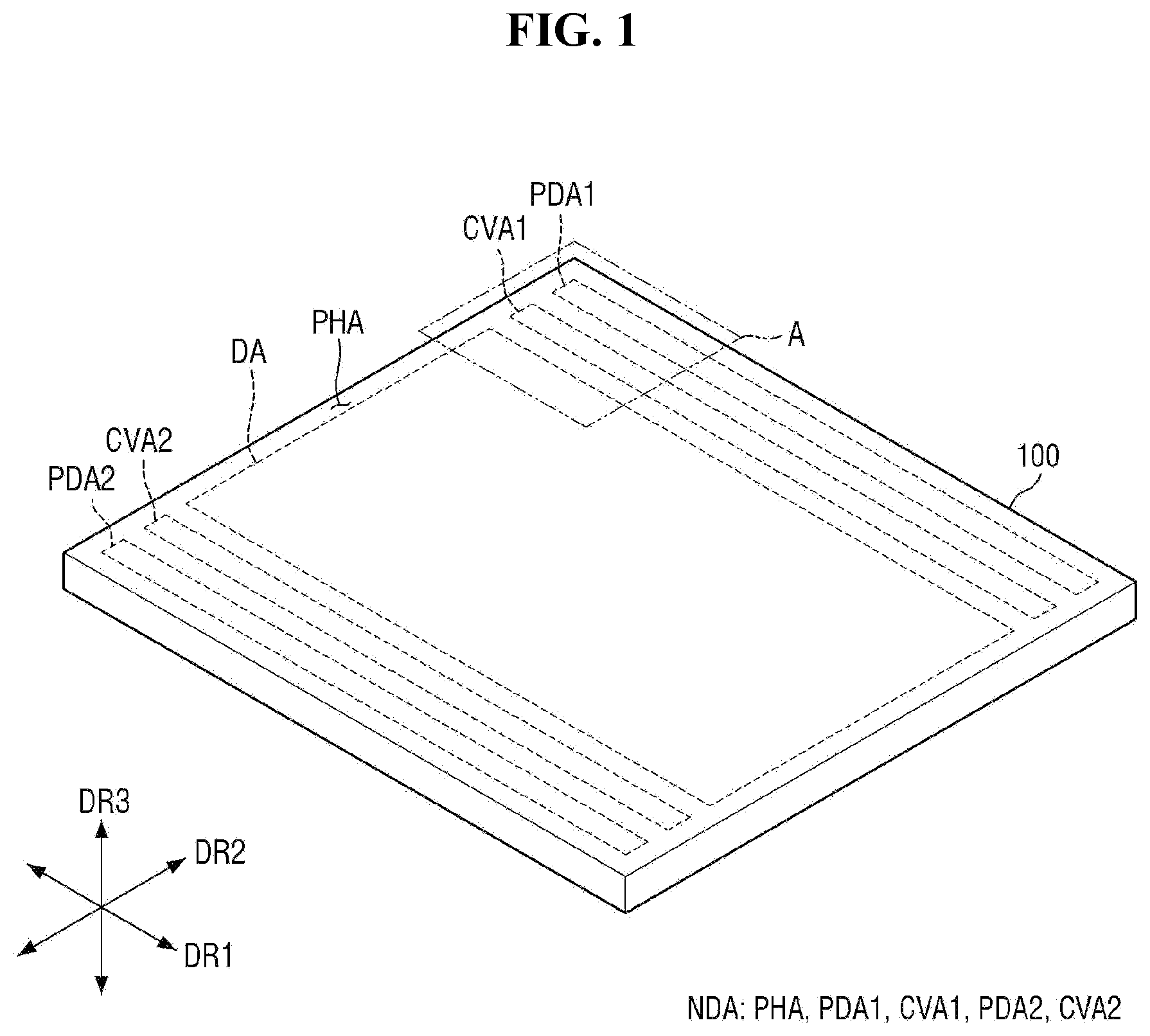
is a layout view of a display device according to an embodiment. is a detailed layout view of the area A of . is a layout view illustrating pixels PX of the display panel according to an embodiment.
In through 3 , the display device is primarily described as an ultra-small light emitting diode display (e.g., a micro-light emitting diode display) including an ultra-small light emitting diode (e.g., a micro-light emitting diode) as a light emitting element, but embodiments of the present disclosure are not limited thereto.
In addition, in through 3 , the display device is primarily described as a light emitting diode on silicon (LEDoS) display device in which light emitting diodes are disposed as light emitting elements on a semiconductor circuit board formed by using a semiconductor process. However, it should be noted that embodiments of the present disclosure are not limited thereto.
In addition, in through 3 , a first direction DR 1 refers to a horizontal direction of the display panel, a second direction DR 2 refers to a vertical direction (in a plan view) of the display panel, and a third direction DR 3 refers to a thickness direction of the display panel or a thickness direction of the semiconductor circuit board. Herein, “left,” “right,” “upper,” and “lower” refer to directions when the display panel is viewed in a plan view. For example, a “right side” refers to one side in the first direction DR 1 , a “left side” refers to the other side in the first direction DR 1 , an “upper side” refers to one side in the second direction DR 2 , and a “lower side” refers to the other side in the second direction DR 2 . In addition, “top” refers to one side in the third direction DR 3 , and “bottom” refers to the other side in the third direction DR 3 .
Referring to through 3 , the display device according to an embodiment includes a display panel 100 having a display area DA and a non-display area NDA.
The display panel 100 may have a quadrilateral planar shape having long sides in the first direction DR 1 and short sides in the second direction DR 2 . However, the planar shape of the display panel 100 is not limited thereto, and the display panel 100 may also have a polygonal, circular, oval, or irregular planar shape other than the quadrilateral shape.
The display area DA may be an area where an image is displayed (e.g., is to be displayed), and the non-display area NDA may be an area where no image is displayed. The planar shape of the display area DA may follow the planar shape of the display panel 100 . In , the planar shape of the display area DA is a quadrilateral shape. The display area DA may be disposed in a central area of the display panel 100 . The non-display area NDA may be disposed around (e.g., around a periphery of) the display area DA. The non-display area NDA may surround (e.g., may surround in a plan view or may extend around a periphery of) the display area DA.
The display area DA of the display panel 100 may include a plurality of pixels PX. Each of the pixels PX may be defined as a minimum light emitting unit that can display white light.
Each of the pixels PX may include a plurality of light emitting areas EA 1 through EA 4 . In an embodiment of the present disclosure, each of the pixels PX includes four light emitting areas EA 1 through EA 4 , but embodiments of the present disclosure are not limited thereto.
Each of the light emitting areas EA 1 through EA 4 may include a light emitting element to emit light. Although each of the light emitting areas EA 1 through EA 4 is illustrated as having a circular planar shape, embodiments of the present disclosure are not limited thereto. For example, each of the light emitting areas EA 1 through EA 4 may also have a polygonal, oval, or irregular planar shape.
Each of first light emitting areas EA 1 refers to an area that emits first light. Each of the first light emitting areas EA 1 may output the first light emitted from a first light emitting element LE 1 as it is (e.g., without modification or variation to the emitted wavelength). The first light may be light in a blue wavelength band. The blue wavelength band may be in a range from about 370 nm to about 460 nm, but embodiments of the present disclosure are not limited thereto.
Each of second light emitting areas EA 2 refers to an area that emits second light. Each of the second light emitting areas EA 2 may output the second light emitted from a second light emitting element LE 2 as it is. The second light may be light in a green wavelength band. The green wavelength band may be in a range from about 480 nm to about 560 nm, but embodiments of the present disclosure are not limited thereto.
Each of third light emitting areas EA 3 refers to an area that emits third light. Each of the third light emitting areas EA 3 may convert a portion of the first light emitted from a third light emitting element LE 3 into the third light and output the third light. The third light may be light in a red wavelength band. The red wavelength band may be in a range from about 600 nm to about 750 nm, but embodiments of the present disclosure are not limited thereto.
Each of fourth light emitting areas EA 4 refers to an area that emits the second light. Each of the fourth light emitting areas EA 4 may output the second light emitted from a fourth light emitting element LE 4 as it is.
In the display area DA, the first light emitting areas EA 1 and the third light emitting areas EA 3 may be alternately disposed in the first direction DR 1 . In the display area DA, the second light emitting areas EA 2 and the fourth light emitting areas EA 4 may be alternately disposed in the second direction DR 2 .
In the display area DA, the first light emitting areas EA 1 , the second light emitting areas EA 2 , the third light emitting areas EA 3 , and the fourth light emitting areas EA 4 may be alternately disposed in a first diagonal direction DD 1 and a second diagonal direction DD 2 . The first diagonal direction DD 1 may be a diagonal direction between the first direction DR 1 and the second direction DR 2 , and the second diagonal direction DD 2 may be a direction crossing (or orthogonal to) the first diagonal direction DD 1 .
In each of the pixels PX, the first light emitting area EA 1 and the third light emitting area EA 3 may be disposed in the first direction DR 1 , and the second light emitting area EA 2 and the fourth light emitting area EA 4 may be disposed in the second direction DR 2 . In each of the pixels PX, the first light emitting area EA 1 and the second light emitting area EA 2 may be disposed in the first diagonal direction DD 1 , the second light emitting area EA 2 and the third light emitting area EA 3 may be disposed in the second diagonal direction DD 2 , and the third light emitting area EA 3 and the fourth light emitting area EA 4 may be disposed in the first diagonal direction DD 1 .
The area of the first light emitting area EA 1 , the area of the second light emitting area EA 2 , the area of the third light emitting area EA 3 , and the area of the fourth light emitting area EA 4 may be substantially the same, but embodiments of the present disclosure are not limited thereto. For example, the area of the second light emitting area EA 2 and the area of the fourth light emitting area EA 4 may be substantially the same, but the area of the first light emitting area EA 1 may be smaller than the area of the second light emitting area EA 2 , and the area of the third light emitting area EA 3 may be larger than the area of the second light emitting area EA 2 . In other embodiments, the area of the second light emitting area EA 2 and the area of the fourth light emitting area EA 4 may be substantially the same, but the area of the third light emitting area EA 3 may be smaller than the area of the second light emitting area EA 2 , and the area of the first light emitting area EA 1 may be larger than the area of the second light emitting area EA 2 .
In addition, a minimum distance D 12 between the first light emitting area EA 1 and the second light emitting area EA 2 neighboring each other, a minimum distance D 23 between the second light emitting area EA 2 and the third light emitting area EA 3 neighboring each other, a minimum distance D 14 between the first light emitting area EA 1 and the fourth light emitting area EA 4 neighboring each other, and a minimum distance D 34 between the third light emitting area EA 3 and the fourth light emitting area EA 4 neighboring each other may be substantially the same, but embodiments of the present disclosure are not limited thereto. For example, the minimum distance D 12 between the first light emitting area EA 1 and the second light emitting area EA 2 neighboring each other and the minimum distance D 23 between the second light emitting area EA 2 and the third light emitting area EA 3 neighboring each other may be different, and the minimum distance D 14 between the first light emitting area EA 1 and the fourth light emitting area EA 4 neighboring each other and the minimum distance D 34 between the third light emitting area EA 3 and the fourth light emitting area EA 4 neighboring each other may be different. In such an embodiment, the minimum distance D 12 between the first light emitting area EA 1 and the second light emitting area EA 2 neighboring each other and the minimum distance D 14 between the first light emitting area EA 1 and the fourth light emitting area EA 4 neighboring each other may be substantially the same, and the minimum distance D 23 between the second light emitting area EA 2 and the third light emitting area EA 3 neighboring each other and the minimum distance D 34 between the third light emitting area EA 3 and the fourth light emitting area EA 4 neighboring each other may be substantially the same.
In addition, the first light emitting area EA 1 may emit the first light, the second light emitting area EA 2 and the fourth light emitting area EA 4 may emit the second light, and the third light emitting area EA 3 may emit the third light, but embodiments of the present disclosure area not limited thereto. For example, the first light emitting area EA 1 may emit the first light, the second light emitting area EA 2 and the fourth light emitting area EA 4 may emit the third light, and the third light emitting area EA 3 may emit the second light. In other embodiments, the first light emitting area EA 1 may emit the second light, the second light emitting area EA 2 and the fourth light emitting area EA 4 may emit the first light, and the third light emitting area EA 3 may emit the third light. In other embodiments, the first light emitting area EA 1 may emit the first light, the second light emitting area EA 2 may emit the second light, the third light emitting area EA 3 may emit the third light, and the fourth light emitting area EA 4 may emit fourth light. The fourth light may be light in a yellow wavelength band. That is, a primary peak wavelength of the fourth light may be in a range from about 550 nm to about 600 nm, but embodiments of the present disclosure are not limited thereto.
The display area DA of the display panel 100 may further include a partition wall portion PW that separates the light emitting areas EA 1 through EA 4 . The partition wall portion PW may include a plurality of partition walls.
The non-display area NDA may include common voltage supply units CVS, a first pad portion PDA 1 , and a second pad portion PDA 2 .
The first pad portion PDA 1 may be disposed on an upper side of the display panel 100 . The first pad portion PDA 1 may include first pads PD 1 connected to an external circuit board.
The second pad portion PDA 2 may be disposed on a lower side of the display panel 100 . The second pad portion PDA 2 may include second pads PD 2 so as to be connected to an external circuit board. In some embodiments, the second pad portion PDA 2 may be omitted.
The common voltage supply units CVS may be disposed between the first pad portion PDA 1 and the display area DA. In addition, the common voltage supply units CVS may be disposed between the second display portion PDA 2 and the display area DA. The common voltage supply units CVS may be connected to a common electrode. Therefore, a common voltage of the common voltage supply units CVS may be supplied to the common electrode. The common voltage supply units CVS may be electrically connected to any one of the first pads PD 1 of the first pad portion PDA 1 . In some embodiments, the common voltage supply units CVS may be electrically connected to any one of the second pads PD 2 of the second pad portion PDA 2 .
is a layout view of the area A of according to another embodiment.
In , different from the embodiment shown in , each of a plurality of pixels PX includes three light emitting areas EA 1 through EA 3 . In describing the embodiment shown in , differences from the embodiment shown in will be primarily described.
Referring to , first light emitting areas EA 1 , second light emitting areas EA 2 , and third light emitting areas EA 3 may be alternately arranged in the first direction DR 1 . For example, the first light emitting areas EA 1 , the second light emitting areas EA 2 , and the third light emitting areas EA 3 may be disposed in the order of the first light emitting area EA 1 , the second light emitting area EA 2 , and the third light emitting area EA 3 in the first direction DR 1 . In addition, in each of the pixels PX, the first light emitting area EA 1 , the second light emitting area EA 2 , and the third light emitting area EA 3 may be arranged in the first direction DR 1 .
The first light areas EA 1 may be arranged in the second direction DR 2 . The second light emitting areas EA 2 may be arranged in the second direction DR 2 . The third light emitting areas EA 3 may be arranged in the second direction DR 2 .
is a cross-sectional view of the display panel 100 taken along the line A-A′ of according to an embodiment. is a cross-sectional view of an example of the area B of . is an enlarged cross-sectional view illustrating a first light emitting element LE 1 , a second light emitting element LE 2 , a third light emitting element LE 3 , and a fourth light emitting element LE 4 shown in in detail.
Referring to through 7 , the display panel 100 may include the semiconductor circuit board 110 and a light emitting element layer 120 .
The semiconductor circuit board 110 may include a first substrate SUB 1 , a plurality of pixel circuit units PXC, and pixel electrodes PXE 1 through PXE 4 .
The first substrate SUB 1 may be a silicon wafer substrate. The first substrate SUB 1 may be made of monocrystalline silicon.
Each of the pixel circuit units PXC may be disposed on the first substrate SUB 1 . Each of the pixel circuit units PXC may include a complementary metal oxide semiconductor (CMOS) circuit formed by using a semiconductor process. Each of the pixel circuit units PXC may include at least one transistor formed by using a semiconductor process. In addition, each of the pixel circuit units PXC may further include at least one capacitor formed by using a semiconductor process.
The pixel circuit units PXC may be disposed in the display area DA. Each of the pixel circuit units PXC may be connected to a corresponding pixel electrode PXE 1 /PXE 2 /PXE 3 /PXE 4 from among the pixel electrodes PXE 1 through PXE 4 . For example, the pixel circuit units PXC and the pixel electrodes PXE 1 through PXE 4 may be connected to each other in a one-to-one manner. Each of the pixel circuit units PXC may apply a pixel voltage (or an anode voltage) to a corresponding pixel electrode PXE 1 /PXE 2 /PXE 3 /PXE 4 .
Each of the pixel electrodes PXE 1 through PXE 4 may be disposed on a corresponding pixel circuit unit PXC. Each of the pixel electrodes PXE 1 through PXE 4 may be an exposed electrode exposed from the pixel circuit unit PXC. For example, each of the pixel electrodes PXE 1 through PXE 4 may protrude from an upper surface of the pixel circuit unit PXC. Each of the pixel electrodes PXE 1 through PXE 4 may be integrally formed with the pixel circuit unit PXC. Each of the pixel electrodes PXE 1 through PXE 4 may receive a pixel voltage (or an anode voltage) from the pixel circuit unit PXC. The pixel electrodes PXE 1 through PXE 4 may be made of aluminum (Al). However, embodiments of the present disclosure are not limited thereto, and the pixel electrodes PXE 1 through PXE 4 may also be made of another metal.
Each of first pixel electrodes PXE 1 may be disposed in a corresponding first light emitting area EA 1 . Each of second pixel electrodes PXE 2 may be disposed in a corresponding second light emitting area EA 2 . Each of third pixel electrodes PXE 3 may be disposed in a corresponding third light emitting area EA 3 . Each of fourth pixel electrodes PXE 4 may be disposed in a corresponding fourth light emitting area EA 4 .
The light emitting element layer 120 may be a layer including the light emitting elements LE 1 through LE 4 to emit light (e.g., predetermined light). The light emitting element layer 120 may include first conductive layers CL 1 , second conductive layers CL 2 , first connection electrodes BE 1 , the light emitting elements LE 1 through LE 4 , a common electrode CE, a first insulating layer INS 1 , a second insulating layer INS 2 , a third insulating layer INS 3 , a planarization layer PNL, a first wavelength conversion layer QDL 1 , a first color filter CF 1 , and a partition wall portion PW. The partition wall portion PW may include a first partition wall PW 1 and a second partition wall PW 2 .
Each of the first conductive layers CL 1 may be disposed on a corresponding pixel electrode PXE 1 /PXE 2 /PXE 3 /PXE 4 . The first conductive layers CL 1 may be bonding metal layers for bonding the pixel electrodes PXE 1 through PXE 4 to the light emitting elements LE. For example, each of the first conductive layers CL 1 may include at least any one of gold (Au), copper (Cu), aluminum (Al), and tin (Sn). In another embodiment, each of the first conductive layers CL 1 may include a first layer including any one of gold (Au), copper (Cu), aluminum (Al) and tin (Sn) and a second layer including another one of gold (Au), copper (Cu), aluminum (Al) and tin (Sn). In such an embodiment, the second layer may be disposed on the first layer.
The light emitting element layer 120 may include the first light emitting areas EA 1 , the second light emitting areas EA 2 , the third light emitting areas EA 3 , and the fourth light emitting areas EA 4 separated by the partition wall portion PW. The first light emitting element LE 1 may be disposed in each of the first light emitting areas EA 1 , the second light emitting element LE 2 may be disposed in each of the second light emitting areas EA 2 , the third light emitting element LE 3 may be disposed in each of the third light emitting areas EA 3 , and the fourth light emitting element LE 4 may be disposed in each of the fourth light emitting areas EA 4 .
Each of the first light emitting element LE 1 , the second light emitting element LE 2 , the third light emitting element LE 3 , and the fourth light emitting element LE 4 may be a vertical light emitting diode element extending in the third direction DR 3 . For example, a length of each of the first light emitting element LE 1 , the second light emitting element LE 2 , the third light emitting element LE 3 , and the fourth light emitting element LE 4 in the third direction DR 3 may be greater than a length thereof in the horizontal direction. The length in the horizontal direction refers to a length in the first direction DR 1 or a length in the second direction DR 2 . For example, the length of each of the first light emitting element LE 1 , the second light emitting element LE 2 , the third light emitting element LE 3 , and the fourth light emitting element LE 4 in the third direction DR 3 may be about 1 μm to 5 μm.
Each of the first light emitting element LE 1 , the second light emitting element LE 2 , the third light emitting element LE 3 , and the fourth light emitting element LE 4 may be a micro-light emitting diode element. The first light emitting element LE 1 and the third light emitting element LE 3 may be substantially the same, and the second light emitting element LE 2 and the fourth light emitting element LE 4 may be substantially the same.
Each of the first light emitting element LE 1 and the third light emitting element LE 3 may include a first semiconductor layer SEM 1 , an electron blocking layer EBL, a first active layer MQW 1 , a superlattice layer SLT, and a second semiconductor layer SEM 2 as illustrated in . Each of the second light emitting element LE 2 and the fourth light emitting element LE 4 may include a first semiconductor layer SEM 1 , an electron blocking layer EBL, a second active layer MQW 2 , a superlattice layer SLT, and a second semiconductor layer SEM 2 as illustrated in, for example, . The first semiconductor layer SEM 1 , the electron blocking layer EBL, the first active layer MQW 1 or the second active layer MQW 2 , the superlattice layer SLT, and the second semiconductor layer SEM 2 may be sequentially stacked in the third direction DR 3 .
The first semiconductor layer SEM 1 may be disposed on a first conductive layer CL 1 . The first semiconductor layer SEM 1 may be doped with a dopant of a first conductive type, such as Mg, Zn, Ca, Se, or Ba. For example, the first semiconductor layer SEM 1 may be p-GaN doped with p-type Mg. A thickness Tsem 1 of the first semiconductor layer SEM 1 may be in a range of about 30 nm to about 200 nm.
The electron blocking layer EBL may be disposed on the first semiconductor layer SEM 1 . The electron blocking layer EBL may be a layer for suppressing (or preventing) too many electrons from flowing into the first active layer MQW 1 or the second active layer MQW 2 . For example, the electron blocking layer EBL may be p-AlGaN doped with p-type Mg. A thickness Tebl of the electron blocking layer EBL may be in a range of about 10 nm to about 50 nm. In some embodiments, the electron blocking layer EBL may be omitted.
The first active layer MQW 1 may be disposed on the electron blocking layer EBL in each of the first light emitting element LE 1 and the third light emitting element LE 3 . The first active layer MQW 1 may emit light through the combination of electron-hole pairs according to an electrical signal received though the first semiconductor layer SEM 1 and the second semiconductor layer SEM 2 . The first active layer MQW 1 may emit the first light, that is, light in the blue wavelength band.
The second active layer MQW 2 may be disposed on the electron blocking layer EBL in each of the second light emitting element LE 2 and the fourth light emitting element LE 4 . The second active layer MQW 2 may emit light through combination of electron-hole pairs according to an electrical signal received though the first semiconductor layer SEM 1 and the second semiconductor layer SEM 2 . The second active layer MQW 2 may emit the second light, that is, light in the green wavelength band.
Each of the first active layer MQW 1 and the second active layer MQW 2 may include a material having a single or multiple quantum well structure. When each of the first active layer MQW 1 and the second active layer MQW 2 includes a material having a multiple quantum well structure, it may have a structure in which a plurality of well layers and a plurality of barrier layers are alternately stacked. In some embodiments, the well layers may be made of InGaN and the barrier layers may be made of GaN or AlGaN, but embodiments of the present disclosure are not limited thereto. The well layers may have a thickness in a range of about 1 nm to about 4 nm, and the barrier layers may have a thickness in a range of about 3 nm to about 10 nm.
Alternatively, each of the first active layer MQW 1 and the second active layer MQW 2 may have a structure in which a semiconductor material having a large band gap energy and a semiconductor material having a small band gap energy are alternately stacked or may include different Group 3 to 5 semiconductor materials depending on the wavelength band of light to be emitted.
When each of the first active layer MQW 1 and the second active layer MQW 2 includes InGaN, the color of emitted light may vary according to the content of indium (In). As the indium content increases, the wavelength band of light emitted from an active layer may move toward the red wavelength band. As the indium content decreases, the wavelength band of light emitted from the active layer may move toward the blue wavelength band. Therefore, the indium content of the first active layer MQW 1 may be lower than the indium content of the second active layer MQW 2 . For example, the indium content of the first active layer MQW 1 may be in a range of about 10 wt % to about 20 wt %, and the indium content of the second active layer MQW 2 may be in a range of about 20 wt % to about 30 wt %. In such an embodiment, the first active layer MQW 1 may emit the first light, and the second active layer MQW 2 may emit the second light.
The superlattice layer SLT may be disposed on each of the first active layer MQW 1 and the second active layer MQW 2 . The superlattice layer SLT may be a layer for relieving stress between the second semiconductor layer SEM 2 and the first active layer MQW 1 or the second active layer MQW 2 . For example, the superlattice layer SLT may be made of InGaN or GaN. A thickness Tslt of the superlattice layer SLT may be in a range of about 50 nm to about 200 nm. In some embodiments, the superlattice layer SLT may be omitted.
The second semiconductor layer SEM 2 may be disposed on the superlattice layer SLT. The second semiconductor layer SEM 2 may be doped with a dopant of a second conductivity type, such as Si, Ge, or Sn. For example, the second semiconductor layer SEM 2 may be n-GaN doped with n-type Si. A thickness Tsem 2 of the second semiconductor layer SEM 2 may be in a range of about 2 μm to about 4 μm.
The first light emitting element LE 1 may be disposed on the first conductive layer CL 1 in each of the first light emitting areas EA 1 . The third light emitting element LE 3 may be disposed on the first conductive layer CL 1 in each of the third light emitting areas EA 3 .
The first connection electrode BE 1 may be disposed on the first conductive layer CL 1 in each of the second light emitting areas EA 2 and the fourth light emitting areas EA 4 . The first connection electrode BE 1 may be made of a metal material having high conductivity. For example, the first connection electrode BE 1 may be made of a metal material, such as molybdenum (Mo), aluminum (Al), chromium (Cr), gold (Au), tin (Sn), titanium (Ti), nickel (Ni), neodymium (Nd), or copper (Cu). A thickness Tle 1 of the first light emitting element LE 1 , a thickness Tle 3 of the third light emitting element LE 3 , and a thickness Tbe 1 of the first connection electrode BE 1 may be substantially the same. The thickness Tle 1 of the first light emitting element LE 1 refers to the length of the first light emitting element LE 1 in the third direction DR 3 .
The first insulating layer INS 1 may be disposed on side surfaces of each of the first and third light emitting elements LE 1 and LE 3 . The first insulating layer INS 1 may not be disposed on an upper surface of each of the first and third light emitting elements LE 1 and LE 3 . In addition, the first insulating layer INS 1 may be disposed on side surfaces of each of the pixel electrodes PXE 1 through PXE 4 and the first conductive layers CL 1 . In addition, the first insulating layer INS 1 may be disposed on part of side surfaces of each of the first connection electrodes BE 1 .
In addition, the first insulating layer INS 1 may be disposed on the first substrate SUB 1 . In other embodiments, the first insulating layer INS 1 disposed on the first substrate SUB 1 may be omitted.
The first insulating layer INS 1 may be formed of an inorganic layer, such as a silicon oxide (e.g., SiO 2 ) layer, an aluminum oxide (e.g., Al 2 O 3 ) layer, or a hafnium oxide (HfO x ) layer, but embodiments of the present disclosure are not limited thereto.
The first partition wall PW 1 may be disposed on the side surfaces of each of the first and third light emitting elements LE 1 and LE 3 . The first partition wall PW 1 may surround the side surfaces of each of the first and third light emitting elements LE 1 and LE 3 . The first partition wall PW 1 may be disposed on the side surfaces of each of the first connection electrodes BE 1 . The first partition wall PW 1 may surround the side surfaces of each of the first connection electrode BE 1 .
The first partition wall PW 1 may be disposed on the first insulating layer INS 1 . Side surfaces of the first partition wall PW 1 may contact the first insulating layer INS 1 disposed on the side surfaces of each of the first and third light emitting elements LE 1 and LE 3 and the first connection electrodes BE 1 . A lower surface of the first partition wall PW 1 may contact the first insulating layer INS 1 disposed on the first substrate SUB 1 . In other embodiments in which the first insulating layer INS 1 disposed on the first substrate SUB 1 is omitted, the lower surface of the first partition wall PW 1 may contact the first substrate SUB 1 .
An upper surface of the first partition wall PW 1 , an upper surface of the first insulating layer INS 1 , the upper surface of the first light emitting element LE 1 , the upper surface of the third light emitting element LE 3 , and upper surfaces of the first connection electrodes BE 1 may be connected (e.g., may be directly adjacent to each other without a gap therebetween) to form a flat surface. While the first insulating layer INS 1 is disposed between the first partition wall PW 1 and the first substrate SUB 1 , the first pixel electrode PXE 1 and the first conductive layer CL 1 are disposed between the first light emitting element LE 1 and the first substrate SUB 1 . Therefore, a thickness Tpw 1 of the first partition wall PW 1 may be greater than the thickness Tle 1 of the first light emitting element LE 1 .
The first partition wall PW 1 may include a material having conductivity (e.g., a conductive material). For example, the first partition wall PW 1 may be made of a metal material having high thermal conductivity. In such an embodiment, heat generated by the first and third light emitting elements LE 1 and LE 3 may be radiated to the first partition wall PW 1 . For example, the first partition wall PW 1 may dissipate heat generated by the first and third light emitting elements LE 1 and LE 3 .
In addition, the first partition wall PW 1 may include a metal material having high reflectivity. In such an embodiment, the first light emitted from the first light emitting element LE 1 may be reflected upwardly above the first light emitting element LE 1 by the first partition wall PW 1 . In addition, the first light emitted from the third light emitting element LE 3 may be reflected upwardly above the third light emitting element LE 3 by the first partition wall PW 1 . Therefore, the output efficiency of the first light of the first light emitting element LE 1 and the output efficiency of the first light of the third light emitting element LE 3 may be increased by the first partition wall PW 1 .
The first partition wall PW 1 may be made of aluminum (Al). However, embodiments of the present disclosure are not limited thereto, and the first partition wall PW 1 may also be made of an opaque metal material, such as molybdenum (Mo), chromium (Cr), gold (Au), titanium (Ti), nickel (Ni), neodymium (Nd), or copper (Cu).
A first oxide layer PWO 1 , formed by oxidizing the upper surface of the first partition wall PW 1 , may be formed on the upper surface of the first partition wall PW 1 as illustrated in, for example, . For example, when the first partition wall PW 1 is made of aluminum (Al), the first oxide layer PWO 1 may be an aluminum oxide (e.g., Al 2 O 3 ) layer. The first partition wall PW 1 may be electrically insulated from the common electrode CE by the first oxide layer PWO 1 .
The second conductive layers CL 2 may be disposed on the first connection electrodes BE 1 , respectively. The second conductive layers CL 2 may be bonding metal layers for bonding the first connection electrodes BE 1 to the second light emitting elements LE 2 or the fourth light emitting elements LE 4 . For example, each of the second conductive layers CL 2 may include at least any one of gold (Au), copper (Cu), aluminum (Al), and tin (Sn). In some embodiments, each of the second conductive layers CL 2 may include a first layer including any one of gold (Au), copper (Cu), aluminum (Al), and tin (Sn) and a second layer including another one of gold (Au), copper (Cu), aluminum (Al)m and tin (Sn). In such an embodiment, the second layer may be disposed on the first layer.
The second light emitting element LE 2 may be disposed on the second conductive layer CL 2 in each of the second light emitting areas EA 2 , and the fourth light emitting element LE 4 may be disposed on the second conductive layer CL 2 in each of the second light emitting areas EA 2 .
For example, a minimum distance between the second light emitting element LE 2 and the first substrate SUB 1 and a minimum distance between the fourth light emitting element LE 4 and the first substrate SUB 1 may be greater than a minimum distance between the first light emitting element LE 1 and the first substrate SUB 1 and a minimum distance between the third light emitting element LE 3 and the first substrate SUB 1 . The minimum distance between the first light emitting element LE 1 and the first substrate SUB 1 and the minimum distance between the third light emitting element LE 3 and the first substrate SUB 1 may be substantially the same. The minimum distance between the second light emitting element LE 2 and the first substrate SUB 1 and the minimum distance between the fourth light emitting element LE 4 and the first substrate SUB 1 may be substantially the same.
The second insulating layer INS 2 may be disposed on side surfaces of each of the second and fourth light emitting elements LE 2 and LE 4 . The second insulating layer INS 2 may not be disposed on an upper surface of each of the second and fourth light emitting elements LE 2 and LE 4 . In addition, the second insulating layer INS 2 may be disposed on side surfaces of each of the second conductive layers CL 2 . In addition, the second insulating layer INS 2 may be disposed on the first partition wall PW 1 . The second insulating layer INS 2 may be formed of an inorganic layer, such as a silicon oxide (e.g., SiO 2 ) layer, an aluminum oxide (e.g., Al 2 O 3 ) layer, or a hafnium oxide (HfO x ) layer, but embodiments of the present disclosure are not limited thereto.
The common electrode CE may be disposed on the upper surface of each of the light emitting elements LE 1 through LE 4 , an upper surface of the second insulating layer INS 2 , and the upper surface of the first partition wall PW 1 . The common electrode CE may be disposed on the side surfaces of each of the second and fourth light emitting elements LE 2 and LE 4 . The common electrode CE may include a transparent conductive material. For example, the common electrode CE may include a transparent conductive oxide (TCO), such as indium tin oxide (ITO) or indium zinc oxide (IZO).
The planarization layer PNL may be disposed on the common electrode CE in each of the first light emitting areas EA 1 . The planarization layer PNL may overlap the first light emitting element LE 1 in the third direction DR 3 . The common electrode CE may be disposed between the first light emitting element LE 1 and the planarization layer PNL in each of the first light emitting areas EA 1 . The planarization film PNL may be formed of an organic layer, such as acryl resin, epoxy resin, phenolic resin, polyamide resin, or polyimide resin.
The first wavelength conversion layer QDL 1 may be disposed on the common electrode CE in each of the third light emitting areas EA 3 . The first wavelength conversion layer QDL 1 may overlap the third light emitting element LE 3 . The common electrode CE may be disposed between the third light emitting element LE 3 and the first wavelength conversion layer QDL 1 in each of the third light emitting areas EA 3 .
The first wavelength conversion layer QDL 1 may convert a portion of (or some of) the first light of (e.g., emitted by) the third light emitting element LE 3 into the third light and output the third light. The first wavelength conversion layer QDL 1 may include a first base resin BRS 1 and first wavelength conversion particles WCP 1 .
The first base resin BRS 1 may include a light-transmitting organic material. For example, the first base resin BRS 1 may include epoxy resin, acrylic resin, cardo resin, or imide resin.
The first wavelength conversion particles WCP 1 may convert the first light of the third light emitting element LE 3 into the third light. For example, the first wavelength conversion particles WCP 1 may convert light of the blue wavelength band into light of the red wavelength band. The first wavelength conversion particles WCP 1 may be quantum dots, quantum rods, a fluorescent material, or a phosphorescent material. The quantum dots may include Group IV nanocrystals, Group II-VI compound nanocrystals, Group III-V compound nanocrystals, Group IV-VI nanocrystals, or a combination thereof.
Each quantum dot may include a core and a shell over-coating the core. The core may be, but is not limited to, at least one of, for example, CdS, CdSe, CdTe, ZnS, ZnSe, ZnTe, GaN, GaP, GaAs, GaSb, AlN, AlP, AlAs, AlSb, InP, InAs, InSb, SiC, Ca, Se, In, P, Fe, Pt, Ni, Co, Al, Ag, Au, Cu, FePt, Fe 2 O 3 , Fe 3 O 4 , Si, and Ge. The shell may include, but is not limited to, at least one of, for example, ZnS, ZnSe, ZnTe, CdS, CdSe, CdTe, HgS, HgSe, HgTe, AlN, AlP, AlAs, AlSb, GaN, GaP, GaAs, GaSb, GaSe, InN, InP, InAs, InSb, TlN, TlP, TlAs, TlSb, PbS, PbSe, and PbTe.
The first wavelength conversion layer QDL 1 may further include scatterers for scattering the first light of the third light emitting element LE 3 in various directions. The scatterers may include metal oxide particles or organic particles. For example, the metal oxide may be titanium oxide (e.g., TiO 2 ), zirconium oxide (e.g., ZrO 2 ), silicon dioxide (SiO 2 ), aluminum oxide (e.g., Al 2 O 3 ), indium oxide (e.g., In 2 O 3 ), zinc oxide (ZnO), or tin oxide (e.g., SnO 2 ). In addition, the organic particles may include acrylic resin or urethane resin. A diameter of the scatterers may be in a range of several nanometers to several tens of nanometers.
The second partition wall PW 2 may be disposed on the side surfaces of each of the second and fourth light emitting elements LE 2 and LE 4 , the planarization layer PNL, and the first wavelength conversion layer QDL 1 . The second partition wall PW 2 may surround the side surfaces of each of the second and fourth light emitting elements LE 2 and LE 4 , the planarization layer PNL, and the first wavelength conversion layer QDL 1 .
The second partition wall PW 2 may be disposed on the second insulating layer INS 2 . Side surfaces of the second partition wall PW 2 may contact the second insulating layer INS 2 disposed on the side surfaces of each of the second and fourth light emitting elements LE 2 and LE 4 . A lower surface of the second partition wall PW 2 may contact the first partition wall PW 1 and the first insulating layer INS 1 disposed on the first partition wall PW 1 . An upper surface of the second partition wall PW 2 , an upper surface of the common electrode CE, an upper surface of the planarization layer PNL, and an upper surface of the first wavelength conversion layer QLD 1 may be connected to form a flat surface.
The second partition wall PW 2 may include a material having conductivity (e.g., a conductive material). For example, the second partition wall PW 2 may be made of a metal material having high thermal conductivity. In such an embodiment, heat generated by the second and fourth light emitting elements LE 2 and LE 4 may be radiated to the second partition wall PW 2 . For example, the second partition wall PW 2 may dissipate heat generated by the second and fourth light emitting elements LE 2 and LE 4 .
In addition, the second partition wall PW 2 may include a metal material having high reflectivity. The second partition wall PW 2 may be made of aluminum (Al). However, embodiments of the present disclosure are not limited thereto, and the second partition wall PW 2 may also be made of an opaque metal material, such as molybdenum (Mo), chromium (Cr), gold (Au), titanium (Ti), nickel (Ni), neodymium (Nd), or copper (Cu).
When the second partition wall PW 2 is made of a metal material having high reflectivity, the first light emitted from the first light emitting element LE 1 may be reflected upwardly above the planarization layer PNL by the second partition wall PW 2 . In addition, the second light emitted from the second light emitting element LE 2 and the second light emitted from the fourth light emitting element LE 4 may be reflected upwardly above the second light emitting element LE 2 and the fourth light emitting element LE 4 by the second partition wall PW 2 . Therefore, the second partition wall PW 2 may increase (or improve) the output efficiency (e.g., the light output or emission efficiency) of the first light of the first light emitting element LE 1 , the output efficiency of the second light of the second light emitting element LE 2 , and the output efficiency of the second light of the fourth light emitting element LE 4 .
Further, when the second partition wall PW 2 is made of a metal material having high reflectivity, the first light emitted from the third light emitting element LE 3 may be reflected by the second partition wall PW 2 to re-enter the first wavelength conversion layer QDL 1 . Therefore, a conversion ratio of the first light emitted from the third light emitting element LE 3 to the third light may be increased.
In other embodiments, the second partition wall PW 2 may include a light blocking material that absorbs or blocks light. The light blocking material may be an inorganic black pigment, such as carbon black or an organic black pigment. In such an embodiment, the second partition wall PW 2 may prevent light emitted from adjacent light emitting elements LE 1 through LE 4 from being mixed with each other.
The first color filter CF 1 may be disposed on the first wavelength conversion layer QDL 1 in each of the third light emitting areas EA 3 . The first color filter CF 1 may transmit the third light into which the first light of the third light emitting element ED 3 has been converted by the first wavelength conversion layer QDL 1 and may absorb or block the first light of the third light emitting element LE 3 that is not converted by the first wavelength conversion layer QDL 1 . For example, the first color filter CF 1 may transmit light of the red wavelength band and may absorb or block light of the blue wavelength band. Therefore, each of the third light emitting areas EA 3 may emit the third light.
The third insulating layer INS 3 may be disposed on an upper surface of the first color filter CF 1 , the upper surface of the second partition wall PW 2 , the upper surface of the common electrode CE, and the upper surface of the planarization layer PNL. The third insulating layer INS 3 may be disposed on side surfaces of the first color filter CF 1 . The third insulating layer INS 3 may be formed of an inorganic layer, such as a silicon oxide (e.g., SiO 2 ) layer, an aluminum oxide (e.g., Al 2 O 3 ) layer, or a hafnium oxide (HfO x ) layer, but embodiments of the present disclosure are not limited thereto. In some embodiments, the third insulating layer INS 3 may be omitted.
In the embodiment illustrated in through 7 , the first partition wall PW 1 and the second partition wall PW 2 are made of a material having conductivity. Therefore, heat generated by the light emitting elements LE 1 through LE 4 may be radiated to the first partition wall PW 1 and the second partition wall PW 2 .
In addition, the first partition wall PW 1 and the second partition wall PW 2 are made of a metal material having high reflectivity. Therefore, light emitted from each of the light emitting elements LE 1 through LE 4 may be reflected upwardly above each of the light emitting elements LE 1 through LE 4 by the first partition wall PW 1 and the second partition wall PW 2 . Accordingly, the light output efficiency of each of the light emitting elements LE 1 through LE 4 may be increased by the first partition wall PW 1 and the second partition wall PW 2 .
In addition, the second partition wall PW 2 is made of a metal material having high reflectivity. Therefore, the first light of the third light emitting element LE 3 may be reflected by the second partition wall PW 2 to re-enter the first wavelength conversion layer QDL 1 . Accordingly, the output efficiency of the third light of the third light emitting element LE 3 may be increased.
In addition, the luminous efficiency of the first light emitting element LE 1 emitting the first light, the luminous efficiency of the third light emitting element LE 3 emitting the first light, and the luminous efficiency of the second light emitting element LE 2 emitting the second light are higher than the luminous efficiency of a light emitting element emitting the third light. Therefore, the third light emitting element LE 3 emitting the first light may be used instead of the light emitting element emitting the third light and having low luminous efficiency, and the third light may be emitted by using (or by including) the first wavelength conversion layer QDL 1 .
Further, each of the pixels PX includes the first and third light emitting elements LE 1 and LE 3 emitting the first light and the second and fourth light emitting elements LE 2 and LE 4 emitting the second light. Therefore, only the first wavelength conversion layer QDL 1 is included to convert the first light of the third light emitting element LE 3 into the third light. This can facilitate (e.g., improve) a fabrication process.
is a circuit diagram of the first light emitting element LE 1 and the pixel circuit unit PXC shown in according to an embodiment.
Referring to , a pixel circuit unit PXC may include a driving transistor DT, a first transistor ST 1 , a second transistor ST 2 , and a capacitor Cst.
A light emitting element LE emits light according to a driving current. The amount of light emitted from the light emitting element LE may be proportional to the driving current. The light emitting element LE may have an anode connected to a source electrode of the driving transistor DT and a cathode connected to a second power line VSL to which a low potential voltage, lower than a high potential voltage, is supplied.
The driving transistor DT adjusts a current flowing from a first power line VDL, to which a first power supply voltage is supplied, to the light emitting element LE according to a voltage difference between a gate electrode and the source electrode. The gate electrode of the driving transistor DT may be connected to a first electrode of the first transistor ST 1 , the source electrode thereof may be connected to the anode of the light emitting element LE, and a drain electrode thereof may be connected to the second power line VSL to which a high potential voltage is applied.
The first transistor ST 1 is turned on by a scan signal of (or transmitted by) a scan line SL to connect a data line DL to the gate electrode of the driving transistor DT. The first transistor ST 1 may have a gate electrode connected to the scan line SL, the first electrode connected to the gate electrode of the driving transistor DT, and a second electrode connected to the data line DL.
The second transistor ST 2 is turned on by a sensing signal of a sensing signal line SSL to connect an initialization voltage line VIL to the source electrode of the driving transistor DT. The second transistor ST 2 may have a gate electrode connected to the sensing signal line SSL, a first electrode connected to the initialization voltage line VIL, and a second electrode connected to the source electrode of the driving transistor DT.
The first electrode of each of the first and second transistors ST 1 and ST 2 may be a source electrode, and the second electrode may be a drain electrode. However, it should be noted that embodiments of the present disclosure are not limited thereto. For example, the first electrode of each of the first and second transistors ST 1 and ST 2 may also be a drain electrode, and the second electrode may also be a source electrode.
The capacitor Cst is formed between the gate electrode and the source electrode of the driving transistor DT. The storage capacitor Cst stores a difference voltage between a gate voltage and a source voltage of the driving transistor DT.
Although the driving transistor DT and the first and second transistors ST 1 and ST 2 are primarily described as N-type metal oxide semiconductor field effect transistors (MOSFETs) in , it should be noted that embodiments of the present disclosure are not limited thereto. For example, the driving transistor DT and the first and second transistors ST 1 and ST 2 may be formed as P-type MOSFETs.
is a circuit diagram of the first light emitting element LE 1 and the pixel circuit unit PXC shown in according to another embodiment.
Referring to , a pixel circuit unit PXC includes a driving transistor DT, switch elements, and a capacitor C 1 . The switch elements include first through sixth transistors ST 1 through ST 6 .
The driving transistor DT includes a gate electrode, a first electrode, and a second electrode. The driving transistor DT controls a drain-source current (hereinafter, referred to as a “driving current”) flowing between the first electrode and the second electrode according to a data voltage applied to the gate electrode.
The capacitor C 1 is formed between the second electrode of the driving transistor DT and a second power line VSL. The capacitor Cst may have one electrode connected to the second electrode of the driving transistor DT and the other electrode connected to the second power line VSL.
When a first electrode of each of the first through sixth transistors ST 1 through ST 6 and of the driving transistor DT is a source electrode, a second electrode may be a drain electrode. Alternatively, when the first electrode of each of the first through sixth transistors ST 1 through ST 6 and of the driving transistor DT is a drain electrode, the second electrode may be a source electrode.
An active layer of each of the first through sixth transistors ST 1 through ST 6 and the driving transistor DT may be made of any one of polysilicon, amorphous silicon, and an oxide semiconductor. When a semiconductor layer of each of the first through sixth transistors ST 1 through ST 6 and the driving transistor DT is made of polysilicon, a process for forming the semiconductor layer may be a low-temperature polysilicon (LTPS) process.
In addition, although the first through sixth transistors ST 1 through ST 6 and the driving transistor DT are primarily described as P-type MOSFETs in , embodiments of the present disclosure are not limited thereto, and they may be formed as N-type MOSFETs.
is a circuit diagram of the first light emitting element LE 1 and the pixel circuit unit PXC shown in according to another embodiment.
Referring to , a driving transistor DT, a second transistor ST 2 , a fourth transistor ST 4 , a fifth transistor ST 5 , and a sixth transistor ST 6 of a pixel circuit unit PXC may be formed as P-type MOSFETs, and a first transistor ST 1 and a third transistor ST 3 may be formed as N-type MOSFETs.
An active layer of each of the driving transistor DT, the second transistor ST 2 , the fourth transistor ST 4 , the fifth transistor ST 5 , and the sixth transistor ST 6 , formed as P-type MOSFETs, may be made of polysilicon, and an active layer of each of the first transistor ST 1 and the third transistor ST 3 , formed as N-type MOSFETs, may be made of an oxide semiconductor.
The embodiment shown in differs from the embodiment shown in in that a gate electrode of the second transistor ST 2 and a gate electrode of the fourth transistor ST 4 are connected to a write scan line GWL and a gate electrode of the first transistor ST 1 is connected to a control scan line GCL. In addition, because the first transistor ST 1 and the third transistor ST 3 are formed as N-type MOSFETs in this embodiment, a scan signal of a gate-high voltage may be transmitted to the control scan line GCL and an initialization scan line GIL. In contrast, because the second transistor ST 2 , the fourth transistor ST 4 , the fifth transistor ST 5 , and the sixth transistor ST 6 are formed as P-type MOSFETs in this embodiment, a scan signal of a gate-low voltage may be transmitted to the write scan line GWL, a bias scan line GBL, and an emission line EML.
In other embodiments, the fourth transistor ST 4 may be formed as an N-type MOSFET. In such an embodiment, a scan signal of a gate-high voltage may be transmitted to the bias scan line GBL.
It should be noted that a pixel circuit unit PXC according to embodiments of the present disclosure is not limited to those illustrated in through 10 . The pixel circuit unit PXC according to embodiments of the present disclosure may be formed in other known circuit structures that can be employed by those skilled in the art, in addition to the embodiments illustrated in through 10 .
A and 11 B are flowcharts illustrating steps of a method of fabricating a display device according to an embodiment. through 28 are cross-sectional views for describing the method of fabricating the display device according to the embodiment shown in A and 11 B . through 28 are cross-sectional views of a display panel 100 taken along the line A-A′ of .
A method of fabricating a display panel according to an embodiment will now be described in detail with reference to A, 11 B, and 12 through 28 .
First, referring to , a first bonding metal layer BML 1 of a first substrate SUB 1 and a bonding metal layer BML 2 of a second substrate SUB 2 are bonded together (operation S 1110 in A ).
A planarization insulating layer PINS 1 is formed on the first substrate SUB 1 to eliminate a height difference between an upper surface of the first substrate SUB 1 and an upper surface of each of pixel electrodes PXE 1 through PXE 4 . Thus, the upper surface of the first substrate SUB 1 and the upper surface of each of the pixel electrodes PXE 1 through PXE 4 may be connected to form a flat surface. The planarization insulating layer PINS 1 may be formed of an inorganic layer, such as a silicon oxide (e.g., SiO 2 ) layer, an aluminum oxide (e.g., Al 2 O 3 ) layer, or a hafnium oxide (HfO x ) layer.
Next, the first bonding metal layer BML 1 is deposited on the planarization insulating layer PINS 1 and the pixel electrodes PXE 1 through PXE 4 . The first bonding metal layer BML 1 may include gold (Au), copper (Cu), aluminum (Al), or tin (Sn).
Next, the second bonding metal layer BML 2 is formed on a first light emitting element layer EML 1 of the second substrate SUB 2 . The second substrate SUB 2 may be a silicon substrate or a sapphire substrate. The first light emitting element layer EML 1 may include a first semiconductor layer SEM 1 , an electron blocking layer EBL, a first active layer MQW 1 , a superlattice layer SLT, and a second semiconductor layer SEM 2 . Additionally, in the first light emitting element layer EML 1 , a semiconductor layer not doped with a dopant, that is, an undoped semiconductor layer, may be disposed on the second substrate SUB 2 and the second semiconductor layer SEM 2 . The second bonding metal layer BML 2 may include gold (Au), copper (Cu), aluminum (Al), or tin (Sn).
Next, the first bonding metal layer BML 1 of the first substrate SUB 1 and the second bonding metal layer BML 2 of the second substrate SUB 2 are brought into contact with each other. Then, one bonding metal layer is formed by melt-bonding the first bonding metal layer BML 1 and the second bonding metal layer BML 2 at a reference temperature (e.g., a predetermined temperature).
Second, referring to , the second substrate SUB 2 is removed, and the first light emitting element layer EML 1 is etched to form first conductive layers CL 1 , first light emitting elements EL 1 , and third light emitting elements EL 3 (operation S 1120 in A ).
The second substrate SUB 2 may be removed by a polishing process, such as a chemical mechanical polishing (CMP) process or a laser lift off process. When the first light emitting element layer EML 1 includes an undoped semiconductor layer, the undoped semiconductor layer may be removed by a polishing process, such as a CMP process.
Next, a first mask pattern may be formed on the first light emitting element layer EML 1 , and the first light emitting element layer EML 1 may be etched according to the first mask pattern to form the first conductive layers CL 1 , the first light emitting elements LE 1 , and the third light emitting elements LE 3 . In such an embodiment, the planarization insulating layer PINS 1 may be etched together with the first light emitting element layer EML 1 .
Third, referring to , a first insulating layer INS 1 is deposited (operation S 1130 in A ).
The first insulating layer INS 1 may be formed by using a deposition method, such as chemical vapor deposition. The first insulating layer INS 1 may be formed to cover the first light emitting elements LE 1 and the third light emitting elements LE 3 . The first insulating layer INS 1 may be disposed on side surfaces of each of the first conductive layers CL 1 disposed under the first light emitting elements LE 1 and the third light emitting elements LE 3 . The first insulating layer INS 1 may cover the first conductive layers CL 1 that are not covered by the first light emitting elements LE 1 and the third light emitting elements LE 3 . For example, the first insulating layer INS 1 may cover the first conductive layers CL 1 disposed on second pixel electrodes PXE 2 and fourth pixel electrodes PXE 4 . The first insulating layer INS 1 may be disposed on side surfaces of each of the pixel electrodes PXE 1 through PXE 4 . The first insulating layer INS 1 may cover the upper surface of the first substrate SUB 1 disposed between the pixel electrodes PXE 1 through PXE 4 .
Fourth, referring to , a first partition wall layer PWL 1 is formed (operation S 1140 in A ).
The first partition wall layer PWL 1 may be formed by electroplating (or electrolytic plating) or electroless plating. A thickness of the first partition wall layer PWL 1 may be greater than a thickness of each of the first light emitting elements LE 1 and the third light emitting elements LE 3 . For example, the first insulating layer INS 1 disposed on an upper surface of each of the first light emitting elements LE 1 and the third light emitting elements LE 3 may be covered by the first partition wall layer PWL 1 .
The first partition wall layer PWL 1 may be made of aluminum (Al). However, embodiments of the present disclosure are not limited thereto, and the first partition wall layer PWL 1 may be made of a material having conductivity, for example, an opaque metal material, such as molybdenum (Mo), chromium (Cr), gold (Au), titanium (Ti), nickel (Ni), neodymium (Nd), or copper (Cu).
Fifth, referring to , a first partition wall PW 1 is formed by etching the first partition wall layer PWL 1 to expose the upper surface of each of the first light emitting elements LE 1 and the third light emitting elements LE 3 , and a first oxide layer PWO 1 (see, e.g., ) is formed by oxidizing an upper surface of the first partition wall PW 1 (operation S 1150 in A ).
The first partition wall PW 1 may be formed by removing the first partition wall layer PWL 1 by using a polishing process, such as a CMP process. Accordingly, the upper surface of each of the first light emitting elements LE 1 and the third light emitting elements LE 3 may be exposed (e.g., may not be covered by the first partition wall PW 1 ). In addition, an upper surface of the first insulating layer INS 1 disposed on side surfaces of each of the first light emitting elements LE 1 and the third light emitting elements LE 3 may be exposed without being covered by the first partition wall PW 1 . The upper surface of each of the first and third light emitting elements LE 1 and LE 3 , the upper surface of the first insulating layer INS 1 , and the upper surface of the first partition wall PW 1 may be connected to form a flat surface.
Sixth, referring to , first holes (e.g., first openings) H 1 are formed to penetrate the first partition wall PW 1 to expose the first conductive layers CL 1 , respectively (operation S 1160 in A ).
A second mask pattern may be formed on the first partition wall PW 1 , and the first holes H 1 may be formed by etching the first partition wall PW 1 and the first insulating layer INS 1 according to the second mask pattern. The first holes H 1 may be formed to expose the first conductive layers CL 1 that are not covered by the first light emitting elements LE 1 and the third light emitting elements LE 3 . For example, the first holes H 1 may be formed to expose the first conductive layers CL 1 disposed on the second pixel electrodes PXE 2 and the fourth pixel electrodes PXE 4 , respectively.
Seventh, referring to , a first connection electrode BE 1 is formed in each of the first holes H 1 (operation S 1170 in A ).
Because the first connection electrode BE 1 fills each of the first holes H 1 , the upper surface of the first partition wall PW 1 , the upper surface of the first insulating layer INS 1 , the upper surfaces of the first light emitting elements LE 1 , the upper surfaces of the light emitting elements LE 3 , and upper surfaces of the first connection electrodes BE 1 may be connected to form a flat surface.
Eighth, referring to , a third bonding metal layer BML 3 is formed on the first partition wall PW 1 , and the third bonding metal layer BML 3 and a fourth bonding metal layer BML 4 of a third substrate SUB 3 are bonded together (operation S 1180 in A ).
The third bonding metal layer BML 3 may be deposited on the upper surfaces of the first light emitting elements LE 1 , the third light emitting elements LE 3 , the first insulating layer INS 1 , the first connection electrodes BE 1 , and the first partition wall PW 1 . The third bonding metal layer BML 3 may include gold (Au), copper (Cu), aluminum (Al), or tin (Sn).
Next, the fourth bonding metal layer BML 4 is formed on a second light emitting element layer EML 2 of the third substrate SUB 3 . The third substrate SUB 3 may be a silicon substrate or a sapphire substrate. The second light emitting element layer EML 2 may include a first semiconductor layer SEM 1 , an electron blocking layer EBL, a second active layer MQW 2 , a superlattice layer SLT, and a second semiconductor layer SEM 2 . Additionally, in the second light emitting element layer EML 2 , a semiconductor layer not doped with a dopant, that is, an undoped semiconductor layer, may be disposed on the third substrate SUB 3 and the second semiconductor layer SEM 2 . The fourth bonding metal layer BML 4 may include gold (Au), copper (Cu), aluminum (Al), or tin (Sn).
Next, the third bonding metal layer BML 3 and the fourth bonding metal layer BML 4 of the third substrate SUB 3 are brought into contact with each other. Then, one bonding metal layer is formed by melt-bonding the third bonding metal layer BML 3 and the fourth bonding metal layer BML 4 at a reference temperature (e.g., a predetermined temperature).
Ninth, referring to , the third substrate SUB 3 is removed, and the second light emitting element layer EML 2 is etched to form second conductive layers CL 2 , second light emitting elements LE 2 , and fourth light emitting elements LE 4 (operation S 1190 in B ).
The third substrate SUB 3 may be removed by a polishing process, such as a CMP process or a laser lift off process. When the second light emitting element layer EML 2 includes an undoped semiconductor layer, the undoped semiconductor layer may be removed by a polishing process, such as a CMP process.
Next, a third mask pattern may be formed on the second light emitting element layer EML 2 , and the second light emitting element layer EML 2 may be etched according to the third mask pattern to form the second conductive layers CL 2 , the second light emitting elements LE 2 , and the fourth light emitting elements LE 4 .
Tenth, referring to , a second insulating layer INS 2 is formed (operation S 1200 in B ).
The second insulating layer INS 2 may be deposited using a deposition method, such as chemical vapor deposition, to cover the light emitting elements LE 1 through LE 4 , the first partition wall PW 1 , and the first insulating layer INS 1 .
Next, a fourth mask pattern may be formed on the second insulating layer INS 2 , and the second insulating layer INS 2 may be etched according to the fourth mask pattern to form the second insulating layer INS 2 covering side surfaces of each of the second light emitting elements LE 2 and the fourth light emitting element LE 4 , side surfaces of the second conductive layers CL 2 , and a portion of the first partition wall PW 1 . The upper surface of each of the light emitting elements LE 1 through LE 4 may be exposed without being covered by the second insulating layer INS 2 .
Eleventh, referring to , a common electrode CE is formed (operation S 1210 in B ).
The common electrode CE may be formed on the upper surface of each of the light emitting elements LE 1 through LE 4 , an upper surface of the second insulating layer INS 2 , and the upper surface of the first partition wall PW 1 by using a deposition method, such as a sputtering method or an atomic layer deposition method. The common electrode CE may be disposed on the side surfaces of each of the second light emitting elements LE 2 and the fourth light emitting elements LE 4 . The common electrode CE may include a transparent conductive material. For example, the common electrode CE may include a transparent conductive oxide (TCO), such as indium tin oxide (ITO) or indium zinc oxide (IZO).
Twelfth, referring to , a second partition wall layer PWL 2 is formed (operation S 1220 in B ).
The second partition wall layer PWL 2 may be formed by electroplating (or electrolytic plating) or electroless plating. A thickness of the second partition wall layer PWL 2 may be greater than a thickness of each of the second light emitting elements LE 2 and the fourth light emitting elements LE 4 . For example, the common electrode CE disposed on the upper surface of each of the second light emitting elements LE 2 and the fourth light emitting elements LE 4 may be covered by the second partition wall layer PWL 2 .
The second partition wall layer PWL 2 may be made of aluminum (Al). However, embodiments of the present disclosure are not limited thereto, and the second partition wall layer PWL 2 may be made of a material having conductivity, for example, an opaque metal material, such as molybdenum (Mo), chromium (Cr), gold (Au), titanium (Ti), nickel (Ni), neodymium (Nd), or copper (Cu).
Thirteenth, referring to , the second partition wall layer PWL 2 is etched to expose the common electrode CE disposed on the upper surface of each of the second light emitting elements LE 2 and the fourth light emitting elements LE 4 , thereby forming a second partition wall PW 2 (operation S 1230 in B ).
The second partition wall PW 2 may be formed by removing the second partition wall layer PWL 2 by using a polishing process, such as a CMP process. Accordingly, the common electrode CE disposed on the upper surface of each of the second light emitting elements LE 2 and the fourth light emitting elements LE 4 may be exposed without being covered by the second partition wall PW 2 . An upper surface of the common electrode CE disposed on the upper surface of each of the second and fourth light emitting elements LE 2 and LE 4 and an upper surface of the second partition wall PW 2 may be connected to form a flat surface.
Fourteenth, referring to , second holes (e.g., second openings) H 2 may be formed to penetrate the second partition wall PW 2 to overlap the first light emitting elements LE 1 , and third holes (e.g., third openings) H 3 may be formed to penetrate the second partition wall PW 2 to overlap the third light emitting elements LE 3 (operation S 1240 in B ).
A fifth mask pattern may be formed on the second partition wall PW 2 , and the second holes H 2 and the third holes H 3 may be formed by etching the second partition wall PW 2 according to the fifth mask pattern. The second holes H 2 may be formed to expose the common electrode CE disposed on the first light emitting elements LE 1 , and the third holes H 3 may be formed to expose the common electrode disposed on the third light emitting elements LE 3 .
Fifteenth, referring to , a planarization layer PNL is formed in each of the second holes H 2 , and a first wavelength conversion layer QDL 1 is formed in each of the third holes H 3 (operation S 1250 in B ).
The planarization layer PNL fills each of the second holes H 2 , and the first wavelength conversion layer QDL 1 fills each of the third holes H 3 . Therefore, the upper surface of the second partition wall PW 2 , the upper surface of the common electrode CE, an upper surface of the planarization layer PNL, and an upper surface of the first wavelength conversion layer QLD 1 may be connected to form a flat surface.
Sixteenth, referring to , a first color filter CF 1 is formed on the first wavelength conversion layer QDL 1 (operation S 1260 in B ).
A first color filter layer may be formed on the second partition wall PW 2 , the common electrode CE, the planarization layer PNL, and the first wavelength conversion layer QLD 1 . Then, a sixth mask pattern may be formed on the first color filter layer, and the first color filter layer may be removed according to the sixth mask pattern to form the first color filter CF 1 .
Seventeenth, referring to , a third insulating layer INS 3 is formed (operation S 1270 of B ).
The third insulating layer INS 3 may be disposed on an upper surface of the first color filter CF 1 , the upper surface of the second partition wall PW 2 , the upper surface of the common electrode CE, and the upper surface of the planarization layer PNL. The third insulating layer INS 3 may be disposed on side surfaces of the first color filter CF 1 .
As described above with reference to A, 11 B, and 12 through 28 , after the first light emitting elements LE 1 and the third light emitting elements LE 3 are formed, the first partition wall material layer PWL 1 is formed by using electroplating (electrolytic plating) or electroless plating to fill spaces between the first light emitting elements LE 1 and the third light emitting elements LE 3 , and then, the upper surface of each of the first light emitting elements LE 1 and the third light emitting elements LE 3 is exposed through a polishing process, such as a CMP process. Accordingly, the first partition wall PW 1 disposed between the first light emitting elements LE 1 and the third light emitting elements LE 3 may be more easily formed.
In addition, after the second light emitting elements LE 2 are formed, the second partition wall material layer PWL 2 is formed by using electroplating (electrolytic plating) or electroless plating to fill spaces between the second light emitting elements LE 2 , and then, the common electrode CE disposed on the upper surface of each of the second light emitting elements LE 2 is exposed through a polishing process, such as a CMP process. Accordingly, the second partition wall PW 2 disposed between the second light emitting elements LE 2 may be more easily formed.
is a cross-sectional view of the display panel 100 taken along the line A-A′ of according to another embodiment.
The embodiment shown in differs from the embodiment shown in in that a light blocking layer LS is added. In , any description overlapping that of the embodiment described with reference to will be omitted.
Referring to , the light blocking layer LS may be disposed on a first partition wall PW 1 . In addition, the light blocking layer LS may be disposed on a first insulating layer INS 1 , but embodiments of the present disclosure are not limited thereto.
The light blocking layer LS may include an opaque conductive material that does not transmit light. For example, the light blocking layer LS may be made of the same material as second conductive layers CL 2 . For example, the light blocking layer LS may include at least any one of gold (Au), copper (Cu), aluminum (Al), and tin (Sn). In some embodiments, the light blocking layer LS may include a first layer including any one of gold (Au), copper (Cu), aluminum (Al) and tin (Sn) and a second layer including another one of gold (Au), copper (Cu), aluminum (Al) and tin (Sn). In such an embodiment, the second layer may be disposed on the first layer.
The light blocking layer LS may be disposed between the first partition wall PW 1 and a second partition wall PW 2 . Therefore, the light blocking layer LS may prevent first light emitted from a first light emitting element LE 1 from travelling to a second light emitting area EA 2 and a fourth light emitting area EA 4 through a common electrode CE between the first partition wall PW 1 and the second partition wall PW 2 . In addition, the light blocking layer LS may prevent the first light emitted from a third light emitting element LE 3 from travelling to the second light emitting area EA 2 and the fourth light emitting area EA 4 through the common electrode CE between the first partition wall PW 1 and the second partition wall PW 2 .
is a cross-sectional view of the display panel 100 taken along the line A-A′ of according to another embodiment. is an enlarged cross-sectional view illustrating an example of a first light emitting element LE 1 , a second light emitting element LE 2 , a third light emitting element LE 3 , and a fourth light emitting element LE 4 of in more detail.
The embodiment shown in differs from the embodiment shown in in that first light emitted from each of the second light emitting element LE 2 and the fourth light emitting element LE 4 is converted into second light by a second wavelength conversion layer QDL 2 and that the third light emitting element LE 3 emits third light. In , any description overlapping that of the embodiment described with reference to will be omitted.
Referring to , the second light emitting element LE 2 may be disposed on a first conductive layer CL 1 in a second light emitting area EA 2 . The third light emitting element LE 3 may be disposed on a second conductive layer CL 2 in a third light emitting area EA 3 . The fourth light emitting element LE 4 may be disposed on the first conductive layer CL 1 in a fourth light emitting area EA 4 .
The second light emitting element LE 2 and the fourth light emitting element LE 4 may be substantially the same as the first light emitting element LE 1 . For example, the second light emitting element LE 2 and the fourth light emitting element LE 4 may emit the first light. Each of the first light emitting element LE 1 , the second light emitting element LE 2 , and the fourth light emitting element LE 4 may include a first semiconductor layer SEM 1 , an electron blocking layer EBL, a first active layer MQW 1 , a superlattice layer SLT, and a second semiconductor layer SEM 2 as illustrated in .
In contrast, the third light emitting element LE 3 may emit the third light. The third light emitting element LE 3 may include a first semiconductor layer SEM 1 , an electron blocking layer EBL, a third active layer MQW 3 , a superlattice layer SLT, and a second semiconductor layer SEM 2 as illustrated in .
When the first active layer MQW 1 and the third active layer MQW 3 include InGaN, the color of emitted light may vary according to the content of indium (In). For example, as the indium content increases, the wavelength band of light emitted from an active layer may move toward the red wavelength band. As the indium content decreases, the wavelength band of light emitted from the active layer may move toward the blue wavelength band. Therefore, the indium content of the first active layer MQW 1 may be lower than the indium content of the third active layer MQW 3 . For example, the indium content of the first active layer MQW 1 may be in a range of about 10 wt % to about 20 wt %, and the indium content of the third active layer MQW 3 may be in a range of about 30 wt % to about 45 wt %.
A first connection electrode BE 1 may be disposed between the third light emitting element LE 3 and the first conductive layer CL 1 . The second wavelength conversion layer QDL 2 may be disposed on each of the second light emitting element LE 2 and the fourth light emitting element LE 4 .
The second wavelength conversion layer QDL 2 may be disposed on a common electrode CE in each of the second light emitting area EA 2 and the fourth light emitting area EA 4 . The second wavelength conversion layer QDL 2 may overlap the second light emitting element LE 2 in the second light emitting area EA 2 . The common electrode CE may be disposed between the second light emitting element LE 2 and the second wavelength conversion layer QDL 2 in the second light emitting area EA 2 . The second wavelength conversion layer QDL 2 may overlap the fourth light emitting element LE 4 in the fourth light emitting area EA 4 . The common electrode CE may be disposed between the fourth light emitting element LE 4 and the second wavelength conversion layer QDL 2 in the fourth light emitting area EA 4 .
The second wavelength conversion layer QDL 2 may convert a portion of (or some of) the first light of the second light emitting element LE 2 or the fourth light emitting element LE 4 into the third light and output the third light. The second wavelength conversion layer QDL 2 may include a second base resin BRS 2 and second wavelength conversion particles WCP 2 .
The second base resin BRS 2 may include a light-transmitting organic material. For example, the second base resin BRS 2 may include epoxy resin, acrylic resin, cardo resin, or imide resin.
The second wavelength conversion particles WCP 2 may convert the first light of the second light emitting element LE 2 or the fourth light emitting element LE 4 into second light. For example, the second wavelength conversion particles WCP 2 may convert light of the blue wavelength band into light of a green wavelength band.
The second wavelength conversion layer QDL 2 may further include scatterers for scattering the first light of the second light emitting element LE 2 or the fourth light emitting element LE 4 in various directions.
is a cross-sectional view of the display panel 100 taken along the line A-A′ of according to another embodiment. is an enlarged cross-sectional view illustrating a first light emitting element LE 1 , a second light emitting element LE 2 , a third light emitting element LE 3 , and a fourth light emitting element LE 4 of in more detail.
In , the same reference numerals are given to the same components as those of the embodiment described with reference to , and any description overlapping that of the embodiment described with reference to will be omitted for ease of description.
Referring to , a display panel 100 may include a semiconductor circuit board 110 and a light emitting element layer 120 .
The light emitting element layer 120 may be a layer including light emitting elements LE 1 through LE 4 to emit light (e.g., predetermined light). The light emitting element layer 120 may include first conductive layers CL 1 , second conductive layers CL 2 , first connection electrodes BE 1 , second connection electrodes BE 2 , third connection electrodes BE 3 , the light emitting elements LE 1 through LE 4 , a common electrode CE, a first insulating layer INS 1 , a second insulating layer INS 2 , a third insulating layer INS 3 , a planarization layer PNL, and a partition wall portion PW. The partition wall portion PW may include a first partition wall PW 1 and a second partition wall PW 2 .
Each of first light emitting elements LE 1 may be disposed on the first conductive layer CL 1 in a first light emitting area EA 1 . The first light emitting elements LE 1 may emit first light. Each of the first light emitting elements LE 1 may include a first semiconductor layer SEM 1 , an electron blocking layer EBL, a first active layer MQW 1 , a superlattice layer SLT, and a second semiconductor layer SEM 2 .
The first connection electrodes BE 1 may be disposed on the first conductive layers CL 1 in a second light emitting area EA 2 , a third light emitting area EA 3 , and a fourth light emitting area EA 4 , respectively.
The first partition wall PW 1 may be disposed on side surfaces of each of the first light emitting elements LE 1 and the first connection electrodes BE 1 .
The second conductive layers CL 2 may be disposed on the first connection electrodes BE 1 in the second light emitting area EA 2 , the third light emitting area EA 3 , and the fourth light emitting area EA 4 , respectively.
Each of second light emitting elements LE 2 may be disposed on the second conductive layer CL 2 in the second light emitting area EA 2 . Each of fourth light emitting elements LE 4 may be disposed on the second conductive layer CL 2 in the fourth light emitting area EA 4 . The second light emitting elements LE 2 and the fourth light emitting elements LE 4 may emit second light. Each of the second light emitting elements LE 2 and the fourth light emitting elements LE 4 may include a first semiconductor layer SEM 1 , an electron blocking layer EBL, a second active layer MQW 2 , a superlattice layer SLT, and a second semiconductor layer SEM 2 .
Each of the second connection electrodes BE 2 may be disposed on the second conductive layer CL 2 in the third light emitting area EA 3 . The second connection electrodes BE 2 may be made of a metal material having high conductivity. For example, the second connection electrodes BE 2 may be made of a metal material, such as molybdenum (Mo), aluminum (Al), chromium (Cr), gold (Au), tin (Sn), titanium (Ti), nickel (Ni), neodymium (Nd), or copper (Cu). A thickness Tle 2 of the second light emitting elements LE 2 and a thickness Tbe 2 of the second connection electrodes BE 2 may be substantially the same.
The second insulating layer INS 2 may be disposed on side surfaces of each of the second light emitting elements LE 2 . The second insulating layer INS 2 may be disposed on part of side surfaces of each of the second connection electrodes BE 2 . The second insulating layer INS 2 may not be disposed on an upper surface of each of the second light emitting elements LE 2 and the second connection electrodes BE 2 . In addition, the second insulating layer INS 2 may be disposed on side surfaces of each of the second conductive layers CL 2 . In addition, the second insulating layer INS 2 may be disposed on the first partition wall PW 1 . The second insulating layer INS 2 may be formed of an inorganic layer, such as a silicon oxide (e.g., SiO 2 ) layer, an aluminum oxide (e.g., Al 2 O 3 ) layer, or a hafnium oxide (HfO x ) layer, but embodiments of the present disclosure are not limited thereto.
The second partition wall PW 2 may be disposed on side surfaces of each of the second light emitting elements LE 2 and the second connection electrodes BE 2 . The second partition wall PW 2 may be disposed on the second insulating layer INS 2 . A lower surface of the second partition wall PW 2 may contact the second insulating layer INS 2 .
A second oxide layer formed by oxidizing an upper surface of the second partition wall PW 2 may be formed on the upper surface of the second partition wall PW 2 . For example, when the second partition wall PW 2 is made of aluminum (Al), the second oxide layer may be an aluminum oxide (e.g., Al 2 O 3 ) layer.
Each of third conductive layers CL 3 may be disposed on the second connection electrode BE 2 in the third light emitting area EA 3 . The third conductive layers CL 3 may be bonding metal layers for bonding the second connection electrodes BE 2 to third light emitting elements LE 3 . For example, each of the third conductive layers CL 3 may include at least any one of gold (Au), copper (Cu), aluminum (Al), and tin (Sn). In some embodiments, each of the third conductive layers CL 3 may include a first layer including any one of gold (Au), copper (Cu), aluminum (Al) and tin (Sn) and a second layer including another one of gold (Au), copper (Cu), aluminum (Al) and tin (Sn). In such embodiments, the second layer may be disposed on the first layer.
Each of the third light emitting elements LE 3 may be disposed on the third conductive layer CL 3 in the third light emitting area EA 3 . For example, a minimum distance between the third light emitting elements LE 3 and the first substrate SUB 1 may be greater than a minimum distance between the second light emitting elements LE 2 and the first substrate SUB 1 and a minimum distance between the fourth light emitting elements LE 4 and the first substrate SUB 1 . In addition, the minimum distance between the second light emitting elements LE 2 and the first substrate SUB 1 and the minimum distance between the fourth light emitting elements LE 4 and the first substrate SUB 1 may be greater than a minimum distance between the first light emitting elements LE 1 and the first substrate SUB 1 . The minimum distance between the second light emitting elements LE 2 and the first substrate SUB 1 and the minimum distance between the fourth light emitting elements LE 4 and the first substrate SUB 1 may be substantially the same.
The third light emitting elements LE 3 may emit third light. Each of the third light emitting elements LE 3 may include a first semiconductor layer SEM 1 , an electron blocking layer EBL, a third active layer MQW 3 , a superlattice layer SLT, and a second semiconductor layer SEM 2 .
When the first active layer MQW 1 , the second active layer MQW 2 , and the third active layer MQW 3 include InGaN, the color of emitted light may vary according to the content of indium (In). For example, as the indium content increases, the wavelength band of light emitted from an active layer may move toward the red wavelength band. As the indium content decreases, the wavelength band of light emitted from the active layer may move toward the blue wavelength band. Therefore, the indium content of the first active layer MQW 1 may be lower than the indium content of the second active layer MQW 2 . In addition, the indium content of the second active layer MQW 2 may be lower than the indium content of the third active layer MQW 3 . For example, the indium content of the first active layer MQW 1 may be in a range of about 10 wt % to about 20 wt %, the indium content of the second active layer MQW 2 may be in a range of about 20 wt % to about 30 wt %, and the indium content of the third active layer MQW 3 may be in a range of about 30 wt % to about 45 wt %.
The third insulating layer INS 3 may be disposed on side surfaces of each of the third light emitting elements LE 3 . The third insulating layer INS 3 may not be disposed on an upper surface of each of the third light emitting elements LE 3 . In addition, the third insulating layer INS 3 may be disposed on side surfaces of each of the third conductive layers CL 3 . In addition, the third insulating layer INS 3 may be disposed on the second partition wall PW 2 . The third insulating layer INS 3 may be formed of an inorganic layer, such as a silicon oxide (e.g., SiO 2 ) layer, an aluminum oxide (e.g., Al 2 O 3 ) layer, or a hafnium oxide (HfO x ) layer, but embodiments of the present disclosure are not limited thereto.
A third partition wall PW 3 may be disposed on the side surfaces of each of the third light emitting elements LE 3 . The third partition wall PW 3 may surround the side surfaces of each of the third light emitting elements LE 3 .
The third partition wall PW 3 may be disposed on the third insulating layer INS 3 . Side surfaces of the third partition wall PW 3 may contact the third insulating layer INS 3 disposed on the side surfaces of each of the third light emitting elements LE 3 .
The third partition wall PW 3 may include a material having conductivity. For example, the third partition wall PW 3 may be made of a metal material having high thermal conductivity. In such an embodiment, heat generated by the third light emitting elements LE 3 may be radiated to the third partition wall PW 3 . For example, the third partition wall PW 3 may dissipate heat generated by the third light emitting elements LE 3 .
In addition, the third partition wall PW 3 may include a metal material having high reflectivity. The third partition wall PW 3 may be made of aluminum (Al). However, embodiments of the present disclosure are not limited thereto, and the third partition wall PW 3 may also be made of an opaque metal material, such as molybdenum (Mo), chromium (Cr), gold (Au), titanium (Ti), nickel (Ni), neodymium (Nd), or copper (Cu).
A third oxide layer formed by oxidizing an upper surface of the third partition wall PW 3 may be formed on the upper surface of the third partition wall PW 3 . For example, when the third partition wall PW 3 is made of aluminum (Al), the third oxide layer may be an aluminum oxide (e.g., Al 2 O 3 ) layer. Due to the third oxide layer, the third partition wall PW 3 may be electrically insulated from the common electrode CE.
When the third partition wall PW 3 is made of a metal material having high reflectivity, the third light emitted from the third light emitting elements LE 3 may be reflected upwardly above the third light emitting elements LE 3 by the third partition wall PW 3 . Therefore, the output efficiency of the third light of the third light emitting elements LE 3 may be increased by the third partition wall PW 3 .
In some embodiments, the third partition wall PW 3 may include a light blocking material that absorbs or blocks light. The light blocking material may be an inorganic black pigment, such as carbon black or an organic black pigment. In such an embodiment, the third partition wall PW 3 may prevent light emitted from adjacent light emitting elements LE 1 through LE 4 from being mixed with each other.
The common electrode CE may be disposed on the third partition wall PW 3 . The common electrode CE may be connected to an upper surface of the first light emitting elements LE 1 through a third hole (e.g., a third opening) H 3 penetrating the second partition wall PW 2 , the second insulating layer INS 2 , the third partition wall PW 3 , and the third insulating layer INS 3 . The common electrode CE may be disposed on the upper surface of each of the first light emitting elements LE 1 , side surfaces of the second insulating layer INS 2 , side surfaces of the second partition wall PW 2 , side surfaces of the third insulating layer INS 3 , and the side surfaces of the third partition wall PW 3 exposed through the third hole H 3 .
The common electrode CE may be connected to the upper surface of each of the second light emitting elements LE 2 through a fourth hole (e.g., a fourth opening) H 4 penetrating the third partition wall PW 3 and the third insulating layer INS 3 . The common electrode CE may be disposed on the upper surface of each of the second light emitting elements LE 2 , the side surfaces of the third insulating layer INS 3 , and the side surfaces of the third partition wall PW 3 exposed through the fourth hole H 4 .
The planarization layer PNL may be disposed on the common electrode CE. The planarization layer PNL may fill the third hole H 3 and the fourth hole H 4 .
As illustrated in , each of a plurality of pixels PX includes the first light emitting element LE 1 emitting the first light, the second light emitting element LE 2 emitting the second light, the third light emitting element LE 3 emitting the third light, and the fourth light emitting element LE 4 emitting the second light. Therefore, each of the pixels PX can display various colors without a wavelength conversion layer. That is, because the wavelength conversion layer can be omitted, ease of a fabrication process can be increased.
A and 34 B are flowcharts illustrating steps of a method of fabricating a display device according to an embodiment. through 55 are cross-sectional views for describing the method of fabricating the display device according to the embodiment shown in A and 34 B . through 55 are cross-sectional views of a display panel 100 taken along the line A-A′ of .
A method of fabricating a display panel according to an embodiment will now be described in detail with reference to A, 34 B, and 35 through 55 .
First, a first bonding metal layer BML 1 of a first substrate SUB 1 and a bonding metal layer BML 2 of a second substrate SUB 2 are bonded together (operation S 2110 in A ).
Because operation S 2110 of is substantially the same as operation S 1110 of A , a description thereof will be omitted.
Second, referring to , the second substrate SUB 2 is removed, and a first light emitting element layer EML 1 is etched to form first conductive layers CL 1 and first light emitting elements EL 1 (operation S 2120 in A ).
The second substrate SUB 2 may be removed by a polishing process, such as a CMP process or a laser lift off process. When the first light emitting element layer EML 1 includes an undoped semiconductor layer, the undoped semiconductor layer may be removed by a polishing process, such as a CMP process.
Next, a first mask pattern may be formed on the first light emitting element layer EML 1 , and the first light emitting element layer EML 1 may be etched according to the first mask pattern to form the first conductive layers CL 1 and the first light emitting elements LE 1 . In some embodiments, a planarization insulating layer PINS 1 may be etched together with the first light emitting element layer EML 1 .
Third, referring to , a first insulating layer INS 1 is deposited (operation S 2130 in A ).
The first insulating layer INS 1 may be formed by using a deposition method, such as chemical vapor deposition. The first insulating layer INS 1 may be formed to cover the first light emitting elements LE 1 . The first insulating layer INS 1 may be disposed on side surfaces of each of the first conductive layers CL 1 disposed under the first light emitting elements LE 1 . The first insulating layer INS 1 may cover the first conductive layers CL 1 not covered by the first light emitting elements LE 1 . For example, the first insulating layer INS 1 may cover the first conductive layers CL 1 disposed on second pixel electrodes PXE 2 , third pixel electrodes PXE 3 , and fourth pixel electrodes PXE 4 . The first insulating layer INS 1 may be disposed on side surfaces of each of the pixel electrodes PXE 1 through PXE 4 . The first insulating layer INS 1 may cover an upper surface of the first substrate SUB 1 disposed between the pixel electrodes PXE 1 through PXE 4 .
Fourth, referring to , a first partition wall layer PWL 1 is formed (operation S 2140 in A ).
The first partition wall layer PWL 1 may be formed by electroplating (or electrolytic plating) or electroless plating. A thickness of the first partition wall layer PWL 1 may be greater than a thickness of each of the first light emitting elements LE 1 . For example, the first insulating layer INS 1 disposed on an upper surface of each of the first light emitting elements LE 1 may be covered by the first partition wall layer PWL 1 .
The first partition wall layer PWL 1 may be made of aluminum (Al). However, embodiments of the present disclosure are not limited thereto, and the first partition wall layer PWL 1 may also be made of a material having conductivity, for example, an opaque metal material, such as molybdenum (Mo), chromium (Cr), gold (Au), titanium (Ti), nickel (Ni), neodymium (Nd), or copper (Cu).
Fifth, referring to , a first partition wall PW 1 is formed by etching the first partition wall layer PWL 1 to expose the upper surfaces of the first light emitting elements LE 1 , and a first oxide layer PWO 1 (see, e.g., ) is formed by oxidizing an upper surface of the first partition wall PW 1 (operation S 2150 in A ).
The first partition wall PW 1 may be formed by removing the first partition wall layer PWL 1 by using a polishing process, such as a CMP process. The upper surface of each of the first light emitting elements LE 1 may be exposed without being covered by the first partition wall PW 1 . In addition, an upper surface of the first insulating layer INS 1 disposed on side surfaces of each of the first light emitting elements LE 1 may be exposed without being covered by the first partition wall PW 1 . Therefore, the upper surface of each of the first light emitting elements LE 1 , the upper surface of the first insulating layer INS 1 , and the upper surface of the first partition wall PW 1 may be connected to form a flat surface.
In addition, as illustrated in , the first oxide layer PWO 1 may be formed by injecting oxygen into the upper surface of the first partition wall PW 1 . For example, when the first partition wall PW 1 is made of aluminum (Al), the first oxide layer PWO 1 may be an aluminum oxide (e.g., Al 2 O 3 ) layer. The first oxide layer PWO 1 may be an electrically insulated insulating layer.
Sixth, referring to , first holes (e.g., first openings) H 1 may be formed to penetrate the first partition wall PW 1 to expose the first conductive layers CL 1 , respectively (operation S 2160 in A ).
A second mask pattern may be formed on the first partition wall PW 1 , and the first holes H 1 may be formed by etching the first partition wall PW 1 and the first insulating layer INS 1 according to the second mask pattern. The first holes H 1 may be formed to expose the first conductive layers CL 1 that are not covered by the first light emitting elements LE 1 . For example, the first holes H 1 may be formed to expose the first conductive layers CL 1 disposed on the second pixel electrodes PXE 2 , the third pixel electrodes PXE 3 , and the fourth pixel electrodes PXE 4 , respectively.
Seventh, referring to , a first connection electrode BE 1 is formed in each of the first holes H 1 (operation S 2170 in A ).
Because the first connection electrode BE 1 fills each of the first holes H 1 , the upper surface of the first partition wall PW 1 , the upper surface of the first insulating layer INS 1 , the upper surfaces of the first light emitting elements LE 1 , and upper surfaces of the first connection electrodes BE 1 may be connected to form a flat surface.
Eighth, referring to , a third bonding metal layer BML 3 is formed on the first partition wall PW 1 , and the third bonding metal layer BML 3 and a fourth bonding metal layer BML 4 of a third substrate SUB 3 are bonded together (operation S 2180 in A ).
The third bonding metal layer BML 3 may be deposited on the upper surfaces of the first light emitting elements LE 1 , the first insulating layer INS 1 , the first connection electrodes BE 1 , and the first partition wall PW 1 . The third bonding metal layer BML 3 may include gold (Au), copper (Cu), aluminum (Al), or tin (Sn).
Next, the fourth bonding metal layer BML 4 is formed on a second light emitting element layer EML 2 of the third substrate SUB 3 . The third substrate SUB 3 may be a silicon substrate or a sapphire substrate. The second light emitting element layer EML 2 may include a first semiconductor layer SEM 1 , an electron blocking layer EBL, a second active layer MQW 2 , a superlattice layer SLT, and a second semiconductor layer SEM 2 . Additionally, in the second light emitting element layer EML 2 , a semiconductor layer not doped with a dopant, that is, an undoped semiconductor layer, may be disposed on the third substrate SUB 3 and the second semiconductor layer SEM 2 . The fourth bonding metal layer BML 4 may include gold (Au), copper (Cu), aluminum (Al), or tin (Sn).
Next, the third bonding metal layer BML 3 and the fourth bonding metal layer BML 4 of the third substrate SUB 3 are brought into contact with each other. Then, one bonding metal layer is formed by melt-bonding the third bonding metal layer BML 3 and the fourth bonding metal layer BML 4 at a reference temperature (e.g., a predetermined temperature).
Ninth, referring to , the third substrate SUB 3 is removed, and the second light emitting element layer EML 2 is etched to form second conductive layers CL 2 and second light emitting elements LE 2 and fourth light emitting elements LE 4 (operation S 2190 in A ).
The third substrate SUB 3 may be removed by a polishing process, such as a CMP process or a laser lift off process. When the second light emitting element layer EML 2 includes an undoped semiconductor layer, the undoped semiconductor layer may be removed by a polishing process, such as a CMP process.
Next, a third mask pattern may be formed on the second light emitting element layer EML 2 , and the second light emitting element layer EML 2 may be etched according to the third mask pattern to form the second conductive layers CL 2 , the second light emitting elements LE 2 , and the fourth light emitting elements LE 4 .
Tenth, referring to , a second insulating layer INS 2 is formed (operation S 2200 in A ).
The second insulating layer INS 2 may be formed by using a deposition method, such as chemical vapor deposition. The second insulating layer INS 2 may be formed to cover the second light emitting elements LE 2 and the fourth light emitting elements LE 4 . The second insulating layer INS 2 may be disposed on side surfaces of each of the second conductive layers CL 2 disposed under the second light emitting elements LE 2 and the fourth light emitting elements LE 4 . The second insulating layer INS 2 may cover the second conductive layers CL 2 that are not covered by the second light emitting elements LE 2 and the fourth light emitting elements LE 4 . The second insulating layer INS 2 may be disposed on the first partition wall PW 1 .
Eleventh, referring to , a second partition wall layer PWL 2 is formed (operation S 2210 in A ).
The second partition wall layer PWL 2 may be formed by electroplating (or electrolytic plating) or electroless plating. A thickness of the second partition wall layer PWL 2 may be greater than a thickness of each of the second light emitting elements LE 2 and the fourth light emitting elements LE 4 . For example, the second insulating layer INS 2 disposed on an upper surface of each of the second light emitting elements LE 2 and the fourth light emitting elements LE 4 may be covered by the second partition wall layer PWL 2 .
The second partition wall layer PWL 2 may be made of aluminum (Al). However, embodiments of the present disclosure are not limited thereto, and the second partition wall layer PWL 2 may also be made of a material having conductivity, for example, an opaque metal material, such as molybdenum (Mo), chromium (Cr), gold (Au), titanium (Ti), nickel (Ni), neodymium (Nd), or copper (Cu).
Twelfth, referring to , a second partition wall PW 2 is formed by etching the second partition wall layer PWL 2 to expose the upper surfaces of the second light emitting elements LE 2 and the fourth light emitting elements LE 4 , and a second oxide layer is formed by oxidizing an upper surface of the second partition wall PW 2 (operation S 2220 in B ).
The second partition wall PW 2 may be formed by removing the second partition wall layer PWL 2 by using a polishing process, such as a CMP process. Here, the upper surface of each of the second light emitting elements LE 2 and the fourth light emitting elements LE 4 may be exposed without being covered by the second partition wall PW 2 . Therefore, the upper surface of each of the second light emitting elements LE 2 and the fourth light emitting elements LE 4 and the upper surface of the second partition wall PW 2 may be connected to form a flat surface.
In addition, the second oxide layer may be formed by injecting oxygen into the upper surface of the second partition wall PW 2 . For example, when the second partition wall PW 2 is made of aluminum (Al), the second oxide layer may be an aluminum oxide (e.g., Al 2 O 3 ) layer. The second oxide layer may be an electrically insulated insulating layer.
Thirteenth, referring to , second holes (e.g., second openings) H 2 may be formed to penetrate the second partition wall PW 2 to expose the second conductive layers CL 2 , respectively (operation S 2230 in B ).
A fifth mask pattern may be formed on the second partition wall PW 2 , and the second holes H 2 may be formed by etching the second partition wall PW 2 and the second insulating layer INS 2 according to the fifth mask pattern. The second holes H 2 may be formed to expose the second conductive layers CL 2 not covered by the second light emitting elements LE 2 and the fourth light emitting elements LE 4 . For example, the second holes H 2 may be formed to expose the second conductive layers CL 2 disposed on the third pixel electrodes PXE 3 .
Fourteenth, referring to , a second connection electrode BE 2 is formed in each of the second holes H 2 (operation S 2240 in B ).
Because the second connection electrode BE 2 fills each of the second holes H 2 , the upper surface of the second partition wall PW 2 , an upper surface of the second insulating layer INS 2 , the upper surfaces of the second light emitting elements LE 2 , the upper surfaces of the fourth light emitting elements LE 4 , and upper surfaces of the second connection electrodes BE 2 may be connected to form a flat surface.
Fifteenth, referring to , a fifth bonding metal layer BML 5 is formed on the second partition wall PW 2 , and the fifth bonding metal layer BML 5 and a sixth bonding metal layer BML 6 of a fourth substrate SUB 4 are bonded together (operation S 2250 in B ).
The fifth bonding metal layer BML 5 may be deposited on the upper surfaces of the second light emitting elements LE 2 , the fourth light emitting elements LE 4 , the second insulating layer INS 2 , the second connection electrodes BE 2 , and the second partition wall PW 2 . The fifth bonding metal layer BML 5 may include gold (Au), copper (Cu), aluminum (Al), or tin (Sn).
Next, the sixth bonding metal layer BML 6 is formed on a third light emitting element layer EML 3 of the fourth substrate SUB 4 . The fourth substrate SUB 4 may be a silicon substrate or a sapphire substrate. The third light emitting element layer EML 3 may include a first semiconductor layer SEM 1 , an electron blocking layer EBL, a third active layer MQW 3 , a superlattice layer SLT, and a second semiconductor layer SEM 2 . Additionally, in the third light emitting element layer EML 3 , a semiconductor layer not doped with a dopant, that is, an undoped semiconductor layer, may be disposed on the fourth substrate SUB 4 and the second semiconductor layer SEM 2 . The sixth bonding metal layer BML 6 may include gold (Au), copper (Cu), aluminum (Al), or tin (Sn).
Next, the fifth bonding metal layer BML 5 and the sixth bonding metal layer BML 6 of the fourth substrate SUB 4 are brought into contact with each other. Then, one bonding metal layer is formed by melt-bonding the fifth bonding metal layer BML 5 and the sixth bonding metal layer BML 6 at a reference temperature (e.g., a predetermined temperature).
Sixteenth, referring to , the fourth substrate SUB 4 is removed, and the third light emitting element layer EML 3 is etched to form third conductive layers CL 3 and third light emitting elements LE 3 (operation S 2260 in B ).
The fourth substrate SUB 4 may be removed by a polishing process, such as a CMP process or a laser lift off process. When the third light emitting element layer EML 3 includes an undoped semiconductor layer, the undoped semiconductor layer may be removed by a polishing process, such as a CMP process.
Next, a sixth mask pattern may be formed on the third light emitting element layer EML 3 , and the third light emitting element layer EML 3 may be etched according to the sixth mask pattern to form the third conductive layers CL 3 and the third light emitting elements LE 3 .
Seventeenth, referring to , a third insulating layer INS 3 is formed (operation S 2270 in B ).
The third insulating layer INS 3 may be formed by using a deposition method, such as chemical vapor deposition. The third insulating layer INS 3 may be formed to cover the third light emitting elements LE 3 . The third insulating layer INS 3 may be disposed on side surfaces of each of the third conductive layers CL 3 disposed under the third light emitting elements LE 3 . The third insulating layer INS 3 may be disposed on the second partition wall PW 2 .
Eighteenth, referring to , a third partition wall layer PWL 3 is formed (operation S 2280 in B ).
The third partition wall layer PWL 3 may be formed by electroplating (or electrolytic plating) or electroless plating. A thickness of the third partition wall layer PWL 3 may be greater than a thickness of each of the third light emitting elements LE 3 . For example, the third insulating layer INS 3 disposed on an upper surface of each of the third light emitting elements LE 3 may be covered by the third partition wall layer PWL 3 .
The third partition wall layer PWL 3 may be made of aluminum (Al). However, embodiments of the present disclosure are not limited thereto, and the third partition wall layer PWL 3 may also be made of a material having conductivity, for example, an opaque metal material, such as molybdenum (Mo), chromium (Cr), gold (Au), titanium (Ti), nickel (Ni), neodymium (Nd), or copper (Cu).
Nineteenth, referring to , a third partition wall PW 3 is formed by etching the third partition wall layer PWL 3 to expose the upper surface of each of the third light emitting elements LE 3 , and a third oxide layer is formed by oxidizing an upper surface of the third partition wall PW 3 (operation S 2290 in B ).
The third partition wall PW 3 may be formed by removing the third partition wall layer PWL 3 by using a polishing process, such as a CMP process. Here, the upper surface of each of the third light emitting elements LE 3 may be exposed without being covered by the third partition wall PW 3 . Therefore, the upper surface of each of the third light emitting elements LE 3 and the upper surface of the third partition wall PW 3 may be connected to form a flat surface.
In addition, the third oxide layer may be formed by injecting oxygen into the upper surface of the third partition wall PW 3 . For example, when the third partition wall PW 3 is made of aluminum (Al), the third oxide layer may be an aluminum oxide (e.g., Al 2 O 3 ) layer. The third oxide layer may be an electrically insulated insulating layer.
Twentieth, referring to , third holes (e.g., third openings) H 3 may be formed to penetrate the second partition wall PW 2 , the second insulating layer INS 2 , the third partition wall PW 3 , and the third insulating layer INS 3 to respectively expose the first light emitting elements LE 1 , and fourth holes (e.g., fourth openings) H 4 may be formed to penetrate the third partition wall PW 3 and the third insulating layer INS 3 to respectively expose the second light emitting elements LE 2 (operation S 2300 in B ).
In the third holes H 3 , the upper surfaces of the first light emitting elements LE 1 , side surfaces of the second insulating layer INS 2 , side surfaces of the second partition wall PW 2 , side surfaces of the third insulating layer INS 3 , and side surfaces of the third partition wall PW 3 may be exposed. In the fourth holes H 4 , the upper surfaces of the second light emitting elements LE 2 , the side surfaces of the third insulating layer INS 3 , and the side surfaces of the third partition wall PW 3 may be exposed.
Twenty-first, referring to , a common electrode CE is formed (operation S 2310 in B ).
The common electrode CE may be formed on the third partition wall PW 3 by using a deposition method, such as a sputtering method or an atomic layer deposition method. The common electrode CE may be connected to the upper surfaces of the first light emitting elements LE 1 through the third holes H 3 . The common electrode CE may be disposed on the upper surfaces of the first light emitting elements LE 1 , the side surfaces of the second insulating layer INS 2 , the side surfaces of the second partition wall PW 2 , the side surfaces of the third insulating layer INS 3 , and the side surfaces of the third partition wall PW 3 exposed through the third holes H 3 .
The common electrode CE may include a transparent conductive material. For example, the common electrode CE may include a transparent conductive oxide (TCO), such as indium tin oxide (ITO) or indium zinc oxide (IZO).
Twenty-second, referring to , a planarization layer PNL is formed (operation S 2320 in B ).
The planarization layer PNL may be disposed on the common electrode CE. The planarization layer PNL may fill the third holes H 3 and the fourth holes H 4 . The planarization layer PNL may be formed of an organic layer, such as acryl resin, epoxy resin, phenolic resin, polyamide resin, or polyimide resin.
As illustrated in A, 34 B, and 35 through 55 , each of a plurality of pixels PX includes the first light emitting element LE 1 for emitting first light, the second light emitting element LE 2 for emitting second light, and the third light emitting element LE 3 for emitting third light, and the fourth light emitting element LE 4 for emitting the second light. Therefore, each of the pixels PX can display various colors without a wavelength conversion layer. That is, because the wavelength conversion layer can be omitted, a fabrication process can be simplified.
In addition, the first light emitting elements LE 1 for emitting the first light are formed by bonding the first light emitting element layer EML 1 and then etching the first light emitting element layer EML 1 . The second light emitting elements LE 2 and the fourth light emitting elements LE 4 for emitting the second light are formed by bonding the second light emitting element layer EML 2 and then etching the second light emitting element layer EML 2 . The third light emitting elements LE 3 for emitting the third light are formed by bonding the third light emitting element layer EML 3 and then etching the third light emitting element layer EML 3 . Therefore, the first light emitting elements LE 1 , the second light emitting elements LE 2 , the third light emitting elements LE 3 , and the fourth light emitting elements LE 4 do not need to be separately aligned and bonded.
is a cross-sectional view of the display panel 100 taken along the line A-A′ of according to another embodiment.
The embodiment shown in is different from the embodiment shown in in that a first light blocking layer LS 1 and a second light blocking layer LS 2 are added. In , any description overlapping that of the embodiment described with reference to will be omitted.
Referring to , the first light blocking layer LS 1 may be disposed on a first partition wall PW 1 . Although the first light blocking layer LS 1 is disposed on a first insulating layer INS 1 and contacts a common electrode CE, embodiments of the present disclosure are not limited thereto. The first light blocking layer LS 1 may not overlap the first insulating layer INS 1 in the third direction DR 3 and may not contact the common electrode CE.
The first light blocking layer LS 1 may be disposed between the first partition wall PW 1 and a second partition wall PW 2 . Therefore, the first light blocking layer LS 1 may prevent first light emitted from a first light emitting element LE 1 from travelling to a second light emitting area EA 2 , a third light emitting area EA 3 , and a fourth light emitting area EA 4 through a second insulating layer INS 2 between the first partition wall PW 1 and the second partition wall PW 2 .
The second light blocking layer LS 2 may be disposed on the second partition wall PW 2 . Although the second light blocking layer LS 2 is disposed on the second insulating layer INS 2 and contacts the common electrode CE, embodiments of the present disclosure are not limited thereto. The second light blocking layer LS 2 may not overlap the second insulating layer INS 2 in the third direction DR 3 and may not contact the common electrode CE.
The second light blocking layer LS 2 may be disposed between the second partition wall PW 2 and a third partition wall PW 3 . Therefore, the second light blocking layer LS 2 may prevent second light emitted from a second light emitting element LE 2 from travelling to the third light emitting area EA 3 through the third insulating layer INS 3 between the second partition wall PW 2 and the third partition wall PW 3 . In addition, the second light blocking layer LS 2 may prevent the second light emitted from a fourth light emitting element LE 4 from travelling to the third light emitting area EA 3 through the third insulating layer INS 3 between the second partition wall PW 2 and the third partition wall PW 3 .
The first light blocking layer LS 1 and the second light blocking layer LS 2 may include an opaque conductive material that does not transmit light. For example, the first light blocking layer LS 1 may be made of the same material as a second conductive layer CL 2 , and the second light blocking layer LS 2 may be made of the same material as a third conductive layer CL 3 . For example, the first light blocking layer LS 1 and the second light blocking layer LS 2 may include at least any one of gold (Au), copper (Cu), aluminum (Al), and tin (Sn). In some embodiments, the first light blocking layer LS 1 and the second light blocking layer LS 2 may include a first layer including any one of gold (Au), copper (Cu), aluminum (Al) and tin (Sn) and a second layer including another one of gold (Au), copper (Cu), aluminum (Al) and tin (Sn). In such an embodiment, the second layer may be disposed on the first layer.
is a cross-sectional view of the display panel 100 taken along the line A-A′ of according to another embodiment.
The embodiment shown in differs from the embodiment shown in in that a second light emitting element LE 2 and a fourth light emitting element LE 4 are surrounded by a third partition wall PW 3 , and a third light emitting element LE 3 is surrounded by a second partition wall PW 2 . In , any description overlapping that of the embodiment described with reference to will be omitted.
Referring to , the second light emitting element LE 2 may be disposed on a third conductive layer CL 3 in a second light emitting area EA 2 . The third light emitting element LE 3 may be disposed on a second conductive layer CL 2 in a third light emitting area EA 3 . The fourth light emitting element LE 4 may be disposed on the third conductive layer CL 3 in a fourth light emitting area EA 4 .
For example, a minimum distance between the second light emitting element LE 2 and a first substrate SUB 1 and a minimum distance between the fourth light emitting element LE 4 and the first substrate SUB 1 may be greater than a minimum distance between the third light emitting element LE 3 and the first substrate SUB 1 . The minimum distance between the third light emitting element LE 3 and the first substrate SUB 1 may be greater than a minimum distance between a first light emitting element LE 1 and the first substrate SUB 1 .
The placement positions of the first light emitting element LE 1 , the second light emitting element LE 2 , the third light emitting element LE 3 , and the fourth light emitting element LE 4 are not limited to those illustrated in . For example, in , the first light emitting element LE 1 for emitting first light is disposed closer to the first substrate SUB 1 than the second light emitting element LE 2 , the third light emitting element LE 3 and the fourth light emitting element LE 4 , but embodiments of the present disclosure are not limited thereto. For example, the minimum distance between the first light emitting element LE 1 and the first substrate SUB 1 , the minimum distance between the second light emitting element LE 2 and the first substrate SUB 1 , the minimum distance between the third light emitting element LE 3 and the first substrate SUB 1 , and the minimum distance between the fourth light emitting element LE 4 and the first substrate SUB 1 may be determined by the luminous efficiency of the first light emitting element LE 1 , the luminous efficiency of the second light emitting element LE 2 , the luminous efficiency of the third light emitting element LE 3 , and the luminous efficiency of the fourth light emitting element LE 4 . The light emitting element LE 1 /LE 2 /LE 3 /LE 4 may be disposed closer to the first substrate SUB 1 as its luminous efficiency is higher and may be disposed farther from the first substrate SUB 1 as its luminous efficiency is lower.
is an example view of a virtual reality (VR) device including a display device according to an embodiment. illustrates a VR device 1 to which a display device 10 _ 1 according to an embodiment has been applied.
Referring to , the VR device 1 according to an embodiment may be a device in the form of glasses. The VR device 1 according to the embodiment may include the display device 10 _ 1 , a left lens 10 a , a right lens 10 b , a support frame 20 , eyeglass frame legs 30 a and 30 b , a reflective member 40 , and a display device accommodating unit 50 .
In , the VR device 1 including the eyeglass frame legs 30 a and 30 b is illustrated as an example. However, the VR device 1 according to the embodiment may also be applied to a head-mounted display including a head-mounted band, which can be mounted on a user's head, instead of the eyeglass frame legs 30 a and 30 b . The VR device 1 according to the embodiment is not limited to the structure illustrated in and can be applied in various forms to various other electronic devices.
The display device accommodating unit 50 may include the display device 10 _ 1 and the reflective member 40 . An image displayed on the display device 10 _ 1 may be reflected by the reflective member 40 and provided to a user's right eye through the right lens 10 b . Accordingly, the user may view a VR image displayed on the display device 10 _ 1 through the right eye.
Although the display device accommodating unit 50 is disposed at a right end of the support frame 20 in , embodiments of the present disclosure are not limited thereto. For example, the display device accommodating unit 50 may also be disposed at a left end of the support frame 20 . In such an embodiment, an image displayed on the display device 10 _ 1 may be reflected by the reflective member 40 and provided to the user's left eye through the left lens 10 a . Accordingly, the user may view a VR image displayed on the display device 10 _ 1 through the left eye. In other embodiments, the display device accommodating unit 50 may be disposed at both the right end and the left end of the support frame 20 . In such an embodiment, the user may view a VR image displayed on the display device 10 _ 1 through both the left eye and the right eye.
is an example view of a smart device including a display device according to an embodiment.
Referring to , a display device 10 _ 2 according to an embodiment may be applied to a smart watch 2 as an examples of a smart device.
is an example view illustrating a vehicle dashboard and a center fascia including a display device according to an embodiment. illustrates a vehicle to which display devices 10 _ a through 10 _ e according to an embodiment have been applied.
Referring to , display devices 10 _ a through 10 _ c according to an embodiment may be applied to a dashboard of a vehicle, a center fascia of the vehicle, or a center information display (CID) disposed on the dashboard of the vehicle. In addition, display devices 10 _ d and 10 _ e according to an embodiment may be applied to interior mirror displays that replace side mirrors of the vehicle.
is an example view of a transparent display device including a display device 10 _ 3 according to an embodiment.
Referring to , the display device 10 _ 3 according to the embodiment may be applied to the transparent display device. The transparent display device may transmit light while displaying an image IM. Therefore, a user located in front of the transparent display device may not only view the image IM displayed on the display device 10 _ 3 but may also view an object RS or the background located behind the transparent display device. When the display device 10 _ 3 is applied to the transparent display device, the first substrate SUB 1 of the display device 10 _ 3 illustrated in may include a light transmitting portion configured to transmit light or may be made of a light-transmissible material.
In a display device and a method of fabricating the same according to embodiments, a plurality of pixels respectively include a first light emitting element and a third light emitting element for emitting first light, a second light emitting element for emitting second light, and a fourth light emitting element for emitting third light. Because only a first wavelength conversion layer for converting the first light emitted from the third light emitting element into the third light is included, ease of a fabrication process can be increased.
In addition, in a display device and a method of fabricating the same according to embodiments, a plurality of pixels respectively include a first light emitting element for emitting first light, a second light emitting element for emitting second light, and a third light emitting element for emitting third light. Therefore, various colors can be displayed without a wavelength conversion layer. For example, Because the wavelength conversion layer can be omitted, ease of a fabrication process can be increased.
However, aspects and features of embodiments of the present disclosure are not restricted to those set forth herein. The above and other aspects and features of embodiments of the present disclosure will become more apparent to one of ordinary skill in the art to which the present disclosure pertains by referencing the claims and their equivalents.
Figures (20)
Citations
This patent cites (8)
- US10062675
- US10600767
- US10636349
- US10847077
- US2014/0319470
- US2016/0172560
- US2019-529989
- US10-2018-0118488