Bias Circuit of Power Amplifier, Device and Equipment
Abstract
A bias circuit of a power amplifier includes a first part circuit, a second part circuit and a power supply, in which the power supply is connected with a power supply end of the first part circuit; two ends of the first part circuit are connected in parallel with two ends of the second part circuit, and after parallel connection one end of a parallel circuit is connected with a gate of the first transistor of the power amplifier in a signal amplification circuit; the first part circuit is configured to provide a first bias voltage, and the second part circuit is configured to provide a second bias voltage; the two bias voltages are superimposed to provide a stable bias voltage; and an impedance of the bias circuit is in a preset range of the impedance.
Claims (9)
1. A bias circuit of a power amplifier, comprising a first part circuit, a second part circuit, and a power supply, wherein the power supply is connected with a power supply end of the first part circuit and configured to supply power to the first part circuit; two ends of the first part circuit are connected in parallel with two ends of the second part circuit, one end of the parallel connection is connected with a gate of a first transistor of the power amplifier in a signal amplification circuit, the first part circuit is configured to provide a first bias voltage to the gate of the first transistor, the second part circuit is configured to provide a second bias voltage to the gate of the first transistor, and the first bias voltage and the second bias voltage are superimposed to provide a stable bias voltage to the gate of the first transistor; and an impedance of the bias circuit is in a preset impedance range; wherein the first part circuit comprises a second transistor, a third transistor, a first resistor, a second resistor, and a first capacitor a drain of the second transistor is connected with the power supply, and the drain and a gate of the second transistor are connected to each other; a source of the second transistor is connected with one end of the second part circuit; the gate of the second transistor is connected to a gate of the third transistor through the first resistor, and is also connected to a ground terminal through the first capacitor; a drain of the third transistor is connected with the power supply, and a source of the third transistor is connected with another end of the second part circuit and also connected with the gate of the first transistor; the second resistor is a variable resistor; and the first capacitor is connected with the ground terminal through the second resistor.
Show 8 dependent claims
2. The bias circuit of claim 1 , wherein, the power supply comprises a current source, a first voltage source and a second voltage source; the first voltage source is connected with the drain of the third transistor; and the second voltage source is connected to the drain of the second transistor through the current source.
3. The bias circuit of claim 1 , wherein, the bias circuit further comprises a third resistor; and the source of the third transistor is connected with the gate of the first transistor through the third resistor.
4. The bias circuit of claim 1 , wherein, the second part circuit comprises a fourth transistor, a fifth transistor, a fourth resistor and a second capacitor; a drain of the fourth transistor is connected to one end of the first part circuit, and a source of the fourth transistor is grounded; a gate of the fourth transistor is connected with a gate of the fifth transistor, and is also connected with a ground terminal through the second capacitor; and a drain of the fifth transistor is connected with the gate of the fifth transistor through the fourth resistor, and is also connected with another end of the first part circuit; a source of the fifth transistor is grounded.
5. The bias circuit of claim 4 , wherein, the fourth resistor is a fixed resistor and the second capacitor is a fixed capacitor; or the fourth resistor is a variable resistor and the second capacitor is a variable capacitor.
6. The bias circuit of claim 1 , wherein, the signal amplification circuit further comprises a third capacitor, a fourth capacitor, an inductor and a third voltage source; and the gate of the first transistor is connected with one end of the third capacitor, and another end of the third capacitor is used as a signal input end; the drain of the first transistor is connected with the third voltage source through the inductor, and also connected with one end of the fourth capacitor, and the another end of the fourth capacitor is used as a signal output end; a source of the first transistor is grounded.
7. A power amplification device, comprising a power amplifier and the bias circuit of the power amplifier according to claim 1 .
8. An electronic device, comprising: the power amplifying device according to claim 7 .
9. The electronic device of claim 8 , wherein the first part circuit provides the first bias voltage to the power amplifier; the second part circuit provides the second bias voltage to the power amplifier; the second bias voltage is configured to adjust the first bias voltage to provide the stable bias voltage to the power amplifier; and the impedance of the bias circuit is in the preset impedance range to thereby ensure linearity performance of the power amplifier and reduce memory effect of the power amplifier.
Full Description
Show full text →
CROSS-REFERENCE TO RELATED APPLICATIONS
This is a continuation of International Application No. PCT/CN2021/132876 filed on Nov. 24, 2021, which claims priority to Chinese Patent Application No. 202110182211.1 filed on Feb. 9, 2021. The disclosures of the above-referenced applications are hereby incorporated by reference in their entirety.
BACKGROUND
The bias circuit of radio frequency (RF) amplifier is configured to provide a stable direct current (DC) bias to a power transistor. For a MOS transistor amplifier, it mainly provides a DC bias voltage for the gate of the MOS transistor.
SUMMARY
The disclosure relates to electronic technologies, in particular to a bias circuit of a power amplifier, a device and equipment.
In a first aspect, is the disclosure provides a bias circuit of a power amplifier, which includes a first part circuit, a second part circuit and a power supply.
The power supply is connected with a power supply end of the first part circuit and configured to supply power to the first part circuit.
Two ends of the first part circuit are connected in parallel with two ends of the second part circuit, and one end of the parallel connection is connected with a gate of the first transistor of the power amplifier in a signal amplification circuit; the first part circuit is configured to provide a first bias voltage to the gate of the first transistor; the second part circuit is configured to provide a second bias voltage to the gate of the first transistor; the first bias voltage and the second bias voltage are superimposed to provide a stable bias voltage to the gate of the first transistor.
An impedance of the bias circuit is in a preset impedance range.
In some embodiments, the first part circuit includes a second transistor, a third transistor, a first resistor and a first capacitor, in which a drain of the second transistor is connected with the power supply, and a drain and a gate of the second transistor are connected to each other; a source of the second transistor is connected with one end of the second part circuit; the gate of the second transistor is connected to a gate of the third transistor through the first resistor, and is also connected to a ground terminal through the first capacitor; a drain of the third transistor is connected with the power supply, and a source of the third transistor is connected with the other end of the second part circuit and also connected with the gate of the first transistor.
In some embodiments, the first part circuit further comprises a second resistor, in which the second resistor is a variable resistor; the first capacitor is connected with the ground terminal through the second resistor.
In some embodiments, the power supply includes a current source, a first voltage source and a second voltage source; the first voltage source is connected with the drain of the third transistor; and the second voltage source is connected to the drain of the second transistor through the current source.
In some embodiments, the bias circuit further comprises a third resistor; the source of the third transistor is connected with the gate of the first transistor through the third resistor.
In some embodiments, the second part circuit includes a fourth transistor, a fifth transistor, a fourth resistor and a second capacitor; a drain of the fourth transistor is connected to one end of the first part circuit, and a source of the fourth transistor is grounded; a gate of the fourth transistor is connected with a gate of the fifth transistor, and is also connected with a ground terminal through the second capacitor; a drain of the fifth transistor is connected with a gate of the fifth transistor through the fourth resistor, and is also connected with the other end of the first part circuit; a source of the fifth transistor is grounded.
In some embodiments, the fourth resistor is a fixed resistor and the second capacitor is a fixed capacitor; or, the fourth resistor is a variable resistor and the second capacitor is a variable capacitor.
In some embodiments, the second transistor, the third transistor, the fourth transistor and the fifth transistor are transistors with the same structure.
In some embodiments, the signal amplification circuit further comprises a third capacitor, a fourth capacitor, an inductor and a third voltage source; the gate of the first transistor is connected with one end of the third capacitor, and the other end of the third capacitor is used as a signal input end; the drain of the first transistor is connected with the third voltage source through the inductor, and also connected with one end of the fourth capacitor, and the other end of the fourth capacitor is used as a signal output end; a source of the first transistor is grounded.
In a second aspect, the disclosure provides a power amplification device comprising a power amplifier and any one of the bias circuit of the above power amplifiers.
In a third aspect, the disclosure provides an electronic device including the power amplifying device.
The disclosure provides a bias circuit of a power amplifier, which comprises a first part circuit, a second part circuit and a power supply; the power supply is connected with the power supply end of the first part circuit for supplying power to the first part circuit; two ends of the first part circuit are connected in parallel with two ends of the second part circuit, and one end of the parallel connection is connected with a gate of the first transistor of the power amplifier in a signal amplification circuit; the first part circuit is configured to provide a first bias voltage to the gate of the first transistor; the second part circuit is configured to provide a second bias voltage to the gate of the first transistor; a superposition of the first bias voltage and the second bias voltage provides a stable bias voltage to the gate of the first transistor; an impedance of the bias circuit is within a preset impedance range. Therefore, the first part circuit provides the first bias voltage to the power amplifier, and the second part circuit provides the second bias voltage to the power amplifier. The second bias voltage can adjust the first bias voltage to provide the stable bias voltage to the power amplifier. In addition, the impedance of the bias circuit is in the preset impedance range, thus ensuring the linearity performance of the power amplifier and reducing the memory effect of the power amplifier.
BRIEF DESCRIPTION OF THE DRAWINGS
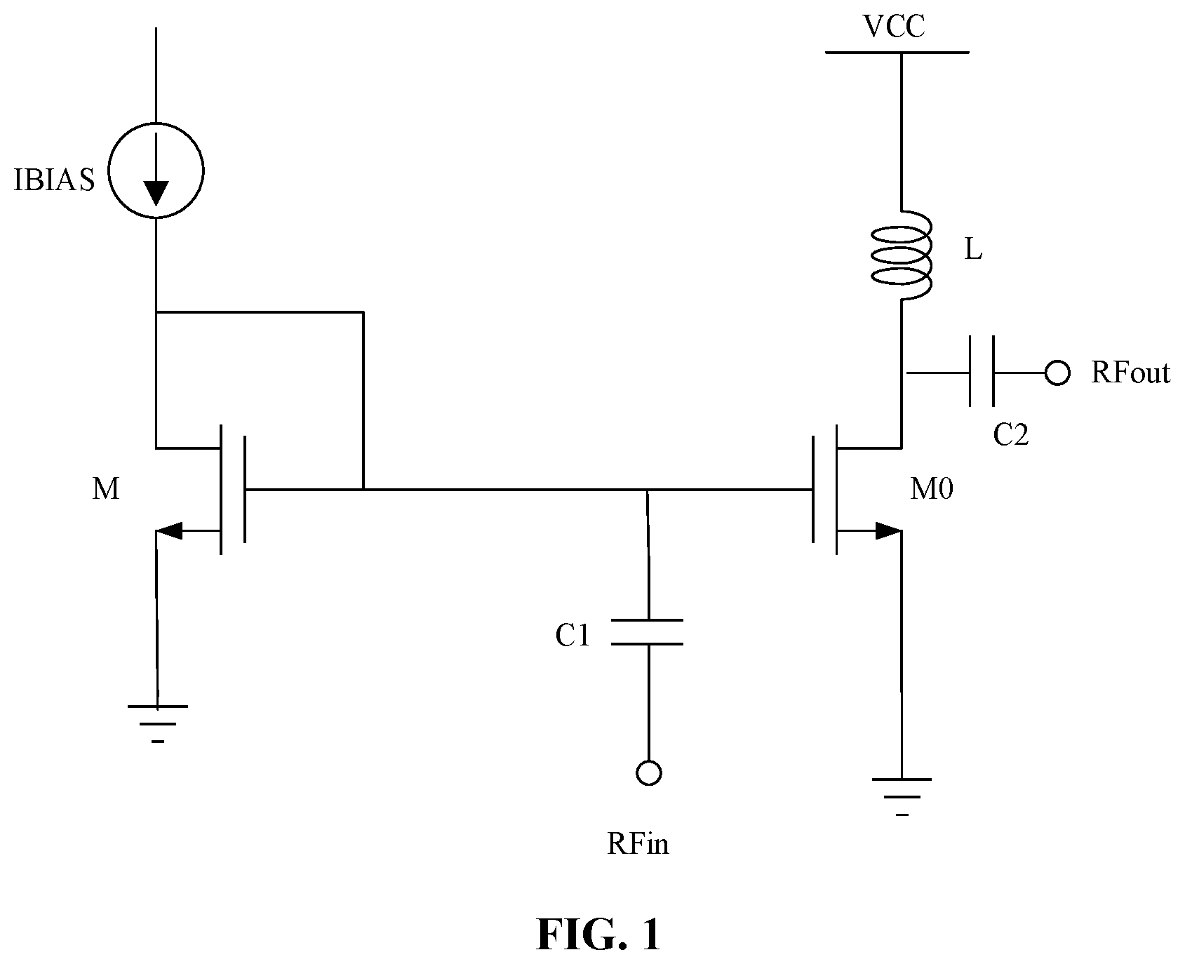
is a schematic structural diagram of the structure of a bias circuit of a power amplifier in some implementations;
is a schematic structural diagram of the first composition of a bias circuit of a power amplifier of an embodiment of this disclosure;
is a schematic structural diagram of the second structure of a bias circuit of a power amplifier of an embodiment of this disclosure;
is a schematic diagram of the relationship between the RF power and the bias voltage of an embodiment of this disclosure;
is a schematic diagram of the comparison result between the impedance of a bias circuit of an embodiment of this disclosure and the impedance of a bias circuit in some implementations;
is a schematic structural diagram of the third composition of a bias circuit of a power amplifier of an embodiment of this disclosure;
is a schematic structural diagram of a variable resistor of an embodiment of this disclosure;
is a schematic structural diagram of a variable capacitor of an embodiment of this disclosure; and
is a schematic diagram of the relationship between a RF power and gain amplitude and the relationship between a RF power and a bias voltage of an embodiment of this disclosure.
DETAILED DESCRIPTION
In order to better understand the characteristics and technical contents of embodiments in this disclosure, the implementation of the embodiments will be described in detail below with reference to the drawings, which are only for reference and illustration, and do not intend to limit the embodiments.
is a schematic diagram of a structure of a bias circuit in some implementations. As shown in , a bias circuit includes a transistor M and a current source IBIAS. The particularly connections are as follows. The drain of the transistor M is connected with the current source IBIAS, the source of the transistor M is grounded, and the drain of the transistor M is short-circuited with the gate. The gate of the M transistor is connected to the gate of the transistor M 0 of the power amplifier and is configured to provide a bias voltage for the gate of the M 0 transistor. The transistor M 0 is included in a signal amplification circuit for amplifying an input signal. The signal amplification circuit further includes a capacitor C 1 , a capacitor C 2 , a voltage source VCC and an inductor L. The specific connection mode of the signal amplification circuit is as follows. The gate of M 0 transistor is connected with one end of capacitor C 1 , and the other end of capacitor C 1 is used as the RF signal input end. The drain of the transistor M 0 is connected to the voltage source VCC through the inductor L and also connected to one end of the capacitor C 2 , the other end of the capacitor C 2 is used as the RF signal output end, and the source of the transistor M 0 is connected to a ground terminal. Based on the above bias circuit, since the transistor M is connected as a diode and the diode is a nonlinear component, the nonlinear effect causes the gate-source voltage of the transistor M to decrease with the increase of the power of the input RF signal, that is, the bias voltage provided to the transistor M 0 decreases, and then leads to the deterioration of the linearity of the transistor M 0 .
The embodiments of this disclosure provide a bias circuit of a power amplifier. is a schematic structure diagram of a first structure of a bias circuit of a power amplifier of an embodiment of this disclosure. As shown in , the bias circuit 11 includes a first part circuit 110 , a second part circuit 111 and a power supply 112 .
The power supply 112 is connected with a power supply terminal of the first part circuit 110 , and is configured to supply power to the first part circuit 110 .
The two ends of the first part circuit 110 are connected in parallel with the two ends of the second part circuit 111 , and one end of the parallel connected circuit is connected with the gate of the first transistor of the power amplifier 120 in the signal amplification circuit 12 ; the first part circuit 110 is configured to provide a first bias voltage to the gate of the first transistor; the second part circuit 111 is configured to provide a second bias voltage to the gate of the first transistor; the first bias voltage and the second bias voltage are superimposed to provide a stable bias voltage for the gate of the first transistor.
The impedance of the bias circuit is in a preset impedance range.
The first part circuit 110 is configured to provide a first bias voltage to the power amplifier 120 , and the second part circuit 111 is configured to provide a second bias voltage to the power amplifier 120 . When power of the RF signal input to the power amplifier 120 increases, the first bias voltage increases and the second bias voltage decreases, or alternatively, the first bias voltage decreases and the second bias voltage increases. The first bias voltage is adjusted by the second bias voltage, so as to provide a stable bias voltage to the power amplifier 120 , thereby ensuring the linearity performance of the power amplifier 120 .
It should be noted, the preset impedance range refers to the range that cannot cause the linearity of the power amplifier to deteriorate. The preset impedance range can be smaller than the impedance Z 1 of the bias circuit in , that is Z 1 =1/gm, where gm is the transconductance of the transistor M. When the impedance of the bias circuit is low, the linearity performance of the power amplifier can be guaranteed.
It should be noted, the first part circuit 110 and the second part circuit 111 also include other matching elements, such as one of or a combination of more of resistors, capacitors and transistors. The first part circuit 110 and the second part circuit 111 including one of or a combination of more of the elements provide a stable bias voltage to the power amplifier after superposition of the first bias voltage of the first part circuit 110 and the second bias voltage of the second part circuit 111 , and the impedance of the bias circuit 11 is within the preset impedance range, thus ensuring the linearity of the power amplifier 120 , and further effectively amplifying the input RF signal.
In addition, the signal amplification circuit 12 of includes a power amplifier 120 , which is configured to amplify the RF signal input from the signal input end and output the amplified RF signal from the signal output end.
Therefore, the first part circuit provides the first bias voltage to the power amplifier, and the second part circuit provides the second bias voltage to the power amplifier. The second bias voltage can adjust the first bias voltage to provide a stable bias voltage to the power amplifier. The impedance of the bias circuit is in the preset impedance range, thus ensuring the linearity performance of the power amplifier and reducing the memory effect of the power amplifier.
In view of the schematic structural diagram of the first composition of the bias circuit of the power amplifier in , this disclosure provides a specific circuit structural diagram, and is the schematic structural diagram of the second composition of a bias circuit of a power amplifier of an embodiment of this disclosure.
As shown in , the bias circuit 11 of the power amplifier includes the first part circuit 110 , the second part circuit 111 and the power supply 112 .
The power supply 112 includes a current source IBIAS, a first voltage source VCC 1 and a second voltage source VCC 2 . Herein, the power is supplied to IBIAS through VCC 2 .
The first part circuit 110 includes a second transistor M 2 , a third transistor M 3 , a first resistor R 1 and a first capacitor C 1 .
The specific connection mode is as follows: the drain of the transistor M 2 is connected with VCC 2 through IBIAS, and the drain and the gate of the transistor M 2 is connected with each other; the source of the transistor M 2 is connected to one end of the second part circuit 111 (that is, connected with the drain of a transistor M 4 ); the gate of the transistor M 2 is connected with the gate of the transistor M 3 through R 1 , and also connected with the ground terminal through C 1 ; the drain of the transistor M 3 is connected to VCC 1 , and the source of the transistor M 3 is connected to the other end of the second part circuit 111 (that is, connect to the drain of a transistor M 5 ) and the gate of a transistor M 1 .
The transistor M 2 and the transistor M 3 constitute a current mirror structure. R 1 and C 1 between the transistor M 2 and the transistor M 3 form a low-pass network circuit, to isolate the RF signal from being coupled into the bias current circuit, that is, to avoid affecting the transistor M 2 , thereby ensuring that the gate voltage of the transistor M 2 remains unchanged. Since the gate voltage of the transistor M 2 is equal to that of the transistor M 3 , the gate voltage of the transistor M 3 remains unchanged.
It should be noted, in the first part circuit, the gate and drain of the transistor M 2 are connected, that is, the transistor M 2 is a nonlinear component. Therefore, the first part circuit is a nonlinear circuit. Due to the nonlinearity of the transistor M 3 in the first part circuit and the RF signal on the gate-source voltage of the transistor M 3 , when power of the input RF signal is high, the gate-source voltage of the transistor M 3 decreases.
Herein, the gate-source voltage of the transistor M 3 is equal to the gate voltage of the transistor M 3 minus the source voltage. The gate-source voltage of the transistor M 3 decreases and the gate voltage of the transistor M 3 remains unchanged. Therefore, the source voltage of the transistor M 3 increases. That is, the first part circuit increases the voltage of V 2 node.
The second part circuit 111 includes a fourth transistor M 4 , a fifth transistor M 5 , a fourth resistor R 4 and a second capacitor C 2 .
The specific connection mode is as follows: the drain of the transistor M 4 is connected to one end of the first part circuit 110 (that is, to the source of the transistor M 2 ), and the source of the transistor M 4 is grounded; the gate of the transistor M 4 is connected with the gate of the transistor M 5 , and also connected with the ground terminal through C 2 ; the drain of the transistor M 5 is connected to the gate of the transistor M 5 through R 4 , and is also connected to the other end of the first part circuit 110 (that is, to the source of the transistor M 3 ). The source of the transistor M 5 is grounded.
It should be noted, the transistor M 4 and the transistor M 5 constitute a current mirror structure. R 4 and C 2 constitute a low-pass network circuit, to reduce the gate voltage of the transistor M 5 . Specifically, the drain of the transistor M 5 is connected to its gate through R 4 , that is, the transistor M 5 is connected as a diode and is a nonlinear component, so the nonlinear effect causes the gate-source voltage of the transistor M 5 to decrease with the increase of input RF signal power. Since the gate voltage of the transistor M 5 is equal to the drain voltage and the source voltage is equal to zero, the gate voltage of the transistor M 5 (that is, the voltage of V 1 node) decreases, that is, the second part circuit reduces the voltage of V 2 node.
Herein, the first part circuit increases the voltage of the V 2 node, and the second part circuit decreases the voltage of the V 2 node. When the voltage rise and fall of the two part circuits are designed to have the same extent of influence, by superimposing the two influences, V 2 node can present a stable DC bias voltage.
Based on the above description, is a schematic diagram of the relationship between RF power and bias voltage of an embodiment of this disclosure. As shown in , with the increase of RF power, the bias voltage of V 2 node increases when the transistor M 3 acts alone, while when the transistor M 5 acts alone, the bias voltage of V 2 node decreases; and when the transistors M 3 and M 5 act together, V 2 node has a stable DC bias voltage.
In addition, the transistor M 2 , the transistor M 3 , the transistor M 4 and the transistor M 5 constitute a closed loop and realize a low output impedance, and the impedance of V 2 node (that is, the impedance of bias circuit) is Z 2 =1/(gm3+gm5)(1+A), in which gm3 is the transconductance of the transistor M 3 , gm5 is the transconductance of the transistor M 5 , and A is the typical value of loop gain of about 100.
is a schematic diagram of the comparison result between an impedance of a bias circuit of an embodiment of this disclosure and that of a bias circuit in some implementations. As shown in , an impedance of a bias circuit in this disclosure is lower than that of the bias circuit in some implementations (that is, the impedance of ).
The bias circuit also includes a third resistor R 3 .
Herein, the source of the transistor M 3 is connected to the gate of the transistor M 1 through R 3 , and the drain of the transistor M 5 is connected to the gate of the transistor M 1 through R 3 .
It should be noted, R 3 is added to adjust the impedance frequency characteristics of the gate node of the transistor M 1 , so that the transistor M 1 has the best linearity. Herein, the value of R 3 is usually of more than ten and less than twenty ohms.
The signal amplifying circuit 12 also includes a third capacitor C 3 , a fourth capacitor C 4 , an inductor L and a third voltage source VCC 3 .
The specific connection mode is as follows: the gate of the transistor M 1 is connected with one end of C 3 , and the other end of C 3 is used as the signal input end; the drain of the transistor M 1 is connected with VCC 2 through L, and also connected with one end of C 4 , the other end of C 4 is used as the signal output end; the source of the transistor M 1 is grounded.
Herein, it should be noted, the transistors M 2 , M 3 , M 4 and M 5 mentioned above are transistors with the same structure. In addition, the transistor M 1 may or may not have the same structure as the transistors M 2 , M 3 , M 4 and M 5 .
Based on the schematic structural diagram of the first composition of the bias circuit of the power amplifier in , the disclosure also provides a specific circuit structural diagram, and is the schematic structural diagram of the third composition of a bias circuit of a power amplifier of an embodiment of the disclosure.
As shown in , the bias circuit 11 of the power amplifier includes the first part circuit 110 , the second part circuit 111 and the power supply 112 .
The power supply 112 includes a current source IBIAS, a first voltage source VCC 1 and a second voltage source VCC 2 . Herein, power is supplied to IBIAS through VCC 2 .
The first part circuit 110 includes a second transistor M 2 , a third transistor M 3 , a first resistor R 1 , a first capacitor C 1 and a second resistor R 2 . R 2 is a variable resistor.
The specific connection mode is as follows: the drain of the transistor M 2 is connected with VCC 2 through IBIAS, and the drain of the transistor M 2 is connected with its gate; the source of the transistor M 2 is connected to one end of the second part circuit 111 (that is, to the drain of the transistor M 4 ); the gate of the transistor M 2 is connected with the gate of the transistor M 3 through R 1 , and connected with the ground terminal through C 1 and R 2 in series. The drain of the transistor M 3 is connected to VCC 1 , and the source of the transistor M 3 is connected to the other end of the second circuit 111 (that is, to the drain of the transistor M 5 ) and the gate of the transistor M 1 .
is a schematic structural diagram of a variable resistor in the embodiments of this disclosure. As shown in , the variable resistor includes n resistors r and n switches S. The specific connection mode is as follows: r 1 and S 1 are connected in series, and then connected in parallel at both ends of r 2 and S 2 which are connected in series, and repeat, and then connected in parallel at both ends of rn and Sn which are connected in series.
It should be noted, the variable resistor R 2 connected in series with C 1 can control the effect of voltage increase of V 2 node on the transistor M 3 . For example, increasing R 2 can reduce the extent of increase of the bias voltage of V 2 node.
The second part circuit 111 includes a fourth transistor M 4 , a fifth transistor M 5 , a fourth resistor R 4 and a second capacitor C 2 . R 4 is a variable resistor and C 2 is a variable capacitor.
The specific connection mode is as follows: the drain of the transistor M 4 is connected to one end of the first part circuit 110 (that is, to the source of the transistor M 2 ), and the source of the transistor M 4 is grounded; the gate of the transistor M 4 is connected with the gate of the transistor M 5 , and also connected with the ground terminal through C 2 ; the drain of the transistor M 5 is connected to the gate of the transistor M 5 through R 4 , and is also connected to the other end of the first part circuit 110 (that is, to the source of The transistor M 3 ); and the source of the transistor M 5 is grounded.
is a schematic structural diagram of a variable capacitor of an embodiment of this disclosure. As shown in , the variable capacitor includes n capacitors c and n switches S. The specific connection mode is as follows: c 1 and S 1 are connected in series, and then are connected in parallel at both ends of c 2 and S 2 which are connected in series, and repeat, and at last connected in parallel at both ends of cn and Sn which are connected in series.
It should be noted, R 4 is a variable resistor and C 2 is a variable capacitor. By changing the values of R 4 and C 2 , the voltage reduction of V 2 node of the transistor M 5 can be controlled. For example, increasing R 4 and C 2 can reduce the bias voltage reduction effect of V 2 node.
Based on the above embodiments, by adjusting the values of R 2 , R 4 and C 2 , the bias voltage can be controllably increased or decreased with the increase of RF signal power. The optimal linear characteristics can be achieved by selecting appropriate bias voltage characteristics in the power amplifier.
The bias circuit further includes a third resistor R 3 .
Herein, the source of the transistor M 3 is connected to the gate of the transistor M 1 through R 3 , and the drain of the transistor M 5 is connected to the gate of the transistor M 1 through R 3 .
It should be noted, by increasing R 3 , the impedance-frequency characteristic of the gate node of the transistor M 1 is adjusted, so that the transistor M 1 has the best linearity. Herein, R 3 usually takes a value of more than ten and no more than twenty ohms.
The signal amplifying circuit 12 also includes a third capacitor C 3 , a fourth capacitor C 4 , an inductor L and a third voltage source VCC 3 .
The specific connection mode is as follows: the gate of the transistor M 1 is connected with one end of C 3 , and the other end of C 3 is used as a signal input end; the drain of the transistor M 1 is connected with VCC 2 through L, and also connected with one end of C 4 , the other end of C 4 is used as a signal output end; and the source of M 1 is grounded.
is a schematic diagram of the relationship between the RF power and gain amplitude and the relationship between RF power and bias voltage in an embodiment of this disclosure. As shown in , the abscissa is RF power, and the upper curves show the relationship between RF power and gain amplitude (that is, AMAM) of the power amplifier. From the AMAM curve, the 1 dB power compression point P 1 dB can be obtained, which can be used as a measurement index of the linearity of the power amplifier. The dotted line (i.e. normal bias) corresponds to the bias circuit having the fixed resistor and capacitor (i.e. R 4 and C 2 in the circuit of ), and the solid line (i.e. optimized bias) corresponds to the bias circuit having the variable resistors and variable capacitor (i.e. R 2 , R 4 and C 2 in the circuit of ). The lower curves show the relationship between RF power and bias voltage. The dotted line corresponds to the bias circuit having the fixed resistors and capacitors (i.e., normal bias), and the solid line corresponds to the bias circuit having the fixed of variable resistors and capacitors in (i.e. optimized bias).
As shown in , under the conventional bias, with the increase of RF power, the bias voltage remains unchanged and AMAM decreases. Under the optimized bias, by adjusting variable resistors and capacitors in the bias circuit, with the increase of RF power, the bias voltage increases, and AMAM also increases, thereby increasing the linearity of the power amplifier.
In addition, setting the variable resistors and capacitors is mainly to increase the flexibility of adjusting the linear power of the bias circuit. After the power amplifier is manufactured, the resistance and capacitance values with better linearity can be selected by digital control. For example, the power amplifier can work at different frequencies, and the resistance and capacitance with the optimal linearity are different at different frequencies. When using variable resistors and capacitors, the power amplifier can obtain the best linearity performance by setting different resistance and capacitance values at different frequencies.
The embodiments of this disclosure also provide a power amplification device, which comprises a power amplifier and any one of the bias circuit of the power amplifiers in the above embodiments.
The embodiments of the disclosure also disclose an electronic device, which comprises the power amplification device of the above embodiments of the disclosure.
The disclosure provides a bias circuit of a power amplifier, device and equipment. The circuit includes a first part circuit, a second part circuit and a power supply. The power supply is connected with a power supply end of the first part circuit. Two ends of the first part circuit are connected in parallel with two ends of the second part circuit, and after parallel connection one end of a parallel circuit is connected with a gate of the first transistor of the power amplifier in a signal amplification circuit. The first part circuit is configured to provide a first bias voltage, and the second part circuit is configured to provide a second bias voltage. The two bias voltages are superimposed to provide a stable bias voltage. An impedance of the bias circuit is in a preset impedance range. Therefore, the first circuit provides the first bias voltage for the power amplifier, and the second circuit provides the second bias voltage for the power amplifier. The second bias voltage can adjust the first bias voltage to provide the stable bias voltage for the power amplifier. In addition, the impedance of the bias circuit is in the preset range of the impedance, thus ensuring the linearity performance of the power amplifier and reducing the memory effect of the power amplifier.
Various modifications of, and equivalent acts corresponding to, the disclosed aspects of the example embodiments, in addition to those described above, can be made by a person of ordinary skill in the art, having the benefit of the present disclosure, without departing from the spirit and scope of the disclosure defined in the following claims, the scope of which is to be accorded the broadest interpretation so as to encompass such modifications and equivalent structures.
Figures (9)
Citations
This patent cites (8)
- US6486739
- US7259615
- US2001/0054933
- US2015/0061770
- US2016/0308500
- US2020/0244228
- US104426486
- US112994629