Method of Manufacturing Integrated Circuit Device
Abstract
In some embodiments, a method of manufacturing an integrated circuit device includes forming a feature structure on a substrate, forming a first hardmask configured to cover the feature structure, forming, on the first hardmask, a second hardmask comprising a plurality of first line portions extending lengthwise in a first horizontal direction and being apart from each other in a second horizontal direction perpendicular to the first horizontal direction, forming, on at least one of the first hardmask and the second hardmask, an etch mask pattern comprising a plurality of second line portions, forming, from the first hardmask, a first hardmask pattern comprising a plurality of third line portions, forming, from the second hardmask, a plurality of second hardmask patterns, and forming a feature pattern comprising a plurality of fourth line portions by etching the feature structure and using the plurality of second hardmask patterns and the first hardmask pattern.
Claims (20)
1. A method of manufacturing an integrated circuit device, comprising: forming a feature structure on a substrate; forming a first hardmask configured to cover the feature structure; forming, on the first hardmask, a second hardmask comprising a plurality of first line portions, the plurality of first line portions extending lengthwise in a first horizontal direction, each first line portion of the plurality of first line portions being apart from remaining first line portions of the plurality of first line portions in a second horizontal direction, the second horizontal direction being perpendicular to the first horizontal direction; forming, on the first hardmask and the second hardmask, an etch mask pattern comprising a plurality of second line portions, the plurality of second line portions extending lengthwise in the second horizontal direction, each second line portion of the plurality of second line portions being apart from remaining second line portions of the plurality of second line portions in the first horizontal direction; forming a first hardmask pattern from the first hardmask by etching the first hardmask and using the etch mask pattern as a first etch mask, the first hardmask pattern comprising a plurality of third line portions, each third line portion of the plurality of third line portions being parallel to remaining third line portions of the plurality of third line portions; forming a plurality of second hardmask patterns from the second hardmask by etching the second hardmask and using the etch mask pattern as a second etch mask; and forming a feature pattern by etching the feature structure and using the plurality of second hardmask patterns and the first hardmask pattern as a feature etch mask, the feature pattern comprising a plurality of fourth line portions, the plurality of fourth line portions extending lengthwise in the second horizontal direction, each fourth line portion of the plurality of fourth line portions being apart from remaining fourth line portions of the plurality of fourth line portions in the first horizontal direction.
11. A method of manufacturing an integrated circuit device, comprising: forming a plurality of fin-type active regions in a substrate; forming a plurality of dummy gate structures on the plurality of fin-type active regions; forming a cut space in at least one dummy gate structure selected from the plurality of dummy gate structures by partially etching the at least one dummy gate structure; and forming an isolation insulating film configured to fill the cut space, wherein the forming of the plurality of dummy gate structures comprises: forming a feature structure on the substrate in which the plurality of fin-type active regions are formed; forming a first hardmask configured to cover the feature structure; forming, on the first hardmask, a second hardmask comprising a plurality of first line portions, the plurality of first line portions extending lengthwise in a first horizontal direction, each first line portion of the plurality of first line portions being apart from remaining first line portions of the plurality of first line portions in a second horizontal direction, the second horizontal direction being perpendicular to the first horizontal direction; forming, on the first hardmask and the second hardmask, an etch mask pattern comprising a plurality of second line portions, the plurality of second line portions extending lengthwise in the second horizontal direction, each second line portion of the plurality of second line portions being apart from remaining second line portions of the plurality of second line portions in the first horizontal direction; forming a first hardmask pattern from the first hardmask by etching the first hardmask and using the etch mask pattern as a first etch mask, the first hardmask pattern comprising a plurality of third line portions, each third line portion of the plurality of third line portions being parallel to remaining third line portions of the plurality of third line portions; and forming a plurality of second hardmask patterns from the second hardmask by etching the second hardmask and using the etch mask pattern as a second etch mask; and wherein the forming of the plurality of dummy gate structures comprises forming the plurality of dummy gate structures to respectively comprise a plurality of fourth line portions by etching the feature structure by using the plurality of second hardmask patterns and the first hardmask pattern as a feature etch mask, the plurality of fourth line portions extending lengthwise in the second horizontal direction, and each fourth line portion of the plurality of fourth line portions being apart from remaining fourth line portions of the plurality of fourth line portions in the first horizontal direction.
19. A method of manufacturing an integrated circuit device, comprising: forming a plurality of fin-type active regions in a substrate to extend lengthwise in a first horizontal direction; forming a plurality of dummy gate structures on the plurality of fin-type active regions to extend lengthwise in a second horizontal direction, the second horizontal direction being perpendicular to the first horizontal direction; filling each space between the plurality of dummy gate structures with an insulating structure; forming, on the plurality of dummy gate structures and a plurality of insulating structures, a hardmask pattern having an opening that exposes at least one dummy gate structure selected from the plurality of dummy gate structures and a portion of the plurality of insulating structures; forming a cut space in the at least one dummy gate structure by selectively etching the at least one dummy gate structure from among the at least one dummy gate structure and the insulating structure; and forming an isolation insulating film configured to fill the cut space, wherein the forming of the plurality of dummy gate structures comprises: forming a feature structure on the substrate in which the plurality of fin-type active regions are formed; forming a first hardmask configured to cover the feature structure; forming, on the first hardmask, a second hardmask comprising a plurality of first line portions, the plurality of first line portions extending lengthwise in the first horizontal direction; forming, on the first hardmask and the second hardmask, an etch mask pattern comprising a plurality of second line portions, the plurality of second line portions extending lengthwise in the second horizontal direction; forming a first hardmask pattern comprising a line pattern from the first hardmask by etching the first hardmask and using the etch mask pattern as a first etch mask; forming a plurality of second hardmask patterns, respectively comprising a plurality of island patterns from the second hardmask, by etching the second hardmask and using the etch mask pattern as a second etch mask; and etching the feature structure by using the plurality of second hardmask patterns and the first hardmask pattern as a feature etch mask.
Show 17 dependent claims
2. The method of claim 1 , wherein the forming of the second hardmask comprises forming each first line portion of the plurality of first line portions to extend parallel to remaining first line portions of the plurality of first line portions in the first horizontal direction.
3. The method of claim 1 , wherein: the forming of the feature structure comprises forming the feature structure to comprise a polysilicon film and a dummy insulating capping layer covering the polysilicon film, and the forming of the feature pattern comprises forming each of the plurality of fourth line portions of the feature pattern to comprise a first portion of the polysilicon film and a second portion of the dummy insulating capping layer.
4. The method of claim 1 , wherein: the forming of the first hardmask comprises sequentially stacking a plurality of material layers in a vertical direction, each material layer of the plurality of material layers comprises a different material from remaining material layers of the plurality of material layers, the forming of the second hardmask comprises forming a layer comprising a distinct material that differs from a constituent material of an uppermost material layer from among the plurality of material layers of the first hardmask, and the uppermost material layer of the plurality of material layers of the first hardmask contacts the second hardmask.
5. The method of claim 1 , wherein the forming of the etch mask pattern comprises forming the etch mask pattern to cover a sidewall and an upper surface of each of first line portions disposed on the second hardmask.
6. The method of claim 1 , further comprising: after the forming of the feature pattern, forming an insulating structure configured to cover a sidewall of each of the plurality of fourth line portions of the feature pattern, a sidewall of each of the plurality of third line portions of the first hardmask pattern, and a sidewall of each of the plurality of second hardmask patterns, wherein the insulating structure fills each space between the plurality of fourth line portions, and an upper surface of the insulating structure and an upper surface of each of the plurality of second hardmask patterns horizontally extend at a same vertical level; forming, on the upper surface of each of the insulating structure and the plurality of second hardmask patterns, a third hardmask having an opening; forming a cut space in the feature pattern by etching the plurality of second hardmask patterns, the first hardmask pattern, and the feature pattern by using the third hardmask as a third etch mask; and forming an isolation insulating film configured to fill the cut space.
7. The method of claim 1 , wherein the etch mask pattern comprises a resist for extreme ultraviolet (EUV) light.
8. The method of claim 1 , wherein the forming of the etch mask pattern comprises forming the etch mask pattern to comprise only the plurality of second line portions.
9. The method of claim 1 , wherein the forming of the etch mask pattern comprises forming the etch mask pattern to comprise a connection portion extending lengthwise in the first horizontal direction and coupled to an end of each of two second line portions, the two second line portions having been selected from the plurality of second line portions and being adjacent to each other, such that the two second line portions are coupled to each other by the connection portion.
10. The method of claim 1 , wherein the forming of the etch mask pattern comprises forming the etch mask pattern to comprise a ring-shaped portion comprising two second line portions having been selected from the plurality of second line portions and being adjacent to each other.
12. The method of claim 11 , wherein each of the plurality of dummy gate structures comprises a polysilicon film and a dummy insulating capping layer covering the polysilicon film.
13. The method of claim 11 , wherein the forming of the etch mask pattern comprises forming the etch mask pattern to comprise a plurality of uneven portions at a lower surface thereof facing the substrate.
14. The method of claim 11 , further comprising: after the forming of the plurality of dummy gate structures, and before the forming of the cut space in the at least one dummy gate structure, forming an insulating structure configured to fill each space between the plurality of dummy gate structures; and forming, on an upper surface of each of the insulating structure and the plurality of second hardmask patterns, a third hardmask having an opening, wherein the forming of the cut space in the at least one dummy gate structure comprises selectively etching only the at least one dummy gate structure from among the at least one dummy gate structure and the insulating structure by using the third hardmask as a third etch mask.
15. The method of claim 11 , wherein: the etch mask pattern comprises: a bottom anti-reflective coating, which contacts the first hardmask and the second hardmask, and a photoresist pattern disposed on the bottom anti-reflective coating configured to cover the first hardmask and the second hardmask, and the photoresist pattern comprises a resist for extreme ultraviolet (EUV) light.
16. The method of claim 11 , wherein the forming of the etch mask pattern comprises forming the etch mask pattern to comprise only the plurality of second line portions.
17. The method of claim 11 , wherein: the forming of the etch mask pattern comprises coupling two second line portions selected from the plurality of second line portions, the two second line portions being adjacent to each other; and the forming of the plurality of dummy gate structures comprises forming each of the plurality of dummy gate structures to comprise a dummy connection portion coupled to ends of two fourth line portions adjacent to each other from among the plurality of fourth line portions such that the two fourth line portions are coupled to each other by the dummy connection portion.
18. The method of claim 17 , wherein the forming of the cut space in the at least one dummy gate structure comprises removing the dummy connection portion such that the two fourth line portions are separated from each other.
20. The method of claim 19 , wherein the forming of the etch mask pattern comprises forming the etch mask pattern such that two adjacent second line portions selected from the plurality of second line portions are coupled to each other.
Full Description
Show full text →
CROSS-REFERENCE TO RELATED APPLICATION
This application claims benefit of priority under 35 U.S.C. § 119 to Korean Patent Application No. 10-2022-0096754, filed on Aug. 3, 2022, in the Korean Intellectual Property Office, the disclosure of which is incorporated by reference herein in its entirety.
BACKGROUND
1. Field
The present disclosure relates generally to a method of manufacturing an integrated circuit device, and more particularly, to a method of manufacturing an integrated circuit device, the method including a process of forming a line pattern.
2. Description of Related Art
Due to the development of electronics technology, semiconductor devices have been rapidly down-scaled. Accordingly, when relatively long and narrow line patterns are formed in device regions having relatively small areas, process defects, such as the unintended leaning or collapse of the line patterns, may be generated. Therefore, it may be required to develop a technique for optimizing the performance of integrated circuit devices and improving the reliability thereof, by stably forming long and narrow line patterns.
SUMMARY
The present disclosure provides a method of manufacturing an integrated circuit device, the method allowing the integrated circuit device having optimized performance and improved reliability to be manufactured by stably forming long and narrow line patterns during a process of manufacturing the integrated circuit device having a device region that is reduced in area due to down-scaling.
According to an aspect of the present disclosure, a method of manufacturing an integrated circuit device is provided. The method includes forming a feature structure on a substrate. The method further includes forming a first hardmask configured to cover the feature structure. The method further includes forming, on the first hardmask, a second hardmask including a plurality of first line portions. The plurality of first line portions extends lengthwise in a first horizontal direction. Each first line portion of the plurality of first line portions is apart from remaining first line portions of the plurality of first line portions in a second horizontal direction. The second horizontal direction is perpendicular to the first horizontal direction. The method further includes forming, on at least one of the first hardmask and the second hardmask, an etch mask pattern that includes a plurality of second line portions. The plurality of second line portions extends lengthwise in the second horizontal direction. Each second line portion of the plurality of second line portions is apart from remaining second line portions of the plurality of second line portions in the first horizontal direction. The method further includes forming a first hardmask pattern from the first hardmask by etching the first hardmask and using the etch mask pattern as a first etch mask. The first hardmask pattern includes a plurality of third line portions. Each third line portion of the plurality of third line portions is parallel to remaining third line portions of the plurality of third line portions. The method further includes forming a plurality of second hardmask patterns from the second hardmask by etching the second hardmask and using the etch mask pattern as a second etch mask. The method further includes forming a feature pattern by etching the feature structure and using the plurality of second hardmask patterns and the first hardmask pattern as a feature etch mask. The feature pattern includes a plurality of fourth line portions. The plurality of fourth line portions extends lengthwise in the second horizontal direction. Each fourth line portion of the plurality of fourth line portions is apart from remaining fourth line portions of the plurality of fourth line portions in the first horizontal direction.
According to an aspect of the present disclosure, another method of manufacturing an integrated circuit device is provided. The method includes forming a plurality of fin-type active regions in a substrate. The method further includes forming a plurality of dummy gate structures on the plurality of fin-type active regions. The method further includes forming a cut space in at least one dummy gate structure selected from the plurality of dummy gate structures by partially etching the at least one dummy gate structure. The method further includes forming an isolation insulating film configured to fill the cut space. The forming of the plurality of dummy gate structures includes forming a feature structure on the substrate in which the plurality of fin-type active regions are formed. The forming of the plurality of dummy gate structures further includes forming a first hardmask configured to cover the feature structure. The forming of the plurality of dummy gate structures further includes forming, on the first hardmask, a second hardmask including a plurality of first line portions. The plurality of first line portions extends lengthwise in a first horizontal direction. Each first line portion of the plurality of first line portions is apart from remaining first line portions of the plurality of first line portions in a second horizontal direction. The second horizontal direction is perpendicular to the first horizontal direction. The forming of the plurality of dummy gate structures further includes forming, on at least one of the first hardmask and the second hardmask, an etch mask pattern including a plurality of second line portions. The plurality of second line portions extends lengthwise in the second horizontal direction. Each second line portion of the plurality of second line portions is apart from remaining second line portions of the plurality of second line portions in the first horizontal direction. The forming of the plurality of dummy gate structures further includes forming a first hardmask pattern from the first hardmask by etching the first hardmask and using the etch mask pattern as a first etch mask. The first hardmask pattern includes a plurality of third line portions. Each third line portion of the plurality of third line portions is parallel to remaining third line portions of the plurality of third line portions. The forming of the plurality of dummy gate structures further includes forming a plurality of second hardmask patterns from the second hardmask by etching the second hardmask and using the etch mask pattern as a second etch mask. The forming of the plurality of dummy gate structures includes forming the plurality of dummy gate structures to respectively include a plurality of fourth line portions by etching the feature structure by using the plurality of second hardmask patterns and the first hardmask pattern as a feature etch mask. The plurality of fourth line portions extends lengthwise in the second horizontal direction. Each fourth line portion of the plurality of fourth line portions is apart from remaining fourth line portions of the plurality of fourth line portions in the first horizontal direction.
According to an aspect of the present disclosure, another method of manufacturing an integrated circuit device is provided. The method includes forming a plurality of fin-type active regions in a substrate to extend lengthwise in a first horizontal direction. The method further includes forming a plurality of dummy gate structures on the plurality of fin-type active regions to extend lengthwise in a second horizontal direction. The second horizontal direction is perpendicular to the first horizontal direction. The method further includes filling each space between the plurality of dummy gate structures with an insulating structure. The method further includes forming, on the plurality of dummy gate structures and a plurality of insulating structures, a hardmask pattern having an opening that exposes at least one dummy gate structure selected from the plurality of dummy gate structures and a portion of the plurality of insulating structures. The method further includes forming a cut space in the at least one dummy gate structure by selectively etching the at least one dummy gate structure from among the at least one dummy gate structure and the insulating structure. The method further includes forming an isolation insulating film configured to fill the cut space. The forming of the plurality of dummy gate structures includes forming a feature structure on the substrate in which the plurality of fin-type active regions are formed. The forming of the plurality of dummy gate structures further includes forming a first hardmask configured to cover the feature structure. The forming of the plurality of dummy gate structures further includes forming, on the first hardmask, a second hardmask including a plurality of first line portions. The plurality of first line portions extends lengthwise in the first horizontal direction. The forming of the plurality of dummy gate structures further includes forming, on the first hardmask and the second hardmask, an etch mask pattern including a plurality of second line portions. The plurality of second line portions extends lengthwise in the second horizontal direction. The forming of the plurality of dummy gate structures further includes forming a first hardmask pattern including a line pattern from the first hardmask by etching the first hardmask and using the etch mask pattern as a first etch mask. The forming of the plurality of dummy gate structures further includes forming a plurality of second hardmask patterns, respectively including a plurality of island patterns from the second hardmask, by etching the second hardmask and using the etch mask pattern as a second etch mask. The forming of the plurality of dummy gate structures further includes etching the feature structure by using the plurality of second hardmask patterns and the first hardmask pattern as a feature etch mask.
BRIEF DESCRIPTION OF THE DRAWINGS
The above and other aspects, features, and advantages of certain embodiments of the present disclosure will be more apparent from the following description taken in conjunction with the accompanying drawings, in which:
A to 9 D are diagrams illustrating a method of manufacturing an integrated circuit device, according to some embodiments, and in particular, A, 2 A, 3 A, 4 A, 5 A, 6 A, 7 A, 8 A, and 9 A are plan views respectively illustrating a sequence of processes of the method of manufacturing an integrated circuit device, B, 2 B, 3 B, 4 B, 5 B, 6 B, 7 B, 8 B, and 9 B are cross-sectional views taken along lines Y 1 -Y 1 ′ of A, 2 A, 3 A, 4 A, 5 A, 6 A, 7 A, 8 A, and 9 A , respectively, C, 2 C, 3 C, 4 C, 5 C, 6 C, 7 C, 8 C, and 9 C are cross-sectional views taken along lines X 1 -X 1 ′ of A, 2 A, 3 A, 4 A, 5 A, 6 A, 7 A, 8 A, and 9 A , respectively, and D, 2 D, 3 D, 4 D, 5 D, 6 D, 7 D, 8 D, and 9 D are cross-sectional views taken along lines X 2 -X 2 ′ of A, 2 A, 3 A, 4 A, 5 A, 6 A, 7 A, 8 A, and 9 A , respectively;
to 12 are plan views respectively illustrating various planar shapes of an etch mask pattern that may be formed by a method of manufacturing an integrated circuit device, according to some embodiments; and
to 17 are plan views respectively illustrating various planar shapes of a gate line structure that may be formed by a method of manufacturing an integrated circuit device, according to some embodiments.
DETAILED DESCRIPTION
The following description with reference to the accompanying drawings is provided to assist in a comprehensive understanding of embodiments of the present disclosure defined by the claims and their equivalents. Various specific details are included to assist in understanding, but these details are considered to be exemplary only. Therefore, those of ordinary skill in the art will recognize that various changes and modifications of the embodiments described herein can be made without departing from the scope and spirit of the disclosure. In addition, descriptions of well-known functions and structures are omitted for clarity and conciseness.
With regard to the description of the drawings, similar reference numerals may be used to refer to similar or related elements. It is to be understood that a singular form of a noun corresponding to an item may include one or more of the things, unless the relevant context clearly indicates otherwise. As used herein, each of such phrases as “A or B,” “at least one of A and B,” “at least one of A or B,” “A, B, or C,” “at least one of A, B, and C,” and “at least one of A, B, or C,” may include any one of, or all possible combinations of the items enumerated together in a corresponding one of the phrases. As used herein, such terms as “1st” and “2nd,” or “first” and “second” may be used to simply distinguish a corresponding component from another, and does not limit the components in other aspect (e.g., importance or order). It is to be understood that if an element (e.g., a first element) is referred to, with or without the term “operatively” or “communicatively”, as “coupled with,” “coupled to,” “connected with,” or “connected to” another element (e.g., a second element), it means that the element may be coupled with the other element directly (e.g., wired), wirelessly, or via a third element.
It will be understood that when an element or layer is referred to as being “over,” “above,” “on,” “below,” “under,” “beneath,” “connected to” or “coupled to” another element or layer, it can be directly over, above, on, below, under, beneath, connected or coupled to the other element or layer or intervening elements or layers may be present. In contrast, when an element is referred to as being “directly over,” “directly above,” “directly on,” “directly below,” “directly under,” “directly beneath,” “directly connected to” or “directly coupled to” another element or layer, there are no intervening elements or layers present.
The terms “upper,” “middle”, “lower”, etc. may be replaced with terms, such as “first,” “second,” third” to be used to describe relative positions of elements. The terms “first,” “second,” third” may be used to described various elements but the elements are not limited by the terms and a “first element” may be referred to as a “second element”. Alternatively or additionally, the terms “first”, “second”, “third”, etc. may be used to distinguish components from each other and do not limit the present disclosure. For example, the terms “first”, “second”, “third”, etc. may not necessarily involve an order or a numerical meaning of any form.
Reference throughout the present disclosure to “one embodiment,” “an embodiment,” “an example embodiment,” or similar language may indicate that a particular feature, structure, or characteristic described in connection with the indicated embodiment is included in at least one embodiment of the present solution. Thus, the phrases “in one embodiment”, “in an embodiment,” “in an example embodiment,” and similar language throughout this disclosure may, but do not necessarily, all refer to the same embodiment.
A to 9 D are diagrams illustrating a method of manufacturing an integrated circuit device 100 (see A to 9 D ), according to some embodiments. More specifically, A, 2 A, 3 A, 4 A, 5 A, 6 A, 7 A, 8 A, and 9 A are plan views respectively illustrating a sequence of processes of the method of manufacturing the integrated circuit device 100 . B, 2 B, 3 B, 4 B, 5 B, 6 B, 7 B, 8 B, and 9 B are cross-sectional views taken along lines Y 1 -Y 1 ′ of A, 2 A, 3 A, 4 A, 5 A, 6 A, 7 A, 8 A, and 9 A , respectively. C, 2 C, 3 C, 4 C, 5 C, 6 C, 7 C, 8 C, and 9 C are cross-sectional views taken along lines X 1 -X 1 ′ of A, 2 A, 3 A, 4 A, 5 A, 6 A, 7 A, 8 A, and 9 A , respectively. D, 2 D, 3 D, 4 D, 5 D, 6 D , 7 D, 8 D, and 9 D are cross-sectional views taken along lines X 2 -X 2 ′ of A, 2 A, 3 A, 4 A, 5 A, 6 A, 7 A, 8 A, and 9 A , respectively.
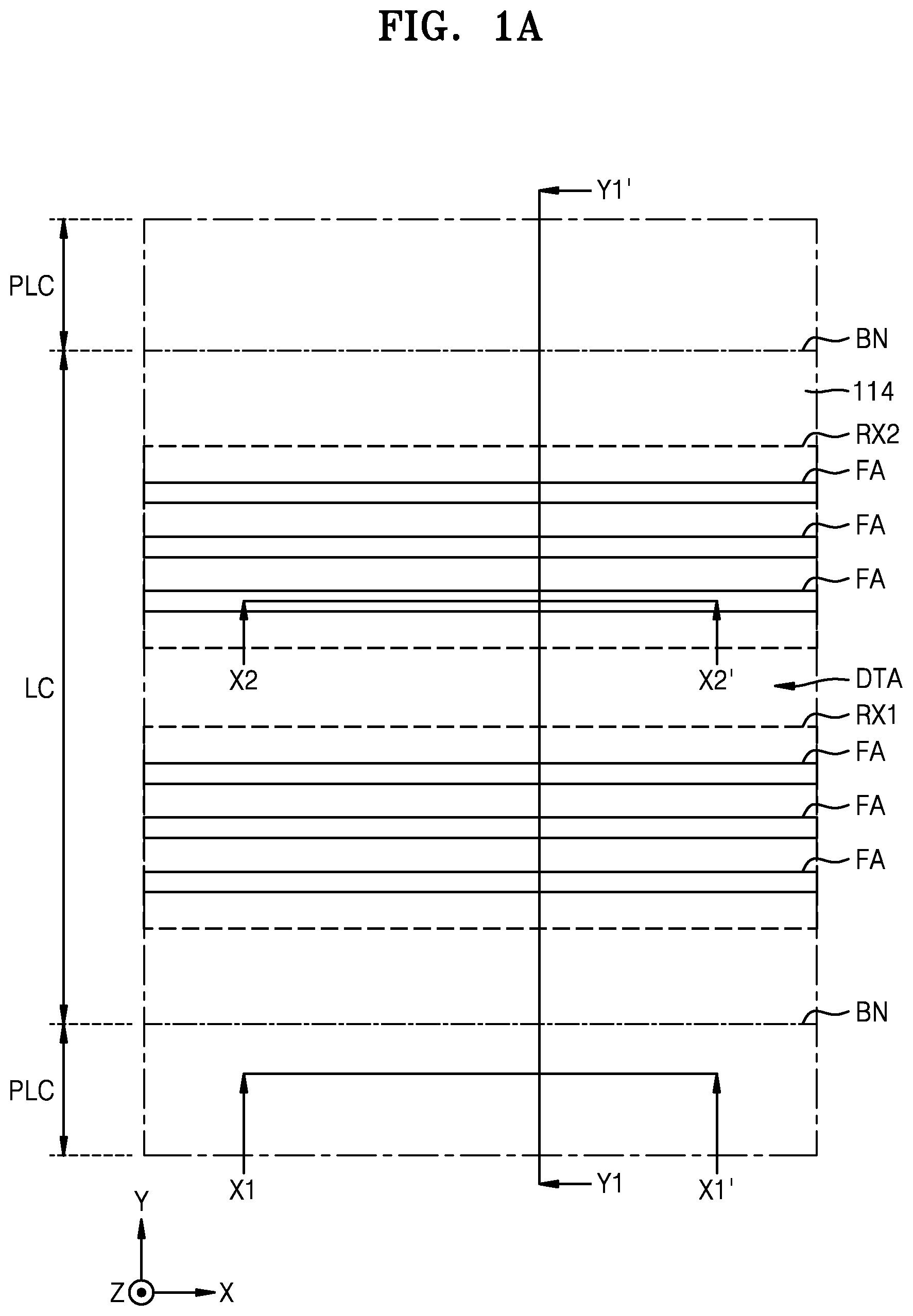
Referring to A to 1 D , a substrate 110 may be prepared that may include a cell area LC and a cell peripheral area PLC around the cell area LC. The cell area LC may be defined by a cell boundary BN.
The substrate 110 may include a semiconductor, such as, but not limited to, silicon (Si) or germanium (Ge), and/or a compound semiconductor, such as, but not limited to, silicon—germanium (SiGe), silicon carbide (SiC), gallium arsenide (GaAs), indium arsenide (InAs), or indium phosphide (InP). Alternatively or additionally, the substrate 110 may include a conductive region, for example, an impurity-doped well and/or an impurity-doped structure. In some embodiments, the cell area LC may include a first device region RX 1 , a second device region RX 2 , and an inter-device isolation region DTA therebetween.
The substrate 110 in the first device region RX 1 and the second device region RX 2 may be partially etched, thereby forming a plurality of fin-type active regions FA, which protrude in a vertical direction (e.g., Z direction) from a main surface 110 M of the substrate 110 and extend parallel to each other in a first horizontal direction (e.g., X direction).
In some embodiments, a device isolation film 112 may be formed to cover both sidewalls of a lower portion of each of the plurality of fin-type active regions FA. A deep trench DT may be formed to define the first device region RX 1 and the second device region RX 2 by etching a portion of the device isolation film 112 and a portion of the substrate 110 . The deep trench DT may be filled with an inter-device isolation insulating film 114 . In the first device region RX 1 and the second device region RX 2 , the plurality of fin-type active regions FA may protrude upward from an upper surface of the device isolation film 112 .
Referring to A to 2 D , a feature structure D 10 may be formed to cover the plurality of fin-type active regions FA, the device isolation film 112 , and the inter-device isolation insulating film 114 .
The feature structure D 10 may include a dummy gate insulating film D 12 , a dummy gate line D 14 , and a dummy insulating capping layer D 16 , which may be sequentially formed on the plurality of fin-type active regions FA in the stated order. That is, the dummy gate line D 14 may be formed to cover the dummy gate insulating film D 12 , the device isolation film 112 , and the inter-device isolation insulating film 114 . Alternatively or additionally, the dummy insulating capping layer D 16 may be formed to cover the dummy gate line D 14 . The feature structure D 10 may have a planarized upper surface. In some embodiments, the dummy gate insulating film D 12 may include a silicon oxide (SiO) film. Alternatively or additionally, the dummy gate line D 14 may include a polysilicon film, and the dummy insulating capping layer D 16 may include a silicon nitride (SiN) film.
Referring to A to 3 D , a first hardmask HM 1 may be formed to cover the feature structure D 10 , and/or a second hardmask HM 2 may be formed on the first hardmask HM 1 .
In some embodiments, the first hardmask HM 1 may include a plurality of material layers, which respectively include different materials from each other and are sequentially stacked in the vertical direction. For example, the first hardmask HM 1 may have, but is not limited to, a structure in which a silicon oxide film, a silicon nitride film, and a tetraethyl orthosilicate (TEOS) film that may be sequentially stacked in the stated order by an atomic layer deposition (ALD) process.
The second hardmask HM 2 may include a plurality of first line portions L 1 , which extend lengthwise in the first horizontal direction (e.g., X direction) and are apart from each other in a second horizontal direction (e.g., Y direction) that is perpendicular to the first horizontal direction (e.g., X direction). The plurality of first line portions L 1 of the second hardmask HM 2 may extend parallel to each other in the first horizontal direction (e.g., X direction).
The second hardmask HM 2 may include a single layer including a different material from a constituent material of an uppermost material layer contacting the second hardmask HM 2 from among the plurality of material layers that constitute the first hardmask HM 1 . For example, the uppermost material layer of the first hardmask HM 1 may include a silicon oxide film, and the second hardmask HM 2 may include a silicon nitride film, but the present disclosure is not limited thereto.
Referring to A to 4 D , an etch mask pattern MPR, which may include a plurality of second line portions L 2 may be formed on the first hardmask HM 1 and the second hardmask HM 2 .
The plurality of second line portions L 2 of the etch mask pattern MPR may extend lengthwise and parallel to each other in the second horizontal direction (e.g., Y direction) while being apart from each other in the first horizontal direction (e.g., X direction), on the first hardmask HM 1 and the second hardmask HM 2 .
The etch mask pattern MPR may include a bottom anti-reflective coating (BARC) 118 , which may contact each of the first hardmask HM 1 and the second hardmask HM 2 , and a photoresist pattern PR, which may be arranged on the BARC 118 to cover each of the first hardmask HM 1 and the second hardmask HM 2 . Each of the plurality of second line portions L 2 may include a portion of the photoresist pattern PR and a portion of the BARC 118 .
In some embodiments, the photoresist pattern PR may include a resist for extreme ultraviolet (EUV) light (e.g., light having a wavelength of approximately 13.5 nanometers (nm)). In some embodiments, the BARC 118 may include an organic compound, an inorganic compound, or a combination thereof. For example, the BARC 118 may include, but not be limited to, silicon nitride, silicon oxynitride, amorphous silicon, titanium, titanium dioxide, titanium nitride, chromium oxide, carbon, an organic anti-reflective coating (ARC) material, or a combination thereof. The organic ARC material may include, but not be limited to, an acrylic resin having a hydroxyl group (e.g., a crosslinking group and an optical absorption group in the same molecule), or a novolac resin having a hydroxyl group.
As shown in B , each of the plurality of second line portions L 2 of the etch mask pattern MPR may be formed to cover a sidewall and an upper surface of each of the plurality of first line portions L 1 of the second hardmask HM 2 . Accordingly, the etch mask pattern MPR may include a plurality of uneven portions at a lower surface thereof facing the substrate 110 . For example, the plurality of uneven portions may have uneven shapes corresponding to the plurality of first line portions L 1 of the second hardmask HM 2 , respectively.
In some embodiments, the plurality of second line portions L 2 of the etch mask pattern MPR may be supported by the second hardmask HM 2 arranged thereunder. Therefore, process defects (e.g., the unintended leaning or collapse of the plurality of second line portions L 2 of the etch mask pattern MPR) may be prevented, and the plurality of second line portions L 2 of the etch mask pattern MPR may maintain stable shapes thereof during a subsequent process using the etch mask pattern MPR after the etch mask pattern MPR is formed.
to 12 are plan views respectively illustrating various planar shapes of the etch mask pattern MPR shown in A to 4 D .
In some embodiments, referring to A to 4 D , the etch mask pattern MPR may include an etch mask pattern MPR 1 including only the plurality of second line portions L 2 , as shown in . That is, the plurality of second line portions L 2 may be arranged throughout the cell area LC and the cell peripheral area PLC.
Continuing to refer to A to 4 D , in some embodiments, the etch mask pattern MPR may include an etch mask pattern MPR 2 including the plurality of second line portions L 2 and a plurality of connection portions LK 2 . The plurality of connection portions LK 2 may be connected between two second line portions L 2 that are selected from the plurality of second line portions L 2 and may be adjacent to each other, as shown in .
In the etch mask pattern MPR, the plurality of second line portions L 2 may be arranged throughout the cell area LC and the cell peripheral area PLC, and the plurality of connection portions LK 2 may be arranged in the cell peripheral area PLC. Each of the plurality of connection portions LK 2 may be connected to an end of each of the two second line portions L 2 to connect the two second line portions L 2 to each other. The two second line portions L 2 may be selected from the plurality of second line portions L 2 and may be adjacent to each other. The etch mask pattern MPR 2 may include a portion having a planar shape of a ring, which may be formed by the two second line portions L 2 and two connection portions LK 2 connecting the two second line portions L 2 to each other.
In some embodiments, the etch mask pattern MPR, as shown in A to 4 D , may include an etch mask pattern MPR 3 including the plurality of second line portions L 2 and a plurality of connection portions LK 3 . The plurality of connection portions LK 3 may be connected between two second line portions L 2 that are selected from the plurality of second line portions L 2 and may be adjacent to each other, as shown in .
In the etch mask pattern MPR 3 , the plurality of second line portions L 2 may be arranged throughout the cell area LC and the cell peripheral area PLC, and the plurality of connection portions LK 3 may be arranged in the cell peripheral area PLC. Similar to the plurality of connection portions LK 2 shown in , each of the plurality of connection portions LK 3 may be connected to an end of each of the two second line portions L 2 to connect the two second line portions L 2 to each other. The two second line portions L 2 may be selected from the plurality of second line portions L 2 and may be adjacent to each other. In some embodiments, the etch mask pattern MPR 3 may include a portion having a planar structure in which every two adjacent second line portions L 2 are connected to each other by each of the plurality of connection portions LK 3 to form a repetitive S-shape.
Referring to A to 5 D , the second hardmask HM 2 and the first hardmask HM 1 may be etched by using the etch mask pattern MPR as an etch mask. As a result, a first hardmask pattern HM 1 P including a plurality of third line portions L 3 , which are parallel to each other, may be formed from the first hardmask HM 1 , and a plurality of second hardmask patterns HM 2 P, which respectively include a plurality of island patterns on the first hardmask pattern HM 1 P, may be formed from the second hardmask HM 2 .
The feature structure D 10 may be etched by using the plurality of second hardmask patterns HM 2 P and the first hardmask pattern HM 1 P as an etch mask, thereby forming a plurality of dummy gate structures DGS. The plurality of dummy gate structures DGS may respectively include a plurality of fourth line portions L 4 extending lengthwise in the second horizontal direction (e.g., Y direction). The plurality of fourth line portions L 4 , which are respectively included in the plurality of dummy gate structures DGS, may be apart from each other in the first horizontal direction (e.g., X direction) and extend parallel to each other in the second horizontal direction (e.g., Y direction). Herein, the plurality of dummy gate structures DGS may be referred to as a feature pattern.
Each of the plurality of fourth line portions L 4 , which are respectively included in the plurality of dummy gate structures DGS, may include a portion of the dummy gate insulating film D 12 , a portion of the dummy gate line D 14 , and a portion of the dummy insulating capping layer D 16 .
The plurality of dummy gate structures DGS may have various planar shapes, similar to the description made regarding various planar shapes of the etch mask pattern MPR as shown in A to 4 D with reference to to 12 . In some embodiments, the plurality of dummy gate structures DGS may respectively include only the plurality of fourth line portions L 4 , similar to the etch mask pattern MPR 1 shown in . In some embodiments, each of the plurality of dummy gate structures DGS may include a dummy connection portion connected to ends of two fourth line portions L 4 adjacent to each other from among the plurality of fourth line portions L 4 such that the two adjacent fourth line portions L 4 are connected to each other by the dummy connection portion, similar to the etch mask pattern MPR 2 shown in . In some embodiments, the dummy connection portion may have a planar shape that is the same as or similar to that of the connection portion LK 2 shown in .
Referring to A to 6 D , in a resulting product of A to 5 D , a plurality of insulating spacers 122 may be formed to cover both sidewalls of each of the plurality of dummy gate structures DGS, and portions of the plurality of fin-type active regions FA, which are exposed on both sides of each of the plurality of dummy gate structures DGS. In some embodiments, the plurality of fin-type active regions FA may be etched, thereby forming a plurality of recess regions RR in an upper surface of each of the plurality of fin-type active regions FA. A plurality of source/drain regions SD may be formed to respectively fill the plurality of recess regions RR. Additionally or alternatively, an inter-gate dielectric 128 may be formed to fill each space between the plurality of dummy gate structures DGS. The inter-gate dielectric 128 may be formed to cover the plurality of insulating spacers 122 , the device isolation film 112 , the inter-device isolation insulating film 114 , and the plurality of source/drain regions SD.
An insulating spacer 122 and the inter-gate dielectric 128 may constitute an insulating structure 120 . In the insulating structure 120 , the inter-gate dielectric 128 may fill each space, which may be defined by the insulating spacer 122 , between the plurality of dummy gate structures DGS.
In some embodiments, each of the plurality of insulating spacers 122 may include a portion extending in a line shape in the second horizontal direction (e.g., Y direction). The insulating spacer 122 may include, but not be limited to, a silicon nitride (SiN) film, a silicon oxycarbonitride (SiOCN) film, silicon carbonitride (SiCN) film, or a combination thereof. The inter-gate dielectric 128 may include, but is not limited to, a silicon oxide (SiO) film. In some embodiments, before the inter-gate dielectric 128 is formed, the method of manufacturing the integrated circuit device 100 may further include a process of forming an insulating liner (not shown) to cover the plurality of insulating spacers 122 and the plurality of source/drain regions SD. The insulating liner may include silicon nitride (SiN), silicon carbonitride (SiCN), silicon boron nitride (SiBN), silicon oxynitride (SiON), silicon oxycarbonitride (SiOCN), silicon boron carbonitride (SiBCN), silicon oxycarbide (SiOC), silicon oxide (SiO), or a combination thereof. As used herein, each of the terms “SiN”, “SiCN”, “SiBN”, “SiON”, “SiOCN”, “SiBCN”, “SiOC”, and “SiO” may refer to a material made of elements included in each of the terms and is not a chemical formula representing a stoichiometric relationship.
The insulating structure 120 may cover a sidewall of each of the plurality of fourth line portions L 4 of the plurality of dummy gate structures DGS, a sidewall of each of the plurality of third line portions L 3 of the first hardmask pattern HM 1 P, and a sidewall of each of the plurality of second hardmask patterns HM 2 P. An upper surface of the insulating structure 120 and an upper surface of each of the plurality of second hardmask patterns HM 2 P may extend in a horizontal direction at the same vertical level or respectively at similar vertical levels. As used herein, the term “vertical level” may refer to a distance in the vertical direction (e.g., Z direction) from the main surface 110 M of the substrate 110 .
Referring to A to 7 D , in a resulting product of A to 6 D , a third hardmask HM 3 may be formed on the upper surface of each of the insulating structure 120 and the plurality of second hardmask patterns HM 2 P. The third hardmask HM 3 may include a plurality of openings H 3 , which expose a portion of the insulating structure 120 and portions of the plurality of second hardmask patterns HM 2 P, in the cell peripheral area PLC.
In some embodiments, portions of the plurality of second hardmask patterns HM 2 P, a portion of the first hardmask pattern HM 1 P, and portions of the plurality of dummy gate structures DGS may be etched by using the third hardmask HM 3 as an etch mask, thereby forming a plurality of cut spaces GC respectively in the plurality of dummy gate structures DGS.
The third hardmask HM 3 may include a plurality of mask layers including different materials from each other. The plurality of mask layers may include a first mask layer 132 , a second mask layer 134 , and a third mask layer 136 , which may be sequentially stacked in the stated order on the upper surface of each of the insulating structure 120 and the plurality of second hardmask patterns HM 2 P. In some embodiments, the first mask layer 132 may include a silicon oxide film formed by an ALD process, the second mask layer 134 may include a silicon nitride film, and the third mask layer 136 may include a TEOS film, but the present disclosure is not limited thereto.
In related techniques, to form the plurality of openings H 3 in the third hardmask HM 3 , when the third mask layer 136 , the second mask layer 134 , and the first mask layer 132 are etched in the stated order from top to bottom, the insulating structure 120 exposed by the plurality of openings H 3 may be partially recessed due to unintended over-etching. However, according to the method of manufacturing the integrated circuit device 100 provided by the present disclosure, when the third mask layer 136 , the second mask layer 134 , and the first mask layer 132 are etched in the stated order from top to bottom to form the plurality of openings H 3 in the third hardmask HM 3 , the plurality of second hardmask patterns HM 2 P under the third hardmask HM 3 may improve an etch mask function of the third hardmask HM 3 . Accordingly, the insulating structure 120 exposed by the plurality of openings H 3 may be prevented from being partially recessed due to unintended over-etching. Therefore, unintended consumption of the insulating structure 120 may be suppressed while the plurality of openings H 3 are formed in the third hardmask HM 3 , and thus, the reliability of the integrated circuit device 100 may be prevented from being deteriorated due to the damage to the insulating structure 120 .
Alternatively or additionally, when forming the plurality of cut spaces GC, and the plurality of dummy gate structures DGS exposed by the plurality of openings H 3 are etched, the insulating structure 120 , together with the plurality of dummy gate structures DGS, may also be exposed by the plurality of cut spaces GC. Here, the plurality of second hardmask patterns HM 2 P under the third hardmask HM 3 may improve the etch mask function of the third hardmask HM 3 , and thus, a selective etching process, in which only the plurality of dummy gate structures DGS from among the plurality of dummy gate structures DGS and the insulating structure 120 are selectively etched, may have an improved efficiency.
Referring to A to 8 D , after the third hardmask HM 3 , the plurality of second hardmask patterns HM 2 P, and the first hardmask pattern HM 1 P are removed from a resulting product of A to 7 D , a plurality of isolation insulating films 140 may be formed to respectively fill the plurality of cut spaces GC, and an upper surface of a resulting product, in which the plurality of isolation insulating films 140 are formed, may be planarized, thereby exposing an upper surface of the dummy insulating capping layer D 16 .
In some embodiments, each of the plurality of isolation insulating films 140 may include, but not be limited to, silicon nitride (SiN), silicon carbonitride (SiCN), silicon boron nitride (SiBN), silicon oxynitride (SiON), silicon oxycarbonitride (SiOCN), silicon boron carbonitride SiBCN), silicon oxycarbide (SiOC), silicon oxide (SiO), or a combination thereof.
Referring to A to 9 D , in a resulting product of A to 8 D , the dummy gate line D 14 may be exposed by removing the dummy insulating capping layer D 16 and insulating films therearound. Here, the inter-gate dielectric 128 and the plurality of insulating spacers 122 may be reduced in height.
For example, by removing a plurality of dummy gate lines D 14 and a plurality of dummy gate insulating films D 12 , a plurality of gate spaces may be prepared to expose the insulating spacer 122 , the plurality of fin-type active regions FA, the device isolation film 112 , and the inter-device isolation insulating film 114 , and a gate insulating film 152 , a gate line GL, and a gate capping insulating line 154 may be formed in each of the plurality of gate spaces.
To form the gate insulating film 152 , the gate line GL, and the gate capping insulating line 154 , first, a plurality of gate insulating films 152 and a plurality of gate lines GL may be formed to respectively fill a plurality of gate spaces, followed by etching back the gate insulating film 152 and the gate line GL such that each of the plurality of gate insulating films 152 and each of the plurality of gate lines GL fill only a lower portion of each gate space. As a result, the heights of the gate insulating film 152 and the gate line GL may be reduced. During the etch-back of the gate insulating film 152 and the gate line GL, an upper portion of the insulating spacer 122 defining each of the plurality of gate spaces may also be removed, and thus, the height of the insulating spacer 122 may be reduced. The gate capping insulating line 154 may be formed in each of the plurality of gate spaces to cover an upper surface of each of the gate line GL, the gate insulating film 152 , and the insulating spacer 122 , and fill an upper portion of the gate space. The gate insulating film 152 and the gate line GL may constitute a gate line structure GLS.
In some embodiments, before the gate insulating film 152 is formed, an interfacial film (not shown) may be formed to cover a surface of each of the plurality of fin-type active regions FA exposed by the plurality of gate spaces. To form the interfacial film, portions of the plurality of fin-type active regions FA exposed by the plurality of gate spaces may be oxidized.
to 17 are plan views respectively illustrating various planar shapes of the gate line structure GLS shown in A, 9 B, and 9 D .
In some embodiments, a plurality of gate line structures GLS, as shown in A, 9 B, and 9 D , may each include a gate line structure GLS 1 including only a line portion that extends lengthwise in the second horizontal direction (e.g., Y direction), as shown in , and gate line structures GLS 1 , each extending on a straight line in the second horizontal direction (e.g., Y direction), may be apart from each other with the isolation insulating film 140 therebetween. The gate line structure GLS 1 and the isolation insulating film 140 may be formed through the processes described with reference to A to 9 D . In some embodiments, in the process described with reference to A to 4 D , the etch mask pattern MPR 1 , as shown in , may be used instead of the etch mask pattern MPR.
In some embodiments, each of the plurality of gate line structures GLS, as shown in A, 9 B, and 9 D , may include a gate line structure GLS 2 including a plurality of line portions that extend lengthwise in the second horizontal direction (e.g., Y direction), as shown in . In the cell peripheral area PLC, a plurality of terminal dummy gate portions DGL 2 , which are respectively on extension lines of the plurality of line portions, may be arranged around the gate line structure GLS 2 . The gate line structure GLS 2 may be apart from the plurality of terminal dummy gate portions DGL 2 with the isolation insulating film 140 therebetween. A plurality of gate line structures GLS 2 , the plurality of terminal dummy gate portions DGL 2 , and the isolation insulating film 140 may be formed through the processes described with reference to A to 9 D . In some embodiments, in the process described with reference to A to 4 D , the etch mask pattern MPR 2 , as shown in , may be used instead of the etch mask pattern MPR.
In some embodiments, each of the plurality of gate line structures GLS, as shown in A, 9 B, and 9 D , may include a gate line structure GLS 3 including a plurality of line portions that extend lengthwise in the second horizontal direction (e.g., Y direction), as shown in . In the cell peripheral area PLC, a plurality of terminal dummy gate portions DGL 3 , which are respectively on extension lines of the plurality of line portions, may be arranged around the gate line structure GLS 3 . The gate line structure GLS 3 may be apart from the plurality of terminal dummy gate portions DGL 3 with the isolation insulating film 140 therebetween. A plurality of gate line structures GLS 3 , the plurality of terminal dummy gate portions DGL 3 , and the isolation insulating film 140 may be formed through the processes described with reference to A to 9 D . In some embodiments, in the process described with reference to A to 4 D , the etch mask pattern MPR 3 , as shown in may be used instead of the etch mask pattern MPR.
In some embodiments, each of the plurality of gate line structures GLS, as shown in A, 9 B, and 9 D , may include a gate line structure GLS 4 including a plurality of line portions that extend lengthwise in the second horizontal direction (e.g., Y direction), as shown in . In the cell peripheral area PLC, a peripheral isolation insulating film 440 , which is on an extension line of the plurality of line portions, may be arranged around the gate line structure GLS 4 . A plurality of gate line structures GLS 4 , the isolation insulating film 140 , and the peripheral isolation insulating film 440 may be formed through the processes described with reference to A to 9 D . In some embodiments, in the process described with reference to A to 4 D , the etch mask pattern MPR 2 , as shown in , may be used instead of the etch mask pattern MPR, and the peripheral isolation insulating film 440 may be formed simultaneously with the isolation insulating film 140 .
For example, to form the plurality of gate line structures GLS 4 , the isolation insulating film 140 , and the peripheral isolation insulating film 440 , each of the plurality of dummy gate structures DGS may be formed to further include a dummy connection portion connected to ends of two fourth line portions L 4 adjacent to each other from among the plurality of fourth line portions L 4 such that the two adjacent fourth line portions L 4 are connected to each other by the dummy connection portion, similar to the etch mask pattern MPR 2 , as shown in . In the process described with reference to A to 7 D , to form the plurality of cut spaces GC in the plurality of dummy gate structures DGS, when portions of the plurality of dummy gate structures DGS are removed, the dummy connection portion in the cell peripheral area PLC may also be removed together such that the two fourth line portions L 4 are apart from each other. Alternatively or additionally, in the process described with reference to A to 8 D , when the plurality of isolation insulating films 140 are formed, the plurality of peripheral isolation insulating films 440 , as shown in , may be formed together.
In some embodiments, each of the plurality of gate line structures GLS, as shown in A, 9 B, and 9 D , may include a gate line structure GLS 5 including a plurality of line portions that extend lengthwise in the second horizontal direction (e.g., Y direction), as shown in . In the cell peripheral area PLC, a peripheral isolation insulating film 540 , which is on an extension line of the plurality of line portions, may be arranged around the gate line structure GLS 5 . A plurality of gate line structures GLS 5 , the isolation insulating film 140 , and the peripheral isolation insulating film 540 may be formed through the processes described with reference to A to 9 D . In some embodiments, in the process described with reference to A to 4 D , the etch mask pattern MPR 3 , as shown in , may be used instead of the etch mask pattern MPR, and the peripheral isolation insulating film 540 may be formed simultaneously with the isolation insulating film 140 .
For example, to form the plurality of gate line structures GLS 5 , the isolation insulating film 140 , and the peripheral isolation insulating film 540 , each of the plurality of dummy gate structures DGS may be formed to further include a dummy connection portion connected to ends of two fourth line portions L 4 adjacent to each other from among the plurality of fourth line portions L 4 such that the two adjacent fourth line portions L 4 are connected to each other by the dummy connection portion, similar to the etch mask pattern MPR 3 , as shown in . In the process described with reference to A to 7 D , to form the plurality of cut spaces GC in the plurality of dummy gate structures DGS, when portions of the plurality of dummy gate structures DGS are removed, the dummy connection portion in the cell peripheral area PLC may also be removed together such that the two fourth line portions L 4 are apart from each other. Alternatively or additionally, in the process described with reference to A to 8 D , when the plurality of isolation insulating films 140 are formed, the plurality of peripheral isolation insulating films 540 , as shown in , may be formed together.
As described with reference to A to 9 D and 10 to 17 , according to the method of manufacturing an integrated circuit device provided by the present disclosure, by stably forming long and narrow line patterns during the process of manufacturing an integrated circuit device having a device region that is reduced in area due to down-scaling, an integrated circuit device having optimized performance and improved reliability may be provided.
While the present disclosure has been particularly shown and described with reference to embodiments thereof, it will be understood that various changes in form and details may be made therein without departing from the spirit and scope of the following claims.
Figures (20)
Citations
This patent cites (15)
- US6903428
- US8288263
- US8343861
- US10438799
- US11264482
- US2022/0270878
- US5972058
- US10-0165411
- US10-0484261
- US10-2006-0062536
- US10-2006-0103651
- US10-0744659
- US10-2007-0109485
- US10-2008-0069428
- US10-1096186