Memory Device and Reading Method Thereof
Abstract
A memory device and a reading method thereof are provided. A second word line and a third word line are adjacent to a first word line. The reading method includes the following steps. A read procedure is executed to read a plurality of memory cells of the first word line. When a read error occurs, a re-read procedure is executed for some of the memory cells belonging to a state marginal group. The read procedure includes: applying a read voltage to the first word line; applying a first pass voltage to the second word line and the third word line. The re-read procedure includes: applying the read voltage to the first word line; applying a second pass voltage and a third pass voltage different from the first pass voltage to the second word line and the third word line respectively.
Claims (20)
1. A reading method of a memory device, wherein the memory device at least includes a first word line, a second word line and a third word line, the second word line and the third word line are adjacent to the first word line, and the reading method comprises: executing a read procedure to read a plurality of memory cells connected to the first word line, wherein the read procedure includes: applying a read voltage to the first word line; and applying a first pass voltage to the second word line and the third word line, when applying the read voltage to the first word line; and executing a re-read procedure for some of the memory cells belonging to a state marginal group when a read error occurs, wherein the re-read procedure includes: applying the read voltage to the first word line; applying a second pass voltage to the second word line, when applying the read voltage to the first word line, wherein the second pass voltage is different from the first pass voltage, and the second pass voltage equals the first pass voltage plus an adjusting voltage such that the second pass voltage is greater than the first pass voltage; and applying a third pass voltage to the third word line, when applying the read voltage to the first word line, wherein the third pass voltage is different from the first pass voltage.
11. A memory device, at least comprises: a first word line; a second word line; a third word line, wherein the second word line and the third word line are adjacent to the first word line; and a controlling circuit, configured to execute a read procedure to read a plurality of memory cells connected to the first word line, and configured to execute a re-read procedure for some of the memory cells belonging to a state marginal group when a read error occurs, wherein in the read procedure, the controlling circuit applies a read voltage to the first word line; the controlling circuit applies a first pass voltage to the second word line and the third word line when applying the read voltage to the first word line; in the re-read procedure, the controlling circuit applies the read voltage to the first word line; the controlling circuit applies a second pass voltage to the second word line, when applying the read voltage to the first word line, wherein the second pass voltage is different from the first pass voltage, and the second pass voltage equals the first pass voltage plus an adjusting voltage such that the second pass voltage is greater than the first pass voltage; the controlling circuit applies a third pass voltage to the third word line, when applying the read voltage to the first word line, wherein the third pass voltage is different from the first pass voltage.
Show 18 dependent claims
2. The reading method of the memory device according to claim 1 , wherein the second pass voltage and the third pass voltage are substantially identical.
3. The reading method of the memory device according to claim 1 , wherein the second pass voltage and the third pass voltage are different.
4. The reading method of the memory device according to claim 1 , wherein the second pass voltage equals the first pass voltage plus an adjusting voltage, and the third pass voltage equals the first pass voltage plus the adjusting voltage.
5. The reading method of the memory device according to claim 4 , wherein the adjusting voltage is positively related to a cycle time of the memory device.
6. The reading method of the memory device according to claim 4 , wherein the adjusting voltage is positively related to a retention time of the memory device.
7. The reading method of the memory device according to claim 4 , wherein the adjusting voltage is 0.01% to 50% of the first pass voltage.
8. The reading method of the memory device according to claim 1 , wherein the second pass voltage equals the first pass voltage minus an adjusting voltage, and the third pass voltage equals the first pass voltage minus the adjusting voltage.
9. The reading method of the memory device according to claim 1 , wherein each of the memory cells has an erase state, a first programming state, a second programming state, a third programming state, a fourth programming state, a fifth programming state, a sixth programming state and a seventh programming state; the erase state, the first programming state, the second programming state, the third programming state, the fourth programming state, the fifth programming state, the sixth programming state and the seventh programming state have sequentially increasing threshold voltages; the erase state, the first programming state, the sixth programming state and the seventh programming state are grouped into the state marginal group.
10. The reading method of the memory device according to claim 1 , wherein the re-read procedure is executed only for some of the memory cells with read errors.
12. The memory device according to claim 11 , wherein the second pass voltage and the third pass voltage are substantially identical.
13. The memory device according to claim 11 , wherein the second pass voltage and the third pass voltage are different.
14. The memory device according to claim 11 , wherein the second pass voltage equals the first pass voltage plus an adjusting voltage, and the third pass voltage equals the first pass voltage plus the adjusting voltage.
15. The memory device according to claim 14 , wherein the adjusting voltage is positively related to a cycle times of the memory device.
16. The memory device according to claim 14 , wherein the adjusting voltage is positively related to a retention time of the memory device.
17. The memory device according to claim 14 , wherein the adjusting voltage is 0.1% to 50% of the first pass voltage.
18. The memory device according to claim 11 , wherein the second pass voltage equals the first pass voltage minus an adjusting voltage, and the third pass voltage equals the first pass voltage minus the adjusting voltage.
19. The memory device according to claim 11 , wherein each of the memory cells has an erase state, a first programming state, a second programming state, a third programming state, a fourth programming state, a fifth programming state, a sixth programming state and a seventh programming state; the erase state, the first programming state, the second programming state, the third programming state, the fourth programming state, the fifth programming state, the sixth programming state and the seventh programming state have sequentially increasing threshold voltages; the erase state, the first programming state, the sixth programming state and the seventh programming state are grouped into the state marginal group.
20. The memory device according to claim 11 , wherein the controlling circuit executes the re-read procedure only for some of the memory cells with read errors.
Full Description
Show full text →
This application claims the benefit of U.S. provisional application Ser. No. 63/464,203, filed May 5, 2023, the subject matter of which is incorporated herein by reference.
TECHNICAL FIELD
The disclosure relates in general to an electrical element and an operation method thereof, and more particularly to a memory device and a reading method thereof.
BACKGROUND
With the development of memory, various kinds of memory are constantly being introduced. Memory can be used to store various digital data and has been widely used in various electronic devices. However, according to the physical characteristics of some memories, there will be a phenomenon of threshold voltage shift after long-term storage, which will lead to read errors. Therefore, it is necessary to reduce the read error rate through various technologies.
In order to reduce the read error rate, the Error-correcting codes (ECC) technology has been developed. However, the error correction technology requires an additional error correction operation circuit to check and correct data, and the error correction operation circuit will occupy a considerable area, seriously affecting the goal of miniaturization of electronic components. In addition, the error correction operation will also increase the memory read latency, seriously affecting the memory read speed. Furthermore, too many error correction operations will also reduce the lifespan of the memory. Therefore, researchers are working hard to develop innovative techniques to reduce the data read error rate.
SUMMARY
The disclosure is directed to a memory device and a reading method thereof. In a re-read procedure, through an adjustment of the pass voltage, the threshold voltage of the memory cells connected to the selected word line can be changed, thereby the threshold voltage shift due to long-term storage is mitigated and the data reading error rate is significantly reduced.
According to one embodiment, a reading method of a memory device is provided. The memory device at least includes a first word line, a second word line and a third word line. The second word line and the third word line are adjacent to the first word line. The reading method includes the following steps. A read procedure is executed to read a plurality of memory cells connected to the first word line. A re-read procedure is executed for some of the memory cells belonging to a state marginal group when a read error occurs. The read procedure includes: applying a read voltage to the first word line; applying a first pass voltage to the second word line and the third word line, when applying the read voltage to the first word line. The re-read procedure includes: applying the read voltage to the first word line; applying a second pass voltage to the second word line, when applying the read voltage to the first word line; applying a third pass voltage to the third word line, when applying the read voltage to the first word line. The second pass voltage is different from the first pass voltage. The third pass voltage is different from the first pass voltage.
According to another embodiment, a memory device is provided. The memory device includes a first word line, a second word line, a third word line and a controlling circuit. The second word line and the third word line are adjacent to the first word line. The controlling circuit is configured to execute a read procedure to read a plurality of memory cells connected to the first word line, and configured to execute a re-read procedure for some of the memory cells belonging to a state marginal group when a read error occurs. In the read procedure, the controlling circuit applies a read voltage to the first word line; the controlling circuit applies a first pass voltage to the second word line and the third word line when applying the read voltage to the first word line. In the re-read procedure, the controlling circuit applies the read voltage to the first word line; the controlling circuit applies a second pass voltage to the second word line, when applying the read voltage to the first word line; the controlling circuit applies a third pass voltage to the third word line, when applying the read voltage to the first word line. The second pass voltage is different from the first pass voltage. The third pass voltage is different from the first pass voltage.
BRIEF DESCRIPTION OF THE DRAWINGS
shows a schematic diagram of a memory device according to an embodiment.
illustrates the threshold voltage shift of a plurality of memory cells according to an embodiment.
shows a flow chart of a reading method of the memory device according to an embodiment.
illustrates an example of a read procedure.
illustrates an example of a re-read procedure.
shows the threshold voltage shift of the memory cells belonging to a low level state group, suffered from interference, or program/erase (P/E) cycled according to an embodiment.
illustrates the re-read procedure for the memory cells belonging to the low level state group, suffered from interference, or program/erase (P/E) cycled.
shows the threshold voltage shift of the memory cells belonging to a high level state group according to an embodiment.
illustrates the re-read procedure for the memory cells belonging to the high level state group.
illustrates another example of the re-read procedure for memory cells belonging to the low level state group, suffered from interference, or program/erase (P/E) cycled.
illustrates another example of the re-read procedure for the memory cells belonging to the high level state group.
illustrates that in the low level state group, suffered from interference, or program/erase (P/E) cycled, the re-read procedure is only executed for some memory cells with read errors.
illustrates that in the high level state group, the re-read procedure is only executed for some memory cells with read errors.
In the following detailed description, for purposes of explanation, numerous specific details are set forth in order to provide a thorough understanding of the disclosed embodiments. It will be apparent, however, that one or more embodiments may be practiced without these specific details. In other instances, well-known structures and devices are schematically shown in order to simplify the drawing.
DETAILED DESCRIPTION
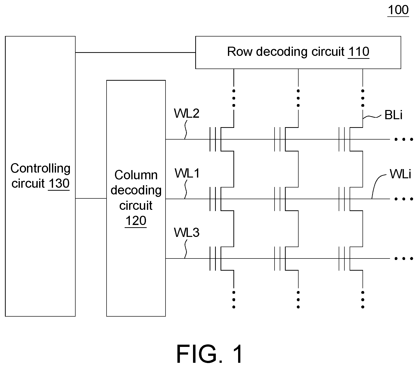
Please refer to , which shows a schematic diagram of a memory device 100 according to an embodiment. The memory device 100 is, for example, a NAND flash memory. The memory device 100 includes a plurality of bit lines BLi, a plurality of word lines WLi, a row decoding circuit 110 , a column decoding circuit 120 and a controlling circuit 130 . The word lines WLi include a first word line WL 1 , a second word line WL 2 and a third word line WL 3 which are adjacent. The second word line WL 2 and the third word line WL 3 are adjacent to the first word line WL 1 , and located at two sides of the first word line WL 1 .
The row decoding circuit 110 is coupled to the bit lines BLi. The column decoding circuit 120 is coupled to the word lines WLi. The controlling circuit 130 is coupled to the row decoding circuit 110 and the column decoding circuit 120 . The controlling circuit 130 is used to control the voltages applied to the bit line BLi and the word lines WLi to execute an erase procedure, a programming procedure or a read procedure.
Please refer to , which illustrates the threshold voltage shift of a plurality of memory cells according to an embodiment. Taking Triple Level Cell (TLC) for storing 8-bits data as an example, the memory cells have 8 states: an erase state E, a first programming state P 1 , a second programming state P 2 , a third programming state P 3 , a fourth programming state P 4 , and a fifth programming state P 5 , a sixth programming state P 6 and a seventh programming state P 7 . The threshold voltages of the erase state E, the first programming state P 1 , the second programming state P 2 , the third programming state P 3 , the fourth programming state P 4 , the fifth programming state P 5 , the sixth programming state P 6 and the seventh programming state P 7 increase in sequence. In one embodiment, the erase state E and the first programming state P 1 may be grouped into a low level state group G_L; the second programming state P 2 , the third programming state P 3 , the fourth programming state P 4 and the fifth programming state P 5 may be grouped into a median quasi-state group G_M; the sixth programming state P 6 and the seventh programming state P 7 may be grouped into a high level state group G_H. The low level state group G_L and the high level state group G_H belong to a state marginal group.
In another embodiment, the erase state E, the first programming state P 1 and the second programming state P 2 may be grouped into the low level state group G_L; the third programming state P 3 and the fourth programming state P 4 may be grouped into the median quasi-state group G_M; the fifth programming state P 5 , the sixth programming state P 6 and the seventh programming state P 7 may be grouped into the high level state group G_H. The low level state group G_L and the high level state group G_H belong to the state marginal group.
In another embodiment, the multi-level memory cells (MLCs) may be used to store 2-bits data, and have 4 states: the erase state, the first programming state, the second programming state and the third programming state. The threshold voltages of the erase state, the first programming state, the second programming state, the third programming state increase in sequence. The erase state may be grouped into the low level state group G_L; the first programming state and the second programming state may be grouped into the median quasi-state group G_M; the third programming state may be grouped into the high level state group G_H. The low level state group G_L and the high level state group G_H belong to the state marginal group.
In another embodiment, the Quad-level memory cells (QLCs) may be used to store 4-bits data, and have 16 states: the erase state, the first programming state, the second programming state, the third programming state, the fourth programming state, the fifth programming state, the sixth programming state, the seventh programming state, an eighth programming state, a ninth programming state, a tenth programming state, an eleventh programming state, a twelfth programming state, a thirteenth programming state, a fourteenth programming state and a fifteenth programming state. The threshold voltages of the erase state, the first programming state, the second programming state until the fifteenth programming state increase in sequence. The erase state and the first programming state to the fourth programming state may be grouped into the low level state group G_L; the fifth programming state to the tenth programming state may be grouped into the median quasi-state group G_M; the eleventh programming state to the fifteenth programming state may be grouped into the high level state group G_H. The low level state group G_L and the high level state group G_H belong to the state marginal group.
The number of bits of the memory cells is not used to limit the present technology. In another embodiment, the memory cells may have various numbers of erase/program states.
Refer back to . When the memory cells are just programmed, the distribution curve C 0 of the erase state E, the first programming state P 1 , the second programming state P 2 , the third programming state P 3 , the fourth programming state P 4 , the fifth programming state P 5 , the sixth programming state P 6 and the seventh programming state P 7 are respectively located in the 8 intervals distinguished by the read voltages Vread 1 , Vread 2 , Vread 3 , Vread 4 , Vread 5 , Vread 6 , Vread 7 . Therefore, the data can be correctly read by using the read voltage Vread 1 , Vread 2 , Vread 3 , Vread 4 , Vread 5 , Vread 6 , Vread 7 .
However, after a long time of use, the memory cells will have a phenomenon of threshold voltage shift. As shown in , after a long time of use, the memory cells will have a shifted distribution curve C 1 . As shown in the distribution curve C 1 , the distribution curve C 1 of the memory cells belonging to the low level state group G_L has shifted to the right; the distribution curve C 1 of the memory cells belonging to the high level state group G_H has shifted to the left, resulting in a read error.
In this embodiment, the controlling circuit 130 reads memory cells first. If a reading error occurs, the memory cells belonging to the state marginal group will be re-read in a special way, and the data can be correctly read.
Please refer to , which shows a flow chart of a reading method of the memory device 100 according to an embodiment. The reading method of the memory device 100 includes a read procedure PD 1 and a re-read procedure PD 2 . The read procedure PD 1 includes steps S 110 to S 120 .
Please refer to , which illustrates an example of the read procedure PD 1 . The first word line WL 1 , the second word line WL 2 and the third word line WL 3 of the word lines WLi are taken as an example. In the step S 110 of the read procedure PD 1 , the controlling circuit 130 applies a read voltage Vread to the first word line WL 1 . The read voltage Vread is, for example, the aforementioned read voltage Vread 1 , Vread 2 , Vread 3 , Vread 4 , Vread 5 , Vread 6 , Vread 7 .
Then, in the step S 120 of the read procedure PD 1 , the controlling circuit 130 applies a first pass voltage Vpass 1 to the second word line WL 2 and the third word line WL 3 . The step S 110 and step S 120 of the read procedure PD 1 are executed at the same time. In the read procedure PD 1 , the second word line WL 2 and the third word line WL 3 are applied with the same first pass voltage Vpass 1 to turn on the memory cells connected to the second word line WL 2 and the third word line WL 3 .
In the read procedure PD 1 , as long as there is no threshold voltage shift in the memory cell, different data contents can be read according to different read voltages Vread. However, after a long time of use, the memory cells may have a phenomenon of threshold voltage shift.
In the step S 130 , the controlling circuit 130 determines whether a read error occurs. The controlling circuit 130 , for example, determines whether a reading error has occurred through an error checking operation. If the reading error has been occurred, then the process proceeds to the step S 140 .
In the step S 140 , the controlling circuit 130 determines whether the memory cells to be read belong to the state marginal group (that is, the low level state group G_L and the high level state group G_H). The low level state group G_L includes, for example, the erase state E and the first programming state P 1 . The high level state group G_H includes, for example, the sixth programming state P 6 and the seventh programming state P 7 . If the memory cells to be read belong to the state marginal group, the process proceeds to the re-read procedure PD 2 .
Please refer to , which illustrates an example of the re-read procedure PD 2 . The re-read procedure PD 2 includes steps S 150 to S 170 . In the step S 170 of the re-read procedure PD 2 , the controlling circuit 130 applies the read voltage Vread to the first word line WL 1 . In the read procedure PD 1 and the re-read procedure PD 2 , the read voltage Vread applied to the first word line WL 1 remains unchanged.
In the step S 160 of the re-read procedure PD 2 , the controlling circuit 130 applies a second pass voltage Vpass 2 to the second word line WL 2 . The second pass voltage Vpass 2 is different from the first pass voltage Vpass 1 .
In the step S 170 of the re-read procedure PD 2 , the controlling circuit 130 applies a third pass voltage Vpass 3 to the third word line WL 3 . The third pass voltage Vpass 3 is different from the first pass voltage Vpass 1 . The steps S 150 to S 170 of the re-read procedure PD 2 are executed simultaneously.
Through the second pass voltage Vpass 2 and the third pass voltage Vpass 3 , the threshold voltage of the memory cells connected to the first word line WL 1 will be changed, thereby eliminating the threshold voltage shift. For example, as shown in , when the memory cells are executed the re-read procedure P 2 of the present disclosure, the memory cells will have a distribution curve C 2 . The distribution curve C 2 of the memory cells belonging to the low level state group G_L has shifted to the left and returned to the correct range; the distribution curve C 2 of the memory cells belonging to the high level state group G_H has shifted to the right and returned to the correct range, so the data can be read correctly.
Please refer to , which shows the threshold voltage shift of the memory cells belonging to the low level state group G_L, suffered from interference, or program/erase (P/E) cycled cells according to an embodiment. After the memory device 100 is used for a long time, the distribution curve C 1 of the memory cells belonging to the low level state group G_L, suffered from interference, or program/erase (P/E) cycled has shifted to the right. In this embodiment, when the memory cells are executed the re-read procedure PD 2 of the present disclosure, the memory cells will have the distribution curve C 2 . The distribution curve C 2 of the memory cells belonging to the low level state group G_L, suffered from interference, or program/erase (P/E) cycled has shifted to the left and returned to the correct range, so the data can be read correctly.
Please refer to , which illustrates the re-read procedure PD 2 for the memory cells belonging to the low level state group G_L, suffered from interference, or program/erase (P/E) cycled. In this embodiment, the second pass voltage Vpass 2 equals the first pass voltage Vpass 1 plus an adjusting voltage ΔV, and the third pass voltage Vpass 3 equals the first pass voltage Vpass 1 plus the adjusting voltage ΔV. The adjusting voltage ΔV is, for example, 0.01% to 50% of the first pass voltage Vpass 1 . The second pass voltage Vpass 2 and the third pass voltage Vpass 3 are substantially identical. When reading the memory cells connected to the first word line WL 1 , the second pass voltage Vpass 2 and the third pass voltage Vpass 3 , which are higher than the first pass voltage Vpass 1 , are applied to the second word line WL 2 and the third word line WL 3 , so the memory cells connected to the first word line WL 1 becomes easy to be turned on and have the distribution curve C 2 that shifts to the left and returns to the correct range.
The adjusting voltage ΔV may be positively related to the cycle times of memory device 100 . Generally speaking, the higher the number of operations of the memory device 100 , the more serious the deviation of the distribution curve C 1 , so a higher adjusting voltage ΔV may be used.
The adjusting voltage ΔV may be positively related to the retention time of the memory device 100 . Generally speaking, the longer the data retention time of the memory device 100 is, the more serious the deviation of distribution curve C 1 is, so a higher adjusting voltage ΔV may be used.
The adjusting voltage ΔV may be adaptively related to the neighboring data patterns. The adjusting voltage ΔV may be positively related to the marginal degree of the state. Generally speaking, the erase state E is more marginal than the first programming state P 1 , and the shift of the distribution curve C 1 of the erase state E will be more serious than that of the distribution curve C 1 of the first programming state P 1 , so the adjusting voltage ΔV for the erase state E may be the highest and the adjusting voltage ΔV for the first programming state P 1 may be the next highest.
Please refer to , which shows the threshold voltage shift of the memory cells belonging to the high level state group G_H according to an embodiment. After the memory device 100 has been used for a long time, the distribution curve C 1 of the memory cells belonging to the high level state group G_H has shifted to the left. In this embodiment, when the memory cells are executed the re-read procedure PD 2 of the present disclosure, the memory cells will have the distribution curve C 2 . The distribution curve C 2 of the memory cells belonging to the high level state group G_L may be shifted to the right and returned to the correct range.
Please refer to , which illustrates the re-read procedure PD 2 for the memory cells belonging to the high level state group G_H. In this embodiment, the second pass voltage Vpass 2 equals the first pass voltage Vpass 1 minus the adjusting voltage ΔV, and the third pass voltage Vpass 3 equals the first pass voltage Vpass 1 minus the adjusting voltage ΔV. The adjusting voltage ΔV is, for example, 0.01% to 50% of the first pass voltage Vpass 1 . The second pass voltage Vpass 2 and the third pass voltage Vpass 3 are substantially identical. When reading the memory cells connected to the first word line WL 1 , the second pass voltage Vpass 2 and third pass voltage Vpass 3 , which are lower than the first pass voltage Vpass 1 , are applied to the second word line WL 2 and third word line WL 3 , so the memory cells connected to the first word line WL 1 becomes hard to be turned on and have the distribution curve C 2 that shifts to the right and returns to the correct range.
The adjusting voltage ΔV may be positively related to the operation times of the memory device 100 . Generally speaking, the higher the number of operations of the memory device 100 , the more serious the deviation of the distribution curve C 1 , so a higher adjusting voltage ΔV may be used.
The adjusting voltage ΔV may be positively related to the retention time of the memory device 100 . Generally speaking, the longer the data retention time of the memory device 100 is, the more serious the deviation of distribution curve C 1 is, so a higher adjusting voltage ΔV may be used.
The adjusting voltage ΔV may be adaptively related to the neighboring data patterns. Generally speaking, the seventh programming state P 7 is more marginal than the sixth programming state P 6 , and the shift of the distribution curve C 1 of the seventh programming state P 7 will more serious than that of the distribution curve C 1 of the sixth programming state P 6 , so the adjusting voltage ΔV for the seventh programming state P 7 may be the highest and the adjusting voltage ΔV for the sixth programming state P 6 may be the next highest.
Please refer to , which illustrates another example of the re-read procedure PD 2 for memory cells belonging to the low level state group G_L, suffered from interference, or program/erase (P/E) cycled. In this embodiment, the second pass voltage Vpass 2 equals the first pass voltage Vpass 1 plus an adjusting voltage ΔV 1 , and the third pass voltage Vpass 3 equals the first pass voltage Vpass 1 plus an adjusting voltage ΔV 2 . The adjusting voltage ΔV 1 is, for example, 0.01% to 50% of the first pass voltage Vpass 1 , and the adjusting voltage ΔV 2 is, for example, 0.01% to 50% of the first pass voltage Vpass 1 . For example, the adjusting voltage ΔV 1 is set according to the states of the memory cells connected to the second word line WL 2 ; the adjusting voltage/V 2 is set according to the states of the memory cells connected to the third word line WL 3 . Therefore, the adjusting voltage ΔV 1 may be different from the adjusting voltage ΔV 2 , and the second pass voltage Vpass 2 and the third pass voltage Vpass 3 may be different.
Please refer to , which illustrates another example of the re-read procedure PD 2 for the memory cells belonging to the high level state group G_H. In this embodiment, the second pass voltage Vpass 2 equals the first pass voltage Vpass 1 minus an adjusting voltage ΔV 1 ′, and the third pass voltage Vpass 3 equals the first pass voltage Vpass 1 minus the adjusting voltage ΔV 2 ′. The adjusting voltage ΔV 1 ′ is, for example, 0.01% to 50% of the first pass voltage Vpass 1 , and the adjusting voltage ΔV 2 ′ is, for example, 0.01% to 50% of the first pass voltage Vpass 1 . For example, the adjusting voltage ΔV 1 ′ is set according to the states of the memory cells connected to the second word line WL 2 ; the adjusting voltage ΔV 2 ′ is set according to the states of the memory cells connected to the third word line WL 3 . Therefore, the adjusting voltage ΔV 1 ′ may be different from the adjusting voltage ΔV 2 ′, the second pass voltage Vpass 2 and the third pass voltage Vpass 3 may be different.
Please refer to , which illustrates that in the low level state group G_L, suffer from interference, or program/erase (P/E) cycled, the re-read procedure PD 2 is only executed for some memory cells with read errors. After the memory device 100 has been used for a long time, the distribution curve C 2 of the memory cells belonging to the low level state group G_L, suffered from interference, or program/erase (P/E) cycled has shifted to the right. In this embodiment, the re-read procedure PD 2 is only executed for some memory cells with read errors (e.g., the right half of the distribution curve C 2 ). When the memory cells are executed the re-read procedure PD 2 disclosed in this disclosure, the memory cells will have a distribution curve C 3 . The right half of the distribution curve C 3 of the memory cells belonging to the low level state group G_L may be shifted to the left and returned to the correct range.
Please refer to , which illustrates that in the high level state group G_H, the re-read procedure PD 2 is only executed for some memory cells with read errors. After the memory device 100 has been used for a long time, the distribution curve C 2 of the memory cells belonging to the high level state group G_H has shifted to the left. In this embodiment, the re-read procedure PD 2 is only executed for some memory cells with read errors (e.g., the left half of the distribution curve C 2 ). When the memory cells are executed the re-read procedure PD 2 of the present disclosure, the memory cells will have the distribution curve C 3 . The left half of the distribution curve C 3 of the memory cells belonging to the high level state group G_H can be shifted to the right and returned to the correct region or right region.
According to the above embodiments, in the re-read procedure PD 2 , through the adjustment of the second pass voltage Vpass 2 and the third pass voltage Vpass 3 , the threshold voltage of the memory cells connected to the first word line WL 1 can be changed, thereby the threshold voltage shift due to retention, interference, or program/erase (P/E) cycles is mitigated and the data reading error rate is significantly reduced.
It will be apparent to those skilled in the art that various modifications and variations can be made to the disclosed embodiments. It is intended that the specification and examples be considered as exemplary only, with a true scope of the disclosure being indicated by the following claims and their equivalents.
Figures (8)
Citations
This patent cites (6)
- US2013/0301360
- US2014/0347935
- US2016/0343414
- US2020/0211653
- US2023/0085319
- US201214438