Semiconductor Device and Operating Method Thereof
Abstract
A semiconductor device includes a first memory cell and a second memory cell. The first memory cell is configured to store a first data bit at a first node when the first memory cell is turned on. The second memory cell is configured to store the first data bit when the first memory cell is turned off. The first memory cell comprises a first switch coupled to the first node, and the first switch is configured to transmit the first data bit to the second memory cell, and configured to be turned off when the first memory cell is turned off.
Claims (20)
1. A semiconductor device, comprising: a first memory cell configured to store a first data bit at a first node when the first memory cell is turned on; and a second memory cell configured to store the first data bit when the first memory cell is turned off, wherein the first memory cell comprises a first switch coupled to the first node, the first switch is configured to transmit the first data bit to the second memory cell, and configured to be turned off when the first memory cell is turned off, and the semiconductor device further comprises: a first conductive segment configured to store the first data bit; a first source/drain structure coupled to the first conductive segment; and a second source/drain structure configured to receive a bit line signal corresponding to the first data bit, and disposed above the first source/drain structure along a direction, wherein the first conductive segment is elongated along the direction to be interposed between two portions of the second source/drain structure.
8. A semiconductor device, comprising: a first conductive segment configured to store a first data bit; a first source/drain structure coupled to the first conductive segment; a first gate structure coupled to a first source/drain portion of the first source/drain structure and a second source/drain portion of the first source/drain structure; and a second source/drain structure configured to receive a bit line signal corresponding to the first data bit, and disposed above the first source/drain structure along a direction, wherein the first gate structure is configured to isolate the first source/drain portion and the second source/drain portion from each other during a first period and a second period, and is configured to couple the first source/drain portion and the second source/drain portion to each other during a third period between the first period and the second period, and the first conductive segment is elongated along the direction to be interposed between two portions of the second source/drain structure.
16. A method of operating a semiconductor device, comprising: during a first period, storing a first data bit and a second data bit by a first memory cell; during a second period, transmitting the first data bit through a first switch to a first node of a second memory cell; during the second period, transmitting the second data bit through a second switch to a second node of the second memory cell; and during a third period, turning off each of the first switch and the second switch, wherein the first period, the second period and the third period are arranged in order, the second data bit is complementary with the first data bit, a first terminal of the first memory cell receives a first voltage signal, and a second terminal of the first memory cell is coupled to the first switch, and the semiconductor device comprises: a first conductive segment configured to store the first data bit; a first source/drain structure coupled to the first conductive segment; and a second source/drain structure configured to receive a bit line signal corresponding to the first data bit, and disposed above the first source/drain structure along a direction, wherein the first conductive segment is elongated along the direction to be interposed between two portions of the second source/drain structure.
Show 17 dependent claims
2. The semiconductor device of claim 1 , wherein the first memory cell is further configured to store a second data bit at a second node when the first memory cell is turned on, the first memory cell comprises a second switch coupled to the second node, the second switch is configured to transmit the second data bit to the second memory cell, and configured to be turned off when the first memory cell is turned off, and the second data bit is complementary with the first data bit.
3. The semiconductor device of claim 1 , wherein the second memory cell comprises: a memory element configured to store the first data bit, wherein a first terminal of the memory element is coupled to the first switch, a second terminal of the memory element is configured to receive a voltage signal, the voltage signal has a first voltage level when the first switch is turned on, and has a second voltage level when the first switch is turned off, and the first voltage level is different from the second voltage level.
4. The semiconductor device of claim 1 , wherein the first memory cell further comprises: a second switch configured to transmit a voltage signal to the first node, wherein a first terminal of the second switch is configured to receive the voltage signal, and a second terminal of the second switch is coupled to the first node, in response to the voltage signal having a first voltage level, the first memory cell is turned on, and in response to the voltage signal having a second voltage level, each of the first memory cell and the first switch is turned off.
5. The semiconductor device of claim 4 , wherein the first switch is turned off before the second memory cell stores the first data bit.
6. The semiconductor device of claim 1 , wherein the first switch is further configured to transmit the first data bit from the second memory cell to the first node when the first memory cell is turned on.
7. The semiconductor device of claim 1 , wherein the first switch is turned off during a first period, the first switch is turned on to transmit the first data bit from the second memory cell to the first node during a second period, the first switch is further turned off during a third period, and the first period, the second and the third period are arranged in order.
9. The semiconductor device of claim 8 , further comprising: a second conductive segment coupled to the first source/drain portion, and configured to receive the first data bit from the second source/drain portion during the third period.
10. The semiconductor device of claim 9 , wherein during a fourth period, the first gate structure is configured to couple the first source/drain portion and the second source/drain portion to each other, to transmit the first data bit from the second conductive segment to the second source/drain portion, and the third period, the second period and the fourth period are arranged in order.
11. The semiconductor device of claim 10 , wherein after the fourth period, the first gate structure is configured to isolate the first source/drain portion and the second source/drain portion from each other.
12. The semiconductor device of claim 8 , further comprising: a second conductive segment configured to store a second data bit; a third source/drain structure coupled to the second conductive segment; and a second gate structure coupled to a third source/drain portion of the third source/drain structure and a fourth source/drain portion of the third source/drain structure, wherein the second gate structure is configured to isolate the third source/drain portion and the fourth source/drain portion from each other during the first period and the second period, and is configured to couple the third source/drain portion and the fourth source/drain portion to each other during the third period, and the second data bit is complementary with the first data bit.
13. The semiconductor device of claim 12 , further comprising: a memory cell coupled to the first source/drain portion and the third source/drain portion, and configured to store the first data bit and the second data bit during the second period.
14. The semiconductor device of claim 13 , wherein during a fourth period, the first gate structure is configured to couple the first source/drain portion and the second source/drain portion to each other, to transmit the first data bit from the memory cell to the second source/drain portion, during the fourth period, the second gate structure is configured to couple the third source/drain portion and the fourth source/drain portion to each other, to transmit the second data bit from the memory cell to the fourth source/drain portion, and the third period, the second period and the fourth period are arranged in order.
15. The semiconductor device of claim 14 , wherein after the fourth period, the first gate structure is configured to isolate the first source/drain portion and the second source/drain portion from each other, and the second gate structure is configured to isolate the third source/drain portion and the fourth source/drain portion from each other.
17. The method of claim 16 , further comprising: providing a second voltage signal to the first node; and during the second period, changing the second voltage signal from a first voltage level to a second voltage level, wherein a logic value of the first data bit corresponds to the second voltage level.
18. The method of claim 17 , further comprising: during a fourth period, storing the first data bit and the second data bit by the second memory cell; during a fifth period, transmitting the first data bit through the first switch to the first memory cell; and during a sixth period, turning off the first switch, wherein the second voltage signal has the first voltage level during the sixth period, and has the second voltage level during each of the fourth and the sixth periods.
19. The method of claim 18 , further comprising: during the fifth period, transmitting the second data bit through the second switch to the first memory cell; and during the sixth period, turning off the second switch.
20. The method of claim 18 , wherein the first period, the second period, the third period, the fourth period, the fifth period and the sixth period are arranged in order.
Full Description
Show full text →
BACKGROUND
A Non-volatile memory (NVM) is a type of memory that can retain stored information even after power is removed. In contrast, volatile memory needs constant power in order to retain data. A static random-access memory (SRAM) is a typical volatile memory and may be coupled to the NVM to backup data bit when the SRAM is power-off.
BRIEF DESCRIPTION OF THE DRAWINGS
Aspects of the present disclosure are best understood from the following detailed description when read with the accompanying figures. It is noted that, in accordance with the standard practice in the industry, various features are not drawn to scale. In fact, the dimensions of the various features may be arbitrarily increased or reduced for clarity of discussion.
A is a schematic circuit diagram of a semiconductor device, in accordance with some embodiments of the present disclosure.
B is a timing diagram associated with the signals of the semiconductor device shown in A , in accordance with some embodiments of the present disclosure.
C is another timing diagram associated with the signals of the semiconductor device shown in A , in accordance with some embodiments of the present disclosure.
A is a schematic circuit diagram of a semiconductor device corresponding to the semiconductor device shown in A , in accordance with some embodiments of the present disclosure.
B is a timing diagram associated with the signals of the semiconductor device shown in A , in accordance with some embodiments of the present disclosure.
C is a timing diagram associated with the signals of the semiconductor device shown in A , in accordance with some embodiments of the present disclosure.
A is a layout diagram of a part of a semiconductor device corresponding to the memory cell shown in A and A , in accordance with some embodiments of the present disclosure.
B is a layout diagram of another part of the semiconductor device corresponding to the memory cell shown in A and A , in accordance with some embodiments of the present disclosure.
C is a cross section diagram of the semiconductor device along a line shown in A and B , in accordance with some embodiments of the present disclosure.
D is a cross section diagram of the semiconductor device along another line shown in A and B , in accordance with some embodiments of the present disclosure.
A is a layout diagram of a part of a semiconductor device corresponding to the semiconductor device shown in A , in accordance with some embodiments of the present disclosure.
B is a cross section diagram of the semiconductor device along a line shown in A , in accordance with some embodiments of the present disclosure.
is a schematic diagram of a semiconductor device corresponding to the semiconductor device shown in C and D , in accordance with some embodiments of the present disclosure.
DETAILED DESCRIPTION
The following disclosure provides many different embodiments, or examples, for implementing different features of the provided subject matter. Specific examples of components, materials, values, steps, arrangements or the like are described below to simplify the present disclosure. These are, of course, merely examples and are not intended to be limiting. Other components, materials, values, steps, arrangements or the like are contemplated. For example, the formation of a first feature over or on a second feature in the description that follows may include embodiments in which the first and second features are formed in direct contact, and may also include embodiments in which additional features may be formed between the first and second features, such that the first and second features may not be in direct contact. In addition, the present disclosure may repeat reference numerals and/or letters in the various examples. This repetition is for the purpose of simplicity and clarity and does not in itself dictate a relationship between the various embodiments and/or configurations discussed.
Further, spatially relative terms, such as “beneath,” “below,” “lower,” “above,” “upper” and the like, may be used herein for ease of description to describe one element or feature's relationship to another element(s) or feature(s) as illustrated in the figures. The spatially relative terms are intended to encompass different orientations of the device in use or operation in addition to the orientation depicted in the figures. The device may be otherwise oriented (rotated 90 degrees or at other orientations) and the spatially relative descriptors used herein may likewise be interpreted accordingly. The term mask, photolithographic mask, photomask and reticle are used to refer to the same item.
The terms applied throughout the following descriptions and claims generally have their ordinary meanings clearly established in the art or in the specific context where each term is used. Those of ordinary skill in the art will appreciate that a component or process may be referred to by different names. Numerous different embodiments detailed in this specification are illustrative only, and in no way limits the scope and spirit of the disclosure or of any exemplified term.
It is worth noting that the terms such as “first” and “second” used herein to describe various elements or processes aim to distinguish one element or process from another. However, the elements, processes and the sequences thereof should not be limited by these terms. For example, a first element could be termed as a second element, and a second element could be similarly termed as a first element without departing from the scope of the present disclosure.
In the following discussion and in the claims, the terms “comprising,” “including,” “containing,” “having,” “involving,” and the like are to be understood to be open-ended, that is, to be construed as including but not limited to. As used herein, instead of being mutually exclusive, the term “and/or” includes any of the associated listed items and all combinations of one or more of the associated listed items.
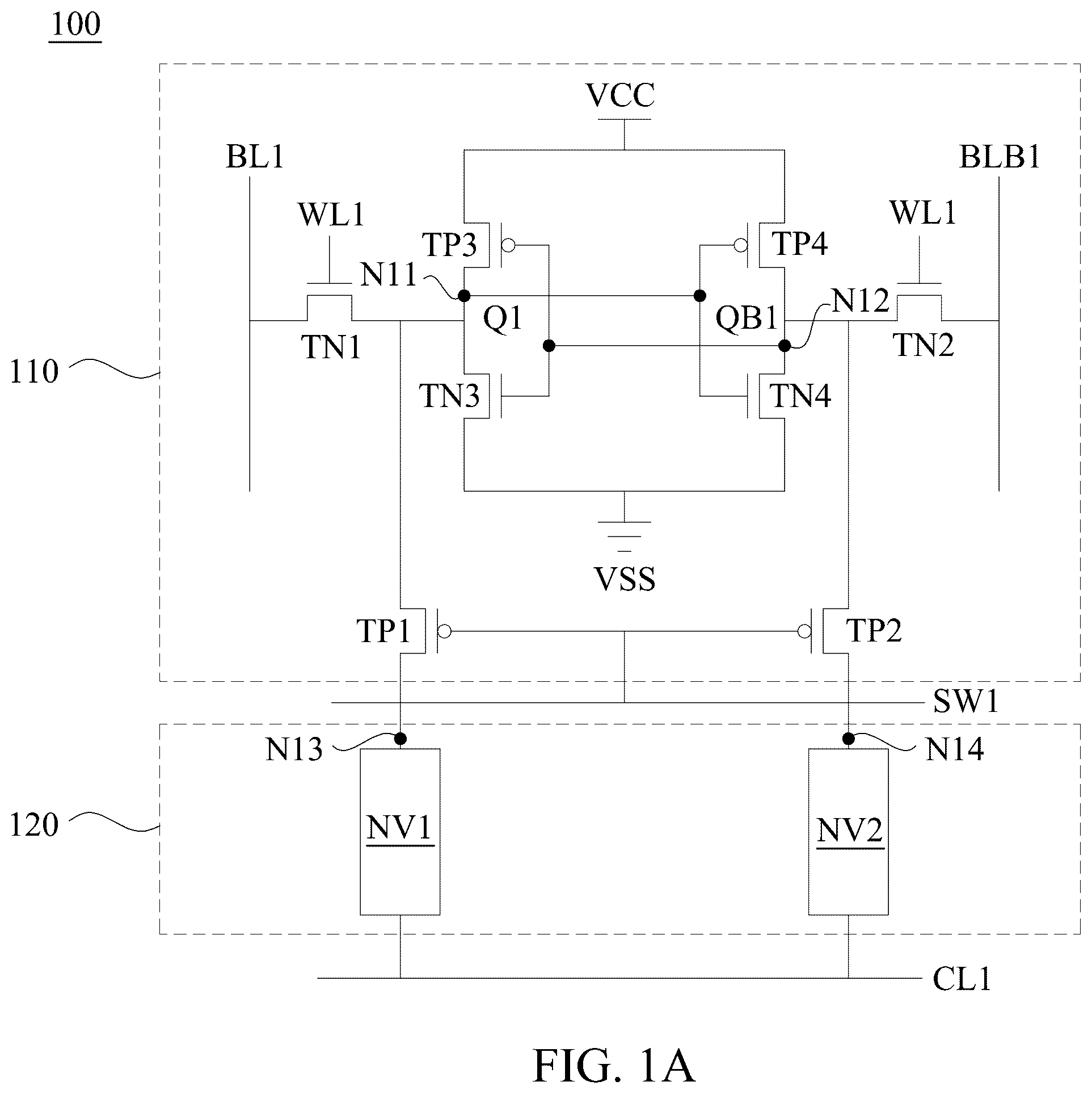
A is a schematic circuit diagram of a semiconductor device 100 , in accordance with some embodiments of the present disclosure.
As illustratively shown in A , the semiconductor device 100 includes memory cells 110 and 120 . In some embodiments, the semiconductor device 100 includes multiple memory cells (not shown in A ) arranged in rows and column, and is configured to store multiple data bits. In various embodiments, the other memory cells in the semiconductor device 100 have configurations similar with configurations of the memory cells 110 and 120 . The configurations of the memory cells 110 and 120 are described as follows.
In some embodiments, the memory cell 110 corresponds to a static random-access memory (SRAM), and the memory cell 120 corresponds to a nonvolatile memory (NVM), such as resistive random-access memory (RRAM), magnetic tunneling junction (MTJ), ferroelectric capacitor/field-effect transistor (FET), and/or silicon-oxide-nitride-oxide-silicon (SONOS).
As illustratively shown in A , the memory cell 110 includes switches TN 1 -TN 4 and TP 1 -TP 4 . A first terminal of the switch TN 1 is configured to receive a bit line signal BL 1 . A second terminal of the switch TN 1 is coupled to a node N 11 . A control terminal of the switch TN 1 is configured to receive a word line signal WL 1 . A first terminal of the switch TN 2 is configured to receive a bit line signal BLB 1 . A second terminal of the switch TN 2 is coupled to a node N 12 . A control terminal of the switch TN 2 is configured to receive the word line signal WL 1 . A first terminal of the switch TN 3 is configured to receive a reference voltage signal VSS. A second terminal of the switch TN 3 is coupled to the node N 11 . A control terminal of the switch TN 3 is coupled to the node N 12 . A first terminal of the switch TN 4 is configured to receive the reference voltage signal VSS. A second terminal of the switch TN 4 is coupled to the node N 12 . A control terminal of the switch TN 4 is coupled to the node N 11 .
As illustratively shown in A , a first terminal of the switch TP 1 is coupled to the node N 11 . A second terminal of the switch TP 1 is coupled to the memory cell 120 at a node N 13 . A control terminal of the switch TP 1 is configured to receive a control signal SW 1 . A first terminal of the switch TP 2 is coupled to the node N 12 . A second terminal of the switch TP 2 is coupled to the memory cell 120 at a node N 14 . A control terminal of the switch TP 2 is configured to receive the control signal SW 1 . A first terminal of the switch TP 3 is configured to receive a reference voltage signal VCC. A second terminal of the switch TP 3 is coupled to the node N 11 . A control terminal of the switch TP 3 is coupled to the node N 12 . A first terminal of the switch TP 4 is configured to receive the reference voltage signal VCC. A second terminal of the switch TP 4 is coupled to the node N 12 . A control terminal of the switch TP 4 is coupled to the node N 11 .
In some embodiments, in response to the reference voltage signal VCC having a voltage level VH, the memory cell 110 is turned on. In response to the reference voltage signal VCC having a voltage level VL, the memory cell 110 is turned off. In some embodiments, the reference voltage signal VSS is maintained at the voltage level VL. In some embodiments, the voltage level VH is higher than the voltage level VL. In some embodiments, the turning on and turning off of the memory cell 110 are referred to as power on and power off of the memory cell 110 .
In some embodiments, the memory cell 110 is configured to store a data bit Q 1 at the node N 11 , and store a complementary data bit QB 1 at the node N 12 . The data bits Q 1 and QB 1 are complementary to each other. In some embodiments, switches TN 1 -TN 4 and TP 1 -TP 4 are implemented by transistors of different conductive types. For example, the switches TN 1 -TN 4 are implemented by N-type metal-oxide-semiconductor (NMOS) transistors, and the switches TP 1 -TP 4 are implemented by P-type metal-oxide-semiconductor (PMOS) transistors. Accordingly, the switches TN 1 -TN 4 are turned on in response to the voltage level VH, and the switches TP 1 -TP 4 are turned on in response to the voltage level VL.
As illustratively shown in A , the memory cell 120 includes memory elements NV 1 and NV 2 . A first terminal of the memory element NV 1 is coupled to the second terminal of the switch TP 1 . A second terminal of the memory element NV 1 is configured to receive a voltage signal CL 1 . A first terminal of the memory element NV 2 is coupled to the second terminal of the switch TP 2 . A second terminal of the memory element NV 2 is configured to receive the voltage signal CL 1 .
In some embodiments, the switch TP 1 is configured to transmit the data bit Q 1 to the memory element NV 1 , such that the memory element NV 1 stores the data bit Q 1 at the node N 13 . Similarly, the switch TP 2 is configured to transmit the complementary data bit QB 1 to the memory element NV 2 , such that the memory element NV 2 stores the complementary data bit QB 1 at the node N 14 . In some embodiments, the memory elements NV 1 and NV 2 are configured to store the data bits Q 1 and QB 1 when the memory cell 110 is turned off.
In some embodiments, when the memory cell is turned on, the switch TP 1 is configured to transmit the data bit Q 1 from the memory element NV 1 to the node N 11 , and the switch TP 2 is configured to transmit the data bit QB 1 from the memory element NV 2 to the node N 12 , to restore a state of the memory cell 110 . Alternatively stated, the memory cell 120 is configured to backup data bits Q 1 and Q 2 for the memory cell 110 .
B is a timing diagram 101 associated with the signals of the semiconductor device 100 shown in A , in accordance with some embodiments of the present disclosure. As illustratively shown in B , the timing diagram 101 includes period P 11 -P 15 arranged continuously in order.
During the period P 11 , the reference voltage signal VCC has the voltage level VH, such that the memory cell 110 is turned on. The nodes N 11 and N 12 have voltage levels VH and VL, respectively. The data bit Q 1 has a first logic value corresponding to the voltage level VH, such as a logic value of 1. The data bit QB 1 has a second logic value corresponding to the voltage level VL, such as a logic value of 0. In response to the voltage level VL at the nodes N 12 , the switch TP 3 is turned on, to transmit the reference voltage signal VCC to the node N 11 . In response to the voltage level VH at the nodes N 11 , the switch TN 4 is turned on, to transmit the reference voltage signal VSS to the node N 12 .
On the other hand, during the period P 11 , the control signal SW 1 has the voltage level VL to turn off each of the switches TP 1 and TP 2 , such that the switch TP 1 isolates the memory element NV 1 from the node N 11 , and the switch TP 2 isolates the memory element NV 2 from the node N 12 . Accordingly, each of the nodes N 13 and N 14 has the voltage level VH. At this moment, the voltage signal CL 1 has the voltage level VL to deactivate the memory elements NV 1 and NV 2 .
In some embodiments, during the period P 11 , the memory cell 110 stores the data bits Q 1 and QB 1 normally. Accordingly, the period P 11 is referred to as a normal SRAM operation period. In some embodiments, during the normal SRAM operation period, the switches TN 1 and TN 2 are turned on to read or write the data bits Q 1 and QB 1 .
During the period P 12 , the control signal SW 1 is changed from the voltage level VH to the voltage level VL, such that each of the switches TP 1 and TP 2 is turned on. Accordingly, the switch TP 1 couples the node N 11 to the node N 13 , and the switch TP 2 couples the node N 12 to the node N 14 . The voltage signal CL 1 is changed from the voltage level VL to the voltage level VH to activate the memory elements NV 1 and NV 2 for a backup operation.
During the period P 13 , the switch TP 1 transmits the data bit Q 1 to the node N 13 and the switch TP 2 transmits the data bit QB 1 to the node N 14 , such that the node N 13 is maintained at the voltage level VH and the node N 14 is changed from the voltage level VH to the voltage level VL. Accordingly, the memory elements NV 1 and NV 2 store the data bits Q 1 and QB 1 , respectively. Alternatively stated, the memory elements NV 1 and NV 2 backup the data bits Q 1 and QB 1 .
During the period P 14 , the control signal SW 1 is changed from the voltage level VL to the voltage level VH, such that each of the switches TP 1 and TP 2 is turned off. The switch TP 1 isolates the memory element NV 1 from the node N 11 , and the switch TP 2 isolates the memory element NV 2 from the node N 12 . The voltage signal CL 1 is changed from the voltage level VH to the voltage level VL to deactivate the memory elements NV 1 and NV 2 from the backup operation.
In some embodiments, during the periods P 12 -P 14 , the memory cell 120 backups the data bits Q 1 and QB 1 . Accordingly, the periods P 12 -P 14 are referred to as a backup period.
During the period P 15 , the reference voltage signal VCC is changed from the voltage level VH to the voltage level VL, such that the memory cell 110 is turned off, and each of the nodes N 11 and N 12 is discharged to the voltage level VL. The control signal SW 1 is maintained at the voltage level VL, such that the switch TP 1 isolates the node N 13 from the node N 11 , and the switch TP 2 isolates the node N 14 from the node N 12 .
In some embodiments, during the period P 15 , the reference voltage signal VCC has the voltage level VL, such that the memory cell 110 is considered as power off. Accordingly, the period P 15 is referred to as a power off period.
In some approaches, an NVM cell is coupled directly to nodes of an SRAM cell storing data bits for backup the data bits. However, in such approaches, leakage currents flow from the nodes through the NVM cell and thus stability issues occur.
Compared to the above approaches, in some embodiments of the present disclosure, the switches TP 1 and TP 2 are turned off during the normal SRAM operation period and the power off period, to isolate the memory cell 120 from the memory cell 110 . Accordingly, leakage currents are reduced and the stability is increased.
C is another timing diagram 102 associated with the signals of the semiconductor device 100 shown in A , in accordance with some embodiments of the present disclosure. As illustratively shown in C , the timing diagram 102 includes period R 11 -R 17 arranged continuously in order.
During the period R 11 , the reference voltage signal VCC has the voltage level VL, such that the memory cell 110 is turned off. The nodes N 13 and N 14 have voltage levels VH and VL, respectively. Accordingly, the memory element NV 1 stores the data bit Q 1 having the first logic value, and the memory element NV 1 stores the data bit QB 1 having the second logic value.
In some embodiments, during the period R 11 , the reference voltage signal VCC has the voltage level VL, such that the memory cell 110 is considered as power off. Accordingly, the period R 11 is referred to as a power off period.
During the period R 12 , the reference voltage signal VCC is changed from the voltage level VL to the voltage level VH, such that the memory cell 110 is turned on. The control signal SW 1 has the voltage level VL to turn on each of the switches TP 1 and TP 2 , such that the nodes N 13 and N 14 are coupled to the nodes N 11 and N 12 , respectively. Accordingly, the switch TP 1 transmit the data bit Q 1 to the node N 11 , and the switch TP 2 transmit the data bit QB 1 to the node N 12 , such that the node N 11 is changed from the voltage level VL to the voltage level VH, and the node N 12 is maintained at the voltage level VL.
As described above, during the period R 12 , the memory cell 110 restores the data bits Q 1 and QB 1 at the nodes N 11 and N 12 from the memory cell 120 . Accordingly, in some embodiments, the period R 12 is referred to as a restore period.
During the period R 13 , the reference voltage signal VCC has the voltage level VH, and the memory cell 110 is turned on. The control signal SW 1 has the voltage level VH to turn off each of the switches TP 1 and TP 2 , such that the switch TP 1 isolates the node N 13 from the node N 11 , the switch TP 2 isolates the node N 14 from the node N 12 . At this moment, each of the nodes N 11 and N 13 has the voltage level VH, and each of the nodes N 12 and N 14 has the voltage level VL.
During the period R 14 , the voltage signal CL 1 is changed from the voltage level VL to the voltage level VH to activate the memory elements NV 1 and NV 2 for a reset operation.
During the period R 15 , the voltage signal CL 1 has the voltage level VH to reset the memory elements NV 1 and NV 2 . Accordingly, the node N 13 is maintained at the voltage level VH and the node N 14 is changed from the voltage level VL to the voltage level VH.
During the period R 16 , each of the nodes N 13 and N 14 is maintained at the voltage level VH. The voltage signal CL 1 is changed from the voltage level VH to the voltage level VL to terminate the reset operation. In some embodiments, the periods R 14 -R 16 are referred to as a reset period.
During the period R 17 , the reference voltage signal VCC has the voltage level VH, such that the memory cell 110 is turned on. The nodes N 11 and N 12 store the data bits Q 1 and QB 1 , respectively. In some embodiments, the period R 17 is referred to as a normal SRAM operation period.
Referring to B and C , in some embodiments, the operations of the periods P 11 -P 15 are performed before the operations of the periods R 11 -R 17 , and the periods P 15 and R 11 are arranged continuously in order. In other embodiments, the operations of the periods P 11 -P 15 are performed after the operations of the periods R 11 -R 17 , and the periods R 17 and P 11 are arranged continuously in order.
A is a schematic circuit diagram of a semiconductor device 200 corresponding to the semiconductor device 100 shown in A , in accordance with some embodiments of the present disclosure. Referring to A and A , the semiconductor device 200 is an alternative embodiment of the semiconductor device 100 . A follows a similar labeling convention to that of A . For brevity, the discussion will focus more on differences between A and A than on similarities.
Compared to the semiconductor device 100 , the memory cell 120 of the semiconductor device 200 is further configured to receive a voltage signal CL 2 . As illustratively shown in A , each of third terminals of the memory elements NV 1 and NV 2 is configured to receive the voltage signal CL 2 .
B is a timing diagram 201 associated with the signals of the semiconductor device 200 shown in A , in accordance with some embodiments of the present disclosure. As illustratively shown in B , the timing diagram 201 includes period P 21 -P 25 arranged continuously in order.
Referring to A , B , A and B , operations of the semiconductor device 200 during periods P 21 -P 25 are similar with the operations of the semiconductor device 100 during periods P 11 -P 15 . Therefore, some descriptions are not repeated for brevity.
During the periods P 21 -P 25 , the voltage signal CL 1 is maintained at the voltage level VL, to stabilize the memory cell 120 . During the period P 21 , voltage signal CL 2 has the voltage level VL to deactivate the memory elements NV 1 and NV 2 . During the period P 22 , the voltage signal CL 2 is changed from the voltage level VL to the voltage level VH to activate the memory elements NV 1 and NV 2 for a backup operation. During the period P 14 , the voltage signal CL 2 is changed from the voltage level VH to the voltage level VL to deactivate the memory elements NV 1 and NV 2 from the backup operation.
C is a timing diagram 202 associated with the signals of the semiconductor device 200 shown in A , in accordance with some embodiments of the present disclosure. As illustratively shown in C , the timing diagram 201 includes period R 21 -R 27 arranged continuously in order.
Referring to A , C , A and C , operations of the semiconductor device 200 during periods R 21 -R 27 are similar with the operations of the semiconductor device 100 during periods R 11 -R 17 . Therefore, some descriptions are not repeated for brevity.
During the periods R 21 -R 27 , the voltage signal CL 1 is maintained at the voltage level VL, to stabilize the memory cell 120 . During the period R 24 , the voltage signal CL 2 is changed from the voltage level VL to the voltage level VH to activate the memory elements NV 1 and NV 2 for a reset operation. During the period R 25 , the voltage signal CL 2 has the voltage level VH to reset the memory elements NV 1 and NV 2 . During the period R 26 , the voltage signal CL 2 is changed from the voltage level VH to the voltage level VL to terminate the reset operation.
A is a layout diagram of a part of a semiconductor device 300 corresponding to the memory cell 110 shown in A and A , in accordance with some embodiments of the present disclosure. A Z direction points out from the paper in A .
As illustratively shown in A , the semiconductor device 300 includes gate structures G 31 -G 34 , source/drain structures SD 31 , SD 32 and conductive segments CM 31 , CM 32 , CF 31 -CF 36 . Each of the source/drain structures SD 31 , SD 32 extends along an X direction. Each of the gate structures G 31 , G 32 and the conductive segments CF 31 -CF 33 extends along a Y direction and is overlapped with the source/drain structure SD 31 . Each of the gate structures G 33 , G 34 and the conductive segments CF 34 -CF 36 extends along the Y direction and is overlapped with the source/drain structure SD 31 . In some embodiments, the X direction, the Y direction and the Z direction are perpendicular with each other.
As illustratively shown in A , along the Y direction, the gate structures G 31 , G 32 and the conductive segments CF 31 -CF 33 are aligned with the gate structures G 33 , G 34 and the conductive segments CF 34 -CF 36 , respectively. The conductive segment CM 31 extends along the X direction, and is configured to couple the gate structure G 33 to the conductive segment CF 32 . The conductive segment CM 32 extends along the X direction, and is configured to couple the gate structure G 32 to the conductive segment CF 35 .
As illustratively shown in A , the source/drain structure SD 31 includes source/drain portions PF 31 -PF 33 arranged in order along the X direction. The source/drain structure SD 32 includes source/drain portions PF 34 -PF 36 arranged in order along the X direction. In some embodiments, the conductive segments CF 31 -CF 36 are coupled to the source/drain portions PF 31 -PF 36 , respectively.
Referring to A and A , in some embodiments, the switch TN 1 is implemented by the gate structure G 31 and the source/drain portions PF 31 , PF 32 . The switch TN 2 is implemented by the gate structure G 34 and the source/drain portions PF 35 , PF 36 . The switch TN 3 is implemented by the gate structure G 32 and the source/drain portions PF 32 , PF 33 . The switch TN 4 is implemented by the gate structure G 33 and the source/drain portions PF 34 , PF 35 .
Alternatively stated, the gate structure G 31 and the source/drain portions PF 31 , PF 32 are configured to operate as the switch TN 1 . The gate structure G 34 and the source/drain portions PF 35 , PF 36 are configured to operate as the switch TN 2 . The gate structure G 32 and the source/drain portions PF 32 , PF 33 are configured to operate as the switch TN 3 . The gate structure G 33 and the source/drain portions PF 34 , PF 35 are configured to operate as the switch TN 4 .
In such embodiments, the control terminals of the switches TN 1 -TN 4 correspond to the gate structures G 31 , G 34 , G 32 and G 33 , respectively. Each of the gate structures G 31 and G 34 is configured to receive the word line signal WL 1 . Each of the conductive segments CF 33 and CF 34 is configured to receive the reference voltage signal VSS. The conductive segments CF 31 and CF 36 are configured to receive the bit line signals BL 1 and BLB 1 , respectively. The gate structure G 33 and the conductive segments CM 31 , CF 32 correspond to the node N 11 . The gate structure G 32 and the conductive segments CM 32 , CF 35 correspond to the node N 12 .
B is a layout diagram of another part of the semiconductor device 300 corresponding to the memory cell 110 shown in A and A , in accordance with some embodiments of the present disclosure. The Z direction points out from the paper in B .
As illustratively shown in B , the semiconductor device 300 further includes conductive segments CB 31 -CB 34 , gate structures G 35 , G 36 and source/drain structures SD 33 , SD 34 . Each of the source/drain structures SD 33 and SD 34 extends along the X direction. Each of the conductive segments CB 31 -CB 34 extends along the Y direction. Each of the conductive segments CB 31 , CB 32 and the gate structures G 35 , G 32 is overlapped with the source/drain structure SD 33 . Each of the conductive segments CB 33 , CB 34 and the gate structures G 33 , G 36 is overlapped with the source/drain structure SD 34 .
As illustratively shown in B , the source/drain structure SD 33 includes source/drain portions PB 31 -PB 33 arranged in order along the X direction. The source/drain structure SD 34 includes source/drain portions PB 34 -PB 36 arranged in order along the X direction. In some embodiments, the conductive segments CB 31 -CB 34 are coupled to the source/drain portions PB 31 , PB 33 , PB 34 and PB 36 , respectively.
Referring to B and A , in some embodiments, the part shown in A is arranged above the part shown in B along the Z direction. The gate structure G 32 extends along the Z direction to be coupled to each of the source/drain structures SD 31 and SD 33 . The gate structure G 33 extends along the Z direction to be coupled to each of the source/drain structures SD 32 and SD 34 . The conductive segment CF 32 extends along the Z direction to be coupled to the source/drain portion PB 32 . The conductive segment CF 35 extends along the Z direction to be coupled to the source/drain portion PB 35 . Along the Z direction, the gate structures G 31 and G 35 are separated from each other, and the gate structures G 34 and G 36 are separated from each other. In some embodiments, the source/drain structures SD 31 and SD 32 are implemented by N-type material, and the source/drain structures SD 33 and SD 34 are implemented by P-type material.
Referring to A and B , in some embodiments, the switch TP 1 is implemented by the gate structure G 35 and the source/drain portions PB 31 , PB 32 . The switch TP 2 is implemented by the gate structure G 36 and the source/drain portions PB 35 , PB 36 . The switch TP 3 is implemented by the gate structure G 32 and the source/drain portions PB 32 , PB 33 . The switch TP 4 is implemented by the gate structure G 33 and the source/drain portions PB 34 , PB 35 .
Alternatively stated, the gate structure G 35 and the source/drain portions PB 31 , PB 32 are configured to operate as the switch TP 1 . The gate structure G 36 and the source/drain portions PB 35 , PB 36 are configured to operate as the switch TP 2 . The gate structure G 32 and the source/drain portions PB 32 , PB 33 are configured to operate as the switch TP 3 . The gate structure G 33 and the source/drain portions PB 34 , PB 35 are configured to operate as the switch TP 4 .
In such embodiments, the control terminals of the switches TP 1 -TP 4 correspond to the gate structures G 35 , G 36 , G 32 and G 33 , respectively. Each of the gate structures G 35 and G 36 is configured to receive the control signal SW 1 . Each of the conductive segments CB 32 and CB 33 is configured to receive the reference voltage signal VCC. The conductive segment CB 31 corresponds to the node N 13 and is coupled to the memory element NV 1 . The conductive segment CB 34 corresponds to the node N 14 and is coupled to the memory element NV 2 . The source/drain portion PB 32 and PB 35 correspond to the nodes N 11 and N 12 , respectively.
In the embodiments described above, when the control signal SW 1 has the voltage level VH, the gate structure G 35 isolates the source/drain portions PB 31 and PB 32 from each other, and the gate structure G 36 isolates the source/drain portions PB 35 and PB 36 from each other. As a result, the leakage currents flowing through the source/drain structures SD 33 and SD 34 are reduced.
On the other hand, when the control signal SW 1 has the voltage level VL, the gate structure G 35 couples the source/drain portions PB 31 and PB 32 to each other, and the gate structure G 36 couples the source/drain portions PB 35 and PB 36 to each other. Accordingly, the data bit Q 1 is able to be transmitted between the source/drain portions PB 31 and PB 32 , and the data bit QB 1 is able to be transmitted between the source/drain portions PB 35 and PB 36 .
C is a cross section diagram of the semiconductor device 300 along a line L 31 shown in A and B , in accordance with some embodiments of the present disclosure. The Y direction points into the paper in C .
As illustratively shown in C , the semiconductor device 300 further includes isolation structures IS 31 -IS 33 . The isolation structure IS 31 is formed between the source/drain portions PF 31 and PB 31 to isolate the source/drain portions PF 31 and PB 31 from each other. The isolation structure IS 32 is formed between the source/drain portions PF 32 and PB 32 to isolate the source/drain portions PF 32 and PB 32 from each other. The isolation structure IS 33 is formed between the source/drain portions PF 33 and PB 33 to isolate the source/drain portions PF 33 and PB 33 from each other. The conductive segment CF 31 extends through the source/drain portion PF 32 and the isolation structure IS 32 , to be coupled to the source/drain portion PB 32 .
D is a cross section diagram of the semiconductor device 300 along a line L 32 shown in A and B , in accordance with some embodiments of the present disclosure. The Y direction points into the paper in D .
As illustratively shown in D , the semiconductor device 300 further includes isolation structures IS 34 -IS 36 . The isolation structure IS 34 is formed between the source/drain portions PF 34 and PB 34 to isolate the source/drain portions PF 34 and PB 34 from each other. The isolation structure IS 35 is formed between the source/drain portions PF 35 and PB 35 to isolate the source/drain portions PF 35 and PB 35 from each other. The isolation structure IS 36 is formed between the source/drain portions PF 36 and PB 36 to isolate the source/drain portions PF 36 and PB 36 from each other. The conductive segment CF 35 extends through the source/drain portion PF 35 and the isolation structure IS 35 , to be coupled to the source/drain portion PB 35 .
A is a layout diagram of a part of a semiconductor device 400 corresponding to the semiconductor device 300 shown in A , in accordance with some embodiments of the present disclosure. The Z direction points out from the paper in A . As illustratively shown in A , the semiconductor device 400 includes memory cells 410 and 420 . Referring to A and A , in some embodiments, the memory cell 110 is implemented by one of the memory cells 410 and 420 , and another memory cell adjacent to the memory cell 110 is implemented by the other one of the memory cells 410 and 420 .
Referring to A and A , the semiconductor device 400 is an alternative embodiment of the semiconductor device 300 . A follows a similar labeling convention to that of A . For brevity, the discussion will focus more on differences between A and A than on similarities.
Compared to the semiconductor device 300 , the semiconductor device 400 further includes gate structures G 41 -G 44 and conductive segments CF 41 -CF 44 , CM 41 , CM 42 . The source/drain structure SD 31 further includes source/drain portions PF 41 and PF 42 . The source/drain structure SD 32 further includes source/drain portions PF 43 and PF 44 .
As illustratively shown in A , each of the gate structures G 41 , G 42 and the conductive segments CF 41 -CF 42 extends along the Y direction and is overlapped with the source/drain structure SD 31 . Each of the gate structures G 43 , G 44 and the conductive segments CF 43 -CF 44 extends along the Y direction and is overlapped with the source/drain structure SD 32 .
As illustratively shown in A , along the Y direction, the gate structures G 41 , G 42 and the conductive segments CF 31 -CF 32 are aligned with the gate structures G 43 , G 44 and the conductive segments CF 33 -CF 34 , respectively. The conductive segment CM 41 extends along the X direction, and is configured to couple the gate structure G 41 to the conductive segment CF 43 . The conductive segment CM 42 extends along the X direction, and is configured to couple the gate structure G 44 to the conductive segment CF 41 .
As illustratively shown in A , the source/drain portions PF 41 -PF 42 arranged in order along the X direction. The source/drain portions PF 43 -PF 44 arranged in order along the X direction. In some embodiments, the conductive segments CF 41 -CF 44 are coupled to the source/drain portions PF 41 -PF 44 , respectively.
Referring to A and A , in some embodiments, the switch TN 1 is implemented by the gate structure G 42 and the source/drain portions PF 41 , PF 42 . The switch TN 2 is implemented by the gate structure G 43 and the source/drain portions PF 43 , PF 36 . The switch TN 3 is implemented by the gate structure G 41 and the source/drain portions PF 41 , PF 33 . The switch TN 4 is implemented by the gate structure G 44 and the source/drain portions PF 43 , PF 44 .
In such embodiments, the control terminals of the switches TN 1 -TN 4 correspond to the gate structures G 42 , G 43 , G 41 and G 44 , respectively. Each of the gate structures G 42 and G 43 is configured to receive the word line signal WL 1 . Each of the conductive segments CF 33 and CF 44 is configured to receive the reference voltage signal VSS. The conductive segments CF 42 and CF 36 are configured to receive the bit line signals BL 1 and BLB 1 , respectively. The gate structure G 44 and the conductive segments CM 32 , CF 31 correspond to the node N 11 . The gate structure G 41 and the conductive segments CM 41 , CF 43 correspond to the node N 12 .
In some embodiments, each of the memory cells 410 and 420 corresponds to a circuit structure similar with the circuit structure of the memory cell 110 shown in A . The conductive segment CF 33 is configured to provide the reference voltage signal VSS to each of the memory cells 410 and 420 . The conductive segment CF 36 is configured to provide the bit line signal BLB 1 to each of the memory cells 410 and 420 . Alternatively stated, the memory cells 410 and 420 share the conductive segments CF 33 and CF 36 .
B is a cross section diagram of the semiconductor device 400 along a line L 41 shown in A , in accordance with some embodiments of the present disclosure. The Y direction points into the paper in A .
Referring to C and B , the semiconductor device 400 is an alternative embodiment of the semiconductor device 300 . B follows a similar labeling convention to that of C . For brevity, the discussion will focus more on differences between C and B than on similarities.
Compared to the semiconductor device 300 , the semiconductor device 400 further includes a gate structure G 45 , isolation structures IS 41 , IS 42 and a conductive segment CB 41 . The source/drain structure SD 33 further includes source/drain portions PB 41 and PB 42 .
As illustratively shown in B , the gate structure G 41 extends along the Z direction to be coupled to each of the source/drain portions PB 41 and PB 33 . The gate structure G 41 , the source/drain portion PB 41 , the gate structure G 45 and the source/drain portion PB 42 are arranged in order along the X direction. The gate structure G 45 is coupled to each of the source/drain portions PB 41 and PB 42 . The isolation structure IS 41 is formed between the source/drain portions PF 41 and PB 41 to isolate the source/drain portions PF 41 and PB 41 from each other. The isolation structure IS 42 is formed between the source/drain portions PF 42 and PB 42 to isolate the source/drain portions PF 42 and PB 42 from each other.
Referring to A and A , in some embodiments, the switch TP 2 is implemented by the gate structure G 41 and the source/drain portions PB 33 , PB 41 . The switch TP 4 is implemented by the gate structure G 45 and the source/drain portions PB 41 , PB 42 . In such embodiments, the control terminals of the switches TP 2 and TP 4 correspond to the gate structures G 41 and G 42 , respectively. The conductive segment CB 41 is configured to transmit the reference voltage signal VCC to the source/drain portion PB 42 .
is a schematic diagram of a semiconductor device 500 corresponding to the semiconductor device 300 shown in C and D , in accordance with some embodiments of the present disclosure. The Y direction points into the paper in .
As illustratively shown in , the semiconductor device 500 includes a memory cell 510 and conductive layers LF 50 -LF 59 , LB 50 -LB 55 . The conductive layers LB 55 , LB 54 , LB 53 , LB 52 , LB 51 , LB 50 , the memory cell 510 and the conductive layers LF 50 -LF 59 are arranged in order along the Z direction. Adjacent two of the conductive layers LF 50 -LF 59 and LB 50 -LB 55 are coupled to each other through vias. In some embodiments, the conductive layers LF 50 -LF 59 are formed by front side back-end-of-line (BEOL) process, and the conductive layers LB 50 -LB 55 are formed by back side BEOL process.
In some embodiments, each of the conductive layers LF 50 -LF 59 , LB 50 -LB 55 includes multiple conductive segments. The conductive segments in the conductive layers LB 54 , LB 52 , LB 50 , LF 50 , LF 52 , LF 54 , LF 56 and LF 58 extend along the Y direction. The conductive segments in the conductive layers LB 55 , LB 53 , LB 51 , LF 51 , LF 53 , LF 55 , LF 57 and LF 59 extend along the X direction.
In some embodiments, when a distance between a first conductive layer and the memory cell 510 is larger than a distance between a second conductive layer and the memory cell 510 , a size of the conductive segments in the first conductive layer is larger than a size of the conductive segments in the second conductive layer.
For example, a distance between the conductive layer LF 52 and the memory cell 510 is larger than a distance between the conductive layer LF 56 and the memory cell 510 . Accordingly, a size of the conductive segments in the conductive layer LF 52 is larger than a size of the conductive segments in the second conductive layer LF 56 .
As illustratively shown in , the memory cell 510 includes portions P 51 -P 53 arranged in order along the Z direction. The portion P 52 is sandwiched between the portions P 51 and P 53 . In some embodiments, the portion P 52 is formed by front-end-of-line (FEOL) process, and each of the portions P 51 and P 53 is formed by middle-of-line (MOL) process.
Referring to A , C , D and , in some embodiments, the memory cell 510 corresponds to the memory cell 110 , and has a structure similar with the structure shown in FIG. C and D . In such embodiments, the conductive segment CB 31 is coupled to the memory element NV 1 through at least a part of the conductive layers LF 50 -LF 59 and LB 50 -LB 55 , and the conductive segment CB 34 is coupled to the memory element NV 2 through at least a part of the conductive layers LF 50 -LF 59 and LB 50 -LB 55 . In some embodiments, the memory elements NV 1 and NV 2 are processed in the front side BEOL process or the back side BEOL process.
Also disclosed is a semiconductor device. The semiconductor device includes a first memory cell and a second memory cell. The first memory cell is configured to store a first data bit at a first node when the first memory cell is turned on. The second memory cell is configured to store the first data bit when the first memory cell is turned off. The first memory cell comprises a first switch coupled to the first node, and the first switch is configured to transmit the first data bit to the second memory cell, and configured to be turned off when the first memory cell is turned off.
Also disclosed is a semiconductor device. The semiconductor device includes a first conductive segment, a first source/drain structure and a first gate structure. The first conductive segment is configured to store a first data bit. The first source/drain structure is coupled to the first conductive segment. The first gate structure is coupled to a first source/drain portion of the first source/drain structure and a second source/drain portion of the first source/drain structure. The first gate structure is configured to isolate the first source/drain portion and the second source/drain portion from each other during a first period and a second period, and is configured to couple the first source/drain portion and the second source/drain portion to each other during a third period between the first period and the second period.
Also disclosed is a method of operating a semiconductor device. The method includes: during a first period, storing a first data bit and a second data bit by a first memory cell; during a second period, transmitting the first data bit through a first switch to a first node of a second memory cell; during the second period, transmitting the second data bit through a second switch to a second node of the second memory cell; and during a third period, turning off each of the first switch and the second switch. The first period, the second period and the third period are arranged in order, and the second data bit is complementary with the first data bit.
The foregoing outlines features of several embodiments so that those skilled in the art may better understand the aspects of the present disclosure. Those skilled in the art should appreciate that they may readily use the present disclosure as a basis for designing or modifying other processes and structures for carrying out the same purposes and/or achieving the same advantages of the embodiments introduced herein. Those skilled in the art should also realize that such equivalent constructions do not depart from the spirit and scope of the present disclosure, and that they may make various changes, substitutions, and alterations herein without departing from the spirit and scope of the present disclosure.
Figures (12)
Citations
This patent cites (4)
- US10672465
- US2019/0244666
- US2021/0158859
- US2021/0201998