Display Device and Method for Monitoring Operation of Pixels
Abstract
A display device may include a display panel including first and second pixels respectively connected to first and second sensing lines, a sensing driver including a sensing channel shared by the first and the second sensing lines, and a controller configured to control the display panel and the sensing driver. The controller may be configured to, in a first time period, electrically disconnect the sensing channel from the first and the second sensing lines, and reflect electrical characteristics of the first and the second pixels in the first and the second sensing lines, respectively, as sensing voltages, and in a second time period, record the sensing voltages reflected in the first and the second sensing lines in the sensing channel by time-sharing.
Claims (25)
1. A display device comprising: a display panel including first and second pixels respectively connected to first and second sensing lines; a sensing driver including a single sensing channel shared by the first and the second sensing lines; and a controller configured to control the display panel and the sensing driver, wherein the controller is further configured to: in a first time period, electrically disconnect the shared single sensing channel from the first and the second sensing lines and receive sensing voltages on respective ones of the first and the second sensing lines, the sensing voltages indicative of electrical characteristics of corresponding ones of the first and the second pixels; and in a second time period, selectively record the sensing voltages on the first and the second sensing lines in the shared single sensing channel, the sensing voltages selectively recorded by time-sharing the shared single sensing channel with the first and second sensing lines.
12. A display device comprising: a display panel including a plurality of rows of pixels connected to a plurality of sensing lines, the plurality of sensing lines being grouped into sensing line groups; a sensing driver including a single sensing channel for each sensing line group, each single sensing channel being shared by the sensing lines of the corresponding sensing line group; and a controller configured to control the display panel and the sensing driver, wherein the controller is further configured to: in a first time period, electrically disconnect each of the single sensing channels from the corresponding sensing line group and receive sensing voltages on the plurality of sensing lines that are indicative of electrical characteristics of the plurality of pixels; and in a second time period, record the sensing voltages of the sensing lines in each sensing line group in the corresponding single sensing channel by timing-sharing the single sensing channel with the sensing lines of the group.
17. A method of performing an operation of sensing electrical characteristics of pixels, wherein first and second pixels among the pixels are respectively connected to first and second sensing lines, the method comprising: receiving, in a first time period, sensing voltages on respective ones of the first and second sensing lines that are indicative of electrical characteristics of the first and the second pixels; electrically disconnecting a single sensing channel shared by the first and the second sensing lines from the first and the second sensing lines while the sensing voltages are received on the first and the second sensing lines; and in a second time period, connecting the first and the second sensing lines to the shared single sensing channel by time-sharing the shared single sensing channel with the first and second sensing lines, and successively recording the sensing voltages on the first and the second sensing lines in the shared single sensing channel.
19. An apparatus, comprising: a first sensing line coupled to a first pixel; a second sensing line coupled to a second pixel; and a shared single sensing channel selectively coupled to the first sensing line and the second sensing line, wherein, in a first time period, the shared single sensing channel is electrically disconnected from the first and second sensing lines, and the first and second sensing lines are respectively configured to receive first and second sensing voltages that are indicative of electrical characteristics of corresponding ones of the first and second pixels, wherein, in a second time period, the shared single sensing channel is selectively coupled to the first and second sensing lines and configured to record the first and second sensing voltages by time-sharing the shared single sensing channel with the first and second sensing lines.
Show 21 dependent claims
2. The display device according to claim 1 , wherein the controller is further configured to: initialize the sensing channel before the sensing voltage on the first sensing line is recorded in the sensing channel; and initialize the sensing channel before the sensing voltage on the second sensing line is recorded in the sensing channel.
3. The display device according to claim 1 , wherein: the sensing driver includes a first switch and a second switch, an input node of the sensing channel is connected to the first sensing line through the first switch and is connected to the second sensing line through the second switch, and the first and the second switches are turned off during the first time period.
4. The display device according to claim 3 , wherein: the sensing channel includes a sampling capacitor connected to the input node, and the sensing voltages on the first and the second sensing lines are recorded in the sampling capacitor by time-sharing the sensing channel with the first and second sensing lines.
5. The display device according to claim 4 , wherein the sensing channel is further configured to in response to control signals from the controller: initialize the sampling capacitor before the sensing voltage on the first sensing line is recorded in the sampling capacitor, and initialize the sampling capacitor before the sensing voltage on the second sensing line is recorded in the sampling capacitor.
6. The display device according to claim 4 , wherein the sensing channel comprises: a third switch configured to connect a first end of the sampling capacitor to the input node in response to a first control signal; a fourth switch configured to connect the first end of the sampling capacitor to an initialization voltage node in response to a second control signal; and a fifth switch configured to connect a second end of the sampling capacitor to a reference voltage node in response to a third control signal.
7. The display device according to claim 6 , wherein: the sensing channel comprises a reference capacitor, a first end of the reference capacitor is connected to the first end of the sampling capacitor, and the second end of the sampling capacitor and a second end of the reference capacitor correspond to output ends of the sensing channel.
8. The display device according to claim 1 , further comprising: a data driver connected to the first and the second pixels through first and second data lines, wherein: the controller controls the data driver, and the data driver is configured to: apply a first reference data voltage to the first and the second pixels through the first and the second data lines in the first time period; and apply a second reference data voltage lower than the first reference data voltage to the first and the second pixels through the first and the second data lines in the second time period.
9. The display device according to claim 1 , further comprising: a scan driver configured to operate under control of the controller, wherein: the display panel comprises a first switch connected between the first pixel and the first sensing line and a second switch connected between the second pixel and the second sensing line, and the scan driver is configured to transmit a sensing select signal to the first and the second switches, turn on the first and the second switches in the first time period, and turn off the first and the second switches before the second time period starts.
10. The display device according to claim 1 , further comprising: a scan driver configured to operate under control of the controller, wherein: the first and the second pixels are respectively connected to first and second data lines, each of the first and the second pixels comprises a switching transistor configured to transmit, in response to a scan signal, a voltage signal received through the corresponding data line to the corresponding pixel, and the scan driver is configured to provide the scan signal, turn on the switching transistor in the first time period, and turn off the switching transistor before the second time period starts.
11. The display device according to claim 1 , wherein the sensing driver comprises a data output circuit configured to output sensing data in response to each of the sensing voltages recorded in the sensing channel by time-sharing the sensing channel.
13. The display device according to claim 12 , wherein the controller is further configured to, before each time the sensing voltages of the sensing lines in each of the sensing line groups are recorded in the corresponding sensing channel by time-sharing, initialize the corresponding sensing channel.
14. The display device according to claim 12 , further comprising: a data driver connected to the plurality of pixels through a plurality of data lines, wherein: the controller is further configured to control the data driver, the data driver is configured to: in the first time period, apply a first reference data voltage to the plurality of pixels through the plurality of data lines; and in the second time period, apply a second reference data voltage lower than the first reference data voltage to the plurality of pixels through the plurality of data lines.
15. The display device according to claim 12 , further comprising: a scan driver configured to operate under control of the controller, wherein: the display panel includes a plurality of switches connected between the plurality of pixels and the plurality of sensing lines, and the scan driver is configured to transmit a sensing select signal to the plurality of switches, turn on the plurality of switches in the first time period, and turn off the plurality of switches before the second time period starts.
16. The display device according to claim 12 , further comprising: a scan driver configured to operate under control of the controller, wherein: the plurality of pixels are respectively connected to a plurality of data lines, each of the plurality of pixels comprises a switching transistor configured to transmit, in response to a scan signal, a voltage signal received through the corresponding data line to the corresponding pixel, and the scan driver is configured to provide the scan signal, turn on the switching transistor in the first time period, and turn off the switching transistor before the second time period starts.
18. The method according to claim 17 , further comprising: initializing the sensing channel before the sensing voltage reflected in the first sensing line is recorded in the sensing channel; and initializing the sensing channel before the sensing voltage reflected in the second sensing line is recorded in the sensing channel.
20. The apparatus of claim 19 , wherein the sensing channel includes a storage device to alternately store the first sensing voltage and the second sensing voltage.
21. The apparatus of claim 20 , further comprising: an initialization circuit configured to initialize the storage device before each of the first sensing voltage and the second sensing voltage are stored in the storage device.
22. The apparatus of claim 21 , wherein the storage device includes a sampling capacitor.
23. The apparatus of claim 21 , further comprising: an initialization circuit configured to initialize the first sensing line and the second sensing line.
24. The apparatus of claim 19 , further comprising: an output circuit configured to output sensing data that corresponds to the first and second sensing voltages.
25. The apparatus of claim 19 , wherein the electrical characteristics include threshold voltages of driving transistors of corresponding ones of the first and second pixels.
Full Description
Show full text →
CROSS-REFERENCE TO RELATED APPLICATION
The present application claims priority to Korean patent application number 10-2022-0127325, filed on Oct. 5, 2022, the entire disclosure of which is incorporated by reference herein in its entirety.
BACKGROUND
Field of Invention
Various embodiments of the present disclosure relate to an electronic device, and more particularly, to a display device and a method for monitoring the operation of pixels.
Description of Related Art
Various types of display devices have been developed. Examples include liquid crystal display devices and organic light emitting display devices. A display device includes a plurality of pixels which emit light to display images with various colors at various luminance levels. The pixels may include pixel circuits having substantially the same structure.
However, due to various reasons (e.g., process deviations, frequency of use of each pixel, degree of degradation of each pixel, etc.), mobility, threshold voltages of transistors of pixel circuits, and/or other electrical characteristics may differ from each other. In addition, light emitting diodes of the pixels may have deviations in threshold voltages thereof.
The information disclosed in this Background section is only for enhancement of understanding of the background of the described technology and therefore it may contain information that does not form the prior art that is already known to a person of ordinary skill in the art.
SUMMARY
An embodiment of the present disclosure may provide a display device including: a display panel including first and second pixels respectively connected to first and second sensing lines; a sensing driver including a sensing channel shared by the first and the second sensing lines; and a controller configured to control the display panel and the sensing driver. The controller may be configured to: in a first time period, electrically disconnect the sensing channel from the first and the second sensing lines, and reflect electrical characteristics of the first and the second pixels in the first and the second sensing lines, respectively, as sensing voltages; and in a second time period, record the sensing voltages reflected in the first and the second sensing lines in the sensing channel by time-sharing.
The controller may be configured to: initialize the sensing channel before the sensing voltage reflected in the first sensing line is recorded in the sensing channel; and initialize the sensing channel before the sensing voltage reflected in the second sensing line is recorded in the sensing channel.
The sensing driver may further include a first switch and a second switch. An input node of the sensing channel may be connected to the first sensing line through the first switch, and may be connected to the second sensing line through the second switch. The first and the second switches may be turned off during the first time period.
The sensing channel may include a sampling capacitor connected to the input node. The sensing voltages reflected in the first and the second sensing lines may be recorded in the sampling capacitor by time-sharing.
The sensing channel may be configured to, in response to control signals from the controller, initialize the sampling capacitor before the sensing voltage reflected in the first sensing line is recorded in the sampling capacitor, and initialize the sampling capacitor before the sensing voltage reflected in the second sensing line is recorded in the sampling capacitor.
The sensing channel may include: a third switch configured to connect a first end of the sampling capacitor to the input node in response to a first control signal; a fourth switch configured to connect the first end of the sampling capacitor to an initialization voltage node in response to a second control signal; and a fifth switch configured to connect a second end of the sampling capacitor to a reference voltage node in response to a third control signal.
The sensing channel may further include a reference capacitor. A first end of the reference capacitor may be connected to the first end of the sampling capacitor. The second end of the sampling capacitor and a second end of the reference capacitor may form output ends of the sensing channel.
The display device may further include a data driver connected to the first and the second pixels through first and second data lines. The controller may control the data driver. The data driver may be configured to: apply a first reference data voltage to the first and the second pixels through the first and the second data lines in the first time period; and apply a second reference data voltage lower than the first reference data voltage to the first and the second pixels through the first and the second data lines in the second time period.
The display device may further include a scan driver configured to operate under control of the controller. The display panel may further include a first switch connected between the first pixel and the first sensing line, and a second switch connected between the second pixel and the second sensing line. The scan driver may be configured to transmit a sensing select signal to the first and the second switches and turn on the first and the second switches in the first time period, and turn off the first and the second switches before the second time period starts.
The display device may further include a scan driver configured to operate under control of the controller. The first and the second pixels may be respectively connected to first and second data lines. Each of the first and the second pixels may include a switching transistor configured to transmit, in response to a scan signal, a voltage signal received through the corresponding data line to the corresponding pixel. The scan driver may be configured to provide the scan signal, turn on the switching transistor in the first time period, and turn off the switching transistor before the second time period starts.
The sensing driver further comprises a data output circuit configured to output sensing data in response to each of the sensing voltages recorded in the sensing channel by time-sharing.
An embodiment of the present disclosure may provide a display device including: a display panel including a plurality of rows of pixels connected to a plurality of sensing lines, the plurality of sensing lines being grouped into sensing line groups; a sensing driver including sensing channels respectively allocated to the sensing line groups; and a controller configured to control the display panel and the sensing driver. The controller may be configured to: in a first time period, electrically disconnect the sensing channels from the plurality of sensing lines, and reflect electrical characteristics of the plurality of pixels in the plurality of sensing lines as sensing voltages; and in a second time period, record the sensing voltages of the sensing lines included in each of the sensing line groups in the corresponding sensing channel by timing-sharing.
The controller may be configured to, before each time the sensing voltages of the sensing lines included in each of the sensing line groups are recorded in the corresponding sensing channel by time-sharing, initialize the corresponding sensing channel.
The display device may further include a data driver connected to the plurality of pixels through a plurality of data lines. The controller may be configured to control the data driver. The data driver may be configured to: in the first time period, apply a first reference data voltage to the plurality of pixels through the plurality of data lines; and in the second time period, apply a second reference data voltage lower than the first reference data voltage to the plurality of pixels through the plurality of data lines.
The display device may further include a scan driver configured to operate under control of the controller. The display panel may further include a plurality of switches connected between the plurality of pixels and the plurality of sensing lines. The scan driver may be configured to transmit a sensing select signal to the plurality of switches, turn on the plurality of switches in the first time period, and turn off the plurality of switches before the second time period starts.
The display device may further include a scan driver configured to operate under control of the controller. The plurality of pixels may be respectively connected to a plurality of data lines. Each of the plurality of pixels may include a switching transistor configured to transmit, in response to a scan signal, a voltage signal received through the corresponding data line to the corresponding pixel. The scan driver may be configured to provide the scan signal, turn on the switching transistor in the first time period, and turn off the switching transistor before the second time period starts.
An embodiment of the present disclosure may provide a method of performing an operation of sensing pixels. First and second pixels among the pixels are respectively connected to first and second sensing lines,
The method include: reflecting, in a first time period, electrical characteristics of the first and the second pixels in the first and the second sensing lines, respectively, as sensing voltages; electrically disconnecting a sensing channel shared by the first and the second sensing lines from the first and the second sensing lines while the sensing voltages are reflected in the first and the second sensing lines; and in a second time period, connecting the first and the second sensing lines to the sensing channel by time-sharing, and successively recording the sensing voltages reflected in the first and the second sensing lines in the sensing channel.
The method may further include: initializing the sensing channel before the sensing voltage reflected in the first sensing line is recorded in the sensing channel; and initializing the sensing channel before the sensing voltage reflected in the second sensing line is recorded in the sensing channel.
BRIEF DESCRIPTION OF THE DRAWINGS
illustrates an embodiment of a display device.
illustrates an embodiment of a portion of a display panel.
illustrates an embodiment of pixels.
illustrates an embodiment of a sensing driver.
illustrates an embodiment of a method of sensing electrical characteristics of pixels.
illustrates an embodiment of a portion of the sensing driver.
illustrates an embodiment of signals for the sensing driver.
to 14 illustrates examples of current flow pertaining to the sensing driver of .
illustrates an embodiment of signals for a sensing driver.
illustrates an embodiment of signals for a sensing driver.
illustrates an embodiment of a portion of a display panel.
illustrates an embodiment of a sensing driver.
DETAILED DESCRIPTION
As the present disclosure allows for various changes and numerous embodiments, particular embodiments will be illustrated in the drawings and described in detail in the written description. However, this is not intended to limit the present disclosure to particular modes of practice, and it is to be appreciated that all changes, equivalents, and substitutes that do not depart from the spirit and technical scope of the present disclosure are encompassed in the present disclosure.
It will be understood that, although the terms “first”, “second”, etc. may be used herein to describe various elements, these elements should not be limited by these terms. These terms are only used to distinguish one element from another element. For instance, a first element discussed below could be termed a second element without departing from the teachings of the present disclosure. Similarly, the second element could also be termed the first element. In the present disclosure, the singular forms are intended to include the plural forms as well, unless the context clearly indicates otherwise.
It will be further understood that the terms “comprise”, “include”, “have”, etc. when used in this specification, specify the presence of stated features, integers, steps, operations, elements, components, and/or combinations of them but do not preclude the presence or addition of one or more other features, integers, steps, operations, elements, components, and/or combinations thereof.
Features of the present disclosure, and methods for achieving the same will be cleared with reference to embodiments described later in detail together with the accompanying drawings. However, it is to be noted that the present disclosure is not limited to the embodiments but can be embodied in various other ways. In this specification, “connected/coupled” refers to one component not only directly coupling another component but also indirectly coupling another component through an intermediate component. In addition, in an embodiment of the present disclosure, the term “connection” between two components may embrace electrical connection and physical connection.
In accordance with one or more embodiments, a display device is provided in which two sensing lines share a single sensing channel (in order to reduce the surface area of the display device). Respective ones of the sensing lines carry voltages that reflect electrical characteristics of pixels under different sensing conditions (or different sensing schemes). The voltages may be selectively transmitted to a shared sensing channel to generate sensing data. Through these features, deterioration in the reliability of a sensing operation may be prevented, and any influence that may adversely affect a compensation value to be applied to driving conditions may also be prevented. As a result, the reliability of the display device may be significantly improved.
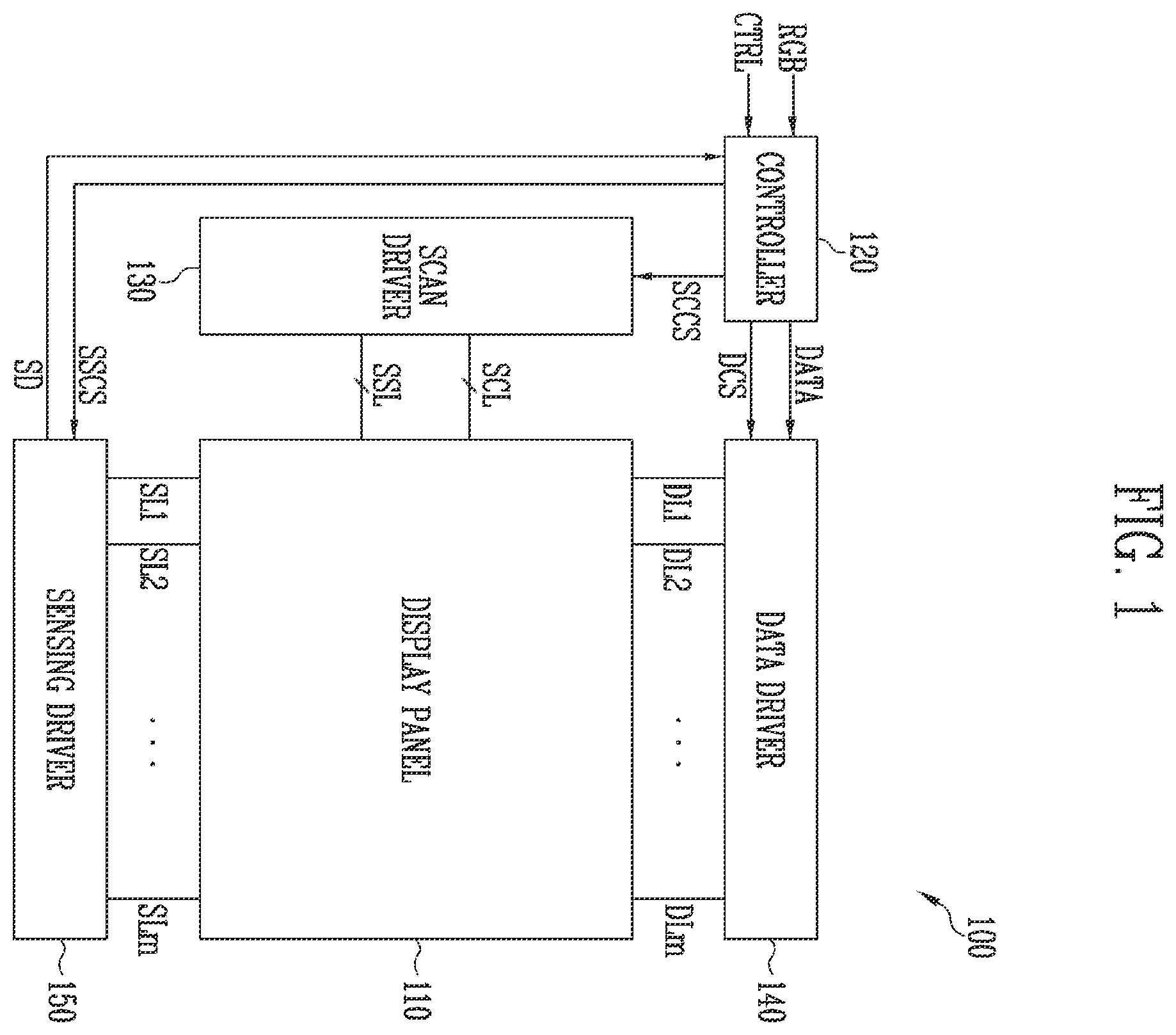
is a block diagram illustrating a display device 100 in accordance with an embodiment of the present disclosure.
Referring to , the display device 100 may include a display panel 110 , a controller 120 , a scan driver 130 , a data driver 140 , and a sensing driver 150 . The display panel 110 may include pixels which may be connected to the scan driver 130 by scan lines SCL and sensing select lines SSL. The pixels may be connected to the data driver 140 by first to m-th data lines DL 1 to DLm. The pixels may be connected to the sensing driver 150 by first to m-th sensing lines SL 1 to SLm.
The display panel 110 may be one of various types of display panels. Examples include a light emitting diode (LED) panel and a liquid crystal display panel (LCD). Hereinafter, there will be described the case where the pixels include light emitting diodes, and the display panel 110 is a light emitting diode panel. However, embodiments are not limited thereto, and the display panel 110 may be any one of other types of display panels.
The controller 120 may receive an image signal RGB and a control signal CTRL from an external device. The controller 120 may convert a data format of the image signal RGB to a format suitable for interface with the data driver 140 , and generate an image data signal DATA. The controller 120 may output a scan control signal SCCS, a data control signal DCS, and a sensing control signal SSCS based on the control signal CTRL.
The scan driver 130 may be connected to rows of pixels of the display panel 110 by the scan lines SCL. The scan driver 130 may apply scan signals to the scan lines SL in response to the scan control signal SCCS. Furthermore, the scan driver 130 may be connected to the rows of pixels of the display panel 110 by the sensing select lines SSL. During operations of sensing electrical characteristics of the pixels to be described in greater detail below, the scan driver 130 may apply a sensing select signal to the sensing select lines SSL in response to the scan control signal SCCS, and select each of the rows of pixels.
The data driver 140 may receive the data control signal DCS and the image data DATA from the controller 120 . The data driver 140 may output analog voltage signals to the first to m-th data lines DL 1 to DLm in response to the image data signal DATA. The analog voltage signals may correspond to grayscale values corresponding to the image data signal DATA. Hence, the analog voltage signals may be provided to the pixels of a row that receives a scan signal. The light emitting diodes of the corresponding pixels may emit light in response to the provided analog voltage signals.
The sensing driver 150 may receive the sensing control signal SSCS from the controller 120 . The sensing driver 150 may be connected to columns of the pixels of the display panel 110 by first to m-th sensing lines SL 1 to SLm. The sensing driver 150 may be configured to sense electrical characteristics of the pixels of a selected row through the first to m-th sensing lines SL 1 to SLm in response to the sensing control signal SSCS, and generate sensing data SD.
is a block diagram illustrating an embodiment of a portion of the display panel 110 of . In particular, illustratively shows pixels PX 1 to PXm connected to a first sensing select line SSL 1 among the sensing select lines SSL of .
Referring to , each of the first to m-th pixels PX 1 to PXm may be connected to the first to m-th sensing lines SL 1 to SLm of . The first to m-th sensing lines SL 1 to SLm of may be grouped into sensing lines groups. In embodiments, the first to m-th sensing lines SL 1 to SLm may be defined as sensing line pairs, each having two sensing lines. The first to m-th sensing lines SL 1 to SLm may be grouped into first to p-th sensing line groups SLG 1 to SLGp. Each sensing line group may include a plurality of (e.g., two) sensing lines connected to two adjacent pixels. In other embodiments, each sensing line group may include more than two sensing lines.
In accordance with one example, the first sensing line group SLG 1 may include an odd sensing line SL 1 _ 1 and an even sensing line SL 1 _ 2 . The odd sensing line SL 1 _ 1 may be connected to the first pixel PX 1 , and the even sensing line SL 1 _ 2 may be connected to the second pixel PX 2 . For example, the p-th sensing line group SLGp may include an odd sensing line SLp_ 1 and an even sensing line SLp_ 2 . The odd sensing line SLp_ 1 may be connected to the m−1-th pixel PXm−1, and the even sensing line SLp_ 2 may be connected to the m-th pixel PXm. Here, p is an integer of m/2.
The display panel 110 may include switches SSW 1 _ 1 , SSW 1 _ 2 , SSWp_ 1 , and SSWp_ 2 which respectively connect the first to m-th pixels PX 1 to PXm to the corresponding sensing lines. The switch SSW 1 _ 1 may connect the first pixel PX 1 to the odd sensing line SL 1 _ 1 of the first sensing line group SLG 1 in response to a sensing select signal of the first sensing select line SSL 1 . The switch SSW 1 _ 2 may connect the second pixel PX 2 to the even sensing line SL 1 _ 2 of the first sensing line group SLG 1 in response to a sensing select signal. The switch SSWp_ 1 may connect the m−1-th pixel PXm−1 to the odd sensing line SLp_ 1 of the p-th sensing line group SLGp in response to a sensing select signal. The switch SSWp_ 2 may connect the m-th pixel PXm to the even sensing line SLp_ 2 of the p-th sensing line group SLGp in response to a sensing select signal.
is a circuit diagram illustrating an embodiment of some of the pixels that are shown in . For convenience of explanation, illustrates the first and second pixels PX 1 and PX 2 of as a representative example, and the other pixels may have the same configuration.
Referring to , the first pixel PX 1 may include a plurality of transistors T 1 and T 2 , a capacitor C, and a light emitting diode LD. The switching transistor T 1 may connect a gate of the driving transistor T 2 to a first data line DL 1 in response to a scan signal of the first scan line SCL 1 , among the scan lines SCL of . The driving transistor T 2 may be connected between a first power supply VDD and an anode of the light emitting diode LD, and include a gate connected to one end of the switching transistor T 1 . The capacitor C may be connected between the gate of the driving transistor T 2 and the anode of the light emitting diode LD. The light emitting diode LD may include the anode connected to the driving transistor T 2 , and a cathode connected to a second power supply VSS. The switching transistor T 1 and the driving transistor T 2 may be NMOS transistors.
As illustrated in , the second pixel PX 2 may have the same or similar configuration as the configuration of the first pixel PX 1 . In other embodiments, the configurations may be different.
An odd sensing select transistor SST 1 _ 1 and an even sensing select transistor SST 1 _ 2 may be provided as the switch SSW 1 _ 1 and the switch SSW 1 _ 2 of , respectively. The odd sensing select transistor SST 1 _ 1 may be connected to the odd sensing line SL 1 _ 1 . The even sensing select transistor SST 1 _ 2 may be connected to the even sensing line SL 1 _ 2 . Gates of the odd sensing select transistor SST 1 _ 1 and the even sensing select transistor SST 1 _ 2 may be turned on in response to a sensing select signal applied to the first sensing select line SSL 1 . The odd and even sensing select transistors SST 1 _ 1 and SST 1 _ 2 may be NMOS transistors, but may have a different conductivity in another embodiment.
Electrical characteristics of the first and second pixels PX 1 and PX 2 may be respectively reflected in signals (e.g., sensing voltages) of the odd and even sensing lines SL 1 _ 1 and SL 1 _ 2 . A scan signal of the first scan line SCL 1 and a sensing select signal of the first sensing select line SSL 1 may be enabled to a first (e.g., high) logic level (hereinafter, a high level), so that a certain reference data voltage may be transmitted through the first and second data lines DL 1 and DL 2 . In this case, a voltage obtained by subtracting a threshold voltage of the driving transistor T 2 from the reference data voltage may be applied to a node between the driving transistor T 2 and the light emitting diode LD as a sensing voltage. The sensing voltage may be transmitted to the sensing line through the corresponding sensing select transistor. As such, the sensing voltage may include information about electrical characteristics of each pixel, for example, information about the threshold voltage of the driving transistor T 2 , as described above.
is a block diagram illustrating an embodiment of a sensing driver of . Referring to , a sensing driver 200 may include first to p-th sensing channels 211 to 21 p , a switch circuit 220 , and a data output circuit 230 .
The first to p-th sensing channels 211 to 21 p may be operated under control of the controller 120 of . The first to p-th sensing channels 211 to 21 p may be respectively allocated to the first to p-th sensing line groups SLG 1 to SLGp. Sensing lines that belong to each sensing line group may be connected to a corresponding (the same) sensing channel, and the corresponding sensing channel may be time-shared between the sensing lines. The odd and even sensing lines SL 1 _ 1 and SL 1 _ 2 of the first sensing line group SLG 1 may share the first sensing channel 211 . The odd and even sensing lines SLp_ 1 and SLp_ 2 of the p-th sensing line group SLGp may share the p-th sensing channel 21 p . As such, odd and even sensing lines SLi_ 1 and SLi_ 2 of an i-th sensing line group SLGi may share a first sensing channel 21 i (where i is an integer identical to or greater than 1 and less than or identical to p).
Each of the first to p-th sensing channels 211 to 21 p may be configured to sequentially record, therein, sensing voltages reflected in the corresponding odd and even sensing lines. In embodiments, each of the first to p-th sensing channels 211 to 21 p may include, for example, a sampling capacitor for recording a sensing voltage.
The sensing driver 200 may further include a line select switch connected between each of the odd and even sensing lines and the sensing channel that is shared by the odd and even sensing lines. An odd line select switch LSW 1 _ 1 may be connected between the odd sensing line SL 1 _ 1 of the first sensing line group SLG 1 and the first sensing channel 211 . An even line select switch LSW 1 _ 2 may be connected between the even sensing line SL 1 _ 2 of the first sensing line group SLG 1 and the first sensing channel 211 . Likewise, an odd line select switch LSWp_ 1 may be connected between the odd sensing line SLp_ 1 of the p-th sensing line group SLGp and the p-th sensing channel 21 p . An even line select switch LSWp_ 2 may be connected between the even sensing line SLp_ 2 of the p-th sensing line group SLGp and the p-th sensing channel 21 p . The odd line select switches LSW 1 _ 1 to LSWp_ 1 may be turned on or off in response to one or more select signals, e.g., in response to the same odd line select signal LSS 1 . The even line select switches LSW 1 _ 2 to LSWp_ 2 may be turned on or off in response to one or more select signals, e.g., in response to the same even line select signal LSS 2 .
In accordance with an embodiment of the present disclosure, when sensing voltages from the pixels are reflected in the sensing lines SL 1 _ 1 to SLp_ 1 and SL 1 _ 2 to SLp_ 2 of the first to p-th sensing line groups SLG 1 to SLGp, the odd line select switches LSW 1 _ 1 to LSWp_ 1 and the even line select switches LSW 1 _ 2 and LSWp_ 2 are turned off. Thereafter, each of the first to p-th sensing channels 211 to 21 p may be successively connected to the corresponding odd sensing line and the corresponding sensing line and record a corresponding sensing voltage therein. The first to p-th sensing channels 211 to 21 p may be initialized before each writing operation is performed. Hence, even though each of the first to p-th sensing channels 211 to 21 p is shared by the odd sensing line and the even sensing line of the corresponding sensing line group, sensing voltages may be recorded in the first to p-th sensing channels 211 to 21 p through the odd sensing lines SL 1 _ 1 to SLp_ 1 and the even sensing lines SL 1 _ 2 to SLp_ 2 with relatively high reliability.
The switch circuit 220 may be connected to the first to p-th sensing channels 211 to 21 p through the first to p-th channel output lines CHO 1 to CHOp, respectively. The switch circuit 220 may successively connect each of the first to p-th channel output lines CHO 1 to CHOp to the data output circuit 230 under control of the controller 120 . As such, the switch circuit 220 allows the first to p-th sensing channels 211 to 21 p to time-share the data output circuit 230 .
The data output circuit 230 may obtain sensing voltages recorded in the first to p-th sensing channels 211 to 21 p through the first to p-th channel output lines CHO 1 to CHOp, and output sensing data SD according to the obtained voltages.
The sensing driver 200 may further include first to p-th initialization circuits 241 to 24 p . The initialization circuits may control the voltage on the sensing lines to assume an initial (e.g., ground) value during a sensing operation for the display panel. The first to p-th initialization circuits 241 to 24 p may receive a line initialization signal LINT from the controller 120 . In response to the line initialization signal LINT, the first to p-th initialization circuits 241 to 24 p may respectively initialize the first to p-th sensing line groups SLG 1 to SLGp.
The odd and even line select signals LSS 1 and LSS 2 , a channel initialization signal CHINT, and the line initialization signal LINT may be included in the sensing control signal SSCS of .
is a flowchart illustrating a method of sensing electrical characteristics of pixels in accordance with an embodiment of the present disclosure. Hereinafter, for convenience of explanation, embodiments of the present disclosure will be described based on the first sensing channel 211 of the first to p-th sensing channels 211 to 21 p . The second to p-th sensing channels 212 to 21 p each may also have the same configuration as that of the first sensing channel 211 and be operated in the same manner as that of the first sensing channel 211 .
Referring to , at operation S 110 , the first sensing channel 211 is electrically disconnected (or interrupted) from the odd and even sensing lines SL 1 _ 1 and SL 1 _ 2 . The odd and even line select switches LSW 1 _ 1 and LSW 1 _ 2 may be turned off by disabling the odd and even line select signals LSS 1 and LSS 2 .
At operation S 120 , electrical characteristics of the first and second pixels PX 1 and PX 2 (refer to ), e.g., the threshold voltages of the driving transistors T 2 of the first and second pixels PX 1 and PX 2 , may be reflected in respective ones of the odd and even sensing lines SL 1 _ 1 and SL 1 _ 2 as sensing voltages. The electrical characteristics may correspond, for example, to threshold voltages of driving transistors in respective ones of the first and second pixels, mobility, and/or other parameters that are used, for example, to compensate for different electrical characteristics when the pixels are driven.
At operation S 130 , the first sensing channel 211 is initialized in response to a channel initialization signal CHINT. In embodiments, the first sensing channel 211 may include a sampling capacitor (refer to “SAMC” of ) provided to record a sensing voltage therein. The first sensing channel 211 may initialize the sampling capacitor before recording the sensing voltage. In one embodiment, operation S 130 may be performed before operation S 120 .
At operation S 140 , a sensing voltage reflected in the odd sensing line SL 1 _ 1 is recorded in the first sensing channel 211 , and a portion of sensing data SD is generated according to the recorded voltage.
At operation S 150 , the first sensing channel 211 is initialized in response to a channel initialization signal CHINT. In embodiments, the sampling capacitor of the first sensing channel 211 may be re-initialized.
At operation S 160 , a sensing voltage reflected in the even sensing line SL 1 _ 2 is recorded in the first sensing channel 211 , and a portion of sensing data SD is generated according to the recorded voltage.
As such, when sensing voltages are reflected in the odd and even sensing lines SL 1 _ 1 and SL 1 _ 2 , the first sensing channel 211 is electrically disconnected from the odd and even sensing lines SL 1 _ 1 and SL 1 _ 2 . Thereafter, the first sensing channel 211 may be successively connected to the odd and even sensing lines SL 1 _ 1 and SL 1 _ 2 so that the corresponding sensing voltage can be recorded therein. This may be accomplished by selectively activating corresponding ones of the odd and even line select switches LSW 1 _ 1 and LSW 1 _ 2 , as shown, for example, in the timing diagram of discussed in greater detail below. In one embodiment, the sampling capacitor may be initialized before the sensing voltages on the odd and even sensing lines SL 1 _ 1 and SL 1 _ 2 are recorded.
Each time a recording operation is performed, the first sensing channel 211 may be first initialized before the recording operation. Hence, even though the first sensing channel 211 is shared by the odd and even sensing lines SL 1 _ 1 and SL 1 _ 2 , the sensing voltages may be reflected in the odd and even sensing lines SL 1 _ 1 and SL 1 _ 2 with relatively high reliability, and may be recorded in the first sensing channel 211 .
is a block diagram illustrating an embodiment of a portion of the sensing driver of .
Referring to , a sensing driver 300 may include a sensing channel 310 , a switch circuit 320 , a data output circuit 330 , and an initialization circuit 340 . The sensing channel 310 , the switch circuit 320 , the data output circuit 330 , and the initialization circuit 340 may be respectively provided as the first sensing channel 211 , the switch circuit 220 , the data output circuit 230 , and the first initialization circuit 241 of . The second to p-th sensing channels 212 to 21 p of may also have the same configuration as that of the sensing channel 310 and be connected to the switch circuit 320 . Furthermore, the second to p-th initialization circuits 241 to 24 p of may have the same configuration as that of the initialization circuit 340 .
An odd sensing line capacitor SLC 1 may be connected between the odd sensing line SL 1 _ 1 and a ground node. The odd sensing line capacitor SLC 1 may be for conceptually showing a capacitance or a parasitic capacitance that is included in the odd sensing line SL 1 _ 1 . Alternatively, the odd sensing line capacitor SLC 1 may be a physical element connected to the odd sensing line SL 1 _ 1 . Likewise, an even sensing line capacitor SLC 2 may be connected between the even sensing line SL 1 _ 2 and a ground node. Each of the odd sensing line capacitor SLC 1 and the even sensing line capacitor SLC 2 may have a relatively large predetermined capacitance, compared to that of a sampling capacitor SAMC or a reference capacitor REFC of the sensing channel 310 .
The initialization circuit 340 may include first and second initialization switches ISW 1 and ISW 2 . The first initialization switch ISW 1 may be connected between an initialization power supply VINT and the odd sensing line SL 1 _ 1 , and may be turned on in response to a line initialization signal LINT. The second initialization switch ISW 2 may be connected between the initialization power supply VINT and the even sensing line SL 1 _ 2 , and may be turned on in response to a line initialization signal LINT.
The odd line select switch LSW 1 _ 1 may be provided between the odd sensing line SL 1 _ 1 and an input node IN of the sensing channel 310 , and may be turned on in response to an odd line select signal LSS 1 . The even line select switch LSW 1 _ 2 may be provided between the even sensing line SL 1 _ 2 and the input node IN, and may be turned on in response to an even line select signal LSS 2 .
The sensing channel 310 may include a sampling capacitor SAMC, a reference capacitor REFC, a sampling switch SAMSW, a comparison switch COMSW, and first to fourth switches SW 1 to SW 4 . In other embodiments, storage devices different from the aforementioned capacitors may be used.
The sampling capacitor SAMC may include a first end connected to the input node IN, and a second end connected to a first output node ON 1 of the sensing channel 310 . The sampling switch SAMSW may be connected between the input node IN and the first end of the sampling capacitor SAMC, and may be turned on in response to a sampling signal SAM.
A first end of the reference capacitor REFC may be connected to the first end of the sampling capacitor SAMC. A second end of the reference capacitor REFC may be connected to a second output node ON 2 of the sensing channel 310 . The first and second output nodes ON 1 and ON 2 may form a first channel output line CHO 1 of the sensing channel 310 .
The comparison switch COMSW may be connected between the first end of the sampling capacitor SAMC and the first end of the reference capacitor REFC, and may be turned on in response to a comparison signal COM.
The first switch SW 1 may be connected between the initialization power supply VINT and the first end of the sampling capacitor SAMC, and may transmit a voltage of the initialization power supply VINT to the first end of the sampling capacitor SAMC in response to a first capacitor initialization signal CPINT 1 . In other embodiments, the first switch SW 1 may be omitted, and the third switch SW 3 and the comparison switch COMSW may perform the function of the first switch SW 1 . In this case, when the comparison signal COM and the second capacitor initialization signal CPINT 2 are enabled, the third switch SW 3 and the comparison switch COMSW may transmit the voltage of the initialization power supply VINT to the first end of the sampling capacitor SAMC.
The second switch SW 2 may be connected between the second end of the sampling capacitor SAMC and a reference power supply VREF, and may be turned on in response to a reference signal SREF. In one or more embodiments, the reference power supply VREF and the initialization power supply VINT may be substantially the same as each other. In other embodiments, the reference power supply VREF and the initialization power supply VINT may be different from each other. The third switch SW 3 may be connected between the initialization power supply VINT and the first end of the reference capacitor REFC, and may be turned on in response to the second capacitor initialization signal CPINT 2 . The fourth switch SW 4 may be between the reference power supply VREF and the second output node ON 2 , and may be turned on in response to the reference signal SREF.
The line initialization signal LINT, the odd and even line select signals LSS 1 and LSS 2 , and the first and second capacitor initialization signals CPINT 1 and CPINT 2 , the comparison signal COM, and the reference signal SREF may be included in the sensing control signal SSCS output from the controller 120 of . In another embodiment, two or more of these control signals may be separately provided.
The switch circuit 320 may, for example, have the same configuration as that of the switch circuit 220 described with reference to . The switch circuit 320 may successively connect each of the first to p-th channel output lines CHO 1 to CHOp to the data output circuit 330 under control of the controller 120 (refer to ).
The data output circuit 330 may be operated under control of the controller 120 . The data output circuit 330 may include an analog-to-digital converter (ADC) 331 and a data output unit 332 . The ADC 331 may be connected to each channel output line, e.g., the first channel output line CHO 1 , through the switch circuit 320 . The ADC 331 may perform an analog-to-digital conversion operation for voltage differences between the first and second output nodes ON 1 and ON 2 of the connected channel output line, and thus generate sensing data SD. The data output unit 332 may output the sensing data SD generated by the ADC 331 . For example, the data output unit 332 may buffer the sensing data SD, and rearrange the buffered sensing data SD and output the rearranged sensing data SD to the controller 120 .
is a timing diagram illustrating signals pertaining to the sensing driver of in accordance with an embodiment of the method of sensing electrical characteristics of the pixels. to 14 are circuit diagrams conceptually illustrating a flow of current pertaining to the sensing driver of at some operations according to an embodiment of the method of sensing electrical characteristics of the pixels.
Referring to , at a first time t 1 , a reference data voltage is applied to each of the data lines DL 1 to DLm, a scan signal having a high level is applied to the first scan line SCL 1 , and a sensing select signal having a high level is applied to the first sensing select line SSL 1 .
At the first time t 1 , a line initialization signal LINT is in a state of having been enabled to a first (e.g., high) logic level. As illustrated in , the initialization circuit 340 may apply a voltage of the initialization power supply VINT to each of the odd and even sensing lines SL 1 _ 1 and SL 1 _ 2 in response to the line initialization signal LINT.
At a second time t 2 , the line initialization signal LINT is disabled to a second (e.g., low) logic level (hereinafter referred to as a low level). The initialization circuit 340 may separate the odd and even sensing lines SL 1 _ 1 and SL 1 _ 2 from the initialization power supply VINT. Referring to , sensing voltages according to the threshold voltages of the driving transistors T 2 of the first and second pixels PX 1 and PX 2 may be respectively reflected in the odd and even sensing lines SL 1 _ 1 and SL 1 _ 2 . In each of the first and second pixels PX 1 and PX 2 , a voltage obtained by subtracting the threshold voltage of the corresponding driving transistor T 2 from the reference data voltage may be applied to a node between the driving transistor T 2 and the light emitting diode LD as a sensing voltage. The corresponding sensing voltage may be reflected in the sensing line through the corresponding sensing select transistor. The odd and even sensing lines SL 1 _ 1 and SL 1 _ 2 may respectively have the odd and even sensing line capacitors SLC 1 and SCL 2 of . The odd and even sensing line capacitors SLC 1 and SCL 2 may maintain the reflected sensing voltages.
A preset time elapses from the second time t 2 , and the time reaches a fourth time t 4 . A period between the first time t 1 and the fourth time t 4 may be defined as a sensing period SP provided to reflect electrical characteristics of the pixels of the display panel 110 (refer to ) in the odd and even sensing lines SL 1 _ 1 and SL 1 _ 2 , as described above. The sensing period SP may be determined by taking into account the capacitances of the odd and even sensing line capacitors SLC 1 and SLC 2 . The sensing period SP may be relatively longer than a recording period RP.
Referring again to , all of the odd and even line select signals LSS 1 and LSS 2 are disabled to low levels during the sensing period SP, so that each of the odd and even sensing lines SL 1 _ 1 and SL 1 _ 2 may be electrically separated from the sensing channel 310 . Unlike the case where any one of the odd and even sensing lines SL 1 _ 1 and SL 1 _ 2 is electrically connected to the sensing channel 310 in at least a portion of the sensing period SP, the foregoing enables each of the odd and even sensing lines SL 1 _ 1 and SL 1 _ 2 to enter the recording period RP under substantially the same conditions. For example, each of the odd and even sensing lines SL 1 _ 1 and SL 1 _ 2 may be subsequently connected to the sensing channel 310 for substantially the same time in the recording period RP and transmit a sensing voltage to the sensing channel 310 . Hence, sensing voltages of the odd and even sensing lines SL 1 _ 1 and SL 1 _ 2 may be recorded in the sensing channel 310 with relatively high reliability.
At a third time t 3 before a recording period ORP (hereinafter, referred to as an odd recording period) for the sensing voltage reflected in the odd sensing line SL 1 _ 1 , the channel initialization signal CHINT (refer to ) is enabled to a predetermined (e.g., high) level in order to initialize the sensing channel 310 , e.g., in order to initialize the sampling capacitor of the sensing channel. For example, in accordance with one or more embodiments, the channel initialization signal CHINT may include a first capacitor initialization signal CPINT 1 . In embodiments, the channel initialization signal CHINT may include first and second capacitor initialization signals CPINT 1 and CPINT 2 . In response to the first capacitor initialization signal CPINT 1 having a high level, the first switch SW 1 may apply an initialization voltage VINT to the first end of the sampling capacitor SAMC. In response to the second capacitor initialization signal CPINT 2 having a high level, the third switch SW 3 may apply an initialization voltage VINT to the first end of the reference capacitor REFC. In embodiment, the reference signal SREF may be enabled to a high level. In response to the reference signal SREF having a high level, the second and fourth switches SW 2 and SW 4 may apply the reference voltage VREF to the second end of the sampling capacitor SAMC and the second end of the reference capacitor REFC.
Hence, as illustrated in , the initialization voltage VINT and the reference voltage VREF may be applied to the opposite ends of the sampling capacitor SAMC to initialize the sampling capacitor SAMC. The initialization voltage VINT and the reference voltage VREF may be applied to the opposite ends of the reference capacitor REFC to initialize the reference capacitor REFC.
At the fourth time t 4 , the odd line select signal LSS 1 is enabled to a high level, so that the sensing voltage of the odd sensing line SL 1 _ 1 is recorded in the sensing channel 310 . As such, the time for which the odd line select signal LSS 1 is enabled may be defined as an odd writing period ORP of the writing period RP.
Referring to , the odd line select switch LSW 1 _ 1 is turned on, and the sampling switch SAMSW is turned on in response to a sampling signal SAM having a high level. In embodiments, after the odd line select signal LSS 1 is enabled, the sampling signal SAM may be enabled during a predetermined (e.g., relatively short) time compared to that of the odd line select signal LSS 1 . Hence, the sensing voltage of the odd sensing line SL 1 _ 1 is transmitted to the first end of the sampling capacitor SAMC. The second and fourth switches SW 2 and SW 4 may remain turned on in response to the reference signal SREF. The third switch SW 3 may remain turned on in response to the second capacitor initialization signal CPINT 2 . As such, a voltage corresponding to a difference between the sensing voltage of the odd sensing line SL 1 _ 1 and the reference voltage VREF may be recorded in the sampling capacitor SAMC.
Referring again to , at a fifth time t 5 , the odd line select signal LSS 1 is disabled to a low level, so that recording is terminated. The voltage recorded in the sensing channel 310 may be provided to the data output circuit 330 . The data output circuit 330 may successively receive recorded voltages CH 1 to CHp from the first to p-th channel output lines CH 01 to CHOp (refer to ), and generate a first portion of the sensing data SD. The first portion of the generated sensing data SD may correspond to electrical characteristics of the pixels connected to the first to p-th odd sensing lines SL 1 _ 1 to SLp_ 1
Referring to , the odd line select switch LSW 1 _ 1 is turned off in response to an odd line select signal LSS 1 , so that the odd sensing line SL 1 _ 1 and the sensing channel 310 are electrically separated from each other. In embodiments, the sampling signal SAM is disabled, so that the sampling switch SAMSW may be turned off. The first and second capacitor initialization signals CPINT 1 and CPINT 2 and the reference signal SREF are disabled, so that the first to fourth switches SW 1 to SW 4 may be turned off. The comparison signal COM is enabled, so that the comparison switch COMSW may be turned off.
The first end of the sampling capacitor SAMC and the first end of the reference capacitor REFC may be connected to each other through the comparison switch COMSW and thus have substantially the same voltage. For example, the voltage of the first end of the sampling capacitor SAMC may be reduced to the foregoing same voltage. The voltage of the first end of the reference capacitor REFC may be increased to the foregoing same voltage. The second end of the sampling capacitor SAMC and the second end of the reference capacitor REFC may be in a floating state. Hence, the voltage of the second end of the sampling capacitor SAMC may vary depending on a voltage change (e.g., a voltage reduction) on the first end of the sampling capacitor SAMC.
The voltage of the second end of the reference capacitor REFC may vary depending on a voltage change (e.g., a voltage reduction) on the first end of the sampling capacitor SAMC. The difference in voltage between the second end of the sampling capacitor SAMC and the second end of the reference capacitor REFC may be a difference between the sensing voltage recorded in the first end of the sampling capacitor SAMC and the initialization voltage VINT. The difference between the sensing voltage and the initialization voltage VINT may be output to the data output circuit 330 through the first channel output line CHO 1 .
Referring again to , at a sixth time t 6 before a recording period ERP (hereinafter, referred to as an even recording period) for the sensing voltage reflected in the even sensing line SL 1 _ 2 , the channel initialization signal CHINT is enabled to a high level in order to re-initialize the sensing channel 310 . The sensing channel 310 may be operated in the same manner as that of the foregoing description pertaining to the third time t 3 . As illustrated in , the first to fourth switches SW 1 to SW 4 are turned on, so that the initialization voltage VINT and the reference voltage VREF may be applied to the opposite ends of the sampling capacitor SAMC. The initialization voltage VINT and the reference voltage VREF may be applied to the opposite ends of the reference capacitor REFC.
At a seventh time t 7 , the even line select signal LSS 2 is enabled to a high level, so that the sensing voltage of the even sensing line SL 1 _ 2 is recorded in the sensing channel 310 . As such, the time for which the even line select signal LSS 2 is enabled may be defined as an even writing period ERP of the writing period RP.
Referring to , the even line select switch LSW 1 _ 2 is turned on, and the sampling switch SAMSW is turned on in response to a sampling signal SAM having a high level. In embodiments, after the even line select signal LSS 2 is enabled, the sampling signal SAM may be enabled during a predetermined (e.g., relatively short) time compared to that of the even line select signal LSS 2 . As described above, because the sampling capacitor SAMC is initialized at the sixth time t 6 in the same manner as that of the third time t 3 , the sensing voltage of the even sensing line SL 1 _ 2 may be recorded in the first end of the sampling capacitor SAMC under substantially the same conditions as that of the odd sensing line SL 1 _ 1 . The second and fourth switches SW 2 and SW 4 may remain turned on in response to the reference signal SREF. The third switch SW 3 may remain turned on in response to the second capacitor initialization signal CPINT 2 . As such, a voltage corresponding to a difference between the sensing voltage of the even sensing line SL 1 _ 2 and the reference voltage VREF may be recorded in the sampling capacitor SAMC.
Referring again to , at an eighth time t 8 , the even line select signal LSS 2 is disabled to a low level, so that recording is terminated, and the voltage recorded in the sensing channel 310 may be provided to the data output circuit 330 . The data output circuit 330 may successively receive recorded voltages CH 1 to CHp from the first to p-th channel output lines CHO 1 to CHOp (refer to ), and generate a second portion of the sensing data SD. The second portion of the generated sensing data SD may correspond to electrical characteristics of the pixels connected to the first to p-th even sensing lines SL 1 _ 2 to SLp_ 2
Referring to , the even line select switch LSW 1 _ 2 is turned off in response to an even line select signal LSS 2 , so that the even sensing line SL 1 _ 2 and the sensing channel 310 are electrically separated from each other. In the same manner as described with reference to , the sensing voltage recorded in the first end of the sampling capacitor SAMC may be output through the first channel output line CHO 1 . For example, the sampling signal SAM is disabled, so that the sampling switch SAMSW may be turned off, the first to fourth switches SW 1 to SW 4 may be turned off, and the comparison switch COMSW may be turned on. Therefore, a difference in voltage between the second end of the sampling capacitor SAMC and the second end of the reference capacitor REFC may indicate a difference between the sensing voltage and the voltage of the initialization power supply VINT, and may be output to the data output circuit 330 through the first channel output line CHO 1 .
As such, the operation of connecting each of the odd and even sensing lines SL 1 _ 1 and SL 1 _ 2 to the sensing channel 310 and recording a corresponding sensing voltage in the sensing channel 310 may be performed after an initialization operation on the sensing channel 310 is performed. Hence, sensing voltages of the odd and even sensing lines SL 1 _ 1 and SL 1 _ 2 may be recorded in the sensing channel 310 under substantially the same conditions. Therefore, sensing data SD having enhanced reliability may be provided.
is a timing diagram illustrating signals pertaining to the sensing driver in accordance with another embodiment of the method of sensing the electrical characteristics of the pixels. The timing diagram of is the same as that of , except for the voltage signal of the data lines DL 1 to DLm. Hereinafter, repetitive explanations will be omitted.
Referring to , a first reference data voltage may be applied to the data lines DL 1 to DLm from the first time t 1 to the fourth time t 4 . At the fourth time t 4 , a second reference data voltage different from the first reference data voltage may be applied to the data lines DL 1 to DLm. In embodiments, the second reference data voltage may be different from (e.g., lower than) the first reference data voltage and, for example, be a data voltage corresponding to a black gray scale.
Referring to along with , at the fourth time t 4 , the switching transistors T 1 of the first and second pixels PX 1 and PX 2 may transmit the second reference data voltages of the first and second data lines DL 1 and DL 2 to the gates of the driving transistors T 2 in response to a scan signal of the first scan line SCL 1 . The odd and even sensing select transistors SST 1 _ 1 and SST 1 _ 2 may transmit (in response to a sensing select signal of the first sensing select line SSL 1 ) voltages of nodes between the second driving transistors T 2 and the light emitting diodes LE to the odd and even sensing lines SL 1 _ 1 and SL 1 _ 2 as sensing voltages. As the voltages of the first and second data lines DL 1 and DL 2 are reduced, the voltages of the nodes between the second driving transistors T 2 and the light emitting diodes LD may be reduced by the capacitors C.
In one embodiment, the driving transistors T 2 may be NMOS transistors. In this case, leakage current of the driving transistors T 2 may be reduced by the second reference data voltage being lower than the first reference data voltage. For example, gate-source voltages of the driving transistors T 2 may be reduced. Even though the even recording period ERP is later than the odd recording period ORP (for example, due to reduced leakage current of the driving transistors T 2 during a time difference between the even recording period ERP and the odd recording period ORP), the sensing voltage of the even sensing line SL 1 _ 2 is allowed to be recorded in the sensing channel 310 (refer to ) under conditions substantially identical or similar to that of the sensing voltage of the odd sensing line SL 1 _ 1 . Hence, sensing voltages of the odd and even sensing lines SL 1 _ 1 and SL 1 _ 2 may be recorded in the sensing channel 310 with relatively high reliability.
is a timing diagram illustrating signals pertaining to the sensing driver in accordance with another embodiment of the method of sensing electrical characteristics of the pixels. The timing diagram of is the same as that of , except for the scan signal of the first scan line SCL 1 and the sensing select signal of the first sensing select line SSL 1 . Hereinafter, repetitive explanations will be omitted.
Referring to , at the fourth time t 4 , the scan signal of the first scan line SCL 1 and the sensing select signal of the first sensing select line SSL 1 are disabled to predetermined (e.g., low) levels. Referring to along with , the switching transistors T 1 of the first and second pixels PX 1 and PX 2 are turned off in response to a disabled scan signal of the first scan line SCL 1 , and the odd and even sensing select transistors SST 1 _ 1 and SST 1 _ 2 are turned off in response to a disabled sensing select signal of the first sensing select line SSL 1 .
Hence, before the recording period RP, each of the odd and even sensing lines SL 1 _ 1 and SL 1 _ 2 may be electrically separated from the corresponding pixel in the same manner, and thus may not receive a sensing voltage. In other words, each of the odd and even sensing lines SL 1 _ 1 and SL 1 _ 2 may receive a sensing voltage from the corresponding pixel during substantially the same time period. During the recording period RP, the odd and even sensing lines SL 1 _ 1 and SL 1 _ 2 are electrically separated from the first and second pixels PX 1 and PX 2 , but due to the odd and even sensing line capacitors SLC 1 and SCL 2 (refer to ) having relatively large capacitances, the sensing voltages that are maintained therein may be reliably recorded in the sensing channel 310 (refer to ). Consequently, electrical characteristics of the first and second pixels PX 1 and PX 2 may be recorded in the sensing channel 310 through the odd and even sensing lines SL 1 _ 1 and SL 1 _ 2 with relatively high reliability.
is a block diagram illustrating another embodiment of a portion of a display panel of . In , for convenience of explanation, only some of the pixels of the display panel 110 of are illustrated.
Referring to , four adjacent pixels PX 1 to PX 4 of the display panel 400 may be connected to four sensing lines SL 1 _ 1 , SL 1 _ 2 , SL 1 _ 3 , and SL 1 _ 4 of one sensing line group. The first to m-th sensing lines SL 1 to SLm of may be grouped. Each of the plurality of sensing lines groups may include two or more sensing lines. In , there is illustrated the case where the first sensing line group SLG 1 that is any one of the plurality of sensing line groups includes first to fourth sensing lines SL 1 _ 1 , SL 1 _ 2 , SL 1 _ 3 , and SL 1 _ 4 . It can be understood that the number of sensing lines included in each sensing line group can be increased or reduced.
The first sensing line SL 1 _ 1 may be connected to a first pixel PX 1 through a switch SSW 1 _ 1 . The second sensing line SL 1 _ 2 may be connected to a second pixel PX 2 through a switch SSW 1 _ 2 . The third sensing line SL 1 _ 3 may be connected to a third pixel PX 3 through a switch SSW 1 _ 3 . The fourth sensing line SL 1 _ 4 may be connected to a fourth pixel PX 4 through a switch SSW 1 _ 4 . The switches SSW 1 _ 1 , SSW 1 _ 2 , SSW 1 _ 3 , and SSW 1 _ 4 may be turned on in response to a sensing select signal of the first sensing select line SSL 1 .
is a block diagram illustrating an embodiment of the sensing driver connected with the display panel of . In , for convenience of explanation, there is illustrated a sensing channel 510 connected to the first sensing line group SLG 1 having the first to m-th sensing lines SL 1 to SLm of , and the other sensing channels are omitted. It can be understood that the other sensing channels may be respectively connected to second to q-th channel output lines CHO 2 to CHOq of .
Referring to , a sensing driver 500 may include a sensing channel 510 , a switch circuit 520 , a data output circuit 530 , and an initialization circuit 540 which are connected to the first sensing line group SLG 1 of .
The first to fourth sensing lines SL 1 _ 1 , SL 1 _ 2 , SL 1 _ 3 , and SL 1 _ 4 may time-share the sensing channel 510 . In this way, the sensing channel 510 may selectively receive signals (e.g., voltages) from the first to fourth sensing lines SL 1 _ 1 , SL 1 _ 2 , SL 1 _ 3 , and SL 1 _ 4 . To achieve the foregoing, the first to fourth sensing lines SL 1 _ 1 , SL 1 _ 2 , SL 1 _ 3 , and SL 1 _ 4 may be connected to the sensing channel 510 through first to fourth line select switches LSW 1 _ 1 to LSW 1 _ 4 , respectively. The first to fourth line select switches LSW 1 _ 1 to LSW 1 _ 4 may be turned on in response to first to fourth line select signals LSS 1 to LSS 4 .
The sensing channel 510 may be operated under control of the controller 120 (refer to ), and may record sensing voltages that are respectively reflected in the first to fourth sensing lines SL 1 _ 1 , SL 1 _ 2 , SL 1 _ 3 , and SL 1 _ 4 .
The switch circuit 520 may be operated under control of the controller 120 (refer to ), and may successively connect each of the first to q-th channel output lines CHO 1 to CHOp to the data output circuit 530 . The data output circuit 530 may receive voltages recorded in the respective sensing channels through the first to q-th channel output lines CHO 1 to CHOp, generate sensing data SD, buffer the sensing data SD, and output the sensing data SD.
The initialization circuit 540 may initialize the first to fourth sensing lines SL 1 _ 1 , SL 1 _ 2 , SL 1 _ 3 , and SL 1 _ 4 in response to a line initialization signal LINT. In , for convenience of explanation, there is illustrated the initialization circuit 540 connected to the first sensing line group SLG 1 . In embodiments, the sensing driver 500 may further include initialization circuits corresponding to the other sensing lines groups. In other embodiments, the initialization circuit 540 may initialize not only the first sensing line group SLG 1 but also one or more of the other sensing line groups.
As such, a larger number of sensing lines than two sensing lines (odd and even sensing lines) may share a single sensing channel. As described with reference to , during an operation of sensing the pixels, when sensing voltages are reflected in the sensing lines SL 1 _ 1 to SL 1 _ 4 of each sensing line group, the sensing channel 510 may be electrically disconnected from the sensing lines SL 1 _ 1 to SL 1 _ 4 . Thereafter, the sensing channel 510 may be connected to each of the sensing lines SL 1 _ 1 to SL 1 _ 4 , so that each time the corresponding sensing voltage is recorded an operation of initializing the sensing channel 510 may be first performed. In embodiments, as described with reference to , before entering the recording period RP, a reduced reference data voltage may be applied to the data lines DL 1 to DLm. In embodiments, as described with reference to , before entering the recording period RP, a scan signal of the first scan line SCL 1 and a sensing select signal of the first sensing select line SSL 1 may be disabled to low levels.
Various embodiments of the present disclosure may provide a display device and method for performing an operation of sensing pixels with enhanced reliability.
The effects of the present disclosure are not limited by the foregoing, and other various effects are anticipated herein. While various exemplary embodiments have been described above, those skilled in the art will appreciate that various modifications, additions and substitutions are possible, without departing from the scope and spirit of the present disclosure. Therefore, the embodiments disclosed in this specification are only for illustrative purposes rather than limiting the technical spirit of the present disclosure. The scope of the present disclosure must be defined by the accompanying claims. The embodiments may be combined to form additional embodiments.
Figures (18)
Citations
This patent cites (15)
- US10547316
- US10803810
- US11107404
- US11417284
- US2018/0083078
- US2018/0254009
- US2021/0150966
- US2021/0183299
- US10-1987078
- US10-2020-0029178
- US10-2020-0057295
- US10-2020-0077812
- US10-2021-0083946
- US10-2338948
- US10-2022-0033577