Driver and Display Device Including the Same
Abstract
A driver is disclosed that includes an input circuit that transmits an input signal to a first node in response to at least one of a clock signal and an inverted clock signal, and an inverter that generates an output signal based on a voltage of the first node. Each of the input circuit and the inverter includes a first transistor and a second transistor connected to each other, an active area of the first transistor and an active area of the second transistor include different materials, and a gate terminal of the second transistor is electrically connected to a semiconductor material spaced apart from the active area of the second transistor.
Claims (9)
1. A driver comprising: an input circuit that transmits an input signal to a first node in response to at least one of a clock signal and an inverted clock signal; and an inverter that generates an output signal based on a voltage of the first node, wherein each of the input circuit and the inverter includes a first transistor and a second transistor connected to each other, an active area of the first transistor and an active area of the second transistor include different materials, and a gate terminal of the second transistor is electrically connected to a semiconductor material spaced apart from the active area of the second transistor, wherein the gate terminal of the second transistor includes an upper gate terminal and a lower gate terminal, and the upper gate terminal is electrically connected to the lower gate terminal.
Show 8 dependent claims
2. The driver of claim 1 , wherein the semiconductor material is connected to the upper gate terminal and the lower gate terminal, and the upper gate terminal is electrically connected to the lower gate terminal through the semiconductor material.
3. The driver of claim 2 , wherein the semiconductor material is in Schottky contact with the upper gate terminal and the lower gate terminal.
4. The driver of claim 3 , wherein each of a work function of the upper gate terminal and a work function of the lower gate terminal is greater than a work function of the semiconductor material.
5. The driver of claim 2 , wherein the semiconductor material is in ohmic contact with the upper gate terminal and the lower gate terminal.
6. The driver of claim 1 , wherein the first transistor is a PMOS transistor, and the second transistor is an NMOS transistor.
7. The driver of claim 1 , wherein the active area of the first transistor includes a silicon semiconductor, and the active area of the second transistor includes an oxide semiconductor.
8. The driver of claim 1 , wherein the inverter includes: a first inverter that inverts a voltage of the first node and provides an inverted voltage to a second node; and a second inverter that inverts a voltage of the second node and generates the output signal.
9. An electronic device comprising: the driver of claim 1 ; and pixels electrically connected to the driver.
Full Description
Show full text →
CROSS-REFERENCE TO RELATED APPLICATION(S)
This application claims priority under 35 USC § 119 to Korean Patent Application No. 10-2023-0086550 filed on Jul. 4, 2023, in the Korean Intellectual Property Office (KIPO), the entire disclosure of which is incorporated by reference herein.
BACKGROUND
1. Field
Embodiments relate to a driver and a display device including the same.
2. Description of the Related Art
A driver of a display device (e.g., a gate driver or a light emitting driver) may sequentially provide signals (e.g., a gate signal or a light emitting signal) to pixels of a display panel row by row. To sequentially provide the signals row by row, the driver may be implemented in a form of a shift register including a plurality of stages.
Each stage of the driver may include a transistor including a silicon semiconductor or a transistor including an oxide semiconductor. The transistor including the silicon semiconductor has an advantage of supplying a stable driving current, and the transistor including the oxide semiconductor has an advantage of fast turn-on operation and excellent off-current characteristics.
SUMMARY
Embodiments may provide a driver with reduced power consumption.
Embodiments may provide a display device including the driver.
A driver according to an embodiment of the present disclosure includes an input circuit that transmits an input signal to a first node in response to at least one of a clock signal and an inverted clock signal, and an inverter that generates an output signal based on a voltage of the first node. Each of the input circuit and the inverter includes a first transistor and a second transistor connected to each other, an active area of the first transistor and an active area of the second transistor include different materials, and a gate terminal of the second transistor is electrically connected to a semiconductor material spaced apart from the active area of the second transistor.
In an embodiment, the gate terminal of the second transistor may include an upper gate terminal and a lower gate terminal, and the upper gate terminal may be electrically connected to the lower gate terminal.
In an embodiment, the semiconductor material may be connected to the upper gate terminal and the lower gate terminal, and the upper gate terminal may be electrically connected to the lower gate terminal through the semiconductor material.
In an embodiment, the semiconductor material may be in Schottky contact with the upper gate terminal and the lower gate terminal.
In an embodiment, each of a work function of the upper gate terminal and a work function of the lower gate terminal may be greater than a work function of the semiconductor material.
In an embodiment, the semiconductor material may be in ohmic contact with the upper gate terminal and the lower gate terminal.
In an embodiment, the first transistor may be a PMOS transistor, and the second transistor may be an NMOS transistor.
In an embodiment, the active area of the first transistor may include a silicon semiconductor, and the active area of the second transistor may include an oxide semiconductor.
In an embodiment, the inverter may include a first inverter that inverts a voltage of the first node and provides an inverted voltage to a second node, and a second inverter that inverts a voltage of the second node and generates the output signal.
A display device according to an embodiment of the present disclosure includes a substrate, a first active pattern disposed on the substrate, a first gate electrode disposed on the first active pattern, a semiconductor pattern disposed on the first gate electrode, and including a material different from a material of the first active pattern, a second active pattern disposed on the first gate electrode, spaced apart from the semiconductor pattern, and including a material different from the material of the first active pattern, and a second gate electrode disposed on the semiconductor pattern and the second active pattern, and connected to the semiconductor pattern through a first contact hole.
In an embodiment, the first active pattern may include a silicon semiconductor, and each of the semiconductor pattern and the second active pattern may include an oxide semiconductor.
In an embodiment, the display device may further include a third gate electrode disposed between the first gate electrode and the semiconductor pattern. The semiconductor pattern and the second active pattern may be disposed on a same layer.
In an embodiment, the semiconductor pattern may be in Schottky contact with the second gate electrode through the first contact hole, and may be in Schottky contact with the third gate electrode through a second contact hole.
In an embodiment, each of a work function of the second gate electrode and a work function of the third gate electrode may be greater than a work function of the semiconductor pattern.
In an embodiment, the second active pattern may be disposed on the semiconductor pattern, and the semiconductor pattern may be in Schottky contact with the second gate electrode through the first contact hole.
In an embodiment, the first active pattern may include a P-type impurity, and the second active pattern may include an N-type impurity.
A display device according to an embodiment of the present disclosure includes a substrate, a first active pattern disposed on the substrate, a first gate electrode disposed on the first active pattern, a second gate electrode disposed on the first gate electrode, a semiconductor pattern disposed on the second gate electrode, connected to the second gate electrode through a contact hole, and including a material different from a material of the first active pattern, a second active pattern disposed on a same layer as the semiconductor pattern, spaced apart from the semiconductor pattern, and including a material different from the material of the first active pattern, and a third gate electrode disposed on the semiconductor pattern and the second active pattern, spaced apart from the semiconductor pattern in a plan view, and electrically connected to the semiconductor pattern.
In an embodiment, the first active pattern may include a silicon semiconductor, and each of the semiconductor pattern and the second active pattern may include an oxide semiconductor.
In an embodiment, the semiconductor pattern may be in ohmic contact with the third gate electrode through the contact hole.
In an embodiment, the first active pattern may include a P-type impurity, and each of the semiconductor pattern and the second active pattern may include an N-type impurity.
In a driver according to embodiments of the present disclosure, a stage of the driver may include first, second, third, and fourth transistors including a silicon semiconductor and fifth, sixth, and seventh transistors including an oxide semiconductor. Each of the fifth, sixth, and seventh transistors may include an upper gate terminal, a lower gate terminal, and a semiconductor material. As the semiconductor material makes a Schottky contact or ohmic contact with the upper gate terminal and the lower gate terminal, a voltage applied to the lower gate terminal may be lowered, and a threshold voltage of each of the fifth, sixth, and seventh transistors may increase. In addition, since each of the fifth, sixth, and seventh transistors have a double gate structure, output current may increase. Therefore, the driver may require a relatively small number of buffer transistors, and thus a dead space of a display device including the driver may be reduced.
In addition, each of the first, second, third, and fourth transistors may be a PMOS transistor, and each of the fifth, sixth, and seventh transistors may be an NMOS transistor. As the stage of the driver includes a CMOS circuit, power consumption of the driver and the display device including the driver may be reduced.
BRIEF DESCRIPTION OF THE DRAWINGS
is a plan view illustrating a display device according to embodiments of the present disclosure.
is a block diagram illustrating the display device of .
is a block diagram illustrating a driver included in the display device of .
is a block diagram illustrating a stage of the driver of .
is a circuit diagram illustrating a stage of a driver according to an embodiment of the present disclosure.
is a graph illustrating a change in a threshold voltage of a transistor according to a voltage applied to a lower gate terminal of the transistor.
is a cross-sectional view illustrating an example of transistors included in the stage of .
is an enlarged plan view of area A of .
is a cross-sectional view illustrating another example of transistors included in the stage of .
is a circuit diagram illustrating a stage of a driver according to another embodiment of the present disclosure.
is a cross-sectional view illustrating an example of transistors included in the stage of .
DETAILED DESCRIPTION OF THE EMBODIMENTS
Hereinafter, embodiments of the present disclosure will be described in more detail with reference to the accompanying drawings. The same reference numerals are used for the same components in the drawings, and redundant descriptions of the same components will be omitted.
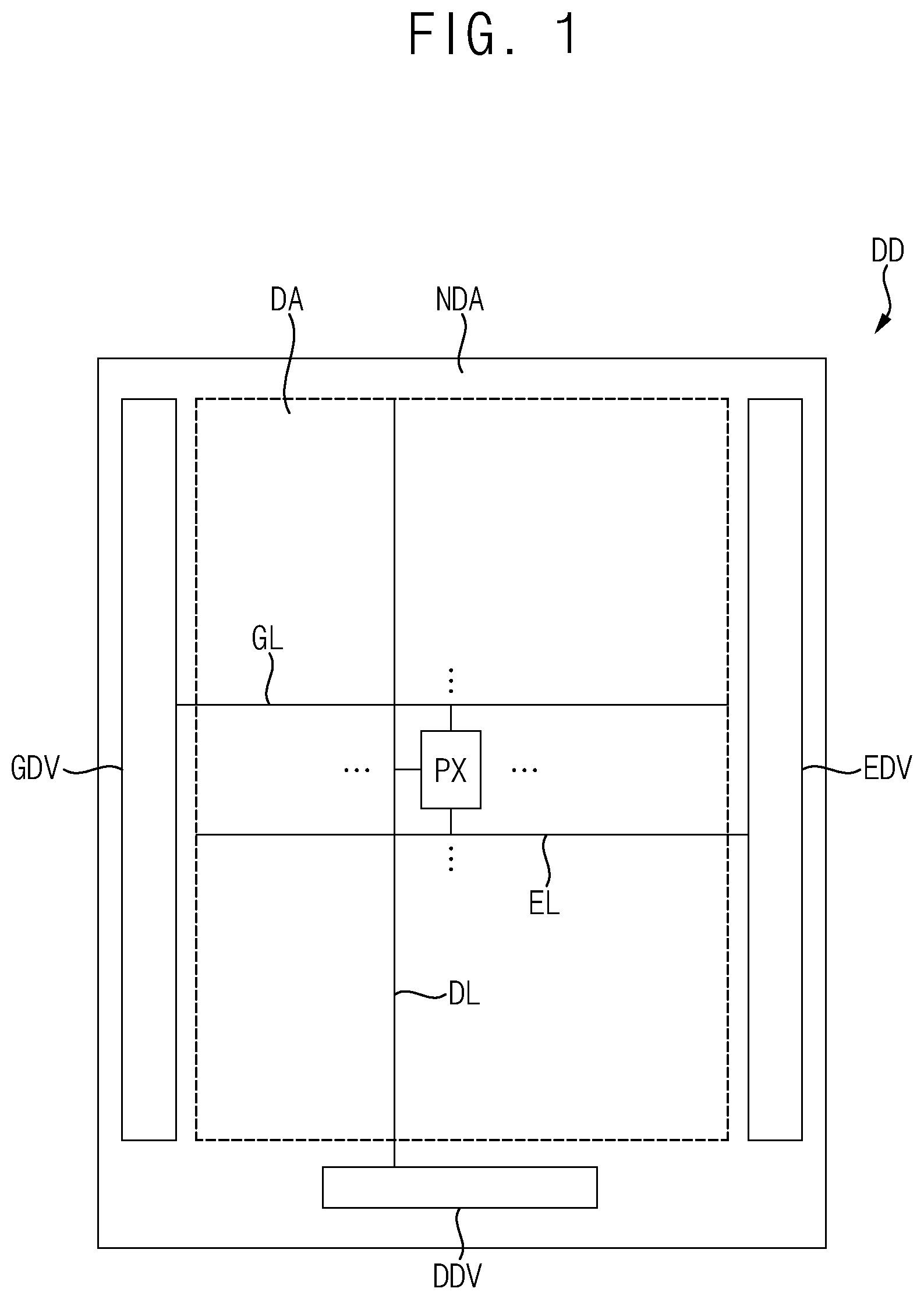
is a plan view illustrating a display device according to embodiments of the present disclosure. is a block diagram illustrating the display device of .
Referring to , a display device DD may include a display area DA and a non-display area NDA.
The display area DA may be an area that displays an image. A plurality of pixels PX may be disposed in the display area DA. As the pixels PX emit light, the display area DA may display an image.
The non-display area NDA may be an area that does not display an image. The non-display area NDA may surround at least a portion of the display area DA. For example, the non-display area NDA may entirely surround the display area DA. A driver that provides a signal or a voltage to the pixels PX may be disposed in the non-display area NDA. For example, the driver may include a gate driver GDV, a light emitting driver EDV, a data driver DDV, and a controller CON.
Each of the pixels PX may be electrically connected to the gate driver GDV, the light emitting driver EDV, and the data driver DDV. Specifically, each of the pixels PX may be connected to the gate driver GDV through a gate line GL, may be connected to the light emitting driver EDV through a light emitting line EL, and may be connected to the data driver DDV through a data line DL. Accordingly, each of the pixels PX may receive a gate signal GS, a light emitting signal EM, and a data voltage DATA.
The gate driver GDV may receive a gate control signal GCTRL from the controller CON. The gate driver GDV may generate the gate signal GS based on the gate control signal GCTRL. The gate signal GS may be provided to each of the pixels PX through the gate line GL.
The light emitting driver EDV may receive a light emitting control signal ECTRL from the controller CON. The light emitting driver EDV may generate the light emitting signal EM based on the light emitting control signal ECTRL. The light emitting signal EM may be provided to each of the pixels PX through the light emitting line EL.
The data driver DDV may receive a data control signal DCTRL and output image data ODAT from the controller CON. The data driver DDV may generate the data voltage DATA based on the data control signal DCTRL and the output image data ODAT. The data voltage DATA may be provided to each of the pixels PX through the data line DL.
The controller CON may receive a control signal CTRL and input image data IDAT from an external device (e.g., GPU). The controller CON may generate the gate control signal GCTRL, the light emitting control signal ECTRL, the data control signal DCTRL, and the output image data ODAT based on the control signal CTRL and the input image data IDAT. The controller CON may control the gate driver GDV, the light emitting driver EDV, and the data driver DDV.
In , the gate driver GDV is illustrated as being disposed on a first side of the display device DD, and the light emitting driver EDV is illustrated as being disposed on a second side of the display device DD, but the present disclosure is not limited thereto. In another embodiment, the gate driver GDV and the light emitting driver EDV may be disposed together on the first side or the second side of the display device DD. In still another embodiment, the gate driver GDV and the light emitting driver EDV may be integrally formed.
is a block diagram illustrating a driver included in the display device of .
Referring to , the display device DD may include a driver DV. In an embodiment, the driver DV may be the gate driver GDV or the light emitting driver EDV.
The driver DV may include a plurality of stages STG 1 , STG 2 , STG 3 , STG 4 , etc. The driver DV may be implemented in a form of a shift register in which the stages STG 1 , STG 2 , STG 3 , STG 4 , etc. sequentially output signals OUT 1 , OUT 2 , OUT 3 , OUT 4 , etc.
The stages STG 1 , STG 2 , STG 3 , STG 4 , etc. may sequentially output the output signals OUT 1 , OUT 2 , OUT 3 , OUT 4 , etc. based on a start signal FLM, a clock signal CLK, and an inverted clock signal CLKB. In addition, the first stage STG 1 may receive the start signal FLM as an input signal, and each of subsequent stages STG 2 , STG 3 , STG 4 , etc. may receive an output signal of a previous stage as an input signal. For example, the second stage STG 2 may receive a first output signal OUT 1 of the first stage STG 1 as an input signal, the third stage STG 3 may receive a second output signal OUT 2 of the second stage STG 2 as an input signal, and the fourth stage STG 4 may receive a third output signal OUT 3 of the third stage STG 3 as an input signal.
is a block diagram illustrating a stage of the driver of . is a circuit diagram illustrating a stage of a driver according to an embodiment of the present disclosure. is a graph illustrating a change in a threshold voltage of a transistor according to a voltage applied to a lower gate terminal of the transistor.
Referring to , 4 , 5 , and 6 , a stage 100 may include an input circuit INC and inverters INV 1 and INV 2 . In addition, the stage 100 may include a first transistor T 1 , a second transistor T 2 , a third transistor T 3 , a fourth transistor T 4 , a fifth transistor T 5 , a sixth transistor T 6 , a seventh transistor T 7 , and a storage capacitor CST.
The input circuit INC may transmit an input signal SIN to a first node N 1 . Specifically, the input circuit INC may transmit the input signal SIN to the first node N 1 in response to at least one of the clock signal CLK and the inverted clock signal CLKB. In an embodiment, the input circuit INC of the first stage STG 1 of the driver DV may receive the start signal FLM as the input signal SIN, and each of the subsequent stages STG 2 , STG 3 , STG 4 , etc. may receive an output signal OUT of the previous stage as the input signal SIN.
The input circuit INC may include the first transistor T 1 and the fifth transistor T 5 . In an embodiment, the first transistor T 1 and the fifth transistor T 5 may be connected in parallel.
In an embodiment, the first transistor T 1 may be a PMOS transistor, and the fifth transistor T 5 may be an NMOS transistor. That is, the input circuit INC may be implemented as a CMOS transmission gate including the first transistor T 1 and the fifth transistor T 5 .
The first transistor T 1 may include a gate terminal G 1 , a first terminal, and a second terminal. The gate terminal G 1 of the first transistor T 1 may receive the inverted clock signal CLKB. The first terminal of the first transistor T 1 may receive the input signal SIN. The second terminal of the first transistor T 1 may be connected to the first node N 1 . The first transistor T 1 may transmit the input signal SIN to the first node N 1 in response to the inverted clock signal CLKB.
The fifth transistor T 5 may include an upper gate terminal G 51 , a lower gate terminal G 52 , a first terminal, a second terminal, and a semiconductor material SC 1 . The upper gate terminal G 51 of the fifth transistor T 5 may receive the clock signal CLK. The lower gate terminal G 52 of the fifth transistor T 5 may be electrically connected to the upper gate terminal G 51 . The first terminal of the fifth transistor T 5 may receive the input signal SIN. The second terminal of the fifth transistor T 5 may be connected to the first node N 1 . The fifth transistor T 5 may transmit the input signal SIN to the first node N 1 in response to the clock signal CLK.
In an embodiment, the semiconductor material SC 1 may be connected to the upper gate terminal G 51 and the lower gate terminal G 52 , and may function as a Schottky diode. In this case, each of a work function of the upper gate terminal G 51 and a work function of the lower gate terminal G 52 may be greater than a work function of the semiconductor material SC 1 . That is, in the fifth transistor T 5 , the upper gate terminal G 51 and the lower gate terminal G 52 may be electrically connected through the semiconductor material SC 1 , and the semiconductor material SC 1 may make Schottky contact with the upper gate terminal G 51 and the lower gate terminal G 52 .
When an upper gate terminal and a lower gate terminal of a transistor are electrically connected to a Schottky diode, a depletion region may be formed. In the depletion region, as a voltage VLG applied to the lower gate terminal decreases, a threshold voltage VTH of the transistor may increase (see ).
Since the upper gate terminal G 51 and the lower gate terminal G 52 are connected to the semiconductor material SC 1 , a voltage different from a voltage applied to the upper gate terminal G 51 may be applied to the lower gate terminal G 52 , and a threshold voltage of the fifth transistor T 5 may be adjusted. In an embodiment, a voltage lower than the voltage applied to the upper gate terminal G 51 may be applied to the lower gate terminal G 52 , and the threshold voltage of the fifth transistor T 5 may increase.
The stage 100 may include an inverter chain including an even number of inverters INV 1 and INV 2 connected in series. In an embodiment, the stage 100 may include a first inverter INV 1 and a second inverter INV 2 connected in series.
The first inverter INV 1 may include an input terminal connected to the first node N 1 and an output terminal connected to the second node N 2 . The first inverter INV 1 may invert a voltage of the first node N 1 . In addition, the second inverter INV 2 may include an input terminal connected to the second node N 2 and an output terminal connected to an output node NO. The second inverter INV 2 may invert a voltage of the second node N 2 and generate an output signal OUT. Accordingly, the output signal OUT having a voltage corresponding to the voltage of the first node N 1 may be output from the output node NO.
The first inverter INV 1 may include the second transistor T 2 and the sixth transistor T 6 . In an embodiment, the second transistor T 2 and the sixth transistor T 6 may be connected in series.
In an embodiment, the second transistor T 2 may be a PMOS transistor, and the sixth transistor T 6 may be an NMOS transistor. That is, the first inverter INV 1 may be implemented as a CMOS inverter including the second transistor T 2 and the sixth transistor T 6 .
The second transistor T 2 may include a gate terminal G 2 , a first terminal, and a second terminal. The gate terminal G 2 of the second transistor T 2 may be connected to the first node N 1 . The first terminal of the second transistor T 2 may receive a high gate voltage VGH. The second terminal of the second transistor T 2 may be connected to the second node N 2 . When the voltage of the first node N 1 is at a low level, the second transistor T 2 may transmit the high gate voltage VGH to the second node N 2 in response to the voltage of the first node N 1 .
The sixth transistor T 6 may include an upper gate terminal G 61 , a lower gate terminal G 62 , a first terminal, a second terminal, and a semiconductor material SC 2 . The upper gate terminal G 61 of the sixth transistor T 6 may be connected to the first node N 1 . The lower gate terminal G 62 of the sixth transistor T 6 may be electrically connected to the upper gate terminal G 61 . The first terminal of the sixth transistor T 6 may receive a low gate voltage VGL. The second terminal of the sixth transistor T 6 may be connected to the second node N 2 . When the voltage of the first node N 1 is at a high level, the sixth transistor T 6 may transmit the low gate voltage VGL to the second node N 2 in response to the voltage of the first node N 1 .
In an embodiment, the semiconductor material SC 1 may be connected to the upper gate terminal G 61 and the lower gate terminal G 62 , and may function as a Schottky diode. In this case, each of a work function of the upper gate terminal G 61 and a work function of the lower gate terminal G 62 may be greater than a work function of the semiconductor material SC 2 . That is, in the sixth transistor T 6 , the upper gate terminal G 61 and the lower gate terminal G 62 may be electrically connected through the semiconductor material SC 2 , and the semiconductor material SC 2 may make Schottky contact with the upper gate terminal G 61 and the lower gate terminal G 62 .
Accordingly, a voltage different from a voltage applied to the upper gate terminal G 61 may be applied to the lower gate terminal G 62 , and a threshold voltage of the sixth transistor T 6 may be adjusted. In an embodiment, a voltage lower than the voltage applied to the upper gate terminal G 61 may be applied to the lower gate terminal G 62 , and the threshold voltage of the sixth transistor T 6 may increase.
The second inverter INV 2 may include the third transistor T 3 and the seventh transistor T 7 . In an embodiment, the third transistor T 3 and the seventh transistor T 7 may be connected in series.
In an embodiment, the third transistor T 3 may be a PMOS transistor, and the seventh transistor T 7 may be an NMOS transistor. That is, the second inverter INV 2 may be implemented as a CMOS inverter including the third transistor T 3 and the seventh transistor T 7 .
The third transistor T 3 may include a gate terminal G 3 , a first terminal, and a second terminal. The gate terminal G 3 of the third transistor T 3 may be connected to the second node N 2 . The first terminal of the third transistor T 3 may receive the high gate voltage VGH. The second terminal of the third transistor T 3 may be connected to the output node NO. When a voltage of the second node N 2 is at a low level, the third transistor T 3 may transmit the high gate voltage VGH to the output node NO in response to the voltage of the second node N 2 .
The seventh transistor T 7 may include an upper gate terminal G 71 , a lower gate terminal G 72 , a first terminal, a second terminal, and a semiconductor material SC 3 . The upper gate terminal G 71 of the seventh transistor T 7 may be connected to the second node N 2 . The lower gate terminal G 72 of the seventh transistor T 7 may be electrically connected to the upper gate terminal G 71 . The first terminal of the seventh transistor T 7 may receive the low gate voltage VGL. The second terminal of the seventh transistor T 7 may be connected to the output node NO. When the voltage of the second node N 2 is at a high level, the seventh transistor T 7 may transmit the low gate voltage VGL to the output node NO in response to the voltage of the second node N 2 .
In an embodiment, the semiconductor material SC 3 may be connected to the upper gate terminal G 71 and the lower gate terminal G 72 , and may function as a Schottky diode. In this case, each of a work function of the upper gate terminal G 71 and a work function of the lower gate terminal G 72 may be greater than a work function of the semiconductor material SC 3 . That is, in the seventh transistor T 7 , the upper gate terminal G 71 and the lower gate terminal G 72 may be electrically connected through the semiconductor material SC 3 , and the semiconductor material SC 3 may make Schottky contact with the upper gate terminal G 71 and the lower gate terminal G 72 .
Accordingly, a voltage different from a voltage applied to the upper gate terminal G 71 may be applied to the lower gate terminal G 72 , and a threshold voltage of the seventh transistor T 7 may be adjusted. In an embodiment, a voltage lower than the voltage applied to the upper gate terminal G 71 may be applied to the lower gate terminal G 72 , and the threshold voltage of the seventh transistor T 7 may increase.
The fourth transistor T 4 may include a gate terminal G 4 , a first terminal, and a second terminal. The gate terminal G 4 of the fourth transistor T 4 may receive a global reset signal ESR. The first terminal of the fourth transistor T 4 may receive the high gate voltage VGH. The second terminal of the fourth transistor T 4 may be connected to the first node N 1 . When a power-on sequence of a display device is performed, the fourth transistor T 4 may transmit the high gate voltage VGH to the first node N 1 in response to the global reset signal ESR. Accordingly, the fourth transistor T 4 may stabilize the voltage of the first node N 1 during the power-on sequence.
In , the fourth transistor T 4 is illustrated as receiving the high gate voltage VGH, but the present disclosure is not limited thereto. In another embodiment, the first terminal of the fourth transistor T 4 may receive the low gate voltage VGL. In this case, the fourth transistor T 4 may transmit the low gate voltage VGL to the first node N 1 in response to the global reset signal ESR during the power-on sequence.
The storage capacitor CST may include a first terminal and a second terminal. The first terminal of the storage capacitor CST may receive the high gate voltage VGH. The second terminal of the storage capacitor CST may be connected to the first node N 1 . The storage capacitor CST may maintain the voltage of the first node N 1 while the first transistor T 1 and the fifth transistor T 5 of the input circuit INC are turned off.
In , the storage capacitor CST is illustrated as receiving the high gate voltage VGH, but the present disclosure is not limited thereto. In another embodiment, the first terminal of the storage capacitor CST may receive the low gate voltage VGL.
is a cross-sectional view illustrating an example of transistors included in the stage of . is an enlarged plan view of area A of .
Referring to , 7 , and 8 , the stage 100 may include a substrate SUB, a buffer layer BFR, a first active pattern AP 1 , a first gate insulating layer GI 1 , a first gate electrode GE 1 , a second gate insulating layer GI 2 , a second gate electrode GE 2 , a first interlayer insulating layer ILD 1 , a second active pattern AP 2 , a semiconductor pattern SP, a third gate insulating layer GI 3 , a third gate electrode GE 3 , a fourth gate electrode GE 4 , a second interlayer insulating layer ILD 2 , a first source electrode SE 1 , a first drain electrode DE 1 , a second source electrode SE 2 , a second drain electrode DE 2 , and a via insulating layer VIA.
The substrate SUB may include a transparent or opaque material. The substrate SUB may include glass, quartz, plastic, or the like. These may be used alone or in combination with each other.
The buffer layer BFR may be disposed on the substrate SUB. The buffer layer BFR may prevent metal atoms or impurities from being diffused from the substrate SUB to transistors. In addition, the buffer layer BFR may improve a flatness of a surface of the substrate SUB when the surface of the substrate SUB is not uniform. The buffer layer BFR may include an inorganic material such as silicon oxide (SiO x ), silicon nitride (SiN x ), silicon carbide (SiC x ), silicon oxynitride (SiO x N y ), silicon oxycarbide (SiO x C y ), or the like. These may be used alone or in combination with each other.
The first active pattern AP 1 may be disposed on the buffer layer BFR. The first active pattern AP 1 may include a source area SA 1 , a drain area DA 1 , and a channel area CA 1 positioned between the source area SA 1 and the drain area DA 1 . In an embodiment, the first active pattern AP 1 may include a silicon semiconductor material. Examples of the silicon semiconductor material may include amorphous silicon, polycrystalline silicon, or the like. These may be used alone or in combination with each other.
In an embodiment, the first active pattern AP 1 may include a P-type impurity. For example, the P-type impurity may include boron (B) ions. The P-type impurity may be doped into the source area SA 1 and the drain area DA 1 of the first active pattern AP 1 . For example, the first active pattern AP 1 may correspond to the first terminals and the second terminals of the first, second, third, and fourth transistors T 1 , T 2 , T 3 , and T 4 .
The first gate insulating layer GI 1 may be disposed on the buffer layer BFR, and may cover the first active pattern AP 1 . The first gate insulating layer GI 1 may include an inorganic material such as silicon oxide, silicon nitride, silicon carbide, silicon oxynitride, silicon oxy carbide, or the like. These may be used alone or in combination with each other.
The first gate electrode GE 1 may be disposed on the first gate insulating layer GI 1 . The first gate electrode GE 1 may overlap the channel area CA 1 of the first active pattern AP 1 . The first gate electrode GE 1 may include metal, alloy, conductive metal oxide, metal nitride, or the like. Examples of the metal may include silver (Ag), molybdenum (Mo), aluminum (Al), tungsten (W), copper (Cu), nickel (Ni), chromium (Cr), titanium (Ti), tantalum (Ta), platinum (Pt), scandium (Sc), or the like. Examples of the conductive metal oxide may include indium tin oxide, indium zinc oxide, or the like. Examples of the metal nitride may include aluminum nitride (AlN x ), tungsten nitride (WN x ), chromium nitride (CrN x ), or the like. These may be used alone or in combination with each other. For example, the first gate electrode GE 1 may correspond to the gate terminals G 1 , G 2 , G 3 , and G 4 of the first, second, third, and fourth transistors T 1 , T 2 , T 3 , and T 4 .
The second gate insulating layer GI 2 may be disposed on the first gate insulating layer GI 1 , and may cover the first gate electrode GE 1 . The second gate insulating layer GI 2 may include an inorganic material such as silicon oxide, silicon nitride, silicon carbide, silicon oxynitride, silicon oxycarbide, or the like. These may be used alone or in combination with each other.
The second gate electrode GE 2 may be disposed on the second gate insulating layer GI 2 . The second gate electrode GE 2 may include metal, alloy, conductive metal oxide, metal nitride, or the like. Examples of the metal may include silver, molybdenum, aluminum, tungsten, copper, nickel, chromium, titanium, tantalum, platinum, scandium, or the like. Examples of the conductive metal oxide may include indium tin oxide, indium zinc oxide, or the like. Examples of the metal nitride may include aluminum nitride, tungsten nitride, chromium nitride, or the like. These may be used alone or in combination with each other. For example, the second gate electrode GE 2 may correspond to the lower gate terminals G 52 , G 62 , and G 72 of the fifth, sixth, and seventh transistors T 5 , T 6 , and T 7 .
The first interlayer insulating layer ILD 1 may be disposed on the second gate insulating layer GI 2 , and may cover the second gate electrode GE 2 . The first interlayer insulating layer ILD 1 may include an inorganic material such as silicon oxide, silicon nitride, silicon carbide, silicon oxynitride, silicon oxycarbide, or the like. These may be used alone or in combination with each other.
The second active pattern AP 2 and the semiconductor pattern SP may be disposed on the first interlayer insulating layer ILD 1 . The second active pattern AP 2 and the semiconductor pattern SP may be disposed on a same layer. In an embodiment, the second active pattern AP 2 and the semiconductor pattern SP may be spaced apart from each other. The second active pattern AP 2 and the semiconductor pattern SP may include a same material, and may be disposed on a same layer. That is, the second active pattern AP 2 and the semiconductor pattern SP may be formed through a same process by using a same material.
Each of the second active pattern AP 2 and the semiconductor pattern SP may include a material different from a material of the first active pattern AP 1 . In an embodiment, each of the second active pattern AP 2 and the semiconductor pattern SP may include an oxide semiconductor material. Examples of the oxide semiconductor material may include indium gallium zinc oxide, indium tin zinc oxide, or the like. These may be used alone or in combination with each other.
The second active pattern AP 2 may include a source area SA 2 , a drain area DA 2 , and a channel area CA 2 positioned between the source area SA 2 and the drain area DA 2 . In an embodiment, the second active pattern AP 2 may include an N-type impurity. For example, the N-type impurity may include phosphorus (P) ions. The N-type impurity may be doped into the source area SA 2 and the drain area DA 2 of the second active pattern AP 2 . For example, the second active pattern AP 2 may correspond to the first terminals and the second terminals of the fifth, sixth, and seventh transistors T 5 , T 6 , and T 7 .
The semiconductor pattern SP may be in contact with the second gate electrode GE 2 through a first contact hole CNT 1 penetrating a portion of the first interlayer insulating layer ILD 1 . In an embodiment, a work function of the second gate electrode GE 2 may be greater than a work function of the semiconductor pattern SP.
For example, the second gate electrode GE 2 may include copper, and the semiconductor pattern SP may include indium gallium zinc oxide. In this case, the work function of the second gate electrode GE 2 may be about 4.53 eV to about 5.10 eV, and the work function of the semiconductor pattern SP may be about 4.0 eV. For another example, the second gate electrode GE 2 may include at least one of aluminum and titanium, and the semiconductor pattern SP may include indium gallium zinc oxide. In this case, the work function of the second gate electrode GE 2 may be about 4.06 eV to about 4.33 eV. For still another example, the second gate electrode GE 2 may include molybdenum, and the semiconductor pattern SP may include indium gallium zinc oxide. In this case, the work function of the second gate electrode GE 2 may be about 4.53 eV to about 5.10 eV.
Accordingly, the semiconductor pattern SP and the second gate electrode GE 2 may be in Schottky contact through the first contact hole CNT 1 . For example, the semiconductor pattern SP may correspond to the semiconductor materials SC 1 , SC 2 , and SC 3 of the fifth, sixth, and seventh transistors T 5 , T 6 , and T 7 .
The third gate insulating layer GI 3 may be disposed on the first interlayer insulating layer ILD 1 , and may cover the second active pattern AP 2 and the semiconductor pattern SP. The third gate insulating layer GI 3 may include an inorganic material such as silicon oxide, silicon nitride, silicon carbide, silicon oxynitride, silicon oxycarbide, or the like. These may be used alone or in combination with each other.
The third gate electrode GE 3 and the fourth gate electrode GE 4 may be disposed on the third gate insulating layer GI 3 . The third gate electrode GE 3 and the fourth gate electrode GE 4 may include a same material, and may be disposed on a same layer. That is, the third gate electrode GE 3 and the fourth gate electrode GE 4 may be formed through a same process by using a same material.
The third gate electrode GE 3 and the fourth gate electrode GE 4 may include metal, alloy, conductive metal oxide, metal nitride, or the like. Examples of the metal may include silver, molybdenum, aluminum, tungsten, copper, nickel, chromium, titanium, tantalum, platinum, scandium, or the like. Examples of the conductive metal oxide may include indium tin oxide, indium zinc oxide, or the like. Examples of the metal nitride may include aluminum nitride, tungsten nitride, chromium nitride, or the like. These may be used alone or in combination with each other.
The third gate electrode GE 3 may overlap the channel area CA 2 of the second active pattern AP 2 . For example, the third gate electrode GE 3 may correspond to the upper gate terminals G 51 , G 61 , and G 71 of the fifth, sixth, and seventh transistors T 5 , T 6 , and T 7 .
The fourth gate electrode GE 4 may be in contact with the semiconductor pattern SP through a second contact hole CNT 2 penetrating a portion of the third gate insulating layer GI 3 . Accordingly, the second gate electrode GE 2 and the fourth gate electrode GE 4 may be electrically connected. In an embodiment, a work function of the fourth gate electrode GE 4 may be greater than the work function of the semiconductor pattern SP.
For example, the fourth gate electrode GE 4 may include copper, and the semiconductor pattern SP may include indium gallium zinc oxide. For another example, the fourth gate electrode GE 4 may include at least one of aluminum and titanium, and the semiconductor pattern SP may include indium gallium zinc oxide. For still another example, the fourth gate electrode GE 4 may include molybdenum, and the semiconductor pattern SP may include indium gallium zinc oxide.
Accordingly, the fourth gate electrode GE 4 and the semiconductor pattern SP may be in Schottky contact through the second contact hole CNT 2 . For example, the fourth gate electrode GE 4 may correspond to the upper gate terminals G 51 , G 61 , and G 71 of the fifth, sixth, and seventh transistors T 5 , T 6 , and T 7 .
The second interlayer insulating layer ILD 2 may be disposed on the third gate insulating layer GI 3 , and may cover the third gate electrode GE 3 and the fourth gate electrode GE 4 . The second interlayer insulating layer ILD 2 may include an inorganic material such as silicon oxide, silicon nitride, silicon carbide, silicon oxynitride, silicon oxycarbide, or the like. These may be used alone or in combination with each other.
The first source electrode SE 1 , the first drain electrode DE 1 , the second source electrode SE 2 , and the second drain electrode DE 2 may be disposed on the second interlayer insulating layer ILD 2 . The first source electrode SE 1 , the first drain electrode DE 1 , the second source electrode SE 2 , and the second drain electrode DE 2 may include a same material, and may be disposed on a same layer. That is, the first source electrode SE 1 , the first drain electrode DE 1 , the second source electrode SE 2 , and the second drain electrode DE 2 may be formed through a same process using a same material.
The first source electrode SE 1 , the first drain electrode DE 1 , the second source electrode SE 2 , and the second drain electrode DE 2 may include metal, alloy, conductive metal oxide, metal nitride, or the like. Examples of the metal may include silver, molybdenum, aluminum, tungsten, copper, nickel, chromium, titanium, tantalum, platinum, scandium, or the like. Examples of the conductive metal oxide may include indium tin oxide, indium zinc oxide, or the like. Examples of the metal nitride may include aluminum nitride, tungsten nitride, chromium nitride, or the like. These may be used alone or in combination with each other.
The first source electrode SE 1 may be in contact with the source area SA 1 of the first active pattern AP 1 through a contact hole penetrating portions of the first, second, and third gate insulating layers GI 1 , GI 2 , and GI 3 and the first and second interlayer insulating layers ILD 1 and ILD 2 . The first drain electrode DE 1 may be in contact with the drain area DA 1 of the first active pattern AP 1 through a contact hole penetrating portions of the first, second, and third gate insulating layers GI 1 , GI 2 , and GI 3 and the first and second interlayer insulating layers ILD 1 and ILD 2 .
In addition, the second source electrode SE 2 may be in contact with the source area SA 2 of the second active pattern AP 2 through a contact hole penetrating portions of the third gate insulating layer GI 3 and the second interlayer insulating layer ILD 2 . The second drain electrode DE 2 may be in contact with the drain area DA 2 of the second active pattern AP 2 through a contact hole penetrating portions of the third gate insulating layer GI 3 and the second interlayer insulating layer ILD 2 .
Accordingly, the first, second, third, and fourth transistors T 1 , T 2 , T 3 and T 4 including the first active pattern AP 1 , the first gate electrode GE 1 , the first source electrode SE 1 , and the first drain electrode DE 1 may be disposed on the substrate SUB.
In addition, the fifth, sixth, and seventh transistors T 5 , T 6 , and T 7 including the second gate electrode GE 2 , the second active pattern AP 2 , the semiconductor pattern SP, the third gate electrode GE 3 , the fourth gate electrode GE 4 , the second source electrode SE 2 , and the second drain electrode DE 2 may be disposed on the substrate SUB.
The via insulating layer VIA may be disposed on the second interlayer insulating layer ILD 2 , and may cover the first source electrode SE 1 , the first drain electrode DE 1 , the second source electrode SE 2 , and the second drain electrode DE 2 . The via insulating layer VIA may include an organic material such as phenol resin, acrylic resin, polyimide resin, polyamide resin, siloxane resin, epoxy resin, or the like. These may be used alone or in combination with each other.
is a cross-sectional view illustrating another example of transistors included in the stage of .
Hereinafter, descriptions overlapping the stage 100 described with reference to will be omitted or simplified.
Referring to , the stage 100 may include a substrate SUB, a buffer layer BFR, a first active pattern AP 1 , the first gate insulating layer GI 1 , a first gate electrode GE 1 , a second gate insulating layer GI 2 , a semiconductor pattern SP, a first interlayer insulating layer ILD 1 , a second active pattern AP 2 , a third gate insulating layer GI 3 , a second gate electrode GE 2 , a third gate electrode GE 3 , a second interlayer insulating layer ILD 2 , a first source electrode SE 1 , a first drain electrode DE 1 , a second source electrode SE 2 , a second drain electrode DE 2 , and a via insulating layer VIA.
The buffer layer BFR, the first active pattern AP 1 , the first gate insulating layer GI 1 , the first gate electrode GE 1 , and the second gate insulating layer GI 2 may be sequentially disposed on the substrate SUB.
The semiconductor pattern SP may be disposed on the second gate insulating layer GI 2 . In an embodiment, the semiconductor pattern SP may include an oxide semiconductor material. Examples of the oxide semiconductor material may include indium gallium zinc oxide, indium tin zinc oxide, or the like. These may be used alone or in combination with each other. For example, the semiconductor pattern SP may correspond to the lower gate terminals G 52 , G 62 , and G 72 and the semiconductor materials SC 1 , SC 2 , and SC 3 of the fifth, sixth, and seventh transistors T 5 , T 6 , and T 7 .
The first interlayer insulating layer ILD 1 , the second active pattern AP 2 , and the third gate insulating layer GI 3 may be sequentially disposed on the second gate insulating layer GI 2 .
The second gate electrode GE 2 and the third gate electrode GE 3 may be disposed on the third gate insulating layer GI 3 . The second gate electrode GE 2 and the third gate electrode GE 3 may be formed through a same process using a same material. The second gate electrode GE 2 and the third gate electrode GE 3 may include metal, alloy, conductive metal oxide, metal nitride, or the like.
The second gate electrode GE 2 may overlap a channel area CA 2 of the second active pattern AP 2 . For example, the second gate electrode GE 2 may correspond to the upper gate terminals G 51 , G 61 , and G 71 of the fifth, sixth, and seventh transistors T 5 , T 6 , and T 7 .
The third gate electrode GE 3 may be in contact with the semiconductor pattern SP through a contact hole CNT penetrating portions of the first interlayer insulating layer ILD 1 and the third gate insulating layer GI 3 . Accordingly, the semiconductor pattern SP and the third gate electrode GE 3 may be electrically connected. In an embodiment, a work function of the third gate electrode GE 3 may be greater than a work function of the semiconductor pattern SP.
For example, the third gate electrode GE 3 may include copper, and the semiconductor pattern SP may include indium gallium zinc oxide. For another example, the third gate electrode GE 3 may include at least one of aluminum and titanium, and the semiconductor pattern SP may include indium gallium zinc oxide. For still another example, the third gate electrode GE 3 may include molybdenum, and the semiconductor pattern SP may include indium gallium zinc oxide.
Accordingly, the semiconductor pattern SP and the third gate electrode GE 3 may be in Schottky contact through the contact hole CNT. For example, the third gate electrode GE 3 may correspond to the upper gate terminals G 51 , G 61 , and G 71 of the fifth, sixth, and seventh transistors T 5 , T 6 , and T 7 .
The second interlayer insulating layer ILD 2 , the first source electrode SE 1 , the first drain electrode DE 1 , the second source electrode SE 2 , the second drain electrode DE 2 , and the via insulating layer VIA may be sequentially disposed on the third gate insulating layer GI 3 .
Accordingly, the fifth, sixth, and seventh transistors T 5 , T 6 , and T 7 including the semiconductor pattern SP, the second active pattern AP 2 , the second gate electrode GE 2 , the third gate electrode GE 3 , the second source electrode SE 2 , and the second drain electrode DE 2 may be disposed on the substrate SUB.
The stage 100 of the driver DV according to an embodiment of the present disclosure may include the first, second, third, and fourth transistors T 1 , T 2 , T 3 , and T 4 including a silicon semiconductor and the fifth, sixth, and seventh transistors T 5 , T 6 , and T 7 including an oxide semiconductor. In this case, in the fifth, sixth, and seventh transistors T 5 , T 6 , and T 7 , the upper gate terminals G 51 , G 61 , and G 71 and the lower gate terminals G 52 , G 62 , and G 72 may be electrically connected through the semiconductor materials SC 1 , SC 2 , and SC 3 . Since the work function of the upper gate terminals G 51 , G 61 , and G 71 and the work function of the lower gate terminals G 52 , G 62 , and G 72 are greater than the work function of the semiconductor materials SC 1 , SC 2 , and SC 3 , the voltage applied to each of the lower gate terminals G 52 , G 62 , and G 72 may be lowered, and the threshold voltage of each of the fifth, sixth, and seventh transistors T 5 , T 6 , and T 7 may increase.
In addition, since the fifth, sixth, and seventh transistors T 5 , T 6 , and T 7 have a double gate structure including the upper gate terminals G 51 , G 61 , and G 71 and the lower gate terminals G 52 , G 62 , and G 72 , output current may increase. Accordingly, the driver DV may require a relatively small number of buffer transistors, and thus a dead space of the display device DD may be reduced.
In addition, each of the first, second, third, and fourth transistors T 1 , T 2 , T 3 , and T 4 may be a PMOS transistor, and each of the fifth, sixth, and seventh transistors T 5 , T 6 , and T 7 may be an NMOS transistor. As the stage 100 of the driver DV includes a CMOS circuit, power consumption of the driver DV and the display device DD may be reduced.
is a circuit diagram illustrating a stage of a driver according to another embodiment of the present disclosure.
Hereinafter, descriptions overlapping the stage 100 described with reference to will be omitted or simplified.
Referring to , a stage 200 may include an input circuit INC, a first inverter INV 1 , and a second inverter INV 2 . In addition, the stage 200 may include a first transistor T 1 , a second transistor T 2 , a third transistor T 3 , a fourth transistor T 4 , a fifth transistor T 5 , a sixth transistor T 6 , a seventh transistor T 7 , and a storage capacitor CST.
The input circuit INC may transmit an input signal SIN to a first node N 1 in response to at least one of a clock signal CLK and an inverted clock signal CLKB.
The input circuit INC may include the first transistor T 1 and the fifth transistor T 5 connected in parallel. In an embodiment, the first transistor T 1 may be a PMOS transistor, and the fifth transistor T 5 may be an NMOS transistor.
The first transistor T 1 may include a gate terminal G 1 that receives the inverted clock signal CLKB, a first terminal that receives the input signal SIN, and a second terminal connected to the first node N 1 .
The fifth transistor T 5 may include an upper gate terminal G 51 that receives the clock signal CLK, a lower gate terminal G 52 electrically connected to the upper gate terminal G 51 , a first terminal that receives the input signal SIN, a second terminal connected to the first node N 1 , and a semiconductor material R 1 .
In an embodiment, the semiconductor material R 1 may be connected to the upper gate terminal G 51 and the lower gate terminal G 52 , and may function as a resistor. That is, in the fifth transistor T 5 , the upper gate terminal G 51 and the lower gate terminal G 52 may be electrically connected through the semiconductor material R 1 , and the semiconductor material R 1 may make ohmic contact with the upper gate terminal G 51 and the lower gate terminal G 52 .
Accordingly, a voltage different from a voltage applied to the upper gate terminal G 51 may be applied to the lower gate terminal G 52 , and a threshold voltage of the fifth transistor T 5 may be adjusted. In an embodiment, a voltage lower than the voltage applied to the upper gate terminal G 51 may be applied to the lower gate terminal G 52 , and the threshold voltage of the fifth transistor T 5 may increase.
The first inverter INV 1 may invert a voltage of the first node N 1 . The first inverter INV 1 may include the second transistor T 2 and the sixth transistor T 6 connected in series. In an embodiment, the second transistor T 2 may be a PMOS transistor, and the sixth transistor T 6 may be an NMOS transistor.
The second transistor T 2 may include a gate terminal G 2 connected to the first node N 1 , a first terminal that receives a high gate voltage VGH, and a second terminal connected to a second node N 2 .
The sixth transistor T 6 may include an upper gate terminal G 61 connected to the first node N 1 , a lower gate terminal G 62 electrically connected to the upper gate terminal G 61 , a first terminal that receives a low gate voltage VGL, a second terminal connected to the second node N 2 , and a semiconductor material R 2 .
In an embodiment, the semiconductor material R 2 may be connected to the upper gate terminal G 61 and the lower gate terminal G 62 , and may function as a resistor. That is, in the sixth transistor T 6 , the upper gate terminal G 61 and the lower gate terminal G 62 may be electrically connected through the semiconductor material R 2 , and the semiconductor material R 2 may make ohmic contact with the upper gate terminal G 61 and the lower gate terminal G 62 .
Accordingly, a voltage different from a voltage applied to the upper gate terminal G 61 may be applied to the lower gate terminal G 62 , and a threshold voltage of the sixth transistor T 6 may be adjusted. In an embodiment, a voltage lower than the voltage applied to the upper gate terminal G 61 may be applied to the lower gate terminal G 62 , and the threshold voltage of the sixth transistor T 6 may increase.
The second inverter INV 2 may invert a voltage of the second node N 2 and generate an output signal OUT. The second inverter INV 2 may include the third transistor T 3 and the seventh transistor T 7 connected in series. In an embodiment, the third transistor T 3 may be a PMOS transistor, and the seventh transistor T 7 may be an NMOS transistor.
The third transistor T 3 may include a gate terminal G 3 connected to the second node N 2 , a first terminal that receives the high gate voltage VGH, and a second terminal connected to an output node NO.
The seventh transistor T 7 may include an upper gate terminal G 71 connected to the second node N 2 , a lower gate terminal G 72 electrically connected to the upper gate terminal G 71 , a first terminal that receives the low gate voltage VGL, a second terminal connected to the output node NO, and a semiconductor material R 3 .
In an embodiment, the semiconductor material R 3 may be connected to the upper gate terminal G 71 and the lower gate terminal G 72 , and may function as a resistor. That is, in the seventh transistor T 7 , the upper gate terminal G 71 and the lower gate terminal G 72 may be electrically connected through the semiconductor material R 3 , and the semiconductor material R 3 may make ohmic contact with the upper gate terminal G 71 and the lower gate terminal G 72 .
Accordingly, a voltage different from a voltage applied to the upper gate terminal G 71 may be applied to the lower gate terminal G 72 , and a threshold voltage of the seventh transistor T 7 may be adjusted. In an embodiment, a voltage lower than the voltage applied to the upper gate terminal G 71 may be applied to the lower gate terminal G 72 , and the threshold voltage of the seventh transistor T 7 may increase.
The fourth transistor T 4 may include a gate terminal G 4 that receives a global reset signal ESR, a first terminal that receives the high gate voltage VGH, and a second terminal connected to the first node N 1 .
The storage capacitor CST may include a first terminal that receives the high gate voltage VGH and a second terminal connected to the first node N 1 .
is a cross-sectional view illustrating an example of transistors included in the stage of .
Hereinafter, descriptions overlapping the stage 100 described with reference to will be omitted or simplified.
Referring to , the stage 200 may include a substrate SUB, a buffer layer BFR, a first active pattern AP 1 , a first gate insulating layer GI 1 , a first gate electrode GE 1 , a second gate insulating layer GI 2 , a second gate electrode GE 2 , a first interlayer insulating layer ILD 1 , a second active pattern AP 2 , a semiconductor pattern SP, a third gate insulating layer GI 3 , a third gate electrode GE 3 , a fourth gate electrode GE 4 , a second interlayer insulating layer ILD 2 , a first source electrode SE 1 , a first drain electrode DE 1 , a second source electrode SE 2 , a second drain electrode DE 2 , a connection electrode CE, and a via insulating layer VIA.
The buffer layer BFR, the first active pattern AP 1 , the first gate insulating layer GI 1 , the first gate electrode GE 1 , the second gate insulating layer GI 2 , the second gate electrode GE 2 , and the first interlayer insulating layer ILD 1 may be sequentially disposed on the substrate SUB.
The second active pattern AP 2 and the semiconductor pattern SP may be disposed on the first interlayer insulating layer ILD 1 . The second active pattern AP 2 and the semiconductor pattern SP may be disposed on a same layer. In an embodiment, the second active pattern AP 2 and the semiconductor pattern SP may be spaced apart from each other. The second active pattern AP 2 and the semiconductor pattern SP may be formed by a same process using a same material. In an embodiment, each of the second active pattern AP 2 and the semiconductor pattern SP may include an oxide semiconductor material.
In an embodiment, the semiconductor pattern SP may include an N-type impurity. That is, the N-type impurity may be doped into a source area SA 2 of the second active pattern AP 2 , a drain area DA 2 of the second active pattern AP 2 , and the semiconductor pattern SP.
The semiconductor pattern SP may be in contact with the second gate electrode GE 2 through a contact hole CNT penetrating a portion of the first interlayer insulating layer ILD 1 . As the N-type impurity is doped into the semiconductor pattern SP, the semiconductor pattern SP and the second gate electrode GE 2 may be in ohmic contact through the contact hole CNT. For example, the semiconductor pattern SP may correspond to the semiconductor materials R 1 , R 2 , and R 3 of the fifth, sixth, and seventh transistors T 5 , T 6 , and T 7 .
The third gate insulating layer GI 3 , the third gate electrode GE 3 , and the fourth gate electrode GE 4 may be sequentially disposed on the first interlayer insulating layer ILD 1 .
The third gate electrode GE 3 and the fourth gate electrode GE 4 may be formed by a same process using a same material. The third gate electrode GE 3 and the fourth gate electrode GE 4 may include metal, alloy, conductive metal oxide, metal nitride, or the like.
The fourth gate electrode GE 4 may be electrically connected to the second gate electrode GE 2 . In an embodiment, the fourth gate electrode GE 4 may not overlap the semiconductor pattern SP in a plan view. In other words, the fourth gate electrode GE 4 may be spaced apart from the semiconductor pattern SP in a plan view so that the semiconductor pattern SP may be doped with the N-type impurity. For example, the fourth gate electrode GE 4 may correspond to the upper gate terminals G 51 , G 61 , and G 71 of the fifth, sixth, and seventh transistors T 5 , T 6 , and T 7 .
The second interlayer insulating layer ILD 2 , the first source electrode SE 1 , the first drain electrode DE 1 , the second source electrode SE 2 , the second drain electrode DE 2 , and the connection electrode CE may be sequentially disposed on the third gate insulating layer GI 3 .
The first source electrode SE 1 , the first drain electrode DE 1 , the second source electrode SE 2 , the second drain electrode DE 2 , and the connection electrode CE may be formed through a same process using a same material. The first source electrode SE 1 , the first drain electrode DE 1 , the second source electrode SE 2 , the second drain electrode DE 2 , and the connection electrode CE may include metal, alloy, conductive metal oxide, metal nitride, or the like.
The connection electrode CE may be in contact with the semiconductor pattern SP through a contact hole penetrating portions of the third gate insulating layer GI 3 and the second interlayer insulating layer ILD 2 . In addition, the connection electrode CE may be in contact with the fourth gate electrode GE 4 through a contact hole penetrating a portion of the second interlayer insulating layer ILD 2 . Accordingly, the fourth gate electrode GE 4 may be electrically connected to the semiconductor pattern SP and the second gate electrode GE 2 , and the fourth gate electrode GE 4 and the semiconductor pattern SP may be in ohmic contact.
Accordingly, the fifth, sixth, and seventh transistors T 5 , T 6 , and T 7 including the second gate electrode GE 2 , the second active pattern AP 2 , the semiconductor pattern SP, the third gate electrode GE 3 , the fourth gate electrode GE 4 , the second source electrode SE 2 , the second drain electrode DE 2 , and the connection electrode CE may be disposed on the substrate SUB.
The via insulating layer VIA may be disposed on the second interlayer insulating layer ILD 2 , and may cover the first source electrode SE 1 , the first drain electrode DE 1 , the second source electrode SE 2 , the second drain electrode DE 2 , and the connection electrode CE.
The stage 200 of the driver DV according to an embodiment of the present disclosure may include the first, second, third, and fourth transistors T 1 , T 2 , T 3 , and T 4 including a silicon semiconductor and the fifth, sixth, and seventh transistors T 5 , T 6 , and T 7 including an oxide semiconductor. In this case, in the fifth, sixth, and seventh transistors T 5 , T 6 , and T 7 , the upper gate terminals G 51 , G 61 , and G 71 and the lower gate terminals G 52 , G 62 , and G 72 may be electrically connected through the semiconductor materials R 1 , R 2 , and R 3 . Accordingly, the voltage applied to each of the lower gate terminals G 52 , G 62 , and G 72 may be lowered, and the threshold voltage of each of the fifth, sixth, and seventh transistors T 5 , T 6 , and T 7 may increase.
In addition, since the fifth, sixth, and seventh transistors T 5 , T 6 , and T 7 have a double gate structure including the upper gate terminals G 51 , G 61 , and G 71 and the lower gate terminals G 52 , G 62 , and G 72 , output current may increase. Accordingly, the driver DV may require a relatively small number of buffer transistors, and thus a dead space of the display device DD may be reduced.
In addition, each of the first, second, third, and fourth transistors T 1 , T 2 , T 3 , and T 4 may be a PMOS transistor, and each of the fifth, sixth, and seventh transistors T 5 , T 6 , and T 7 may be an NMOS transistor. As the stage 200 of the driver DV includes a CMOS circuit, power consumption of the driver DV and the display device DD may be reduced.
The present disclosure can be applied to a manufacturing process of various display devices. For example, the present disclosure is applicable to a manufacturing process of various display devices such as display devices for vehicles, ships and aircraft, portable communication devices, display devices for exhibition or information transmission, medical display devices, and the like.
The foregoing is illustrative of embodiments and is not to be construed as limiting thereof. Although a few embodiments have been described, those skilled in the art will readily appreciate that many modifications are possible in the embodiments without materially departing from the novel teachings and advantages of the present inventive concept. Accordingly, all such modifications are intended to be included within the scope of the present inventive concept as defined in the claims. Therefore, it is to be understood that the foregoing is illustrative of various embodiments and is not to be construed as limited to the specific embodiments disclosed, and that modifications to the disclosed embodiments, as well as other embodiments, are intended to be included within the scope of the appended claims.
Figures (11)
Citations
This patent cites (21)
- US10482817
- US10902778
- US11348522
- US2006/0066512
- US2010/0182302
- US2011/0198484
- US2012/0169707
- US2015/0060847
- US2015/0255018
- US2021/0118375
- US2022/0157915
- US2022/0351673
- US2022/0366849
- US2023/0317701
- US2024/0087502
- US2024/0212773
- US2024/0395199
- US2024/0420644
- US2025/0054428
- US108154846
- US10-2566551