Abstract
A scan driver of the disclosure includes a plurality of stage groups configured to supply scan signals to scan lines based on clock signals, carry clock signals, and first and second powers. A first stage group of the stage groups includes a first stage configured to supply a first scan signal to a first scan line based on an input signal, a first clock signal of the clock signals, a first carry clock signal of the carry clock signals, and the first and second powers, and a second stage configured to supply a second scan signal to a second scan line based on the input signal, a second clock signal of the clock signals, a second carry clock signal of the carry clock signals, and the first and second powers. The first stage and the second stage are commonly connected to a first node and a second node.
Claims (19)
1. A scan driver comprising: a plurality of stage groups configured to supply scan signals to scan lines based on clock signals, carry clock signals, a first power, and a second power, wherein a first stage group of the stage groups comprises: a first stage configured to supply a first scan signal to a first scan line based on an input signal, a first clock signal of the clock signals, a first carry clock signal of the carry clock signals, the first power, and the second power; and a second stage configured to supply a second scan signal to a second scan line based on the input signal, a second clock signal of the clock signals, a second carry clock signal of the carry clock signals, the first power, and the second power, and the first stage and the second stage are commonly connected to a first node and a second node, wherein the first stage comprises: a first input unit configured to control a voltage of a third node based on the input signal and the second power; a first output unit configured to output the first scan signal based on a voltage of the first node, a voltage of the second node, the voltage of the third node, the first clock signal, and the first power; and a second output unit configured to output a first carry signal based on the voltage of the first node, the voltage of the second node, the voltage of the third node, the first carry clock signal, and the second power, and the second stage comprises: a second input unit configured to control a voltage of a fourth node based on the input signal and the second power; a third output unit configured to output the second scan signal based on the voltage of the first node, the voltage of the second node, the voltage of the fourth node, the second clock signal, and the first power; and a fourth output unit configured to output a second carry signal based on the voltage of the first node, the voltage of the second node, the voltage of the fourth node, the second carry clock signal, and the second power.
4. A scan driver comprising: a plurality of stage groups configured to supply scan signals to scan lines based on clock signals, carry clock signals, a first power, and a second power, wherein a first stage group of the stage groups comprises: a first stage configured to supply a first scan signal to a first scan line based on an input signal, a first clock signal of the clock signals, a first carry clock signal of the carry clock signals, the first power, and the second power; and a second stage configured to supply a second scan signal to a second scan line based on the input signal, a second clock signal of the clock signals, a second carry clock signal of the carry clock signals, the first power, and the second power, and the first stage and the second stage are commonly connected to a first node and a second node, wherein each of the clock signals and each of the carry clock signals has a constant signal level in at least a portion of one frame, the one frame includes a display scan period and a self-scan period, in the self-scan period, each of the carry clock signals is maintained as a first level, and in the self-scan period, each of the clock signals is maintained as a second level lower than the first level.
15. A scan driver comprising: a plurality of stage groups configured to supply scan signals to scan lines based on clock signals, carry clock signals, a first power, and a second power, wherein a first stage group of the stage groups comprises: a first stage configured to supply a first scan signal to a first scan line based on an input signal, a first clock signal of the clock signals, a first carry clock signal of the carry clock signals, the first power, and the second power; and a second stage configured to supply a second scan signal to a second scan line based on the input signal, a second clock signal of the clock signals, a second carry clock signal of the carry clock signals, the first power, and the second power, and the first stage and the second stage are commonly connected to a first node and a second node, wherein the first stage comprises: a first input unit configured to control a voltage of a third node based on the input signal; a first output unit configured to output the first scan signal based on a voltage of the first node, a voltage of the second node, the voltage of the third node, the first clock signal, and the first power; and a second output unit configured to output a first carry signal based on the voltage of the first node, the voltage of the second node, the voltage of the third node, the first carry clock signal, and the second power, and the second stage comprises: a second input unit configured to control a voltage of a fourth node based on the input signal; a third output unit configured to output the second scan signal based on the voltage of the first node, the voltage of the second node, the voltage of the fourth node, the second clock signal, and the first power; and a fourth output unit configured to output a second carry signal based on the voltage of the first node, the voltage of the second node, the voltage of the fourth node, the second carry clock signal, and the second power.
19. A scan driver comprising: a plurality of stage groups configured to supply scan signals to scan lines based on clock signals, carry clock signals, a first power, and a second power, wherein a first stage group of the stage groups comprises: a first stage configured to supply a first scan signal to a first scan line by controlling a voltage of a third node based on an input signal, a first clock signal of the clock signals, a first carry clock signal of the carry clock signals, the first power, the second power, and a voltage of a first node or a second node; a second stage configured to supply a second scan signal to a second scan line by controlling a voltage of a fourth node based on the input signal, a second clock signal of the clock signals, a second carry clock signal of the carry clock signals, the first power, the second power, and the voltage of the first node or the second node; and an output control circuit configured to control the voltage of the first node and the voltage of the second node based on a first node control signal, a second node control signal, the first power, the second power, the voltage of the third node, and the voltage of the fourth node.
Show 15 dependent claims
2. The scan driver according to claim 1 , wherein the first stage group further comprises an output control circuit configured to control the voltage of the first node and the voltage of the second node based on a first node control signal, a second node control signal, the first power, the second power, the voltage of the third node, and the voltage of the fourth node.
3. The scan driver according to claim 2 , wherein the output control circuit comprises: a first control unit configured to control the voltage of the first node based on a voltage of the first control node, the voltage of the third node, the voltage of the fourth node, the first power, and the second power; a second control unit configured to control the voltage of the second node based on a voltage of the second control node, the voltage of the third node, the voltage of the fourth node, the first power, and the second power; a third control unit configured to control the voltage of the first control node based on the first node control signal; and a fourth control unit configured to control the voltage of the second control node based on the second node control signal.
5. The scan driver according to claim 2 , wherein each of the first node control signal and the second node control signal has a constant signal level during one frame, and a signal level of the first node control signal is different from a signal level of the second node control signal.
6. The scan driver according to claim 1 , wherein the first input unit comprises: a first transistor connected between a first input terminal to which a first input signal of the input signals is supplied and the third node, and having a gate electrode connected to the first input terminal; and a second transistor connected between the third node and a second power input terminal to which a voltage of the second power is supplied, and having a gate electrode connected to a fourth input terminal to which a second input signal of the input signals is supplied.
7. The scan driver according to claim 1 , wherein the first output unit comprises: a third transistor connected between a second input terminal to which the first clock signal is supplied and a first output terminal to which the first scan signal is output, and having a gate electrode connected to the third node; a fourth transistor connected between a first power input terminal to which a voltage of the first power is supplied and the first output terminal, and having a gate electrode connected to the first node; and a fifth transistor connected between the first power input terminal and the first output terminal, and having a gate electrode connected to the second node.
8. The scan driver according to claim 1 , wherein the second output unit comprises: a sixth transistor connected between the third node and a second output terminal to which the first carry signal is output, and having a gate electrode connected to the first node; and a seventh transistor connected between the third node and the second output terminal, and having a gate electrode connected to the second node.
9. The scan driver according to claim 8 , wherein the second output unit comprises: an eighth transistor connected between a third input terminal to which the first carry clock signal is supplied and the second output terminal, and having a gate electrode connected to the third node; a ninth transistor connected between a second power input terminal to which a voltage of the second power is supplied and the second output terminal, and having a gate electrode connected to the first node; and a tenth transistor connected between the second power input terminal and the second output terminal, and having a gate electrode connected to the second node.
10. The scan driver according to claim 9 , wherein the first stage further comprises a first capacitor connected between the third node and the second output terminal.
11. The scan driver according to claim 3 , wherein the first control unit comprises: an eleventh transistor connected between the first control node and a first power input terminal to which a voltage of the first power is supplied, and having a gate electrode connected to the third node; a twelfth transistor connected between the first node and a second power input terminal to which a voltage of the second power is supplied, and having a gate electrode connected to the third node; and a thirteenth transistor connected between the first control node and the first power input terminal, and having a gate electrode connected to the fourth node, and the second control unit comprises: a fourteenth transistor connected between the second control node and the first power input terminal, and having a gate electrode connected to the third node; a fifteenth transistor connected between the second node and the second power input terminal, and having a gate electrode connected to the fourth node; and a sixteenth transistor connected between the second control node and the first power input terminal, and having a gate electrode connected to the fourth node.
12. The scan driver according to claim 11 , wherein the third control unit comprises: a seventeenth transistor connected between a fifth input terminal to which the first node control signal is supplied and the first control node, and having a gate electrode connected to the fifth input terminal; and an eighteenth transistor connected between the fifth input terminal and the first node, and having a gate electrode connected to the first control node, and the fourth control unit comprises: a nineteenth transistor connected between a sixth input terminal to which the second node control signal is supplied and the second control node, and having a gate electrode connected to the sixth input terminal; and a twentieth transistor connected between the sixth input terminal and the second node, and having a gate electrode connected to the second control node.
13. The scan driver according to claim 11 , wherein the first control unit further comprises a second capacitor connected between the first node and the first control node, and the second control unit further comprises a third capacitor connected between the second node and the second control node.
14. The scan driver according to claim 9 , wherein the second output unit further comprises a twenty-third transistor connected between the third node and the sixth transistor, and having a gate electrode connected to the third input terminal.
16. The scan driver according to claim 15 , wherein the first input unit comprises a first transistor connected between a first input terminal to which a first input signal of the input signal is supplied and the third node, and having a gate electrode connected to a fourth input terminal to which a second input signal of the input signal is supplied, and the second input signal is a third carry clock signal of the carry clock signals.
17. The scan driver according to claim 1 , wherein the first stage group further comprises a third stage configured to supply a third scan signal to a third scan line based on the input signal, a third clock signal of the clock signals, a third carry clock signal of the carry clock signals, the first power, and the second power, and the third stage is commonly connected to the first node and the second node together with the first stage and the second stage.
18. The scan driver according to claim 17 , wherein the third stage comprises: a third input unit configured to control a voltage of a fifth node based on the input signal and the second power; a fifth output unit configured to output the third scan signal based on the voltage of the first node, the voltage of the second node, the voltage of the fifth node, the third clock signal, and the first power; and a sixth output unit configured to output a third carry signal based on the voltage of the first node, the voltage of the second node, the voltage of the fifth node, the third carry clock signal, and the second power, and the first stage group further comprises an output control circuit configured to control the voltage of the first node and the voltage of the second node based on a first node control signal, a second node control signal, the first power, the second power, the voltage of the third node, and the voltage of the fifth node.
Full Description
Show full text →
This application claims priority to Korean Patent Application No. 10-2022-0110110, filed on Aug. 31, 2022, and all the benefits accruing therefrom under 35 U.S.C. § 119, the content of which in its entirety is herein incorporated by reference.
BACKGROUND
1. Field
The disclosure relates to a scan driver.
2. Description of the Related Art
A display device includes a data driver for supplying a data signal to data lines, a scan driver for supplying a scan signal to scan lines, an emission driver for supplying an emission control signal to an emission control line, and pixels positioned to be connected to the data lines, the scan lines, and the emission control lines.
The scan driver includes a stage that generates the scan signal. The stage may include a plurality of transistors and capacitors, and may generate an output signal in which an input signal is shifted based on a plurality of clock signals.
SUMMARY
According to embodiments of the disclosure, a scan driver capable of minimizing a dead space is provided.
According to embodiments of the disclosure, a scan driver capable of improving power consumption is provided.
According to embodiments of the disclosure, a scan driver capable of improving reliability of transistors included in an output unit is provided.
A scan driver according to embodiments of the disclosure may include a plurality of stage groups configured to supply scan signals to scan lines based on clock signals, carry clock signals, a first power, and a second power. A first stage group of the stage groups may include a first stage and a second stage. The first stage is configured to supply a first scan signal to a first scan line based on an input signal, a first clock signal of the clock signals, a first carry clock signal of the carry clock signals, the first power, and the second power. The second stage is configured to supply a second scan signal to a second scan line based on the input signal, a second clock signal of the clock signals, a second carry clock signal of the carry clock signals, the first power, and the second power. The first stage and the second stage may be commonly connected to a first node and a second node.
In an embodiment, the first stage may include a first input unit, a first output unit, and a second output unit. The first input unit is configured to control a voltage of a third node based on the input signal and the second power. The first output unit is configured to output the first scan signal based on a voltage of the first node, a voltage of the second node, the voltage of the third node, the first clock signal, and the first power. The second output unit is configured to output a first carry signal based on the voltage of the first node, the voltage of the second node, the voltage of the third node, the first carry clock signal, and the second power. The second stage may include a second input unit, a third output unit, and a fourth output unit. The second input unit is configured to control a voltage of a fourth node based on the input signal and the second power. The third output unit is configured to output the second scan signal based on the voltage of the first node, the voltage of the second node, the voltage of the fourth node, the second clock signal, and the first power. The fourth output unit is configured to output a second carry signal based on the voltage of the first node, the voltage of the second node, the voltage of the fourth node, the second carry clock signal, and the second power.
In an embodiment, the first stage group may further include an output control circuit configured to control the voltage of the first node and the voltage of the second node based on a first node control signal, a second node control signal, the first power, the second power, the voltage of the third node, and the voltage of the fourth node.
In an embodiment, the output control circuit may include a first control unit, a second control unit, a third control unit, and a fourth control unit. The first control unit is configured to control the voltage of the first node based on a voltage of the first control node, the voltage of the third node, the voltage of the fourth node, the first power, and the second power. The second control unit is configured to control the voltage of the second node based on a voltage of the second control node, the voltage of the third node, the voltage of the fourth node, the first power, and the second power. The third control unit is configured to control the voltage of the first control node based on the first node control signal. The fourth control unit is configured to control the voltage of the second control node based on the second node control signal.
In an embodiment, each of the clock signals and each of the carry clock signals may have a constant signal level in at least a portion of one frame. The one frame may include a display scan period and a self-scan period. In the self-scan period, each of the carry clock signals may be maintained as a first level, and in the self-scan period, each of the clock signals may be maintained as a second level lower than the first level.
In an embodiment, each of the first node control signal and the second node control signal may have a constant signal level during one frame, and a signal level of the first node control signal may be different from a signal level of the second node control signal.
In an embodiment, the first input unit may include a first transistor and a second transistor. The first transistor is connected between a first input terminal to which a first input signal of the input signals is supplied and the third node, and has a gate electrode connected to the first input terminal. The second transistor is connected between the third node and a second power input terminal to which a voltage of the second power is supplied, and has a gate electrode connected to a fourth input terminal to which a second input signal of the input signals is supplied.
In an embodiment, the first output unit may include a third transistor, a fourth transistor, and a fifth transistor. The third transistor is connected between a second input terminal to which the first clock signal is supplied and a first output terminal to which the first scan signal is output, and has a gate electrode connected to the third node. The fourth transistor is connected between a first power input terminal to which a voltage of the first power is supplied and the first output terminal, and has a gate electrode connected to the first node. The fifth transistor is connected between the first power input terminal and the first output terminal, and has a gate electrode connected to the second node.
In an embodiment, the second output unit may include a sixth transistor, and a seventh transistor. The sixth transistor is connected between the third node and a second output terminal to which the first carry signal is output, and has a gate electrode connected to the first node. The seventh transistor is connected between the third node and the second output terminal, and has a gate electrode connected to the second node.
In an embodiment, the second output unit may include an eighth transistor, a ninth transistor, and a tenth transistor. The eighth transistor is connected between a third input terminal to which the first carry clock signal is supplied and the second output terminal, and has a gate electrode connected to the third node. The ninth transistor is connected between a second power input terminal to which a voltage of the second power is supplied and the second output terminal, and has a gate electrode connected to the first node. The tenth transistor is connected between the second power input terminal and the second output terminal, and has a gate electrode connected to the second node.
In an embodiment, the first stage may further include a first capacitor connected between the third node and the second output terminal.
In an embodiment, the first control unit may include an eleventh transistor, a twelfth transistor, and a thirteenth transistor. The eleventh transistor is connected between the first control node and a first power input terminal to which a voltage of the first power is supplied, and has a gate electrode connected to the third node. The twelfth transistor is connected between the first node and a second power input terminal to which a voltage of the second power is supplied, and has a gate electrode connected to the third node. The thirteenth transistor is connected between the first control node and the first power input terminal, and has a gate electrode connected to the fourth node. The second control unit may include a fourteenth transistor, a fifteenth transistor, and a sixteenth transistor. The fourteenth transistor is connected between the second control node and the first power input terminal, and has a gate electrode connected to the third node. The fifteenth transistor is connected between the second node and the second power input terminal, and has a gate electrode connected to the fourth node. The sixteenth transistor is connected between the second control node and the first power input terminal, and has a gate electrode connected to the fourth node.
In an embodiment, the third control unit may include a seventeenth transistor, and an eighteenth transistor. The seventeenth transistor is connected between a fifth input terminal to which the first node control signal is supplied and the first control node, and has a gate electrode connected to the fifth input terminal. The eighteenth transistor is connected between the fifth input terminal and the first node, and has a gate electrode connected to the first control node. The fourth control unit may include a nineteenth transistor, and a twentieth transistor. The nineteenth transistor is connected between a sixth input terminal to which the second node control signal is supplied and the second control node, and has a gate electrode connected to the sixth input terminal. The twentieth transistor is connected between the sixth input terminal and the second node, and has a gate electrode connected to the second control node.
In an embodiment, the first control unit may further include a second capacitor connected between the first node and the first control node. The second control unit may further include a third capacitor connected between the second node and the second control node.
In an embodiment, the second output unit may further include a twenty-third transistor connected between the third node and the sixth transistor, and having a gate electrode connected to the third input terminal.
In an embodiment, the first stage may include a first input unit, a first output unit, and a second output unit. The first input unit is configured to control a voltage of a third node based on the input signal. The first output unit is configured to output the first scan signal based on a voltage of the first node, a voltage of the second node, the voltage of the third node, the first clock signal, and the first power. The second output unit is configured to output a first carry signal based on the voltage of the first node, the voltage of the second node, the voltage of the third node, the first carry clock signal, and the second power. The second stage may include a second input unit, a third output unit, and a fourth output unit. The second input unit is configured to control a voltage of a fourth node based on the input signal, a third output unit configured to output the second scan signal based on the voltage of the first node, the voltage of the second node, the voltage of the fourth node, the second clock signal, and the first power. Thea fourth output unit is configured to output a second carry signal based on the voltage of the first node, the voltage of the second node, the voltage of the fourth node, the second carry clock signal, and the second power.
In an embodiment, the first input unit may include a first transistor connected between a first input terminal to which a first input signal of the input signal is supplied and the third node, and having a gate electrode connected to a fourth input terminal to which a second input signal of the input signal is supplied. The second input signal may be a third carry clock signal of the carry clock signals.
In an embodiment, the first stage group may further include a third stage configured to supply a third scan signal to a third scan line based on the input signal, a third clock signal of the clock signals, a third carry clock signal of the carry clock signals, the first power, and the second power. The third stage may be commonly connected to the first node and the second node together with the first stage and the second stage.
In an embodiment, the third stage may include a third input unit, a fifth output unit, and a sixth output unit. The third input unit is configured to control a voltage of a fifth node based on the input signal and the second power. The fifth output unit is configured to output the third scan signal based on the voltage of the first node, the voltage of the second node, the voltage of the fifth node, the third clock signal, and the first power. The sixth output unit is configured to output a third carry signal based on the voltage of the first node, the voltage of the second node, the voltage of the fifth node, the third carry clock signal, and the second power. The first stage group may further include an output control circuit configured to control the voltage of the first node and the voltage of the second node based on a first node control signal, a second node control signal, the first power, the second power, the voltage of the third node, and the voltage of the fifth node.
A scan driver according to embodiments of the disclosure may include a plurality of stage groups configured to supply scan signals to scan lines based on clock signals, carry clock signals, a first power, and a second power. A first stage group of the stage groups may include a first stage, a second stage, and an output control circuit. The first stage is configured to supply a first scan signal to a first scan line by controlling a voltage of a third node based on an input signal, a first clock signal of the clock signals, a first carry clock signal of the carry clock signals, the first power, the second power, and a voltage of a first node or a second node. The second stage is configured to supply a second scan signal to a second scan line by controlling a voltage of a fourth node based on the input signal, a second clock signal of the clock signals, a second carry clock signal of the carry clock signals, the first power, the second power, and the voltage of the first node or the second node. The output control circuit is configured to control the voltage of the first node and the voltage of the second node based on a first node control signal, a second node control signal, the first power, the second power, the voltage of the third node, and the voltage of the fourth node.
The scan driver according to embodiments of the disclosure may include the output control circuit for controlling a voltage level of an output control node included in each of a plurality of adjacent stages. For example, the plurality of adjacent stages may share the output control node, and an output operation of the plurality of adjacent stages may be controlled by one output control circuit. Accordingly, a dead space of the scan driver may be minimized.
In addition, according to embodiments of the disclosure, in a self-scan period in which scan signals are output as a gate-off level during one frame period, the clock signals and the carry clock signals may be maintained as a constant signal level. Accordingly, power consumption for transiting (or clocking) each of a signal level of the clock signals and a signal level of the carry clock signals to a constant period may be reduced.
In addition, the scan driver according to embodiments of the disclosure may separate and drive transistors performing a pull-down function of the output unit in a frame unit. Therefore, reliability of the transistors performing the pull-down function may be improved.
However, an effect of the disclosure is not limited to the above-described effect, and may be variously expanded within a range without departing from the spirit and scope of the disclosure.
BRIEF DESCRIPTION OF THE DRAWINGS
The above and other features of the disclosure will become more apparent by describing in further detail embodiments thereof with reference to the accompanying drawings.
is a block diagram illustrating a display device according to embodiments of the disclosure.
is a block diagram illustrating a scan driver (gate driver) according to embodiments of the disclosure.
is a circuit diagram illustrating an example of a first stage group included in the scan driver of .
A and 4 B are diagrams illustrating an example of a transistor included in the first stage group of .
is a timing diagram illustrating an example of driving the scan driver of during power-on.
A is a timing diagram illustrating an example of driving the first stage group of in a display scan period.
B is a timing diagram illustrating an example of driving the first stage group of in a self-scan period.
A is a timing diagram illustrating an example of driving the first stage group of in the display scan period.
B is a timing diagram illustrating an example of driving the first stage group of in the self-scan period.
A and 8 B are diagrams illustrating a method of driving the display device and the scan driver according to an image refresh rate.
A and 9 B are block diagrams illustrating an example of the number of stage groups included in the scan driver of .
is a circuit diagram illustrating an example of the first stage group included in the scan driver of .
is a circuit diagram illustrating an example of the first stage group included in the scan driver of .
is a block diagram illustrating a scan driver (gate driver) according to embodiments of the disclosure.
is a circuit diagram illustrating an example of the first stage group included in the scan driver of .
is a timing diagram illustrating an example of driving the first stage group of in the display scan period.
is a block diagram illustrating a scan driver (gate driver) according to embodiments of the disclosure.
is a circuit diagram illustrating an example of a first stage group included in the scan driver of .
A is a timing diagram illustrating an example of driving of the first stage group of in the display scan period.
B is a timing diagram illustrating an example of driving the first stage group of in the self-scan period.
A is a timing diagram illustrating an example of driving the first stage group of in the display scan period.
B is a timing diagram illustrating an example of driving the first stage group of in the self-scan period.
DETAILED DESCRIPTION
Hereinafter, an embodiment of the disclosure will be described in detail with reference to the accompanying drawings. The same reference numerals are used for the same components in the drawings, and repetitive description of the same components is omitted.
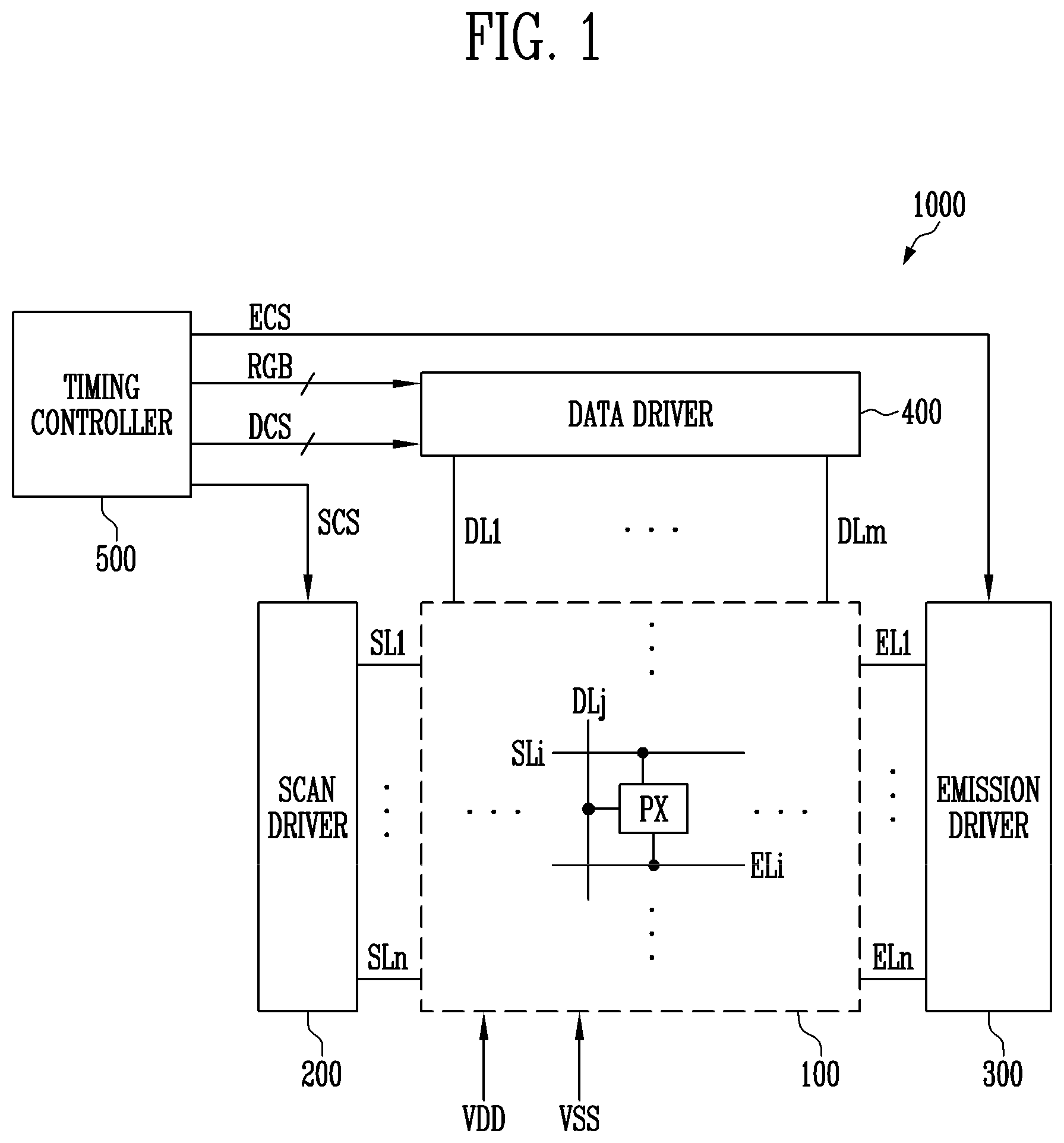
is a block diagram illustrating a display device 1000 according to embodiments of the disclosure.
Referring to , the display device 1000 may include a pixel unit 100 , a scan driver 200 (or a first gate driver), an emission driver 300 (or a second gate driver), a data driver 400 , and a timing controller 500 .
Hereinafter, the scan driver 200 and the emission driver 300 may be understood as one configuration of a gate driver.
The display device 1000 may display an image at various driving frequencies (image refresh rates, or screen refresh rates) according to a driving condition. The driving frequency is a frequency at which a data signal is substantially written to a driving transistor of a pixel PX. For example, the driving frequency may also be referred to as a screen scan rate or a screen refresh frequency, and may indicate a frequency at which a display screen is refreshed for one second. The display device 1000 may display an image in correspondence with various driving frequencies.
In an embodiment, an output frequency of the data driver 400 for one horizontal line (or pixel row) and/or an output frequency of the scan driver 200 outputting a scan signal may be determined in correspondence with the image refresh rate. For example, a refresh rate for driving a moving image may be a frequency of about 60 Hz or higher (for example, 80 Hz, 96 Hz, 120 Hz, 240 Hz, or the like).
In an embodiment, the display device 1000 may adjust the output frequency of the scan driver 200 for one horizontal line (or pixel row) and the output frequency of the data driver 400 corresponding thereto according to a driving condition. For example, the display device 1000 may display an image in correspondence with various image refresh rates of 1 Hz to 240 Hz. However, the display device 1000 may display an image at an image refresh rate of 240 Hz or higher (for example, 480 Hz) in an embodiment.
The pixel unit 100 may display an image. The pixel unit 100 may include pixels PX positioned to be connected to data lines DL 1 to DLm, scan lines SL 1 to SLn, and emission control lines EL 1 to ELn. The pixels PX may receive voltages of first driving power VDD, second driving power VSS, and initialization power from the outside. In an embodiment, a voltage level of the second driving power VSS may be lower than a voltage level of the first driving power VDD. For example, the voltage of the first driving power VDD may be a positive voltage, and the voltage of the second driving power VSS may be a negative voltage.
Additionally, the pixels PX may be connected to one or more scan lines SLi and emission control lines ELi in correspondence with a pixel circuit structure. The pixel PX may include a driving transistor, a plurality of switching transistors implemented as at least one of an n-type transistor and a p-type transistor, and a light emitting element.
The timing controller 500 may receive an input control signal and an input image signal from an image source such as an external graphic device. The timing controller 500 may generate image data RGB suitable for an operation condition of the pixel unit 100 based on the input image signal and provide the image data RGB to the data driver 400 . The timing controller 500 may generate a first control signal SCS for controlling a driving timing of the scan driver 200 , a second control signal ECS for controlling a driving timing of the emission driver 300 , and a third control signal DCS for controlling a driving timing of the data driver 400 , based on the input control signal. The timing controller 500 may provide the first control signal SCS, the second control signal ECS, and the third control signal DCS to the scan driver 200 , the emission driver 300 , and the data driver 400 , respectively.
The scan driver 200 may receive the first control signal SCS from the timing controller 500 . The scan driver 200 may supply a scan signal to the scan lines SL 1 to SLn in response to the first control signal SCS. The first control signal SCS may include a start pulse and a plurality of clock signals for the scan signal.
In an embodiment, the scan driver 200 may supply the scan signal to the scan lines SL 1 to SLn at the same frequency (for example, a second frequency) as the image refresh rate of the display device 1000 . Here, the scan signal may be a scan signal for writing a data signal to the driving transistor of the pixel PX. The second frequency may be set to a divisor of a first frequency for driving the emission driver 300 .
The scan driver 200 may supply a scan signal having a gate-on level of a pulse to the scan lines SL 1 to SLn in the display scan period of one frame. For example, the scan driver 200 may supply at least one scan signal to each of the scan lines SL 1 to SLn during the display scan period.
In addition, the scan driver 200 may supply a scan signal maintained as a gate-off level to the scan lines SL 1 to SLn during the self-scan period of one frame.
In an embodiment, the scan driver 200 may additionally supply a scan signal for initialization and/or compensation to the pixels PX.
The emission driver 300 may receive the second control signal ECS from the timing controller 500 . The emission driver 300 may supply an emission control signal to the emission control lines EL 1 to ELn in response to the second control signal ECS. The second control signal ECS may include a start pulse and a plurality of clock signals for the emission control signal.
In an embodiment, the emission driver 300 may supply the emission control signal to the emission control lines EL 1 to ELn at the first frequency. For example, the emission driver 300 may always supply the emission control signal to the emission control lines EL 1 to ELn at a constant frequency (for example, the first frequency) regardless of a frequency of the image refresh rate. Therefore, within one frame, the emission control signals supplied to the emission control lines EL 1 to ELn may be repeatedly supplied for each predetermined period.
In addition, the first frequency may be set higher than the second frequency. In an embodiment, the frequency (or the second frequency) of the image refresh rate may be set to a divisor of the first frequency.
For example, at all driving frequencies at which the display device 1000 may be driven, the emission driver 300 may perform scanning once during the display scan period, and perform scanning at least once during the self-scan period according to the image refresh rate.
That is, the emission control signal may be sequentially output to each of the emission control lines EL 1 to ELn once during the display scan period, and the emission control signal may be sequentially output to each of the emission control lines EL 1 to ELn once or more during the self-scan period.
Accordingly, when the image refresh rate is decreased, the number of repetitions of an operation of the emission driver 300 supplying the emission control signal to each of the emission control lines EL 1 to ELn within one frame may increase.
The data driver 400 may receive the third control signal DCS from the timing controller 500 . The data driver 400 may convert the image data RGB into an analog data signal (for example, a data voltage) in response to the third control signal DCS and supply the data signal to the data lines DL 1 to DLm.
Meanwhile, in , for convenience of description, each of the scan driver 200 and the emission driver 300 is shown as a single configuration. However, according to design, the scan driver 200 may include a plurality of scan drivers each supplying at least one of scan signals of different waveforms. In addition, at least a portion of the scan driver 200 and the emission driver 300 may be integrated into one driving circuit, module, or the like.
In an embodiment, the display device 1000 may further include a power supply. The power supply may supply the voltage of the first driving power VDD and the voltage of the second driving power VSS for driving the pixel PX to the pixel unit 100 .
is a block diagram illustrating a scan driver 200 (gate driver) according to embodiments of the disclosure.
Meanwhile, for convenience of description, in , four stage groups STG 1 to STG 4 among, i.e., of, stage groups included in the scan driver 200 and scan signals (or output signals OUT 1 to OUT 8 ) output from the stage groups are exemplarily shown.
Meanwhile, the scan driver 200 is an example of the gate driver.
Referring to , the scan driver 200 may include a plurality of stage groups STG 1 to STG 4 . The stage groups STG 1 to STG 4 may be respectively connected to corresponding scan lines SL 1 to SLB, and may output a scan signal (or an output) corresponding to clock signals CLK 1 to CLK 4 and carry clock signals RCLK 1 to RCLK 4 .
In an embodiment, each of the stage groups STG 1 to STG 4 may include two stages. For example, a first stage group STG 1 may include a first stage ST 1 and a second stage ST 2 , a second stage group STG 2 may include a third stage ST 3 and a fourth stage ST 4 , a third stage group STG 3 may include a fifth stage ST 5 and a sixth stage ST 6 , and a fourth stage group STG 4 may include a seventh stage ST 7 and an eighth stage ST 8 . The first stage ST 1 and the second stage ST 2 included in the first stage group STG 1 may output a first scan signal (or a first output signal OUT 1 ) and a second scan signal (or a second output signal OUT 2 ) through a first scan line SL 1 and a second scan line SL 2 , respectively. The third stage ST 3 and the fourth stage ST 4 included in the second stage group STG 2 may output a third scan signal (or a third output signal OUT 3 ) and a fourth scan signal (or a fourth output signal OUT 4 ) through a third scan line SL 3 and a fourth scan line SL 4 , respectively. The fifth stage ST 5 and the sixth stage ST 6 included in the third stage group STG 3 may output a fifth scan signal (or a fifth output signal OUT 5 ) and a sixth scan signal (or a sixth output signal OUT 6 ) through a fifth scan line SL 5 and a sixth scan line SL 6 , respectively. The seventh stage ST 7 and the eighth stage ST 8 included in the fourth stage group STG 4 may output a seventh scan signal (or a seventh output signal OUT 7 ) and an eighth scan signal (or an eighth output signal OUT 8 ) through a seventh scan line SL 7 and an eighth scan line SLB, respectively.
In an embodiment, each of the stage groups STG 1 to STG 4 may include an output control circuit (or an output control unit). For example, the first stage group STG 1 may include a first output control circuit OCC 1 , the second stage group STG 2 may include a second output control circuit OCC 2 , the third stage group STG 3 may include a third output control circuit OCC 3 , and the fourth stage group STG 4 may include a fourth output control circuit OCC 4 . Each of the output control circuits OCC 1 to OCC 4 may control a voltage level of an output control node (for example, a first node QB_A or a second node QB_B of ) included in each of the stages included in a corresponding stage group.
According to an embodiment, the two stages included in each of the stage groups STG 1 to STG 4 may share one output control circuit.
For example, the first stage ST 1 and the second stage ST 2 included in the first stage group STG 1 may share the first output control circuit OCC 1 . The third stage ST 3 and the fourth stage ST 4 included in the second stage group STG 2 may share the second output control circuit OCC 2 . The fifth stage ST 5 and the sixth stage ST 6 included in the third stage group STG 3 may share the third output control circuit OCC 3 . The seventh stage ST 7 and the eighth stage ST 8 included in the fourth stage group STG 4 may share the fourth output control circuit OCC 4 .
As described above, since the two stages included in each of the stage groups STG 1 to STG 4 share one output control circuit, the voltage level of the output control node (for example, the first node QB_A or the second node QB_B of ) included in each of the two stages included in one stage group may be controlled by one output control circuit. Accordingly, a dead space of the scan driver 200 (or the stage groups STG 1 to STG 4 ) may be reduced (or minimized).
A configuration in which the voltage level of the output control node included in each of the stages is controlled according to an operation of the output control circuit is specifically described with reference to , 6 A , and 6 B.
The second stage group STG 2 may be connected in dependence on the first stage group STG 1 , the third stage group STG 3 may be connected in dependence on the second stage group STG 2 , and the fourth stage group STG 4 may be connected in dependence on the third stage group STG 3 . The first to fourth stage groups STG 1 to STG 4 may have substantially the same configuration. For example, the stages ST 1 to ST 8 included in each of the stage groups STG 1 to STG 4 may have substantially the same configuration.
Each of the stage groups STG 1 to STG 4 may include a first input terminal 201 , a second input terminal 202 , a third input terminal 203 , a fourth input terminal 204 , a first power input terminal 205 , a second power input terminal 206 , a third power input terminal 207 , a first output terminal 208 , and a second output terminal 209 .
In an embodiment, each of the stage groups STG 1 to STG 4 may further include a fifth input terminal 210 , a sixth input terminal 211 , and a seventh input terminal 212 .
According to an embodiment, the two stages included in each of the stage groups STG 1 to ST 4 may be commonly connected to the fourth input terminal 204 , the seventh input terminal 212 , the first power input terminal 205 , the second power input terminal 206 , and the third power input terminal 207 . In addition, the output control circuit included in each of the stage groups STG 1 to ST 4 may be connected to the fifth input terminal 210 and the sixth input terminal 211 .
In an embodiment, the first input terminal 201 included in each of the stage groups STG 1 to STG 4 may include a first sub-input terminal 201 a and a second sub-input terminal 201 b , the second input terminal 202 may include a third sub-input terminal 202 a and a fourth sub-input terminal 202 b , and the third input terminal 203 may include a fifth sub-input terminal 203 a and a sixth sub-input terminal 203 b . Each the sub-input terminal may be connected to a corresponding stage among the stages included in each of the stage groups STG 1 to STG 4 .
For example, the first stage ST 1 of the stages ST 1 and ST 2 included in the first stage group STG 1 may be connected to the first sub-input terminal 201 a , the third sub-input terminal 202 a , and the fifth sub-input terminal 203 a . In addition, the second stage ST 2 of the stages ST 1 and ST 2 included in the first stage group STG 1 may be connected to the second sub-input terminal 201 b , the fourth sub-input terminal 202 b , and the sixth sub-input terminal 203 b . Each of the stages included in the second to fourth stage groups STG 2 , STG 3 , and STG 4 may also be connected to sub-input terminals in substantially the same form.
In addition, the first output terminal 208 included in each of the stage groups STG 1 to STG 4 may include a first sub-output terminal 208 a and a second sub-output terminal 208 b , and the second output terminal 209 may include a third sub-output terminal 209 a and a fourth sub-output terminal 209 b . Each the sub-output terminals may be connected to a corresponding stage among the stages included in each of the stage groups STG 1 to STG 4 .
For example, the first stage ST 1 of the stages ST 1 and ST 2 included in the first stage group STG 1 may be connected to the first sub-output terminal 208 a to output the first scan signal (or the first output signal OUT 1 ) to the first sub-output terminal 208 a , and may be connected to the third sub-output terminal 209 a to output a first carry signal CR 1 to the third sub-output terminal 209 a . In addition, the second stage ST 2 of the stages ST 1 and ST 2 included in the first stage group STG 1 may be connected to the second sub-output terminal 208 b to output the second scan signal (or the second output signal OUT 2 ) to the second sub-output terminal 208 b , and may be connected to the fourth sub-output terminal 209 b to output the second carry signal CR 2 to the fourth sub-output terminal 209 b . The stages included in the second to fourth stage groups STG 2 , STG 3 , and STG 4 may also be connected to the sub-output terminals in substantially the same form.
The first input terminal 201 of the first stage group STG 1 may receive a start pulse SP. For example, each of the first sub-input terminal 201 a and the second sub-input terminal 201 b of the first stage group STG 1 may receive the start pulse SP. Accordingly, the first stage ST 1 included in the first stage group STG 1 may receive the start pulse SP through the first sub-input terminal 201 a , and the second stage ST 2 included in the first stage group STG 1 may receive the start pulse SP through the second sub-input terminal 201 b.
In addition, each of the first input terminals 201 of the second to fourth stage groups STG 2 to STG 4 may receive carry signals output from the second output terminal 209 of a previous stage group.
For example, the first input terminal 201 of the second stage group STG 2 may receive the first carry signal CR 1 and a second carry signal CR 2 output from the second output terminal 209 of the first stage group STG 1 . For example, the first sub-input terminal 201 a of the second stage group STG 2 may receive the first carry signal CR 1 output from the third sub-output terminal 209 a of the first stage group STG 1 , and the second sub-input terminal 201 b of the second stage group STG 2 may receive the second carry signal CR 2 output from the fourth sub-output terminal 209 b of the first stage group STG 1 . Accordingly, the third stage ST 3 included in the second stage group STG 2 may receive the first carry signal CR 1 through the first sub-input terminal 201 a , and the fourth stage ST 4 included in the second stage group STG 2 may receive the second carry signal CR 2 through the second sub-input terminal 201 b.
As another example, the first input terminal 201 of the third stage group STG 3 may receive a third carry signal CR 3 and a fourth carry signal CR 4 output from the second output terminal 209 of the second stage group STG 2 . For example, the first sub-input terminal 201 a of the third stage group STG 3 may receive the third carry signal CR 3 output from the third sub-output terminal 209 a of the second stage group STG 2 , and the second sub-input terminal 201 b of the third stage group STG 3 may receive the fourth carry signal CR 4 output from the fourth sub-output terminal 209 b of the second stage group STG 2 . Accordingly, the fifth stage ST 5 included in the third stage group STG 3 may receive the third carry signal CR 3 through the first sub-input terminal 201 a , and the sixth stage ST 6 included in the third stage group STG 3 may receive the fourth carry signal CR 4 through the second sub-input terminal 201 b.
As still another example, the first input terminal 201 of the fourth stage group STG 4 may receive a fifth carry signal CR 5 and a sixth carry signal CR 6 output from the second output terminal 209 of the third stage group STG 3 . For example, the first sub-input terminal 201 a of the fourth stage group STG 4 may receive the fifth carry signal CR 5 output from the third sub-output terminal 209 a of the third stage group STG 3 , and the second sub-input terminal 201 b of the fourth stage group STG 4 may receive the sixth carry signal CR 6 output from the fourth sub-output terminal 209 b of the third stage group STG 3 . Accordingly, the seventh stage ST 7 included in the fourth stage group STG 4 may receive the fifth carry signal CR 5 through the first sub-input terminal 201 a , and the eighth stage ST 8 included in the fourth stage group STG 4 may receive the sixth carry signal CR 6 through the second sub-input terminal 201 b.
First and second clock signals CLK 1 and CLK 2 or third and fourth clock signals CLK 3 and CLK 4 among clock signals CLK 1 to CLK 4 may be provided to the second input terminal 202 of the stage groups STG 1 to STG 4 .
In an embodiment, the second input terminal 202 of a k-th stage group, where k is an integer greater than 0, may receive the first clock signal CLK 1 and the second clock signal CLK 2 . For example, the third sub-input terminal 202 a of the k-th stage group may receive the first clock signal CLK 1 , and the fourth sub-input terminal 202 b of the k-th stage group may receive the second clock signal CLK 2 . On the other hand, the second input terminal 202 of a (k+1)-th stage group may receive the third clock signal CLK 3 and the fourth clock signal CLK 4 . For example, the third sub-input terminal 202 a of the (k+1)-th stage group may receive the third clock signal CLK 3 , and the fourth sub-input terminal 202 b of the (k+1)-th stage group may receive the fourth clock signal CLK 4 .
For example, each of the second input terminals 202 of the first stage group STG 1 and the third stage group STG 3 may receive the first and second clock signals CLK 1 and CLK 2 . For example, the third sub-input terminals 202 a of the first stage group STG 1 and the third stage group STG 3 may receive the first clock signal CLK 1 , and the fourth sub-input terminals 202 b of the first stage group STG 1 and the third stage group STG 3 may receive the second clock signal CLK 2 . On the other hand, each of the second input terminals 202 of the fourth stage group STG 4 may receive the third and fourth clock signals CLK 3 and CLK 4 . For example, the third sub-input terminals 202 a of the second stage group STG 2 and the fourth stage group STG 4 may receive the third clock signal CLK 3 , and the fourth sub-input terminals 202 b of the second stage group STG 2 and the fourth stage group STG 4 may receive the fourth clock signal CLK 4 .
Accordingly, an s-th stage, where s is an integer greater than 0, included in the k-th stage group may receive the first clock signal CLK 1 through the third sub-input terminal 202 a of the second input terminal 202 , and an (s+1)-th stage included in the k-th stage group may receive the second clock signal CLK 2 through the fourth sub-input terminal 202 b of the second input terminal 202 .
In addition, an (s+2)-th stage included in the (k+1)-th stage group may receive the third clock signal CLK 3 through the third sub-input terminal 202 a of the second input terminal 202 , and an (s+3)-th stage included in the (k+1)-th stage group may receive the fourth clock signal CLK 4 through the fourth sub-input terminal 202 b of the second input terminal 202 .
That is, the first to fourth clock signals CLK 1 to CLK 4 may be sequentially provided to the s-th stage, the (s+1)-th stage, the (s+2)-th stage, and the (s+3)-th stage included in two adjacent stage groups, for example, the k-th stage group and the (k+1)-th stage group.
For example, each of the first stage ST 1 included in the first stage group STG 1 and the fifth stage ST 5 included in the third stage group STG 3 may receive the first clock signal CLK 1 through the third sub-input terminal 202 a , and each of the second stage ST 2 included in the first stage group STG 1 and the sixth stage ST 6 included in the third stage group STG 3 may receive the second clock signal CLK 2 through the fourth sub-input terminal 202 b.
In addition, each of the third stage ST 3 included in the second stage group STG 2 and the seventh stage ST 7 included in the fourth stage group STG 4 may receive the third clock signal CLK 3 through the third sub-input terminal 202 a , and each of the fourth stage ST 4 included in the second stage group STG 2 and the eighth stage ST 8 included in the fourth stage group STG 4 may receive the fourth clock signal CLK 4 through the fourth sub-input terminal 202 b.
That is, the first to fourth clock signals CLK 1 to CLK 4 may be sequentially provided to the first to fourth stages ST 1 to ST 4 , and the first to fourth clock signals CLK 1 to CLK 4 may be sequentially provided to the fifth to eighth stages ST 5 to ST 8 .
In an embodiment, the clock signals CLK 1 to CLK 4 may have the same period in a display scan period DSP (refer to A ) and have a waveform in which a phase partially overlaps. For example, in the display scan period DSP (refer to A ), the second clock signal CLK 2 may be set to a signal shifted by about 1/4 period from the first clock signal CLK 1 , the third clock signal CLK 3 may be set to a signal shifted by about 1/4 period from the second clock signal CLK 2 , and the fourth clock signal CLK 4 may be set to a signal shifted by about 1/4 period from the third clock signal CLK 3 .
In an embodiment, the clock signals CLK 1 to CLK 4 may have a waveform maintained as a constant level during a self-scan period SSP (refer to B ). For example, in the self-scan period SSP (refer to B ), the clock signals CLK 1 to CLK 4 may be set to a signal maintained as a low level (or a low voltage).
First and second carry clock signals RCLK 1 and RCLK 2 or third and fourth carry clock signals RCLK 3 and RCLK 4 among carry clock signals RCLK 1 to RCLK 4 may be provided to the third input terminal 203 of the stage groups STG 1 to STG 4 .
In an embodiment, the third input terminal 203 of the k-th stage group may receive the first carry clock signal RCLK 1 and the second carry clock signal RCLK 2 . For example, the fifth sub-input terminal 203 a of the k-th stage group may receive the first carry clock signal RCLK 1 , and the sixth sub-input terminal 203 b of the k-th stage group may receive the second carry clock signal RCLK 2 . On the other hand, the third input terminal 203 of the (k+1)-th stage group may receive the third carry clock signal RCLK 3 and the fourth carry clock signal RCLK 4 . For example, the fifth sub-input terminal 203 a of the (k+1)-th stage group may receive the third carry clock signal RCLK 3 , and the sixth sub-input terminal 203 b of the (k+1)-th stage group may receive the fourth carry clock signal RCLK 4 .
For example, each of the third input terminals 203 of the first stage group STG 1 and the third stage group STG 3 may receive the first and second carry clock signals RCLK 1 and RCLK 2 . For example, the fifth sub-input terminals 203 a of the first stage group STG 1 and the third stage group STG 3 may receive the first carry clock signal RCLK 1 , and the sixth sub-input terminals 203 b of the first stage group STG 1 and the third stage group STG 3 may receive the second carry clock signal RCLK 2 . On the other hand, each of the third input terminals 203 of the second stage group STG 2 and the fourth stage group STG 4 may receive the third and fourth carry clock signals RCLK 3 and RCLK 4 . For example, the fifth sub-input terminals 203 a of the second stage group STG 2 and the fourth stage group STG 4 may receive the third carry clock signal RCLK 3 , and the sixth sub-input terminals 203 b of the second stage group STG 2 and the fourth stage group STG 4 may receive the fourth carry clock signal RCLK 4 .
Accordingly, the s-th stage included in the k-th stage group may receive the first carry clock signal RCLK 1 through the fifth sub-input terminal 203 a of the third input terminal 203 , and the (s+1)-th stage included in the k-th stage group may receive the second carry clock signal RCLK 2 through the sixth sub-input terminal 203 b of the third input terminal 203 .
In addition, the (s+2)-th stage included in the (k+1)-th stage group may receive the third carry clock signal RCLK 3 through the fifth sub-input terminal 203 a of the third input terminal 203 , and the (s+3)-th stage included in the (k+1)-th stage group may receive the fourth carry clock signal RCLK 4 through the sixth sub-input terminal 203 b of the third input terminal 203 .
That is, the first to fourth carry clock signals RCLK 1 to RCLK 4 may be sequentially provided to the s-th stage, the (s+1)-th stage, the (s+2)-th stage, and the (s+3)-th stage included in two adjacent stage groups, for example, the k-th stage group and the (k+1)-th stage group.
For example, each of the first stage ST 1 included in the first stage group STG 1 and the fifth stage ST 5 included in the third stage group STG 3 may receive the first carry clock signal RCLK 1 through the fifth sub-input terminal 203 a , and each of the second stage ST 2 included in the first stage group STG 1 and the sixth stage ST 6 included in the third stage group STG 3 may receive the second carry clock signal RCLK 2 through the sixth sub-input terminal 203 b.
In addition, each of the third stage ST 3 included in the second stage group STG 2 and the seventh stage ST 7 included in the fourth stage group STG 4 may receive the third carry clock signal RCLK 3 through the fifth sub-input terminal 203 a , and each of the fourth stage ST 4 included in the second stage group STG 2 and the eighth stage ST 8 included in the fourth stage group STG 4 may receive the fourth carry clock signal RCLK 4 through the sixth sub-input terminal 203 b.
That is, the first to fourth carry clock signals RCLK 1 to RCLK 4 may be sequentially provided to the first to fourth stages ST 1 to ST 4 , and the first to fourth carry clock signals RCLK 1 to RCLK 4 may be sequentially provided to the fifth to eighth stages ST 5 to ST 8 .
In an embodiment, the carry clock signals RCLK 1 to RCLK 4 may have the same period in the display scan period DSP (refer to A ), and may have a waveform in which a phase partially overlaps. For example, in the display scan period DSP (refer to A ), the second carry clock signal RCLK 2 may be set to a signal shifted by about 1/4 period from the first carry clock signal RCLK 1 , the third carry clock signal RCLK 3 may be set to a signal shifted by about 1/4 period from the second carry clock signal RCLK 2 , and the fourth carry clock signal RCLK 4 may be set to a signal shifted by about 1/4 period from the third carry clock signal RCLK 3 .
In an embodiment, the carry clock signals RCLK 1 to RCLK 4 may have a waveform maintained as a constant level during the self-scan period SSP (refer to B ). For example, in the self-scan period SSP (refer to B ), the carry clock signals RCLK 1 to RCLK 4 may be set to a signal maintained as a high level (or a high voltage).
As described with reference to , according to the image refresh rate of the display device 1000 (refer to ), the scan driver 200 may supply the scan signal having the pulse of the gate-on level (for example, the high level) to the scan lines SL 1 to SL 8 in the display scan period DSP (refer to A ) of one frame, and supply the scan signal maintained as the gate-off level (for example, the low level) to the scan lines SL 1 to SL 8 in the self-scan period SSP (refer to B ) of one frame. Here, the display device 1000 (refer to ) (or the scan driver 200 ) according to embodiments of the disclosure may maintain the clock signals CLK 1 to CLK 4 and the carry clock signals RCLK 1 to RCLK 4 used to generate the scan signal as a constant level during the self-scan period in which the scan signals (or the output signals OUT 1 to OUT 8 ) are maintained as the gate-off level (or the low level). Therefore, power consumption for transiting (or clocking) a signal level of the clock signals CLK 1 to CLK 4 and a signal level of the carry clock signals RCLK 1 to RCLK 4 to a constant period may be reduced. This is specifically described with reference to A to 7 B .
Each of the fourth input terminals 204 of the stage groups STG 1 to STG 4 may receive a carry signal output from the second output terminal 209 (for example, the fourth sub-output terminal 209 b ) of a next stage group.
In an embodiment, the fourth input terminal 204 of the k-th stage group may receive the carry signal output from the fourth sub-output terminal 209 b of the (k+1)-th stage group. Accordingly, the s-th stage and the (s+1)-th stage included in the k-th stage group may receive an (s+3)-th carry signal output from the (s+3)-th stage through the fourth sub-output terminal 209 b of the (k+1)-th stage group.
For example, the fourth input terminal 204 of the first stage group STG 1 may receive the fourth carry signal CR 4 output from the fourth sub-output terminal 209 b of the second stage group STG 2 . That is, the fourth input terminal 204 of the first stage group STG 1 may receive the fourth carry signal CR 4 output from the fourth stage ST 4 included in the second stage group STG 2 . Accordingly, each of the first stage ST 1 and the second stage ST 2 included in the first stage group STG 1 may receive the fourth carry signal CR 4 through the fourth input terminal 204 .
As another example, the fourth input terminal 204 of the second stage group STG 2 may receive the sixth carry signal CR 6 output from the fourth sub-output terminal 209 b of the third stage group STG 3 . That is, the fourth input terminal 204 of the second stage group STG 2 may receive the sixth carry signal CR 6 output from the sixth stage ST 6 included in the third stage group STG 3 . Accordingly, each of the third stage ST 3 and the fourth stage ST 4 included in the second stage group STG 2 may receive the sixth carry signal CR 6 through the fourth input terminal 204 .
As still another example, the fourth input terminal 204 of the third stage group STG 3 may receive an eighth carry signal CR 8 output from the fourth sub-output terminal 209 b of the fourth stage group STG 4 . That is, the fourth input terminal 204 of the third stage group STG 3 may receive the eighth carry signal CR 8 output from the eighth stage ST 8 included in the fourth stage group STG 4 . Accordingly, each of the fifth stage ST 5 and the sixth stage ST 6 included in the third stage group STG 3 may receive the eighth carry signal CR 8 through the fourth input terminal 204 .
As still another example, the fourth input terminal 204 of the fourth stage group STG 4 may receive a tenth carry signal CR 10 output from the fourth sub-output terminal of a next stage group, for example, a fifth stage group. That is, the fourth input terminal 204 of the fourth stage group STG 4 may receive the tenth carry signal CR 10 output from a tenth stage included in the fifth stage group. Accordingly, each of the seventh stage ST 7 and the eighth stage ST 8 included in the fourth stage group STG 4 may receive the tenth carry signal CR 10 through the fourth input terminal 204 .
However, in an embodiment, the s-th stage and the (s+1)-th stage included in the k-th stage group may receive a q-th carry signal output from a q-th stage, where q is an integer greater than p+3, through the fourth input terminal 204 .
Voltages of power required for driving the stage groups STG 1 to STG 4 (or the stages ST 1 to ST 8 ) may be applied to the first to third power input terminals 205 , 206 , and 207 of the stage groups STG 1 to STG 4 .
For example, a voltage of first power VGL 1 may be applied to the first power input terminal 205 of each of the stage groups STG 1 to STG 4 , a voltage of second power VGL 2 may be applied to the second power input terminal 206 of each of the stage groups STG 1 to STG 4 , and a voltage of third power VGH may be applied to the third power input terminal 207 of each of the stage groups STG 1 to STG 4 . Accordingly, the voltage of the first power VGL 1 , the voltage of the second power VGL 2 , and the voltage of the third power VGH may be applied to the stages ST 1 to ST 8 included in the stage groups STG 1 to STG 4 .
The voltage of the first power VGL 1 , the voltage of the second power VGL 2 , and the voltage of the third power VGH may have a DC voltage level. Here, a voltage level of the third power VGH may be set higher than a voltage level of the first power VGL 1 and the second power VGL 2 . In an embodiment, the voltage level of the second power VGL 2 may be set equal to the voltage level of the first power VGL 1 or lower than the voltage level of the first power VGL 1 .
The output signals OUT 1 to OUT 8 may be output to the first output terminals 208 , for example, the first and second sub-output terminals 208 a and 208 b , of each of the stage groups STG 1 to STG 4 . In an embodiment, the output signals OUT 1 to OUT 8 output to the first output terminals 208 may be provided to the corresponding scan lines SL 1 to SL 8 as the scan signals.
The carry signals CR 1 to CR 8 may be output to the second output terminals 209 of each of the stage groups STG 1 to STG 4 . As described above, each of the carry signals CR 1 to CR 8 output to the second output terminals 209 may be provided to the first input terminals 201 of a next stage group. For example, the first carry signal CR 1 and the second carry signal CR 2 output from the second output terminal 209 of the first stage group STG 1 may be provided to the first input terminal 201 of the second stage group STG 2 . For example, the first carry signal CR 1 output from the third sub-output terminal 209 a of the first stage group STG 1 may be provided to the first sub-input terminal 201 a of the second stage group STG 2 , and the second carry signal CR 2 output from the fourth sub-output terminal 209 b of the first stage group STG 1 may be provided to the second sub-input terminal 201 b of the second stage group STG 2 . In addition, the third carry signal CR 3 and the fourth carry signal CR 4 output from the second output terminal 209 of the second stage group STG 2 may be provided to the first input terminal 201 of the third stage group STG 3 . For example, the third carry signal CR 3 output from the third sub-output terminal 209 a of the second stage group STG 2 may be provided to the first sub-input terminal 201 a of the third stage group STG 3 , and the fourth carry signal CR 4 output from the fourth sub-output terminal 209 b of the second stage group STG 2 may be provided to the second sub-input terminal 201 b of the third stage group STG 3 . In addition, the fifth carry signal CR 5 and the sixth carry signal CR 6 output from the second output terminal 209 of the third stage group STG 3 may be provided to the first input terminal 201 of the fourth stage group STG 4 . For example, the fifth carry signal CR 5 output from the third sub-output terminal 209 a of the third stage group STG 3 may be provided to the first sub-input terminal 201 a of the fourth stage group STG 4 , and the sixth carry signal CR 6 output from the fourth sub-output terminal 209 b of the third stage group STG 3 may be provided to the second sub-input terminal 201 b of the fourth stage group STG 4 . Similarly to this, the seventh carry signal CR 7 and the eighth carry signal CR 8 output from the second output terminal 209 of the fourth stage group STG 4 may be provided to the first input terminal of the fifth stage group.
A first node control signal GBI 1 and a second node control signal GBI 2 may be provided to the fifth input terminal 210 and the sixth input terminal 211 of the stage groups STG 1 to STG 4 , respectively.
In an embodiment, the first node control signal GBI 1 and the second node control signal GBI 2 may have opposite signal levels. For example, when the first node control signal GBI 1 has a high level, the second node control signal GBI 2 may have a low level. As another example, when the first node control signal GBI 1 has a low level, the second node control signal GBI 2 may have a high level. However, in an example, the first node control signal GBI 1 and the second node control signal GBI 2 may have the same signal level, for example, a high level. As another example, the first node control signal GBI 1 and the second node control signal GBI 2 may have opposite signal levels in a partial section, and may have the same signal level in another partial section.
In an embodiment, each of the signal level of the first node control signal GBI 1 and the signal level of the second node control signal GBI 2 may vary in a frame unit. For example, the first node control signal GBI 1 may be maintained as a high level during one frame, and may transit to a low level by varying the signal level of the first node control signal GBI 1 in a next frame of the corresponding frame. Similarly, the second node control signal GBI 2 may be maintained as a low level during one frame, and may transit to a high level by varying the signal level of the second node control signal GBI 2 in a next frame of the corresponding frame. However, an embodiment of the disclosure is not limited thereto, and the signal level of the first node control signal GBI 1 and the second node control signal GBI 2 may vary in two or more frame units. The first node control signal GBI 1 and the second node control signal GBI 2 are specifically described with reference to A to 8 B .
An initialization control signal SESR may be provided to the seventh input terminal 212 of the stage groups STG 1 to STG 4 . The initialization control signal SESR may be provided to the stage groups STG 1 to STG 4 through the seventh input terminal 212 at least once when the display device 1000 (refer to ) (or the scan driver 200 ) is powered on, and may not be provided thereafter.
In an embodiment, the stage groups STG 1 to STG 4 , for example, stages ST 1 to ST 8 , included in the scan driver 200 may have substantially the same configuration except for a type of a signal received through the first input terminal 201 , for example, the first and second sub-input terminals 201 a and 201 b . For example, the first stage group STG 1 that is an initial stage that receives the start pulse SP through the first input terminal 201 and the remaining stages, for example, second to fourth stage groups STG 2 to STG 4 , that receive the carry signals of a previous stage through the first input terminal 201 may have substantially the same circuit configuration and may operate substantially identically except for the input signal (that is, the start pulse SP or the carry signals of the previous stage group) through the first input terminal 201 .
Accordingly, hereinafter, for convenience of description, in describing the stage groups (or stages) included in the scan driver 200 , the first stage group STG 1 is described as a reference.
is a circuit diagram illustrating an example of the first stage group included in the scan driver of . A and 4 B are diagrams illustrating an example of a transistor included in the first stage group of .
Referring to , the first stage group STG 1 may include the first stage ST 1 and the second stage ST 2 . In an embodiment, the first stage group STG 1 may further include the first output control circuit OCC 1 .
The first stage ST 1 may include a first input unit 11 , a first output unit 12 (or a first scan signal output unit), a second output unit 13 (or a first carry signal output unit), and a first capacitor C 1 (or a first boosting capacitor). According to embodiments, the first stage ST 1 may further include a first initialization unit 14 and a first stabilization unit 15 .
The second stage ST 2 may include a second input unit 21 , a third output unit 22 (or a second scan signal output unit), a fourth output unit 23 (or a second carry signal output unit), and a fourth capacitor C 4 (or a second boosting capacitor). According to embodiments, the second stage ST 2 may further include a second initialization unit 24 and a second stabilization unit 25 .
The first stage ST 1 may generate and output the first carry signal CR 1 and the first output signal OUT 1 (or the first scan signal), based on an input signal IN, a first carry clock signal RCLK 1 , a first clock signal CLK 1 , the voltage of the first power VGL 1 , the voltage of the second power VGL 2 , and the voltage of the third power VGH.
The second stage ST 2 may generate and output the second carry signal CR 2 and the second output signal OUT 2 (or the second scan signal), based on the input signal IN, a second carry clock signal RCLK 2 , a second clock signal CLK 2 , the voltage of the first power VGL 1 , the voltage of the second power VGL 2 , and the voltage of the third power VGH.
Meanwhile, as described with reference to , the voltage level of the third power VGH may be set higher than the voltage level of the first power VGL 1 and the second power VGL 2 , for example, set to a high voltage. In addition, the voltage level of the second power VGL 2 may be set equal to the voltage level of the first power VGL 1 or lower than the voltage level of the first power VGL 1 . Hereinafter, for convenience of description, the description is given based on a case in which the voltage level of the first power VGL 1 and the voltage level of the second power VGL 2 are the same, for example, the same low voltage.
In an embodiment, the first stage ST 1 and the second stage ST 2 included in the first stage group STG 1 may be commonly connected to the same node. For example, the first stage ST 1 and the second stage ST 2 may be commonly connected to the first node QB_A and the second node QB_B.
According to an embodiment, a signal level of the first output signal OUT 1 and the first carry signal CR 1 output by the first stage ST 1 may be controlled based on a voltage of the first node QB_A, a voltage of the second node QB_B, and a voltage of a third node QA 1 , and a signal level of the second output signal OUT 2 and the second carry signal CR 2 output by the stage ST 2 may be controlled based on the voltage of the first node QB_A, the voltage of the second node QB_B, and a voltage of a fourth node QA 2 . That is, an operation of the first output unit 12 and the second output unit 13 of the first stage ST 1 may be controlled based on the voltage of the first node QB_A, the voltage of the second node QB_B, and a voltage of the third node QA 1 . In addition, an operation of the third output unit 22 and the fourth output unit 23 of the second stage ST 2 may be controlled based on the voltage of the first node QB_A, the voltage of the second node QB_B, and a voltage of the fourth node QA 2 .
In an embodiment, the first output control circuit OCC 1 may control the voltage of the first node QB_A and the voltage of the second node QB_B based on the first node control signal GBI 1 , the second node control signal GBI 2 , the first power VGL 1 , and the second power VGL 2 . For example, the first output control circuit OCC 1 may control the operation of the first output unit 12 and the second output unit 13 of the first stage ST 1 by controlling the voltage of the first node QB_A and the voltage of the second node QB_B. In addition, the first output control circuit OCC 1 may control the operation of the third output unit 22 and the fourth output unit 23 of the second stage ST 2 by controlling the voltage of the first node QB_A and the voltage of the second node QB_B.
As described above, according to embodiments of the disclosure, an operation of two adjacent stages, for example, the first stage ST 1 and the second stage ST 2 , may be controlled by one output control circuit, for example, the first output control circuit OCC 1 . For example, an operation in which the two adjacent stages, for example, the first stage ST 1 and the second stage ST 2 , output the scan signal and the carry signal may be controlled by one output control circuit, for example, the first output control circuit OCC 1 . Accordingly, a dead space of the scan driver 200 may be minimized.
Hereinafter, with reference to , the first stage ST 1 , the second stage ST 2 , and the first output control circuit OCC 1 included in the first stage group STG 1 are more specifically described. In addition, an operation of the first stage ST 1 , the second stage ST 2 , and the first output control circuit OCC 1 is specifically described with reference to to 7 B .
In an embodiment, the first stage ST 1 may include the first input unit 11 , the first output unit 12 , the second output unit 13 , and the first capacitor C 1 .
The first input unit 11 may receive a first input signal IN 1 , for example, the start pulse SP, through the first input terminal 201 , for example, the first sub-input terminal 201 a , receive a second input signal IN 2 , for example, the fourth carry signal CR 4 , through the fourth input terminal 204 , and receive the voltage of the second power VGL 2 through the second power input terminal 206 .
In an embodiment, the first input unit 11 may control the voltage of the third node QA 1 , based on the start pulse SP, the fourth carry signal CR 4 , and the voltage of the second power VGL 2 .
For example, the first input unit 11 may include a first sub-input unit 11 a and a second sub-input unit 11 b.
The first sub-input unit 11 a may include a first transistor T 1 .
The first transistor T 1 may be connected between the first sub-input terminal 201 a and the third node QA 1 and may include a gate electrode connected to the first sub-input terminal 201 a . The first transistor T 1 may be turned on when the first input signal IN 1 (or the start pulse SP) supplied through the first sub-input terminal 201 a has a gate-on level, for example, a high level, to electrically connect the first sub-input terminal 201 a and the third node QA 1 .
In an embodiment, the first transistor T 1 may include a plurality of sub-transistors connected to each other in series. For example, the first transistor T 1 may include first and second sub-transistors T 1 _ 1 and T 1 _ 2 connected to each other in series. Each of the first and second sub-transistors T 1 _ 1 and T 1 _ 2 may include a gate electrode commonly connected to the first sub-input terminal 201 a , for example, referred to as a dual gate structure. Accordingly, a current leakage by the first transistor T 1 may be minimized.
The second sub-input unit 11 b may include a second transistor T 2 .
The second transistor T 2 may be connected between the second power input terminal 206 and the third node QA 1 , and may include a gate electrode connected to the fourth input terminal 204 . The second transistor T 2 may be turned on when the second input signal IN 2 (or the fourth carry signal CR 4 ) supplied through the fourth input terminal 204 has a gate-on level, for example, a high level, to electrically connect the second power input terminal 206 and the third node QA 1 .
In an embodiment, the second transistor T 2 may include a plurality of sub-transistors connected to each other in series. For example, the second transistor T 2 may include third and fourth sub-transistors T 2 _ 1 and T 2 _ 2 connected to each other in series. Each of the third and fourth sub-transistors T 2 _ 1 and T 2 _ 2 may include a gate electrode commonly connected to the fourth input terminal 204 , for example, referred to as a dual gate structure. Accordingly, a current leakage by the second transistor T 2 may be minimized.
The first output unit 12 may be connected to the first node QB_A, the second node QB_B, and the third node QA 1 , may receive the first clock signal SLK 1 through the second input terminal 202 , for example, the third sub-input terminal 202 a , and may receive the voltage of the first power VGL 1 through the first power input terminal 205 .
The first output unit 12 may output the first output signal OUT 1 (or the first scan signal), based on the voltage of the first node QB_A, the voltage of the second node QB_B, the voltage of the third node QA 1 , the first clock signal CLK 1 , and the first power VGL 1 . For example, a high level of the first clock signal CLK 1 may correspond to a high level of the first output signal OUT 1 , and the voltage of the first power VGL 1 may correspond to a low level of the first output signal OUT 1 . The first output signal OUT 1 may be provided to the first scan line SL 1 through the first output terminal 208 , for example, the first sub-output terminal 208 a , as the scan signal.
To this end, the first output unit 12 may include third to fifth transistors T 3 to T 5 .
The third transistor T 3 may be connected between the third sub-input terminal 202 a and the first sub-output terminal 208 a , and may include a gate electrode connected to the third node QA 1 . The third transistor T 3 may be turned on or off based on the voltage of the third node QA 1 . When the third transistor T 3 is turned on, the third sub-input terminal 202 a and the first sub-output terminal 208 a may be electrically connected. When the first clock signal CLK 1 supplied through the third sub-input terminal 202 a has a high level when the third transistor T 3 is turned on, the high level of the first clock signal CLK 1 may correspond to the high level of the first output signal OUT 1 .
The fourth transistor T 4 may be connected between the first power input terminal 205 and the first sub-output terminal 208 a and may include a gate electrode connected to the first node QB_A. The fourth transistor T 4 may be turned on or off based on the voltage of the first node QB_A. When the fourth transistor T 4 is turned on, the first power input terminal 205 and the first sub-output terminal 208 a may be electrically connected. When the fourth transistor T 4 is turned on, the voltage of the first power VGL 1 supplied through the first power input terminal 205 may correspond to the low level of the first output signal OUT 1 .
The fifth transistor T 5 is connected between the first power input terminal 205 and the first sub-output terminal 208 a , and may include a gate electrode connected to the second node QB_B. The fifth transistor T 5 may be turned on or off based on the voltage of the second node QB_B. When the fifth transistor T 5 is turned on, the first power input terminal 205 and the first sub-output terminal 208 a may be electrically connected. When the fifth transistor T 5 is turned on, the voltage of the first power VGL 1 supplied through the first power input terminal 205 may correspond to the low level of the first output signal OUT 1 .
That is, the third transistor T 3 of the first output unit 12 may perform a pull-up function for outputting the first output signal OUT 1 , and the fourth and fifth transistors T 4 and T 5 may perform a pull-down function for outputting the first output signal OUT 1 .
The second output unit 13 may be connected to the first node QB_A, the second node QB_B, and the third node QA 1 , may receive the first carry clock signal RCLK 1 through the third input terminal 203 (for example, the fifth sub-input terminal 203 a ), and may receive the voltage of the second power VGL 2 through the second power input terminal 206 .
The second output unit 13 may output the first carry signal CR 1 based on the voltage of the first node QB_A, the voltage of the second node QB_B, the voltage of the third node QA 1 , the first carry clock signal RCLK 1 , and the voltage of the second power VGL 2 . For example, a high level of the first carry clock signal RCLK 1 may correspond to a high level of the first carry signal CR 1 , and the voltage of the second power VGL 2 may correspond to a low level of the first carry signal CR 1 . Meanwhile, as described with reference to , the first carry signal CR 1 may be provided to a next stage group, for example, the second stage group STG 2 , through the second output terminal 209 , for example, the third sub-output terminal 209 a.
To this end, the second output unit 13 may include sixth to tenth transistors T 6 to T 10 .
The sixth transistor T 6 may be connected between the third node QA 1 and the third sub-output terminal 209 a , and may include a gate electrode connected to the first node QB_A. The sixth transistor T 6 may be turned on or off based on the voltage of the first node QB_A.
The seventh transistor T 7 may be connected between the third node QA 1 and the third sub-output terminal 209 a , and may include a gate electrode connected to the second node QB_B. The seventh transistor T 7 may be turned on or off based on the voltage of the second node QB_B.
The eighth transistor T 8 may be connected between the fifth sub-input terminal 203 a and the third sub-output terminal 209 a , and may include a gate electrode connected to the third node QA 1 . The eighth transistor T 8 may be turned on or turned off based on the voltage of the third node QA 1 . When the eighth transistor T 8 is turned on, the fifth sub-input terminal 203 a and the third sub-output terminal 209 a may be electrically connected. When the first carry clock signal RCLK 1 supplied through the fifth sub-input terminal 203 a has the high level when the eighth transistor T 8 is turned on, the high level of the first carry clock signal RCLK 1 may correspond to the high level of the first carry signal CR 1 .
The ninth transistor T 9 may be connected between the second power input terminal 206 and the third sub-output terminal 209 a , and may include a gate electrode connected to the first node QB_A. The ninth transistor T 9 may be turned on or off based on the voltage of the first node QB_A. When the ninth transistor T 9 is turned on, the second power input terminal 206 and the third sub-output terminal 209 a may be electrically connected. When the ninth transistor T 9 is turned on, the voltage of the second power VGL 2 supplied through the second power input terminal 206 may correspond to the low level of the first carry signal CR 1 .
The tenth transistor T 10 may be connected between the second power input terminal 206 and the third sub-output terminal 209 a , and may include a gate electrode connected to the second node QB_B. The tenth transistor T 10 may be turned on or off based on the voltage of the second node QB_B. When the tenth transistor T 10 is turned on, the second power input terminal 206 and the third sub-output terminal 209 a may be electrically connected. When the tenth transistor T 10 is turned on, the voltage of the second power
VGL 2 supplied through the second power input terminal 206 may correspond to the low level of the first carry signal CR 1 .
That is, the eighth transistor T 8 of the second output unit 13 performs a pull-up function for outputting the first carry signal CR 1 , and the ninth and tenth transistors T 9 and T 10 performs a pull-down function for outputting the first carry signal CR 1 .
The first capacitor C 1 may be connected between the third node QA 1 and the second output terminal 209 , for example, the third sub-output terminal 209 a . For example, the first capacitor C 1 may include a first electrode connected to the third node QA 1 and a second electrode connected to the third sub-output terminal 209 a.
In an embodiment, the first stage ST 1 may further include an initialization unit and a stabilization unit. For example, the first stage ST 1 may further include a first initialization unit 14 and a first stabilization unit 15 .
The first initialization unit 14 may receive the voltage of the first power VGL 1 through the first power input terminal 205 and receive the initialization control signal SESR through the seventh input terminal 212 .
The first initialization unit 14 may control the voltage of the third node QA 1 , based on the initialization control signal SESR and the voltage of the first power VGL 1 . For example, in order to discharge a voltage remaining in the third node QA 1 , for example, a parasitic capacitor or the like connected to the third node QA 1 , during power-on, the first initialization unit 14 may provide a low voltage of the first power VGL 1 to the third node QA 1 at least once during power-on.
To this end, the first initialization unit 14 may include a twenty-first transistor T 21 .
The twenty-first transistor T 21 may be connected between the first power input terminal 205 and the third node QA 1 , and may include a gate electrode connected to the seventh input terminal 212 . The twenty-first transistor T 21 may be turned on when the initialization control signal SESR supplied through the seventh input terminal 212 has a gate-on level, for example, a high level, and in this case, the low voltage of the first power VGL 1 supplied through the first power input terminal 205 may be provided to the third node QA 1 .
In an embodiment, the twenty-first transistor T 21 may include a plurality of sub-transistors connected to each other in series. For example, the twenty-first transistor T 21 may include ninth and tenth sub-transistors T 21 _ 1 and T 21 _ 2 connected to each other in series. Each of the ninth and tenth sub-transistors T 21 _ 1 and T 21 _ 2 may include a gate electrode commonly connected to the seventh input terminal 212 , for example, referred to as a dual gate structure. Accordingly, a current leakage by the twenty-first transistor T 21 may be minimized.
A specific operation of the first initialization unit 14 (or the twenty-first transistor T 21 ) is specifically described with reference to .
The first stabilization unit 15 may be connected to the third node QA 1 , and may receive the voltage of the third power VGH through the third power input terminal 207 .
The first stabilization unit 15 may stabilize a node between sub-transistors included in the first transistor T 1 , for example, the first and second sub-transistors T 1 _ 1 and T 1 _ 2 , a node between sub-transistors, for example, the third and fourth sub-transistors T 2 _ 1 and T 2 _ 2 , included in the second transistor T 2 , and a node between sub-transistors, for example, the ninth and tenth sub-transistors T 21 _ 1 and T 21 _ 2 , included in the twenty-first transistor T 21 , based on the voltage of the third node QA 1 and the voltage of the third power VGH.
To this end, the first stabilization unit 15 may include a twenty-second transistor T 22 .
The twenty-second transistor T 22 may be connected between the third power input terminal 207 and a stabilization node NS, and may include a gate electrode connected to the third node QA 1 . Here, the stabilization node NS may correspond to the node between the sub-transistors, for example, the first and second sub-transistors T 1 _ 1 and T 1 _ 2 , included in the first transistor T 1 , the node between the sub-transistors, for example, the third and fourth sub-transistors T 2 _ 1 and T 2 _ 2 , included in the second transistor T 2 , and the node between the sub-transistors, for example, the ninth and tenth sub-transistors T 21 _ 1 and T 21 _ 2 , included in the twenty-first transistor T 21 .
The twenty-second transistor T 22 may be turned on or off based on the voltage of the third node QA 1 . A case in which the twenty-second transistor T 22 is turned on may correspond to a case in which the voltage of the third node QA 1 is a high level (or a high voltage). Therefore, the twenty-second transistor T 22 may allow the voltage of the third node QA 1 to stably maintain the high level (or the high voltage) by applying the voltage of the third power VGH, which is a high voltage, to the node between the sub-transistors, for example, the first and second sub-transistors T 1 _ 1 and T 1 _ 2 , included in the first transistor T 1 , the node between the sub-transistors, for example, the third and fourth sub-transistors T 2 _ 1 and T 2 _ 2 , included in the second transistor T 2 , and the node (that is, the stabilization node NS) between the sub-transistors, for example, the ninth and tenth sub-transistors T 21 _ 1 and T 21 _ 2 , included in the twenty-first transistor T 21 .
In an embodiment, the twenty-second transistor T 22 may include a plurality of sub-transistors connected to each other in series. For example, the twenty-second transistor T 22 may include eleventh and twelfth sub-transistors T 22 _ 1 and T 22 _ 2 connected to each other in series. Each of the eleventh and twelfth sub-transistors T 22 _ 1 and T 22 _ 2 may include a gate electrode commonly connected to the third node QA 1 .
In an embodiment, according to a circuit design of the first stage ST 1 , a configuration of the first stabilization unit 15 may be omitted. For example, when the first transistor T 1 , the second transistor T 2 , and the twenty-first transistor T 21 do not include a plurality of sub-transistors and are implemented as a single transistor, the first stabilization unit 15 may be omitted.
Meanwhile, a configuration of the first stage ST 1 may also be applied to an r-th stage, where r is an integer equal to or greater than 2.
For example, the second stage ST 2 may include a second input unit 21 , for example, the second input unit 21 including a third sub-input unit 21 a and a fourth sub-input unit 21 b , a third output unit 22 , a fourth output unit 23 , and a fourth capacitor C 4 . According to embodiments, the second stage ST 2 may further include a second initialization unit 24 and a second stabilization unit 25 .
Here, the second stage ST 2 may be substantially the same as or similar to the first stage ST 1 except for a configuration in which the start pulse SP is provided through the first input terminal 201 , for example, the second sub-input terminal 201 b , the second clock signal CLK 2 is provided through the second input terminal 202 , for example, the fourth sub-input terminal 202 b , and the second carry clock signal RCLK 2 is provided through the third input terminal 203 , for example, the sixth sub-input terminal 203 b . For example, configurations and operations of the second input unit 21 , the third output unit 22 , the fourth output unit 23 , the fourth capacitor C 4 , the second initialization unit 24 , and the second stabilization unit 25 of the second stage ST 2 may be substantially the same as or similar to configurations and operations of the first input unit 11 , the first output unit 12 , the second output unit 13 , the first capacitor C 1 , the first initialization unit 14 , and the first stabilization unit 15 of the second stage ST 1 , respectively. Accordingly, hereinafter, a description overlapping the configuration and the operation of the first stage ST 1 is not repeated in relation to the configuration and the operation of the second stage ST 2 unless otherwise described.
In an embodiment, the first output control circuit OCC 1 may include a first control unit 41 , a second control unit 42 , a third control unit 43 , and a fourth control unit 44 .
The first controller 41 may be connected to the third node QA 1 of the first stage ST 1 and the fourth node QA 2 of the second stage ST 2 , may receive the voltage of the first power VGL 1 through the first power input terminal 205 , and may receive the voltage of the second power VGL 2 through the second power input terminal 206 .
The first control unit 41 may control the voltage of the first node QB_A, based on the voltage of the third node QA 1 , the voltage of the fourth node QA 2 , the voltage of the first power VGL 1 , and the voltage of the second power VGL 2 .
To this end, the first control unit 41 may include an eleventh transistor T 11 , a twelfth transistor T 12 , a thirteenth transistor T 13 , and a second capacitor C 2 .
The eleventh transistor T 11 may be connected between the first control node N 1 and the first power input terminal 205 , and may include a gate electrode connected to the third node QA 1 . The eleventh transistor T 11 may be turned on or off based on the voltage of the third node QA 1 .
The twelfth transistor T 12 may be connected between the first node QB_A and the second power input terminal 206 , and may include a gate electrode connected to the third node QA 1 . The twelfth transistor T 12 may be turned on or off based on the voltage of the third node QA 1 . When the twelfth transistor T 12 is turned on, the voltage of the second power VGL 2 of the low level may be supplied to the first node QB_A.
The thirteenth transistor T 13 may be connected between the first control node N 1 and the first power input terminal 205 , and may include a gate electrode connected to the fourth node QA 2 . The thirteenth transistor T 13 may be turned on or off based on the voltage of the fourth node QA 2 .
The second capacitor C 2 may be connected between the first node QB_A and the first control node N 1 . For example, the second capacitor C 2 may include a first electrode connected to the first node QB_A and a second electrode connected to the first control node N 1 .
Meanwhile, when the eleventh transistor T 11 and the thirteenth transistor T 13 are turned on, the first control node N 1 and the first power input terminal 205 may be electrically connected, and thus the voltage of the first power VGL 1 , which is a constant voltage, may be supplied to the second electrode (that is, the first control node N 1 ) of the second capacitor C 2 . Accordingly, the voltage of the second power VGL 2 of the low level supplied to the first node QB_A by the turned on eleventh and thirteenth transistors T 11 and T 13 may be stably maintained by the second capacitor C 2 .
The second control unit 42 may be connected to the third node QA 1 of the first stage ST 1 and the fourth node QA 2 of the second stage ST 2 , may receive the voltage of the first power VGL 1 through the first power input terminal 205 , and may receive the voltage of the second power VGL 2 through the second power input terminal 206 .
The second control unit 42 may control the voltage of the second node QB_B, based on the voltage of the third node QA 1 , the voltage of the fourth node QA 2 , the voltage of the first power VGL 1 , and the voltage of the second power VGL 2 .
To this end, the second control unit 42 may include a fourteenth transistor T 14 , a fifteenth transistor T 15 , a sixteenth transistor T 16 , and a third capacitor C 3 .
The fourteenth transistor T 14 may be connected between the second control node N 2 and the first power input terminal 205 , and may include a gate electrode connected to the third node QA 1 . The fourteenth transistor T 14 may be turned on or off based on the voltage of the third node QA 1 .
The fifteenth transistor T 15 may be connected between the second node QB_B and the second power input terminal 206 , and may include a gate electrode connected to the fourth node QA 2 . The fifteenth transistor T 15 may be turned on or off based on the voltage of the fourth node QA 2 . When the fifteenth transistor T 15 is turned on, the voltage of the second power VGL 2 of the low level may be supplied to the second node QB_B.
The sixteenth transistor T 16 may be connected between the second control node N 2 and the first power input terminal 205 , and may include a gate electrode connected to the fourth node QA 2 . The sixteenth transistor T 16 may be turned on or off based on the voltage of the fourth node QA 2 .
The third capacitor C 3 may be connected between the second node QB_B and the second control node N 2 . For example, the third capacitor C 3 may include a first electrode connected to the second node QB_B and a second electrode connected to the second control node N 2 .
Meanwhile, when the fourteenth transistor T 14 and the sixteenth transistor T 16 are turned on, the second control node N 2 and the first power input terminal 205 may be electrically connected, and thus the voltage of the first power VGL 1 , which is a constant voltage, may be supplied to the second electrode (that is, the second control node N 2 ) of the third capacitor C 3 . Accordingly, the voltage of the second power VGL 2 of the low level supplied to the second node QB_B by the turned on fourteenth and sixteenth transistors T 14 and T 16 may be stably maintained by the third capacitor C 3 .
The third control unit 43 may be connected to the first control node N 1 , and may receive the first node control signal GBI 1 through the fifth input terminal 210 .
In an embodiment, the third controller 43 may control the voltage of the first node QB_A based on the first node control signal GBI 1 .
To this end, the third control unit 43 may include a seventeenth transistor T 17 and an eighteenth transistor T 18 .
The seventeenth transistor T 17 may be connected between the fifth input terminal 210 and the first control node N 1 , and may include a gate electrode connected to the fifth input terminal 210 . The seventeenth transistor T 17 may be turned on when the first node control signal GBI 1 supplied through the fifth input terminal 210 has a gate-on level, for example, a high level, to electrically connect the fifth input terminal 210 and the first control node N 1 .
In an embodiment, the seventeenth transistor T 17 may include a plurality of sub-transistors connected to each other in series. For example, the seventeenth transistor T 17 may include fifth and sixth sub-transistors T 17 _ 1 and T 17 _ 2 connected to each other in series. Each of the fifth and sixth sub-transistors T 17 _ 1 and T 17 _ 2 may include a gate electrode commonly connected to the fifth input terminal 210 , for example, referred to as a dual gate structure. Accordingly, a current leakage by the seventeenth transistor T 17 may be minimized.
The eighteenth transistor T 18 may be connected between the fifth input terminal 210 and the first node QB_A, and may include a gate electrode connected to the first control node N 1 . The eighteenth transistor T 18 may be turned on or turned off based on the voltage of the first control node N 1 .
The fourth control unit 44 may be connected to the second control node N 2 , and may receive the second node control signal GBI 2 through the sixth input terminal 211 .
In an embodiment, the fourth controller 44 may control the voltage of the second node QB_B based on the second node control signal GBI 2 .
To this end, the fourth control unit 44 may include a nineteenth transistor T 19 and a twentieth transistor T 20 .
The nineteenth transistor T 19 may be connected between the sixth input terminal 211 and the second control node N 2 , and may include a gate electrode connected to the sixth input terminal 211 . The nineteenth transistor T 19 may be turned on when the second node control signal GBI 2 supplied through the sixth input terminal 211 has a gate-on level, for example, a high level, to electrically connect the sixth input terminal 211 and the second control node N 2 .
In an embodiment, the nineteenth transistor T 19 may include a plurality of sub-transistors connected to each other in series. For example, the nineteenth transistor T 19 may include seventh and eighth sub-transistors T 19 _ 1 and T 19 _ 2 connected to each other in series. Each of the seventh and eighth sub-transistors T 19 _ 1 and T 19 _ 2 may include a gate electrode commonly connected to the sixth input terminal 211 , for example, referred to as a dual gate structure. Accordingly, a current leakage by the nineteenth transistor T 19 may be minimized.
The twentieth transistor T 20 may be connected between the sixth input terminal 211 and the second node QB_B, and may include a gate electrode connected to the second control node N 2 . The twentieth transistor T 20 may be turned on or off based on the voltage of the second control node N 2 .
Meanwhile, the transistors T 1 to T 22 included in the first stage group STG 1 may be n-type transistors. However, in an embodiment, at least a portion of the transistors T 1 to T 22 included in the first stage group STG 1 may be a p-type transistor.
Meanwhile, in , the transistors T 1 to T 22 included in the first stage group STG 1 include three electrodes, for example, a gate electrode, a drain electrode (a first electrode), and a source electrode (a second electrode), but an embodiment of the disclosure is not limited thereto.
For example, the transistors T 1 to T 22 included in the first stage group STG 1 may further include a back-gate electrode.
For example, further referring to A , a transistor Ta may include a first electrode E 1 , for example, a drain electrode, a second electrode E 2 , for example, a source electrode, a gate electrode GE, and a back-gate electrode BGa. Here, the back-gate electrode BGa may be connected to the gate electrode GE. When the transistor Ta is implemented in a form in which the back-gate electrode BGa is connected to the gate electrode GE as described above, an electrical characteristic of the transistor Ta may be improved, and mobility of the transistor Ta may be improved.
As another example, referring further to B , the transistor Tb may include a first electrode E 1 , for example, a drain electrode, a second electrode E 2 , for example, a source electrode, a gate electrode GE, and a back-gate electrode BGb. Here, the back-gate electrode BGb may be connected to the second electrode E 2 , for example, the source electrode. When the transistor Tb is implemented in a form in which the back-gate electrode BGb is connected to the second electrode E 2 , for example, the source electrode, a back-biasing technique (or a sync technique) for shifting a threshold voltage Vth of the transistor Tb in a negative direction or a positive direction may be applied. For example, a source-sync technique may be applied by connecting the back-gate electrode BGb to the second electrode E 2 , for example, the source electrode, and thus that an operation characteristic of the transistor Tb may be stabilized. However, in an embodiment, the back-gate electrode BGb of the transistor Tb may be connected to the first electrode E 1 , for example, the drain electrode.
Meanwhile, referring to again, each of an output signal, for example, the first output signal OUT 1 and the second output signal OUT 2 , and a carry signal, for example, the first carry signal CR 1 and the second carry signal CR 2 , may have a signal form having a high level of pulse in the display scan period of one frame. That is, the first output signal OUT 1 (or the second output signal OUT 2 ) and the first carry signal CR 1 (or the second carry signal CR 2 ) may have a signal form maintaining a low level during most of period except for a period in which the first output signal OUT 1 (or the second output signal OUT 2 ) and the first carry signal CR 1 (or the second carry signal CR 2 ) has the high level of pulse during the display scan period.
Here, in a period in which the first output signal OUT 1 (or the second output signal OUT 2 ) is maintained as the low level, at least one of the fourth transistor T 4 and the fifth transistor T 5 performing a pull-down function of the first output unit 12 (or the third output unit 22 of the second stage ST 2 ) may maintain a turn-on state. Therefore, the first power VGL 1 of the low level (or the low voltage) may be output to the first scan line SL 1 (or the second scan line SL 2 ) through the first sub-output terminal 208 a (or the second sub-output terminal 208 b ) as the first output signal OUT 1 (or the second output signal OUT 2 ). Similarly, in a period in which the first carry signal CR 1 (or the second carry signal CR 2 ) is maintained as the low level, at least one of the ninth transistor T 9 and the tenth transistor T 10 performing a pull-down function of the second output unit 13 of the first stage ST 1 (or the fourth output unit 23 of the second stage ST 2 ) may maintain a turn-on state. Therefore, the second power VGL 2 of the low level (or the low voltage) may be output through the third sub-output terminal 209 a (or the fourth sub output 209 b ) as the first carry signal CR 1 (or the second carry signal CR 2 ).
Here, when all of the fourth and fifth transistors T 4 and T 5 of the first output unit 12 (or the third output unit 22 ) and the ninth and tenth transistors T 9 and T 10 of the second output unit 13 (or the fourth output unit 23 ) are maintained as a turn-on state and driven (that is, when both of the voltages of the first node QB_A and the second node QB_B are maintained as a high voltage (a high level)) during the scan driver 200 (or the first stage group STG 1 ) is driven, a high voltage is continuously applied to the gate electrode of each of the fourth and fifth transistors T 4 and T 5 and the ninth and tenth transistors T 9 and T 10 . At this time, since all of the fourth and fifth transistors T 4 and T 5 and the ninth and tenth transistors T 9 and T 10 are n-type transistors, for example, a transistor in which a channel is implemented as an oxide semiconductor, a threshold voltage of the fourth and fifth transistors T 4 and T 5 and the ninth and tenth transistors T 9 and T 10 may be shifted in a positive direction by the continuously applied high voltage, and thus a problem may occur in reliability.
According to embodiments, as described with reference to , the first node control signal GBI 1 and the second node control signal GBI 2 may have opposite signal levels in at least a partial section, and each of the signal level of the first node control signal GBI 1 and the signal level of the second node control signal GBI 2 may vary in a frame unit, for example, 1 frame unit, 2 frame units, or the like. As the first node control signal GBI 1 and the second node control signal GBI 2 having opposite signal levels vary in the frame unit, only some of the transistors performing the pull-down function of the first output unit 12 and the second output unit 13 (or the third output unit 22 and the fourth output unit 23 ) may be maintained as a turn-on state and remaining transistors may be maintained as a turn-off state, in response to a period in which signal levels of each of the output signal, for example, the first output signal OUT 1 and the second output signal OUT 2 , and the carry signal, for example, the first carry signal CR 1 and the second carry signal CR 2 , is maintained as a low level. For example, only the fourth and ninth transistors T 4 and T 9 of which respective gate electrodes are connected to the first node QB_A may be maintained as the turn-on state, and the fifth and tenth transistors T 5 and T 10 of which respective gate electrodes are connected to the second node QB_B may be maintained as the turn-off state. Alternatively, only the fifth and tenth transistors T 5 and T 10 may be maintained as the turn-on state, and the fourth and ninth transistors T 4 and T 9 may be maintained as the turn-off state.
That is, the scan driver 200 (or the display device 1000 referring to ) according to embodiments of the disclosure may separate and drive the transistors, which perform the pull-down function of each of the output units 12 , 13 , 22 , and 23 , in a frame unit.
As described above, the scan driver 200 (or the display device 1000 referring to ) according to embodiments of the disclosure may maintain some of the transistors performing the pull-down function of each of the output units 12 , 13 , 22 , and 23 as the turn-on state. Therefore, reliability of the transistors (that is, the transistors performing the pull-down function) included in the output units 12 , 13 , 22 , and 23 of each stage may be improved.
An operation of the scan driver 200 related to this is specifically described with reference to A to 8 B .
In addition, as described with reference to , the voltage level of the output control node, for example, the first node QB_A or the second node QB_B, included in each of the two adjacent stages, for example, the first and second stages ST 1 and ST 2 , included in one stage group, for example, the first stage group STG 1 , may be controlled by one output control circuits, for example, the first output control circuit OCC 1 . Accordingly, a dead space of the scan driver 200 (or the stage groups STG 1 to STG 4 ) may be reduced (or minimized).
is a timing diagram illustrating an example of driving the scan driver of during power-on.
Referring to , 3 , and 5 , the initialization control signal SESR may have a pulse of a high level H during power-on P_ON of the scan driver 200 (or the display device 1000 ).
Meanwhile, the high level H (or a high voltage) shown in may correspond to the voltage of the third power VGH, and a low level L (or a low voltage) shown in may correspond to the voltage of the first power VGL 1 (or the voltage of the second power VGL 2 ).
When the initialization control signal SESR is at the high level H, the twenty-first transistor T 21 may be turned on. When the twenty-first transistor T 21 is turned on, the voltage of the first power VGL 1 of the low level L may be applied to the third node QA 1 (or the fourth node QA 2 ). In this case, a voltage remaining in the third node QA 1 (or the fourth node QA 2 ) may be discharged by the voltage of the low level L. For example, a voltage remaining in a parasitic capacitor or the like connected to the third node QA 1 (or the fourth node QA 2 ) may be discharged by the voltage of the low level L. Accordingly, an unintentional output of the output signal, for example, the first output signal OUT 1 and the second output signal OUT 2 , through the scan line, for example, the first scan line SL 1 and the second scan line SL 2 , due to turn-on of the third transistor T 3 by the residual voltage of the third node QA 1 (or the fourth node QA 2 ).
Meanwhile, the initialization control signal SESR may be maintained as the low level L after having the pulse of the high level H in response to the power-on P_ON of the scan driver 200 .
A is a timing diagram illustrating an example of driving the first stage group of in the display scan period. B is a timing diagram illustrating an example of driving the first stage group of in the self-scan period.
Referring to to 3 , 6 A, and 6 B , in A and 6 B , scan signals (or output signals OUT 1 , OUT 2 , . . . ) output through the scan lines SL 1 to SLn and supplied to the pixels PX are shown. As described with reference to , the scan driver 200 may supply the scan signal including the gate-on level of pulse to the scan lines SL 1 to SLn in the display scan period DSP of one frame. In addition, the scan driver 200 may supply the scan signal maintained as the gate-off level to the scan lines SL 1 to SLn in the self-scan period SSP of one frame.
In the display scan period DSP of one frame, the pixels PX may receive signals for image display. For example, in the display scan period DSP of one frame, transistors, for example, the scan transistor, included in each of the pixels PX and receiving the scan signal may be turned on based on the scan signals (or the output signals OUT 1 , OUT 2 , . . . ) supplied to the pixels PX through the scan lines SL 1 to SLn, and thus the data signal may be written to the driving transistor of each of the pixels PX.
In addition, the scan driver 200 may supply the scan signal maintained as the gate-off level to the scan lines SL 1 to SLn in the self-scan period SSP of one frame.
Meanwhile, as shown below, the high level H (or the high voltage) may correspond to the voltage of the third power VGH, and the low level L (or the low voltage) may correspond to the voltage of the first power VGL 1 (or the voltage of the second power VGL 2 ). For example, the voltage of the third power VGH may be a positive voltage, and the voltage of the first power VGL 1 (or the voltage of the second power VGL 2 ) may be a negative voltage. However, in an example, the voltage of the high level H and the voltage of the low level L may be set according to a type of a transistor, a usage environment of the display device, and the like.
In an embodiment, during a corresponding frame, for example, the display scan period DSP and the self-scan period SSP, the first node control signal GBI 1 may be maintained as the high level H, and the second node control signal GBI 2 may be maintained as the low level L. That is, as described with reference to to 3 , the first node control signal GBI 1 and the second node control signal GBI 2 may have opposite signal levels. However, in an example, during the corresponding frame, for example, the display scan period DSP and the self-scan period SSP, the first node control signal GBI 1 may be maintained as the low level L, and the second node control signal GBI 2 may be maintained as the high level H.
In A and 6 B , the description is given based on an embodiment in which the first node control signal GBI 1 is maintained as the high level H and the second node control signal GBI 2 is maintained as the low level L. An embodiment in which the first node control signal GBI 1 is maintained as the low level L and the second node control signal GBI 2 is maintained as the high level H is described with reference to A and 7 B .
First, in order to describe an operation of the first stage group STG 1 included in the scan driver 200 in the display scan period DSP, referring to to 3 and 6 A , in the display scan period DSP of one frame, the first to fourth clock signals CLK 1 to CLK 4 may be supplied at different timings. For example, the second clock signal CLK 2 may be set to a signal shifted by a 1 / 4 period, for example, 1 horizontal period 1 H, from the first clock signal CLK 1 , the third clock signal CLK 3 may be set to a signal shifted by 1/4 period, for example, 1 horizontal period 1 H, from the second clock signal CLK 2 , and the fourth clock signal CLK 4 may be set to a signal shifted by 1/4 period, for example, 1 horizontal period 1 H, from the third clock signal CLK 3 .
In addition, in the display scan period DSP of one frame, the first to fourth carry clock signals RCLK 1 to RCLK 4 may be supplied at different timings. For example, the second carry clock signal RCLK 2 may be set to a signal shifted by 1/4 period, for example, 1 horizontal period 1 H, from the first carry clock signal RCLK 1 , the third carry clock signal RCLK 3 may be set to a signal shifted by 1/4 period, for example, 1 horizontal period 1 H, from the second carry clock signal RCLK 2 , and the fourth carry clock signal RCLK 4 may be set to a signal shifted by 1/4 period, for example, 1 horizontal period 1 H, from the third carry clock signal RCLK 3 .
In a period from a first time point t 1 to a fourth time point t 4 , the start pulse SP may have the high level H. In addition, in a period before the first time point t 1 and a period after the fourth time point t 4 , the start pulse SP may have the low level L.
Meanwhile, in the period before the first time point t 1 , the voltage of the third node QA 1 of the first stage ST 1 and the voltage of the fourth node QA 2 of the second stage ST 2 may have the low level L. For example, at a time point when the second input signal IN 2 , for example, the fourth carry signal CR 4 , is the high level H during the period before the first time point t 1 , the second transistor T 2 included in each of the first stage ST 1 and the second stage ST 2 may be turned on, and thus the voltage of the second power VGL 2 of the low level L may be provided to the third node QA 1 and the fourth node QA 2 . Accordingly, each of the voltages of the third node QA 1 and the fourth node QA 2 may change to the low level L (or each of the voltages of the third node QA 1 and the fourth node QA 2 is maintained as the low level L). Accordingly, in the period before the first time point t 1 , the eleventh to sixteenth transistors T 11 to T 16 may maintain a turn-off state.
Meanwhile, since the first node control signal GBI 1 is maintained as the high level H, the seventeenth transistor T 17 may be turned on or maintained as a turn-on state. Accordingly, the first node control signal GBI 1 of the high level H may be provided to the first control node N 1 , and thus the eighteenth transistor T 18 may be turned on or maintained as a turn-on state. In this case, since the first node control signal GBI 1 of the high level H is provided to the first node QB_A, in the period before the first time point t 1 , the voltage of the first node QB_A may have the high level H.
Meanwhile, unlike the first node control signal GBI 1 , since the second node control signal GBI 2 is maintained as the low level L, the nineteenth transistor T 19 and the twentieth transistor T 20 may be turned off or maintained as a turn-off state. Accordingly, the second node QB_B may be maintained as the low level L.
Hereinafter, for convenience of description, the description is given based on an operation of the first stage ST 1 and the first output control circuit OCC 1 at first to fifth time points t 1 to t 5 . In addition, an operation of the second stage ST 2 is mainly described based on a point different from that of the operation of the first stage ST 1 , and an overlapping description is not repeated.
At the first time point t 1 , the start pulse SP supplied through the first sub-input terminal 201 a may transit from the low level L to the high level H. In this case, the first transistor T 1 included in the first sub-input unit 11 a may be turned on by the start pulse SP of the high level H (or the gate-on level).
When the first transistor T 1 is turned on, the high level H of the start pulse SP may be supplied to the third node QA 1 . Accordingly, the voltage of the third node QA 1 may transit from the low level L to the high level H.
Meanwhile, similarly to this, since the start pulse SP is supplied through the second sub-input terminal 201 b of the second stage ST 2 , the first transistor T 1 included in the second sub-input unit 11 b of the second stage ST 2 may be turned on at the first time point t 1 , and thus the voltage of the fourth node QA 2 may transit from the low level L to the high level H.
The eleventh, twelfth, and fourteenth transistors T 11 , T 12 , and T 14 may be turned on by the voltage of the high level H of the third node QA 1 . In addition, the thirteenth, fifteenth, and sixteenth transistors T 13 , T 15 , and T 16 may be turned on by the voltage of the high level H of the fourth node QA 2 .
When the twelfth transistor T 12 is turned on, the voltage of the second power VGL 2 having the low level L may be supplied to the first node QB_A. Accordingly, the voltage of the first node QB_A may transit from the high level H to the low level L.
Meanwhile, as described with reference to , when the eleventh transistor T 11 and the thirteenth transistor T 13 are turned on, since the voltage of the first power VGL 1 , which is a constant voltage, is applied to the first control node N 1 , the voltage of the first node QB_A may be stably maintained as the low level L by the second capacitor C 2 .
Meanwhile, since the eleventh transistor T 11 and the thirteenth transistor T 13 are turned on, the voltage of the first power VGL 1 of the low level L may be supplied to the first control node N 1 , and thus the eighteenth transistor T 18 may be turned off or may maintain a turn-off state.
At this time, since the first node control signal GBI 1 is maintained as the high level H, not only the voltage of the first power VGL 1 of the low level L but also the first node control signal GBI 1 of the high level H may be supplied together to the first control node N 1 by the turned-on seventh transistor T 17 . Here, the first node control signal GBI 1 may be a signal of which a signal level is variable. In contrast, the voltage of the first power VGL 1 may correspond to a constant voltage supplied from a constant voltage source. Therefore, the voltage level of the first power VGL 1 may be maintained stably more than the signal level of the first node control signal GBI 1 . Accordingly, even though the first node control signal GBI 1 is supplied to the first control node N 1 , the first control node N 1 may be maintained as the low level L stably by the voltage of the first power VGL 1 of the low level L supplied through the turned-on eleventh and thirteenth transistors T 11 and T 13 .
Meanwhile, the third transistor T 3 of the first output unit 12 and the eighth transistor T 8 of the second output unit 13 may be turned on by the voltage of the high level H of the third node QA 1 . Since both of the first clock signal CLK 1 and the first carry clock signal RCLK 1 have the low level L at the first time point t 1 , both of the first output signal OUT 1 output through the first sub-output terminal 208 a and the first carry signal CR 1 output through the third sub-output terminal 209 a may have the low level L.
Similarly to this, the third transistor T 3 of the third output unit 22 and the eighth transistor T 8 of the fourth output unit 23 may be turned on by the voltage of the high level H of the fourth node QA 2 . Since both of the second clock signal CLK 2 and the second carry clock signal RCLK 2 have the low level L at the first time point t 1 , the second output signal OUT 2 output through the second sub-output terminal 208 b and the second carry signal CR 2 output through the fourth sub-output terminal 209 b may have the low level L.
Meanwhile, since the voltage of the third node QA 1 has the high level H and a voltage of a node corresponding to the third sub-output terminal 209 a has the low level L, the first capacitor C 1 of the first stage ST 1 may store a voltage corresponding to a difference (voltage difference) between the voltage of the high level H and the voltage of the low level L. Similarly to this, since the voltage of the fourth node QA 2 has the high level H and a voltage of a node corresponding to the fourth sub-output terminal 209 b has the low level L, the fourth capacitor C 4 of the second stage ST 2 may store a voltage corresponding to a difference (voltage difference) between the voltage of the high level H and the voltage of the low level L.
Thereafter, at the second time point t 2 , the first clock signal CLK 1 of the high level H may be supplied through the third sub-input terminal 202 a and the first carry clock signal RCLK 1 of the high level H may be supplied.
Here, the third transistor T 3 of the first output unit 12 and the eighth transistor T 8 of the second output unit 13 may be turned on or may maintain a turn-on state by the voltage of the third node QA 1 of the high level H.
Since the third transistor T 3 of the first output unit 12 is turned on or maintains the turn-on state, the first clock signal CLK 1 of the high level H may be supplied to the first sub-output terminal 208 a , and thus the first output signal OUT 1 may be output as the high level H.
In addition, since the eighth transistor T 8 of the second output unit 13 is turned on or maintains the turn-on state, the first carry clock signal RCLK 1 of the high level H may be supplied to the third sub-output terminal 209 a , and thus the first carry signal CR 1 may be output as the high level H.
Meanwhile, as described above, the voltage of the node corresponding to the third sub-output terminal 209 a (that is, the node connected to the second electrode of the first capacitor C 1 ) may change from the existing low level L to the high level H. In this case, the voltage of the third node QA 1 may be increased from the existing high level H to a 2 -high level 2 H by coupling of the first capacitor C 1 . Accordingly, the third transistor T 3 of the first output unit 12 and the eighth transistor T 8 of the second output unit 13 may stably maintain the turn-on state.
Meanwhile, the 2 -high level 2 H may correspond to a voltage level in which a voltage change amount of the node corresponding to the third sub-output terminal 209 a is reflected in the voltage of the third node QA 1 by the coupling of the first capacitor C 1 . For example, the 2 -high level 2 H may correspond to a value obtained by adding the voltage change amount (that is, a difference between the high level H and the low level L) of the node corresponding to the third sub-output terminal 209 a to the high level H.
Thereafter, at the third time point t 3 , the first clock signal CLK 1 of the low level L may be supplied through the third sub-input terminal 202 a , and the first carry clock signal RCLK 1 of the low level L may be supplied through the fifth sub-input terminal 203 a.
Here, the third transistor T 3 of the first output unit 12 and the eighth transistor T 8 of the second output unit 13 may be turned on or may maintain a turn-on state by the voltage of the third node QA 1 of the high level H.
Since the third transistor T 3 of the first output unit 12 is turned on or maintains the turn-on state, the first clock signal CLK 1 of the low level L may be supplied to the first sub-output terminal 208 a , and thus the first output signal OUT 1 may be output as the low level L again.
In addition, since the eighth transistor T 8 of the second output unit 13 is turned on or maintains the turn-on state, the first carry clock signal RCLK 1 of the low level L may be supplied to the third sub-output terminal 209 a , and thus the first carry signal CR 1 may be output as the low level L again.
Meanwhile, as described above, the voltage of the node corresponding to the third sub-output terminal 209 a (that is, the node connected to the second electrode of the first capacitor C 1 ) may change from the existing high level H to the low level L. In this case, the voltage of the third node QA 1 may be lowered from the existing 2 -high level 2 H to the high level H again due to the coupling of the first capacitor C 1 .
Thereafter, at the fourth time point t 4 , the start pulse SP supplied through the first input terminal 201 , for example, the first sub-input terminal 201 a or the second sub-input terminal 201 b , may transit from the high level H to the low level L.
Thereafter, at the fifth time point t 5 , the second input signal IN 2 of the high level H (or the gate-on level), for example, the fourth carry signal CR 4 of the high level H, may be supplied through the fourth input terminal 204 . In this case, the second transistor T 2 of the second sub-input unit 11 b may be turned on.
When the second transistor T 2 of the second sub-input unit 11 b is turned on, the voltage of the second power VGL 2 of the low level L may be supplied to the third node QA 1 . Accordingly, the voltage of the third node QA 1 may transit from the high level H to the low level L at the fifth time point t 5 .
Meanwhile, the second stage ST 2 may operate substantially identically or similarly to the operation of the first stage ST 1 described above.
For example, at the first time point t 1 , the voltage of the fourth node QA 2 may transit from the low level L to the high level H by the first input signal IN 1 (or the start pulse SP) of the high level H provided to the second sub-input terminal 201 b . Accordingly, each of the third transistor T 3 of the third output unit 22 and the eighth transistor T 8 of the fourth output unit 23 may be turned on, and the second output signal OUT 2 of the high level H and the second carry signal CR 2 of the high level H may be output to the second sub-output terminal 208 b and the fourth sub-output terminal 209 b , respectively, in response to a period in which the second clock signal CLK 2 supplied through the fourth sub-input terminal 202 b and the second carry clock signal RCLK 2 supplied through the sixth sub-input terminal 203 b have the high level H. For example, in a period from the sixth time point t 6 to the seventh time point t 7 , the second clock signal CLK 2 and the second carry clock signal RCLK 2 may have the high level H. Accordingly, in the period from the sixth time point t 6 to the seventh time point t 7 , the second output signal OUT 2 of the high level H may be output to the second sub-output terminal 208 b through the third transistor T 3 that is turned on (or maintaining the turn-on state) of the third output unit 22 , and the second carry signal CR 2 of the high level H may be output to the fourth sub-output terminal 209 b through the eighth transistor T 8 that is turned on (or maintaining the turn-on state) of the fourth output unit 22 .
In addition, at the fifth time point t 5 , since the second input signal IN 2 of the high level H (or the gate-on level), for example, the fourth carry signal CR 4 of the high level H, is supplied through the fourth input terminal 204 , the second transistor T 2 of the fourth sub-input unit 201 b may be turned on. In this case, since the voltage of the second power VGL 2 of the low level L is supplied to the fourth node QA 2 , the voltage of the fourth node QA 2 may transit from the high level H to the low level L at the fifth time point t 5 .
The third and eighth transistors T 3 and T 8 included in each of the first stage ST 1 and the second stage ST 2 may be turned off by the voltage of the low level L of the third node QA 1 and the voltage of the low level L of the fourth node QA 2 .
In addition, the eleventh to sixteenth transistors T 11 to T 16 may be turned off by the voltage of the low level L of the third node QA 1 and the voltage of the low level L of the fourth node QA 2 . Here, since the twelfth transistor T 12 is turned off, the voltage of the second power VGL 2 of the low level L may be blocked from being supplied to the first node QB_A.
Here, as described above, since the seventeenth and eighteenth transistors T 17 and T 18 are turned on or maintain the turn-on state by the first node control signal GBI 1 of the high level H, the voltage of the first node QB_A may change from the low level L to the high level H in correspondence with the fifth time point t 5 .
The fourth transistor T 4 and the ninth transistor T 9 included in each of the first stage ST 1 and the second stage ST 2 may be turned on by the voltage of the high level H of the first node QB_A.
Since the fourth transistor T 4 is turned on, the voltage of the first power VGL 1 of the low level L may be supplied to the first sub-output terminal 208 a (or the second sub-output terminal 208 b ), and thus the first output signal OUT 1 (or the second output signal OUT 2 ) may be output as the low level L.
In addition, since the ninth transistor T 9 is turned on, the voltage of the second power VGL 2 of the low level L may be supplied to the third sub-output terminal 209 a (or the fourth sub-output terminal 209 b ), and thus the first carry signal CR 1 (or the second carry signal CR 2 ) may be output as the low level L.
Next, in order to describe the operation of the first stage group STG 1 included in the scan driver 200 in the self-scan period SSP, referring further to B , in the self-scan period SSP of one frame, the start pulse SP may be maintained as the low level L.
In an embodiment, the first to fourth clock signals CLK 1 to CLK 4 may be maintained as a constant level during the self-scan period SSP of one frame. For example, the first to fourth clock signals CLK 1 to CLK 4 may be maintained as the low level L.
In addition, during the self-scan period SSP of one frame, the first to fourth carry clock signals RCLK 1 to RCLK 4 may be maintained as a constant level. For example, the first to fourth carry clock signals RCLK 1 to RCLK 4 may be maintained as the high level H.
Here, since the start pulse SP is maintained as the low level L, the first transistor T 1 may maintain a turn-off state. In this case, the voltage of the low level L supplied to the third node QA 1 and the fourth node QA 2 before the self-scan period SSP may be maintained.
Since each of the voltage of the third node QA 1 and the voltage of the fourth node QA 2 is maintained as the low level L, the third transistor T 3 and the eighth transistor T 8 included in each of the first stage ST 1 and the second stage ST 2 may be maintained as a turn-off state. In addition, since the voltage of the third node QA 1 and the voltage of the fourth node QA 2 are maintained as the low level L, the eleventh to sixteenth transistors T 11 to T 16 may be maintained as a turn-off state.
Meanwhile, since the voltage of the first node QB_A is maintained as the high level H by the first node control signal GBI 1 maintained as the high level H, the fourth transistor T 4 and the ninth transistor T 9 included in each of the first stage ST 1 and the second stage ST 2 may maintain a turn-on state.
Since the fourth transistor T 4 maintains the turn-on state, the voltage of the first power VGL 1 of the low level L may be supplied to the first sub-output terminal 208 a (or the second sub-output terminal 208 b ), and thus the first output signal OUT 1 (or the second output signal OUT 2 ) output through the first sub-output terminal 208 a (or the second sub-output terminal 208 b ) may be maintained as the low level L.
In addition, since the ninth transistor T 9 maintains the turn-on state, the voltage of the second power VGL 2 of the low level L may be supplied to the third sub-output terminal 209 a (or the fourth sub-output terminal 209 b ), and thus the first carry signal CR 1 (or the second carry signal CR 2 ) output to the third sub-output terminal 209 a (or the fourth sub-output terminal 209 b ) may be maintained as the low level L.
As described above, the display device 1000 (refer to ) (or the scan driver 200 ) according to embodiments of the disclosure may maintain the clock signals CLK 1 to CLK 4 and the carry clock signals RCLK 1 to RCLK 4 as a constant level in the self-scan period SSP in which the scan signals (or the output signals OUT 1 , OUT 2 , . . . ) output from the scan driver 200 are maintained as the gate-off level. Therefore, power consumption for transitioning (or clocking) each of the signal level of the clock signals CLK 1 to CLK 4 and the signal level of the carry clock signals RCLK 1 to RCLK 4 at a constant period may be reduced.
A is a timing diagram illustrating an example of driving the first stage group of in the display scan period. B is a timing diagram illustrating an example of driving the first stage group of in the self-scan period.
Referring to to 3 , 7 A, and 7 B , a timing diagram of signals in the display scan period DSP_ 1 is shown in A , and a timing diagram of signals in the self-scan period SSP_ 1 is shown in B .
Meanwhile, in A and 7 B , since the timing diagram of the signals in the display scan period DSP_ 1 of A and the timing diagram of the signals in the self-scan period SSP_ 1 of B are substantially the same as or similar to the timing diagram of the signals in the display scan period DSP of A and the timing diagram of the signals in the self-scan period SSP of B , respectively, except that the first node control signal GBI 1 is maintained as the low level L and the second node control signal GBI 2 is maintained as the high level H, an overlapping description is not be repeated.
In an embodiment, during a corresponding frame, for example, the display scan period DSP_ 1 and the self-scan period SSP_ 1 , the first node control signal GBI 1 may be maintained as the low level L, and the second node control signal GBI 2 may be maintained as the high level H. That is, as described with reference to , the first node control signal GBI 1 and the second node control signal GBI 2 may have opposite signal levels.
First, in order to describe the operation of the first stage group STG 1 included in the scan driver 200 in the display scan period DSP_ 1 , referring to to 3 , and 7 A , since the second node control signal GBI 2 is maintained as the high level H, the nineteenth transistor T 19 may be turned on or maintained as a turn-on state. Accordingly, the second node control signal GBI 2 of the high level H may be provided to the second control node N 2 , and thus the twentieth transistor T 20 may be turned on or maintained as a turn-on state. In this case, since the second node control signal GBI 2 of the high level H is provided to the second node QB_B, in a period before the first time point t 1 , the voltage of the second node QB_B may have the high level H.
Meanwhile, unlike the second node control signal GBI 2 , since the first node control signal GBI 1 is maintained as the low level L, the seventeenth transistor T 17 and the eighteenth transistor T 18 may be turned off or maintained as a turn-off state. Accordingly, the first node QB_A may be maintained as the low level L.
At the first time point t 1 , the eleventh to sixteenth transistors T 11 to T 16 may be turned on by the voltage of the high level H of the third node QA 1 and the voltage of the high level H of the fourth node QA 2 .
When the fifteenth transistor T 15 is turned on, the voltage of the second power VGL 2 having the low level L may be supplied to the second node QB_B. Accordingly, the voltage of the second node QB_B may transit from the high level H to the low level L.
Meanwhile, as described with reference to , when the fourteenth transistor T 14 and the sixteenth transistor T 16 are turned on, since the voltage of the first power VGL 1 , which is a constant voltage, is applied to the second control node N 2 , the voltage of the second node QB_B may be stably maintained as the low level L by the third capacitor C 3 .
Meanwhile, since the fourteenth transistor T 14 and the sixteenth transistor T 16 are turned on, the voltage of the first power VGL 1 of the low level L may be supplied to the second control node N 2 , and thus the twentieth transistor T 20 may be turned off or may maintain a turn-off state.
At this time, since the second node control signal GBI 2 is maintained as the high level H, not only the voltage of the first power VGL 1 of the low level L but also the second node control signal GBI 2 of the high level H may be supplied together to the second control node N 2 by the turned-on nineteenth transistor T 19 . Here, the second node control signal GBI 2 may be a signal of which a signal level is variable. In contrast, the voltage of the first power VGL 1 may correspond to a constant voltage supplied from a constant voltage source. Therefore, the voltage level of the first power VGL 1 may be maintained stably more than the signal level of the first node control signal GBI 1 . Accordingly, even though the second node control signal GBI 2 is supplied to the second control node N 2 , the second control node N 2 may be maintained as the low level L stably by the voltage of the first power VGL 1 of the low level L supplied through the turned-on fourteenth and sixteenth transistors T 14 and T 16 .
Thereafter, at the fifth time point t 5 , the eleventh to sixteenth transistors T 11 to T 16 may be turned off by the voltage of the low level L of the third node QA 1 and the voltage of the low level L of the fourth node QA 2 . Here, since the fifteenth transistor T 15 is turned off, the voltage of the second power VGL 2 of the low level L may be blocked from being supplied to the second node QB_B.
Here, as described above, since the nineteenth and twentieth transistors T 19 and T 20 are turned on or maintain the turn-on state by the second node control signal GBI 2 of the high level H, the voltage of the second node QB_B may change from the low level L to the high level H in correspondence with the fifth time point t 5 .
The fifth transistor T 5 and the tenth transistor T 10 included in each of the first stage ST 1 and the second stage ST 2 may be turned on by the voltage of the high level H of the second node QB_B.
Since the fifth transistor T 5 is turned on, the voltage of the first power VGL 1 of the low level L may be supplied to the first sub-output terminal 208 a (or the second sub-output terminal 208 b ), and thus the first output signal OUT 1 (or the second output signal OUT 2 ) may be output as the low level L.
In addition, since the tenth transistor T 10 is turned on, the voltage of the second power VGL 2 of the low level L may be supplied to the third sub-output terminal 209 a (or the fourth sub-output terminal 209 b ), and thus the first carry signal CR 1 (or the second carry signal CR 2 ) may be output as the low level L.
Next, in order to describe the operation of the first stage group STG 1 included in the scan driver 200 in the self-scan period SSP_ 1 , referring further to B , in the self-scan period SSP_ 1 of one frame, the start pulse SP may be maintained as the low level L.
In an embodiment, the first to fourth clock signals CLK 1 to CLK 4 may be maintained as a constant level during the self-scan period SSP_ 1 of one frame. For example, the first to fourth clock signals CLK 1 to CLK 4 may be maintained as the low level L.
In addition, during the self-scan period SSP_ 1 of one frame, the first to fourth carry clock signals RCLK 1 to RCLK 4 may be maintained as a constant level. For example, the first to fourth carry clock signals RCLK 1 to RCLK 4 may be maintained as the high level H.
Here, since the start pulse SP is maintained as the low level L, the first transistor T 1 may maintain a turn-off state. In this case, the voltage of the low level L supplied to the third node QA 1 and the fourth node QA 2 before the self-scan period SSP_ 1 may be maintained.
Since each of the voltage of the third node QA 1 and the voltage of the fourth node QA 2 is maintained as the low level L, the third transistor T 3 and the eighth transistor T 8 included in each of the first stage ST 1 and the second stage ST 2 may be maintained as a turn-off state. In addition, since the voltage of the third node QA 1 and the voltage of the fourth node QA 2 are maintained as the low level L, the eleventh to sixteenth transistors T 11 to T 16 may be maintained as a turn-off state.
Meanwhile, since the voltage of the second node QB_B is maintained as the high level H by the second node control signal GBI 2 maintained as the high level H, the fifth transistor T 5 and the tenth transistor T 10 included in each of the first stage ST 1 and the second stage ST 2 may maintain a turn-on state.
Since the fifth transistor T 5 maintains the turn-on state, the voltage of the first power VGL 1 of the low level L may be supplied to the first sub-output terminal 208 a (or the second sub-output terminal 208 b ), and thus the first output signal OUT 1 (or the second output signal OUT 2 ) output through the first sub-output terminal 208 a (or the second sub-output terminal 208 b ) may be maintained as the low level L.
In addition, since the tenth transistor T 10 maintains the turn-on state, the voltage of the second power VGL 2 of the low level L may be supplied to the third sub-output terminal 209 a (or the fourth sub-output terminal 209 b ), and thus the first carry signal CR 1 (or the second carry signal CR 2 ) output to the third sub-output terminal 209 a (or the fourth sub-output terminal 209 b ) may be maintained as the low level L.
In an embodiment, as described with reference to , the signal level of the first node control signal GBI 1 and the signal level of the second node control signal GBI 2 may vary at a constant period. For example, the signal level of the first node control signal GBI 1 and the signal level of the second node control signal GBI 2 may vary in one frame unit. As another example, the signal level of the first node control signal GBI 1 and the signal level of the second node control signal GBI 2 may vary in two or more frame units. However, an embodiment of the disclosure is not limited thereto, and the signal level of the first node control signal GBI 1 and the signal level of the second node control signal GBI 2 may vary in one horizontal line, for example, 1 horizontal period 1 H, unit.
A and 8 B are diagrams illustrating a method of driving the display device 1000 and the scan driver 200 according to the image refresh rate.
Referring to , 2 , 3 , 6 A, 6 B, 7 A, 7 B, and 8 A , the scan driver 200 (or the stage groups of the scan driver 200 ) may perform the operation of the scan driver 200 (or the stage groups of the scan driver 200 ) described with reference to A or 7 A in the display scan period DSP and perform the operation of the scan driver 200 (or the stage groups of the scan driver 200 ) described with reference to B or 7 B in the self-scan period SSP.
In an embodiment, an output frequency of the scan signals output through the scan lines SL 1 to SLn may vary according to an image refresh rate RR. For example, each of the scan signals may be output at the same frequency (second frequency) as the image refresh rate RR.
In an embodiment, lengths of the display scan period DSP and the self-scan period SSP may be substantially the same. However, the number of self-scan periods SSP included in one frame may be determined according to the image refresh rate RR.
For example, as shown in A , when the display device 1000 is driven at an image refresh rate RR of 120 Hz, one frame period may include one display scan period DSP and one self-scan period SSP. Accordingly, when the display device 1000 is driven at an image refresh rate RR of 120 Hz, the pixels PX may alternately repeat each of emission and non-emission twice during one frame period.
In addition, when the display device 1000 is driven at an image refresh rate RR of 80 Hz, one frame period may include one display scan period DSP and two successive self-scan periods SSP. Accordingly, when the display device 1000 is driven at the image refresh rate RR of 80 Hz, the pixels PX may alternately repeat each of emission and non-emission three times during one frame period.
In a method similar to that described above, the display device 1000 may be driven at a driving frequency of 60 Hz, 48 Hz, 30 Hz, 24 Hz, 20 Hz, 1 Hz, or the like by adjusting the number of self-scan periods SSP included in one frame period.
In an embodiment, each of the signal level of the first node control signal GBI 1 and the signal level of the second node control signal GBI 2 may vary in a frame unit. For example, as shown in A , the first node control signal GBI 1 may be maintained as the high level H during one frame, and the signal level of the first node control signal GBI 1 may vary and transit to the low level L in a next frame of a corresponding frame. Similarly, the second node control signal GBI 2 may be maintained as the low level L during one frame, and the signal level of the second node control signal GBI 2 may vary and transit to the high level H in a next frame of a corresponding frame.
Here, as described with reference to to 3 and A to 7 B , the voltage of the first node QB_A and the voltage of the second node QB_B of each of the stage groups (or the stages) of the scan driver 200 may be controlled in correspondence with the signal level of the first node control signal GBI 1 and the signal level of the second node control signal GBI 2 .
That is, as described with reference to , since each of the signal level of the first node control signal GBI 1 and the signal level of the second node control signal GBI 2 vary in the frame unit, one of the first node QB_A and the second node QB_B may be maintained as the low level L in a corresponding frame. Therefore, reliability of the transistors (that is, the transistors performing the pull-down function) included in the output units 12 , 13 , 22 , and 23 of each stage group may be improved.
A shows that the signal level of the first node control signal GBI 1 and the signal level of the second node control signal GBI 2 are varied in 1 frame unit.
However, for example, further referring to B , the signal level of the first node control signal GBI 1 and the signal level of the second node control signal GBI 2 may be varied in two or more frame units.
A and 9 B are block diagrams illustrating an example of the number of stage groups included in the scan driver of .
Referring to , 2 , 3 , and 9 A , the scan driver 200 may include stage groups STG(p- 1 ) and STGp.
Each of the stage groups STG(p- 1 ) and STGp may be substantially the same as or similar to each of the stage groups STG 1 , STG 2 , STG 3 , and STG 4 described with reference to .
In an embodiment, the scan driver 200 may further include a dummy stage group D_STG. For example, a dummy carry signal D_CR output from a second output terminal 209 , for example, a fourth sub-output terminal 209 b , of the dummy stage group D_STG may be provided to a fourth input terminal 204 of a p-th stage group STGp that is a last stage as a second input signal.
In this case, the scan driver 200 may include p+1 number of stage groups STG(p- 1 ), STGp, and D_STG including the dummy stage group D_STG.
However, in an example, referring further to B , the scan driver 200 _ 1 may include stage groups STG(p- 1 ) and STGp.
Here, a second carry clock signal RCLK 2 may be provided to the fourth input terminal 204 of the p-th stage group STGp that is the last stage. Here, since the second carry clock signal RCLK 2 includes a pulse of a high level of the dummy carry signal D_CR described with reference to A , the p-th stage group STGp of the scan driver 200 _ 1 may substantially identically operate.
In this case, since the scan driver 200 _ 1 includes only the p number of stage groups STG(p- 1 ) and STGp and does not include a separate dummy stage group, for example, the dummy stage group D_STG of A , for providing the second input signal to the last stage group, for example, the p-th stage group STGp, the scan driver 200 _ 1 may be simplified and a dead space may be reduced, for example, minimized.
is a circuit diagram illustrating an example of the first stage group included in the scan driver 200 of . In , in order to avoid an overlapping description, a point different from that of the above-described embodiment is mainly described, a portion which is not specially described is in accordance with the above-described embodiment, the same reference numeral indicates the same component, and a similar reference numeral indicates a similar component.
A first stage group STG 1 _ 1 shown in indicates a modified embodiment of the first stage group STG 1 described with reference to .
Referring to , the first stage group STG 1 _ 1 may include the first stage ST 1 and the second stage ST 2 . In an embodiment, the first stage group STG 1 _ 1 may further include a first output control circuit OCC 1 _ 1 .
In an embodiment, the first output control circuit OCC 1 _ 1 may include the eleventh to twentieth transistors T 11 to T 20 . Here, as shown in , according to a circuit layout of the first output control circuit OCC 1 _ 1 (or the first stage group STG 1 _ 1 ), when a parasitic capacitance between the first control node N 1 and the first node QB_A and/or between the second control node N 2 and the second node QB_B is sufficient, a separate capacitor, for example, the second capacitor C 2 and/or the third capacitor C 3 described with reference to , may be omitted on the first output control circuit OCC 1 _ 1 .
is a circuit diagram illustrating an example of the first stage group included in the scan driver 200 of . In , in order to avoid an overlapping description, a point different from that of the above-described embodiment is mainly described, a portion which is not specially described is in accordance with the above-described embodiment, the same reference numeral indicates the same component, and a similar reference numeral indicates a similar component.
The first stage group STG 1 _ 2 shown in indicates a modified embodiment of the first stage group STG 1 described with reference to .
Referring to , the first stage group STG 1 _ 2 may include a first stage ST 1 _ 1 and a second stage ST 2 _ 1 . In an embodiment, the first stage group STG 1 _ 2 may further include the first output control circuit OCC 1 .
The first stage ST 1 _ 1 may include the first input unit 11 , the first output unit 12 (or the first scan signal output unit), a second output unit 13 _ 1 (or a first carry signal output unit), and the first capacitor C 1 (or the first boosting capacitor). According to embodiments, the first stage ST 1 _ 1 may further include the first initialization unit 14 and the first stabilization unit 15 .
The second stage ST 2 _ 1 may include the second input unit 21 , the third output unit 22 (or the second scan signal output unit), a fourth output unit 23 _ 1 (or a second carry signal output unit), and the fourth capacitor C 4 (or the second boosting capacitor). According to embodiments, the second stage ST 2 _ 1 may further include the second initialization unit 24 and the second stabilization unit 25 .
The second output unit 13 _ 1 may include the sixth to tenth transistors T 6 to T 10 and may further include a twenty-third transistor T 23 .
The twenty-third transistor T 23 may be connected between the third node QA 1 and a third control node N 3 , and may include a gate electrode connected to the third input terminal 203 , for example, the fifth sub-input terminal 203 a . The twenty-third transistor T 23 may be turned on when the first carry clock signal RCLK 1 supplied through the fifth sub-input terminal 203 a has a gate-on level, for example, a high level, to electrically connect the third node QA 1 and the third control node N 3 .
Here, since the second output unit 13 _ 1 further includes the twenty-third transistor T 23 , a current leakage between the third node QA 1 and the third control node N 3 may be prevented (or improved).
Meanwhile, the second stage ST 2 _ 1 may be substantially the same as or similar to the above-described first stage ST 1 _ 1 . For example, the fourth output unit 23 _ 1 of the second stage ST 2 _ 1 may be connected between the fourth node QA 2 and a fourth control node N 4 , and may include a twenty-third transistor T 23 including a gate electrode connected to the third input terminal 203 , for example, the sixth sub-input terminal 203 b.
is a block diagram illustrating a scan driver 200 _ 2 (gate driver) according to embodiments of the disclosure. In , in order to avoid an overlapping description, a point different from that of the above-described embodiment is mainly described, a portion which is not specially described is in accordance with the above-described embodiment, the same reference numeral indicates the same component, and a similar reference numeral indicates a similar component.
The scan driver 200 _ 2 shown in indicates a modified embodiment of the scan driver 200 described with reference to .
Referring to , the scan driver 200 _ 2 may include a plurality of stage groups STG 1 _ 3 to STG 4 _ 3 . Each of the stage groups STG 1 _ 3 to STG 4 _ 3 may be connected to corresponding scan lines SL 1 to SL 8 , and output the scan signal (or the output signal) in response to the clock signals CLK 1 to CLK 4 and the carry clock signals RCLK 1 to RCLK 4 .
In an embodiment, each of the stage groups STG 1 _ 3 to STG 4 _ 3 may include two stages. For example, a first stage group STG 1 _ 3 may include a first stage ST 1 _ 2 and a second stage ST 2 _ 2 , a second stage group STG 2 _ 3 may include a third stage ST 3 _ 2 and a fourth stage ST 4 _ 2 , a third stage group STG 3 _ 3 may include a fifth stage ST 5 _ 2 and a sixth stage ST 6 _ 2 , and a fourth stage group STG 4 _ 3 may include a seventh stage ST 7 _ 2 and an eighth stage ST 8 _ 2 .
In an embodiment, each of the stage groups STG 1 _ 3 to STG 4 _ 3 may include an output control circuit (or an output controller). For example, the first stage group STG 1 _ 3 may include a first output control circuit OCC 1 , the second stage group STG 2 _ 3 may include a second output control circuit OCC 2 , the third stage group STG 3 _ 3 may include a third output control circuit OCC 3 , and the fourth stage group STG 4 _ 3 may include a fourth output control circuit OCC 4 . Each of the output control circuits OCC 1 to OCC 4 may control the voltage level of the output control node, for example, the first node QB_A or the second node QB_B of , included in each of stages included in a corresponding stage group.
Each of the stage groups STG 1 _ 3 to STG 4 _ 3 may include the first input terminal 201 , the second input terminal 202 , the third input terminal 203 , a fourth input terminal 204 _ 1 , the first power input terminal 205 , the second power input terminal 206 , the third power input terminal 207 , the first output terminal 208 , and the second output terminal 209 .
In an embodiment, the fourth input terminal 204 _ 1 included in each of the stage groups STG 1 _ 3 to STG 4 _ 3 may include a seventh sub-input terminal 204 a and an eighth sub-input terminal 204 b . Each of the seventh and eighth sub-input terminals 204 a and 204 b may be connected to a corresponding stage among the stages included in each of the stage groups STG 1 _ 3 to STG 4 _ 3 .
For example, the first stage ST 1 _ 2 of the stages ST 1 _ 2 and ST 2 _ 2 included in the first stage group STG 1 _ 3 may be connected to the seventh sub-input terminal 204 a . In addition, the second stage ST 2 _ 2 of the stages ST 1 _ 2 and ST 2 _ 2 included in the first stage group STG 1 _ 3 may be connected to the eighth sub-input terminal 204 b . The stages included in the second to fourth stage groups STG 2 _ 3 , STG 3 _ 3 , and STG 4 _ 3 may also be connected to sub-input terminals in substantially the same form.
The first and second carry clock signals RCLK 1 and RCLK 2 or third and fourth carry clock signals RCLK 3 and RCLK 4 among the carry clock signals RCLK 1 to RCLK 4 may be provided to the fourth input terminal 204 _ 1 of the stage groups STG 1 _ 3 to STG 4 _ 3 .
In an embodiment, a fourth input terminal 204 _ 1 of a k-th stage group, where k is an integer greater than 0, may receive the third carry clock signal RCLK 3 and the fourth carry clock signal RCLK 4 . For example, a seventh sub-input terminal 204 a of the k-th stage group may receive the third carry clock signal RCLK 3 , and an eighth sub-input terminal 204 b of the k-th stage group may receive the fourth carry clock signal RCLK 4 . On the other hand, a fourth input terminal 204 _ 1 of a (k+1)-th stage group may receive the first carry clock signal RCLK 1 and the second carry clock signal RCLK 2 . For example, a seventh sub-input terminal 204 a of the (k+1)-th stage group may receive the first carry clock signal RCLK 1 , and an eighth sub-input terminal 204 b of the (k+1)-th stage group may receive the second carry clock signal RCLK 2 .
For example, each of the fourth input terminals 204 _ 1 of the first stage group STG 1 _ 3 and the third stage group STG 3 _ 3 may receive the third and fourth carry clock signals RCLK 3 and RCLK 4 . For example, the seventh sub-input terminals 204 a of the first stage group STG 1 _ 3 and the third stage group STG 3 _ 3 may receive the third carry clock signal RCLK 3 , and the eighth sub-input terminals 204 b of the first stage group STG 1 _ 3 and the third stage group STG 3 _ 3 may receive the fourth carry clock signal RCLK 4 . On the other hand, each of the fourth input terminals 204 _ 1 of the second stage group STG 2 _ 3 and the fourth stage group STG 4 _ 3 may receive the first and second carry clock signals RCLK 1 and RCLK 2 . For example, the seventh sub-input terminals 204 a of the second stage group STG 2 _ 3 and the fourth stage group STG 4 _ 3 may receive the first carry clock signal RCLK 1 , and the eighth sub-input terminals 204 b of the second stage group STG 2 _ 3 and the fourth stage group STG 4 _ 3 may receive the second carry clock signal RCLK 2 .
Accordingly, an s-th stage, where s is an integer greater than 0, included in the k-th stage group may receive the third carry clock signal RCLK 3 through a seventh sub-input terminal 204 a of a fourth input terminal 204 _ 1 , and an (s+1)-th stage included in the k-th stage group may receive the fourth carry clock signal RCLK 4 through an eighth sub-input terminal 204 b of a fourth input terminal 204 _ 1 .
In addition, an (s+2)-th stage included in the (k+1)-th stage group may receive the first carry clock signal RCLK 1 through a seventh sub-input terminal 204 a of a fourth input terminal 204 _ 1 , and an (s+3)-th stage included in the (k+1)-th stage group may receive the second carry clock signal RCLK 2 through an eighth sub-input terminal 204 b of a fourth input terminal 204 _ 1 .
That is, third, fourth, first, and second carry clock signals RCLK 3 , RCLK 4 , RCLK 1 , and RCLK 2 may be sequentially provided to the s-th stage, the (s+1)-th stage, the (s+2)-th stage, and the (s+3)-th stage included in two adjacent stage groups, for example, the k-th stage group and the k+1-th stage group.
For example, each of the first stage ST 1 _ 2 included in the first stage group STG 1 _ 3 and the fifth stage ST 5 _ 2 included in the third stage group STG 3 _ 3 may receive the third carry clock signal RCLK 3 through the seventh sub-input terminal 204 a , and each of the second stage ST 2 _ 2 included in the first stage group STG 1 _ 3 and the sixth stage ST 6 _ 2 included in the third stage group STG 3 _ 3 may receive the fourth carry clock signal RCLK 4 through the eighth sub-input terminal 204 b.
In addition, each of the third stage ST 3 _ 2 included in the second stage group STG 2 _ 3 and the seventh stage ST 7 _ 2 included in the fourth stage group STG 4 _ 3 may receive the first carry clock signal RCLK 1 through the seventh sub-input terminal 204 a , and each of the fourth stage ST 4 _ 2 included in the second stage group STG 2 _ 3 and the eighth stage ST 8 _ 2 included in the fourth stage group STG 4 _ 3 may receive the second carry clock signal RCLK 2 through the eighth sub-input terminal 204 b.
That is, the third, fourth, first, and second carry clock signals RCLK 3 , RCLK 4 , RCLK 1 , and RCLK 2 may be sequentially provided to the first to fourth stages ST 1 _ 2 to ST 4 _ 2 , and the third, fourth, first, and second carry clock signals RCLK 3 , RCLK 4 , RCLK 1 , and RCLK 2 may be sequentially provided to the fifth to eighth stages ST 5 _ 2 to ST 8 _ 2 .
is a circuit diagram illustrating an example of the first stage group STG 1 _ 3 included in the scan driver 200 _ 2 of . is a timing diagram illustrating an example of driving the first stage group STG 1 _ 3 of in the display scan period DSP_ 2 .
In , in order to avoid an overlapping description, a point different from that of the above-described embodiment is mainly described, a portion which is not specially described is in accordance with the above-described embodiment, the same reference numeral indicates the same component, and a similar reference numeral indicates a similar component.
The first stage group STG 1 _ 3 shown in indicates an example of the first stage group STG 1 _ 3 included in the scan driver 200 _ 2 described with reference to , and indicates a modified embodiment of the first stage group STG 1 described with reference to .
Referring to , 12 , and 13 , the first stage group STG 1 _ 3 may include the first stage ST 1 _ 2 and the second stage ST 2 _ 2 . In an embodiment, the first stage group STG 1 _ 3 may further include the first output control circuit OCC 1 .
The first stage ST 1 _ 2 may include a first input unit 11 _ 1 , the first output unit 12 (or the first scan signal output unit), the second output unit 13 (or the first carry signal output unit), and the first capacitor C 1 (or the first boosting capacitor). According to embodiments, the first stage ST 1 _ 2 may further include the first initialization unit 14 and the first stabilization unit 15 .
The second stage ST 2 _ 2 may include a second input unit 21 _ 1 , the third output unit 22 (or the second scan signal output unit), the fourth output unit 23 (or the second carry signal output unit), and the fourth capacitor C 4 (or the second boosting capacitor). According to embodiments, the second stage ST 2 _ 1 may further include the second initialization unit 24 and the second stabilization unit 25 .
The first input unit 11 _ 1 may receive the first input signal IN 1 , for example, the start pulse SP, through the first input terminal 201 , for example, the first sub-input terminal 201 a , and receive a second input signal IN 2 _ 1 , for example, the third carry clock signal RCLK 3 , through the fourth input terminal 204 _ 1 , for example, the seventh sub-input terminal 204 a.
In an embodiment, the first input unit 11 _ 1 may control the voltage of the third node QA 1 based on the start pulse SP and the third carry clock signal RCLK 3 .
To this end, the first input unit 11 _ 1 may include the first transistor T 1 .
The first transistor T 1 may be connected between the first sub-input terminal 201 a and the third node QA 1 , and may include a gate electrode connected to the seventh sub-input terminal 204 a . The first transistor T 1 may be turned on when the second input signal IN 2 _ 1 (or the third carry clock signal RCLK 3 ) supplied through the seventh sub-input terminal 204 a has a gate-on level, for example, a high level, to electrically connect the first sub-input terminal 201 a and the third node QA 1 .
Meanwhile, the second stage ST 2 _ 2 may be substantially the same as or similar to the above-described first stage ST 1 _ 2 . For example, the second input unit 21 _ 1 of the second stage ST 2 _ 2 may be connected between the second sub-input terminal 201 b and the fourth node QA 2 , and may include the first transistor T 1 including a gate electrode connected to the eighth sub-input terminal 204 b to which the second input signal IN 2 _ 2 (or the fourth carry clock signal RCLK 4 ) is provided.
Hereinafter, an operation, for example, an operation in the display scan period DSP_ 2 , of the first stage group STG 1 _ 3 of is more specifically described by further referring to . Meanwhile, for convenience of description, a description overlapping a content described with reference to , 6 A, and 6 B is not repeated in relation to the operation of the first stage group STG 1 _ 3 of .
Referring further to , in a period from an eighth time point t 8 to an eleventh time point t 11 , the start pulse SP may have the high level H. In addition, in a period before the eighth time point t 8 and a period after the eleventh time point t 11 , the start pulse SP may have the low level L.
Meanwhile, in the period before the eighth time point t 8 , the voltage of the third node QA 1 of the first stage ST 1 _ 2 and the voltage of the fourth node QA 2 of the second stage ST 2 _ 2 may have the low level L. For example, during the period before the eighth time point t 8 , at a time point when the second input signals IN 2 _ 1 and IN 2 _ 2 , for example, the third carry clock signal RCLK 3 and the fourth carry clock signal RCLK 4 , have the high level, the first transistor T 1 included in each of the first stage ST 1 and the second stage ST 2 may be turned on, and thus the start pulse SP of the low level L may be provided to each of the third node QA 1 and the fourth node QA 2 . Accordingly, each of the voltages of the third node QA 1 and the fourth node QA 2 may change to the low level L (or each of the voltages of the third node QA 1 and the fourth node QA 2 are maintained as the low level L). Accordingly, in the period before the eighth time point t 8 , the eleventh to sixteenth transistors T 11 to T 16 may maintain a turn-off state.
Meanwhile, similar to that described with reference to A , in the period before the eighth time point t 8 , the voltage of the first node QB_A may have the high level H.
Meanwhile, unlike the first node control signal GBI 1 , since the second node control signal GBI 2 is maintained as the low level L, the nineteenth transistor T 19 and the twentieth transistor T 20 may be turned off or maintained as a turn-off state. Accordingly, the second node QB_B may be maintained as the low level L.
Hereinafter, for convenience of description, the description is given based on an operation of the first stage ST 1 _ 2 and the first output control circuit OCC 1 at the eighth to eleventh time points t 8 to t 11 . In addition, in relation to an operation of the second stage ST 2 _ 2 , a point different from that of the operation of the first stage ST 1 _ 2 is mainly described, and an overlapping description is not repeated.
At the eighth time point t 8 , the start pulse SP supplied through the first sub-input terminal 201 a may transit from the low level L to the high level H. In this case, the first transistor T 1 included in the first input unit 11 _ 1 may be turned on by the third carry clock signal RCLK 3 of the high level H (or the gate-on level).
When the first transistor T 1 is turned on, the high level H of the start pulse SP may be supplied to the third node QA 1 . Accordingly, the voltage of the third node QA 1 may transit from the low level L to the high level H.
Meanwhile, similarly to this, the start pulse SP may be supplied through the second sub-input terminal 201 b of the second stage ST 2 _ 2 . Here, the first transistor T 1 included in the third sub-input unit 21 a may be turned on by the fourth carry clock signal RCLK 4 of the high level H supplied at a twelfth time point t 12 after the eighth time point t 8 . Accordingly, at the twelfth time point t 12 , the voltage of the fourth node QA 2 may transit from the low level L to the high level H.
The eleventh, twelfth, and fourteenth transistors T 11 , T 12 , and T 14 may be turned on by the voltage of the high level H of the third node QA 1 . In addition, the thirteenth, fifteenth, and sixteenth transistors T 13 , T 15 , and T 16 may be turned on by the voltage of the high level H of the fourth node QA 2 .
Here, as described with reference to A , the voltage of the first node QB_A may transit from the high level H to the low level L by the turned-on twelfth transistor T 12 .
Meanwhile, the third transistor T 3 of the first output unit 12 and the eighth transistor T 8 of the second output unit 13 may be turned on by the voltage of the high level H of the third node QA 1 . Since both of the first clock signal CLK 1 and the first carry clock signal RCLK 1 have the low level L at the eighth time point t 8 , the first output signal OUT 1 output through the first sub-output terminal 208 a and the first carry signal CR 1 output through the third sub-output terminal 209 a may have the low level L.
Similarly to this, the third transistor T 3 of the third output unit 22 and the eighth transistor T 8 of the fourth output unit 23 may be turned on by the voltage of the high level H of the fourth node QA 2 . Since both of the second clock signal CLK 2 and the second carry clock signal RCLK 2 have the low level L at the twelfth time point t 12 , the second output signal OUT 2 output through the second sub-output terminal 208 b and the second carry signal CR 2 output through the fourth sub-output terminal 209 b may have the low level L.
Thereafter, at the ninth time point t 9 , the first clock signal CLK 1 of the high level H may be supplied through the third sub-input terminal 202 a , and the first carry clock signal RCLK 1 of the high level H may be supplied through the fifth sub-input terminal 203 a.
Here, the third transistor T 3 of the first output unit 12 and the eighth transistor T 8 of the second output unit 13 may be turned on or may maintain a turn-on state by the voltage of the third node QA 1 of the high level H.
Since the third transistor T 3 of the first output unit 12 is turned on or maintains the turn-on state, the first clock signal CLK 1 of the high level H may be supplied to the first sub-output terminal 208 a , and thus the first output signal OUT 1 may be output as the high level H.
In addition, since the eighth transistor T 8 of the second output unit 13 is turned on or maintains the turn-on state, the first carry clock signal RCLK 1 of high level H may be supplied to the third sub-output terminal 209 a , and thus the first carry signal CR 1 may be output as the high level H.
Meanwhile, as described above, the voltage of the node corresponding to the third sub-output terminal 209 a (that is, the node connected to the second electrode of the first capacitor C 1 ) may change from the existing low level L to the high level H. In this case, the voltage of the third node QA 1 may be increased from the existing high level H to the 2 -high level 2 H by the coupling of the first capacitor C 1 . Accordingly, the third transistor T 3 of the first output unit 12 and the eighth transistor T 8 of the second output unit 13 may stably maintain a turn-on state.
Thereafter, at the tenth time point t 10 , the first clock signal CLK 1 of the low level L may be supplied through the third sub-input terminal 202 a , and the first carry clock signal RCLK 1 of the low level L may be supplied through the fifth sub-input terminal 203 a.
Here, the third transistor T 3 of the first output unit 12 and the eighth transistor T 8 of the second output unit 13 may be turned on or may maintain a turn-on state by the voltage of the third node QA 1 of the high level H.
Since the third transistor T 3 of the first output unit 12 is turned on or maintains the turn-on state, the first clock signal CLK 1 of the low level L may be supplied to the first sub-output terminal 208 a , and thus the first output signal OUT 1 may be output as the low level L again.
In addition, since the eighth transistor T 8 of the second output unit 13 is turned on or maintains the turn-on state, the first carry clock signal RCLK 1 of the low level L may be supplied to the third sub-output terminal 209 a , and thus the first carry signal CR 1 may be output as the low level L again.
Meanwhile, as described above, the voltage of the node corresponding to the third sub-output terminal 209 a (that is, the node connected to the second electrode of the first capacitor C 1 ) may change from the existing high level H to the low level L. In this case, the voltage of the third node QA 1 may be lowered from the existing 2 -high level 2 H to the high level H again due to the coupling of the first capacitor C 1 .
Thereafter, at the eleventh time point t 11 , the start pulse SP supplied through the first input terminal 201 , for example, the first sub-input terminal 201 a or the second sub-input terminal 201 b , may transit from the high level H to the low level L.
At the eleventh time t 11 , since the third carry clock signal RCLK 3 of the high level H (or the gate-on level) is supplied through the seventh sub-input terminal 204 a , the first transistor T 1 included in the first input unit 11 _ 1 may be turned on. Accordingly, the start pulse SP of the low level L may be supplied to the third node QA 1 by the turned-on first transistor T 1 , and thus the voltage of the third node QA 1 may transit from the high level H to the low level L at the eleventh time point t 11 .
Meanwhile, the second stage ST 2 _ 2 may operate substantially identically or similarly to the operation of the first stage ST 1 _ 2 described above.
For example, at the twelfth time point t 12 , the first transistor T 1 of the second input unit 21 _ 1 may be turned on by the second input signal IN 2 _ 2 , for example, the fourth carry clock signal RCLK 4 , of the high level H provided to the eighth sub-input terminal 204 b . Accordingly, at the twelfth time point t 12 , the voltage of the fourth node QA 2 may transit from the low level L to the high level H by the first input signal IN 1 (or the start pulse SP) of the high level H provided to the second sub-input terminal 201 b . Accordingly, each of the third transistor T 3 of the third output unit 22 and the eighth transistor T 8 of the fourth output unit 23 may be turned on, and the second output signal OUT 2 of the high level H and the second carry signal CR 2 of the high level H may be output to the second sub-output terminal 208 b and the fourth sub-output terminal 209 b , respectively, in response to a period in which the second clock signal CLK 2 supplied through the fourth sub-input terminal 202 b and the second carry clock signal RCLK 2 supplied through the sixth sub-input terminal 203 b have the high level H. For example, in a period from the thirteenth time point t 13 to the fourteenth time point t 14 , the second clock signal CLK 2 and the second carry clock signal RCLK 2 may have the high level H. Accordingly, in the period from the thirteenth time point t 13 to the fourteenth time point t 14 , the second output signal OUT 2 of the high level H may be output to the second sub-output terminal 208 b through the third transistor T 3 that is turned on (or maintaining a turn-on state) of the third output unit 22 , and the second carry signal CR 2 of the high level H may be output to the fourth sub-output terminal 209 b through the eighth transistor T 8 that is turned on (or maintaining a turn-on state) of the fourth output unit 22 .
In addition, at the eleventh time point t 11 , since the second input signal IN 2 _ 2 of the high level H (or the gate-on level), for example, the fourth carry clock signal RCLK 4 of the high level H, is supplied through the eighth sub-input terminal 204 b , the second transistor T 2 of the second input unit 21 _ 1 may be turned on. In this case, since the start pulse SP of the low level L is supplied to the fourth node QA 2 , the voltage of the fourth node QA 2 may transit from the high level H to the low level L at the eleventh time point t 11 .
The third and eighth transistors T 3 and T 8 included in each of the first stage ST 1 _ 2 and the second stage ST 2 _ 2 may be turned off by the voltage of the low level L of the third node QA 1 and the voltage of the low level L of the fourth node QA 2 .
In addition, the eleventh to sixteenth transistors T 11 to T 16 may be turned off by the voltage of the low level L of the third node QA 1 and the voltage of the low level L of the fourth node QA 2 . Here, since the twelfth transistor T 12 is turned off, the voltage of the second power VGL 2 of the low level L may be blocked from being supplied to the first node QB_A.
Here, as described above, since the seventeenth and eighteenth transistors T 17 and T 18 are turned on or maintain the turn-on state by the first node control signal GBI 1 of the high level H, the voltage of the first node QB_A may change from the low level L to the high level H in correspondence with the eleventh time point t 11 .
The fourth transistor T 4 and the ninth transistor T 9 included in each of the first stage ST 1 _ 2 and the second stage ST 2 _ 2 may be turned on by the voltage of the high level H of the first node QB_A.
Since the fourth transistor T 4 is turned on, the voltage of the first power VGL 1 of the low level L may be supplied to the first sub-output terminal 208 a (or the second sub-output terminal 208 b ), and thus the first output signal OUT 1 (or the second output signal OUT 2 ) may be output as the low level L.
In addition, since the ninth transistor T 9 is turned on, the voltage of the second power VGL 2 of the low level L may be supplied to the third sub-output terminal 209 a (or the fourth sub-output terminal 209 b ), and thus the first carry signal CR 1 (or the second carry signal CR 2 ) may be output as the low level L.
In , the description is given based on an embodiment in which the first node control signal GBI 1 is maintained as the high level H and the second node control signal GBI 2 is maintained as the low level L. However, in an example, as described with reference to A to 8 B , the first node control signal GBI 1 may be maintained as the low level L and the second node control signal GBI 2 may be maintained as the high level H.
is a block diagram illustrating a scan driver 200 _ 3 (gate driver) according to embodiments of the disclosure. In , in order to avoid an overlapping description, a point different from that of the above-described embodiment is mainly described, a portion which is not specially described is in accordance with the above-described embodiment, the same reference numeral indicates the same component, and a similar reference numeral indicates a similar component.
The scan driver 200 _ 3 shown in indicates a modified embodiment of the scan driver 200 described with reference to .
Meanwhile, for convenience of description, in , two stage groups STG 1 _ 4 and STG 2 _ 4 among stage groups included in the scan driver 200 _ 3 and scan signals (or output signals OUT 1 to OUT 6 ) output from the two stage groups STG 1 _ 4 and STG 2 _ 4 are exemplarily shown.
Referring to , the scan driver 200 _ 3 may include a plurality of stage groups STG 1 _ 4 and STG 2 _ 4 . Each of the stage groups STG 1 _ 4 and STG 2 _ 4 may be connected to corresponding scan lines SL 1 to SL 6 , and may output a scan signal (or an output signal) in response to clock signals CLK 1 to CLK 6 and carry clock signals RCLK 1 to RCLK 6 .
In an embodiment, each of the stage groups STG 1 _ 4 and STG 2 _ 4 may include three stages. For example, a first stage group STG 1 _ 4 may include a first stage ST 1 _ 3 , a second stage ST 2 _ 3 , and a third stage ST 3 _ 3 , and a second stage group STG 2 _ 4 may include a fourth stage ST 4 _ 3 , a fifth stage ST 5 _ 3 , and a sixth stage ST 6 _ 3 . The respective first to third stages ST 1 _ 3 , ST 2 _ 3 , and ST 3 _ 3 included in the first stage group STG 1 _ 4 may output a first scan signal (or a first output signal OUT 1 ), a second scan signal (or a second output signal OUT 2 ), and a third scan signal (or a third output signal OUT 3 ) through respective first to third scan lines SL 1 , SL 2 , and SL 3 . Similarly, the respective fourth to sixth stages ST 4 _ 3 , ST 5 _ 3 , and ST 6 _ 3 included in the second stage group STG 2 _ 4 may output a fourth scan signal (or a fourth output signal OUT 4 ), a fifth scan signal (or a fifth output signal OUT 5 ), and a sixth scan signal (or a sixth output signal OUT 6 ) through respective fourth to sixth scan lines SL 4 , SL 5 , and SL 6 .
In an embodiment, each of the stage groups STG 1 _ 4 and STG 2 _ 4 may include an output control circuit (or an output controller). For example, the first stage group STG 1 _ 4 may include a first output control circuit OCC 1 _ 2 , and the second stage group STG 2 _ 4 may include a second output control circuit OCC 2 _ 2 . Each of the output control circuits OCC 1 _ 2 and OCC 2 _ 2 may control a voltage level of an output control node, for example, the first node QB_A or the second node QB_B of , included in each of stages included in a corresponding stage group.
According to an embodiment, the three stages included in each of the stage groups STG 1 _ 4 and STG 2 _ 4 may share one output control circuit.
For example, the first to third stages ST 1 _ 3 , ST 2 _ 3 , and ST 3 _ 3 included in the first stage group STG 1 _ 4 may share the first output control circuit OCC 1 _ 2 and the fourth to sixth stages ST 4 _ 3 , ST 5 _ 3 , and ST 6 _ 3 included in the second stage group STG 2 _ 4 may share the second output control circuit OCC 2 _ 2 .
As described above, as the three stages included in each of the stage groups STG 1 _ 4 and STG 2 _ 4 share one output control circuit, the voltage level of the output control node, for example, the first node QB_A or the second node QB_B of , included in each of the three stages included in one stage group may be controlled by one output control circuit. Accordingly, a dead space of the scan driver 200 _ 3 (or the stage groups STG 1 _ 4 and STG 2 _ 4 ) may be reduced (or minimized).
A configuration in which the voltage level of the output control node included in each of the stages is controlled according to an operation of the output control circuit is specifically described with reference to , 17 A , and 17 B.
The second stage group STG 2 _ 4 may be connected in dependence on the first stage group STG 1 _ 4 . The stage groups STG 1 _ 4 and STG 2 _ 4 may have substantially the same configuration. For example, the stages ST 1 _ 3 to ST 6 _ 3 included in each of the stage groups STG 1 _ 4 and STG 2 _ 4 may have substantially the same configuration.
Each of the stage groups STG 1 _ 4 and STG 2 _ 4 may include a first input terminal 201 _ 1 , a second input terminal 202 _ 1 , a third input terminal 203 _ 1 , the fourth input terminal 204 , the first power input terminal 205 , the second power input terminal 206 , the third power input terminal 207 , a first output terminal 208 _ 1 , and a second output terminal 209 _ 1 .
In an embodiment, each of the stage groups STG 1 _ 4 and STG 2 _ 4 may further include a fifth input terminal 210 , a sixth input terminal 211 , and a seventh input terminal 212 .
According to an embodiment, the three stages included in each of the stage groups STG 1 _ 4 and STG 2 _ 4 may be commonly connected to the fourth input terminal 204 , the seventh input terminal 212 , the first power input terminal 205 , the second power input terminal 206 , and the third power input terminal 207 . In addition, the output control circuit included in each of the stage groups STG 1 _ 4 and STG 2 _ 4 may be connected to the fifth input terminal 210 and the sixth input terminal 211 .
In an embodiment, the first input terminal 201 _ 1 included in each of the stage groups STG 1 _ 4 and STG 2 _ 4 may include a first sub-input terminal 201 a , a second sub-input terminal 201 b , and a ninth sub-input terminal 201 c , the second input terminal 202 _ 1 may include a third sub-input terminal 202 a , a fourth sub-input terminal 202 b , and a tenth sub-input terminal 202 c , and the third input terminal 203 _ 1 may include a fifth sub-input terminal 203 a , a sixth sub-input terminal 203 b , and an eleventh sub-input terminal 203 c . Each sub-input terminal may be connected to a corresponding stage among the stages included in each of the stage groups STG 1 _ 4 and STG 2 _ 4 .
For example, among the stages ST 1 _ 3 , ST 2 _ 3 , and ST 3 _ 3 included in the first stage group STG 1 _ 4 , the first stage ST 1 _ 3 may be connected to the first sub-input terminal 201 a , the third sub-input terminal 202 a , and the fifth sub-input terminal 203 a , the second stage ST 2 _ 3 may be connected to the second sub-input terminal 201 b , the fourth sub-input terminal 202 b , and the sixth sub-input terminal 203 b , the third stage ST 3 _ 3 may be connected to the ninth sub-input terminal 201 c , the tenth sub-input terminal 202 c , and the eleventh sub-input terminal 203 c . The stages included in the second stage group STG 2 _ 4 may also be connected to sub-input terminals in substantially the same form.
In addition, the first output terminal 208 _ 1 included in each of the stage groups STG 1 _ 4 and STG 2 _ 4 may include a first sub-output terminal 208 a , a second sub-output terminal 208 b , and a fifth sub-output terminal 208 c , and the second output terminal 209 _ 1 may include a third sub-output terminal 209 a , a fourth sub-output terminal 209 b , and a sixth sub-output terminal 209 c . Each sub-output terminal may be connected to a corresponding stage among the stages included in each of the stage groups STG 1 _ 4 and STG 2 _ 4 .
For example, the first stage ST 1 _ 3 among the stages ST 1 _ 3 , ST 2 _ 3 , and ST 3 _ 3 included in the first stage group STG 1 _ 4 may be connected to the first sub-output terminal 208 a to output the first scan signal (or the first output signal OUT 1 ) to the first sub-output terminal 208 a , and may be connected to the third sub-output terminal 209 a to output the first carry signal CR 1 to the third sub-output terminal 209 a . In addition, the second stage ST 2 _ 3 may be connected to the second sub-output terminal 208 b to output the second scan signal (or the second output signal OUT 2 ) to the second sub-output terminal 208 b , and may be connected to the fourth sub-output terminal 209 b to output the second carry signal CR 2 to the fourth sub-output terminal 209 b . In addition, the third stage ST 3 _ 3 may be connected to the fifth sub-output terminal 208 c to output the third scan signal (or the third output signal OUT 3 ) to the fifth sub-output terminal 208 c , and may be connected to the sixth sub-output terminal 209 b to output the third carry signal CR 3 to the sixth sub-output terminal 209 b . The stages included in the second stage group STG 2 _ 4 may also be connected to the sub-output terminals in substantially the same form.
The first input terminal 201 _ 1 of the first stage group STG 1 _ 4 may receive the start pulse SP. For example, each of the first, second, and ninth sub-input terminals 201 a , 201 b , and 201 c of the first stage group STG 1 _ 4 may receive the start pulse SP. Accordingly, each of the first to third stages ST 1 _ 3 , ST 2 _ 3 , and ST 3 _ 3 included in the first stage group STG 1 _ 4 may receive the start pulse SP through the first, second, and ninth sub-input terminals 201 a , 201 b , and 201 c.
In addition, the first input terminal 201 _ 1 of the second stage group STG 2 _ 4 may receive carry signals output from the second output terminal 209 of a previous stage group.
For example, the first input terminal 201 _ 1 of the second stage group STG 2 _ 4 may receive the first to third carry signals CR 1 , CR 2 , and CR 3 output from the second output terminal 209 of the first stage group STG 1 _ 4 . For example, the first sub-input terminal 201 a of the second stage group STG 2 _ 4 may receive the first carry signal CR 1 output from the third sub-output terminal 209 a of the first stage group STG 1 _ 4 , the second sub-input terminal 201 b of the second stage group STG 2 _ 4 may receive the second carry signal CR 2 output from the fourth sub-output terminal 209 b of the first stage group STG 1 _ 4 , and the ninth sub-input terminal 201 c of the second stage group STG 2 _ 4 may receive the third carry signal CR 3 output from the sixth sub-output terminal 209 c of the first stage group STG 1 _ 4 . Accordingly, the fourth to sixth stages ST 4 _ 3 , ST 5 _ 3 , and ST 6 _ 3 included in the second stage group STG 2 _ 4 may receive the first to third carry signals CR 1 , CR 2 , and CR 3 through the first, second, and ninth sub-input terminals 201 a , 201 b , and 201 c , respectively.
First to third clock signals CLK 1 , CLK 2 and CLK 3 or fourth to sixth clock signals CLK 4 to CLK 6 among the clock signals CLK 1 to CLK 6 may be provided to the second input terminal 202 _ 1 of the stage groups STG 1 _ 4 and STG 2 _ 4 .
In an embodiment, the second input terminal 202 _ 1 of a k-th stage group, where k is an integer greater than 0, may receive the first to third clock signals CLK 1 , CLK 2 , and CLK 3 . For example, a third sub-input terminal 202 a of the k-th stage group may receive the first clock signal CLK 1 , a fourth sub-input terminal 202 b of the k-th stage group may receive the second clock signal CLK 2 , and a tenth sub-input terminal 202 c of the k-th stage group may receive the third clock signal CLK 3 . On the other hand, a second input terminal 202 _ 1 of a (k+1)-th stage group may receive the fourth to sixth clock signals CLK 4 , CLK 5 , and CLK 6 . For example, a third sub-input terminal 202 a of the (k+1)-th stage group may receive the fourth clock signal CLK 4 , a fourth sub-input terminal 202 b of the (k+1)-th stage group may receive the fifth clock signal CLK 5 , and a tenth sub-input terminal 202 c of the (k+1)-th stage group may receive the sixth clock signal CLK 6 .
For example, the second input terminal 202 _ 1 of the first stage group STG 1 _ 4 may receive the first to third clock signals CLK 1 , CLK 2 , and CLK 3 . For example, the third sub-input terminal 202 a of the first stage group STG 1 _ 4 may receive the first clock signal CLK 1 , the fourth sub-input terminal 202 b of the first stage group STG 1 _ 4 may receive the second clock signal CLK 2 , and the tenth sub-input terminal 202 c of the first stage group STG 1 _ 4 may receive the third clock signal CLK 3 . On the other hand, the second input terminal 202 _ 1 of the second stage group STG 2 _ 4 may receive the fourth to sixth clock signals CLK 4 , CLK 5 , and CLK 6 . For example, the third sub-input terminal 202 a of the second stage group STG 2 _ 4 may receive the fourth clock signal CLK 4 , the fourth sub-input terminal 202 b of the second stage group STG 2 _ 4 may receive the fifth clock signal CLK 5 , and the tenth sub-input terminal 202 c of the second stage group STG 2 _ 4 may receive the sixth clock signal CLK 6 .
Accordingly, an s-th stage, where s is an integer greater than 0, included in the k-th stage group may receive the first clock signal CLK 1 through the third sub-input terminal 202 a of the second input terminal 202 _ 1 , an (s+1)-th stage included in the k-th stage group may receive the second clock signal CLK 2 through the fourth sub-input terminal 202 b of the second input terminal 202 _ 1 , and an (s+2)-th stage included in the k-th stage group may receive the third clock signal CLK 3 through the tenth sub-input terminal 202 c of the second input terminal 202 _ 1 .
In addition, an (s+3)-th stage included in the (k+1)-th stage group may receive the fourth clock signal CLK 4 through the third sub-input terminal 202 a of the second input terminal 202 _ 1 , an (s+4)-th stage included in the (k+1)-th stage group may receive the fifth clock signal CLK 5 through the fourth sub-input terminal 202 b of the second input terminal 202 _ 1 , and an (s+5)-th stage included in the (k+1)-th stage group may receive the sixth clock signal CLK 6 through the tenth sub-input terminal 202 c of the second input terminal 202 _ 1 .
That is, the first to sixth clock signals CLK 1 to CLK 6 may be sequentially provided to the s-th to (s+5)-th stages included in two adjacent stage groups, for example, the k-th stage group and the (k+1)-th stage group.
In an embodiment, the clock signals CLK 1 to CLK 6 may have the same period in a display scan period DSP_ 3 (refer to A ) and have a waveform in which a phase partially overlaps. For example, in the display scan period DSP_ 3 (refer to A ), the second clock signal CLK 2 may be set to a signal shifted by about 1/6 period from the first clock signal CLK 1 , the third clock signal CLK 3 may be set to a signal shifted by about 1/6 period from the second clock signal CLK 2 , the fourth clock signal CLK 4 may be set to a signal shifted by about 1/6 period from the third clock signal CLK 3 , the fifth clock signal CLK 5 may be set to a signal shifted by about 1/6 period from the fourth clock signal CLK 4 , and the sixth clock signal CLK 6 may be set to a signal shifted by about 1/6 period from the fifth clock signal CLK 5 .
In an embodiment, the clock signals CLK 1 to CLK 6 may have a waveform maintained as a constant level during a self-scan period SSP_ 2 (refer to B ). For example, in the self-scan period SSP_ 2 (refer to B ), the clock signals CLK 1 to CLK 6 may be set to a signal maintained as a low level (or a low voltage).
Accordingly, during the self-scan period, power consumption for transiting (or clocking) a signal level of the clock signals CLK 1 to CLK 6 at a constant period may be reduced, by maintaining the clock signals CLK 1 to CLK 6 used to generate the scan signal as a constant level.
First to third carry clock signals RCLK 1 , RCLK 2 , and RCLK 3 or fourth to sixth carry clock signals RCLK 4 to RCLK 6 among the carry clock signals RCLK 1 to RCLK 6 may be provided to the third input terminal 203 _ 1 of the stage groups STG 1 _ 4 and STG 2 _ 4 .
In an embodiment, the third input terminal 203 _ 1 of the k-th stage group may receive the first to third carry clock signals RCLK 1 , RCLK 2 , and RCLK 3 . For example, the fifth sub-input terminal 203 a of the k-th stage group may receive the first carry clock signal RCLK 1 , the sixth sub-input terminal 203 b of the k-th stage group may receive the second carry clock signal RCLK 2 , and the eleventh sub-input terminal 203 c of the k-th stage group may receive the third carry clock signal RCLK 3 . On the other hand, the third input terminal 203 _ 1 of the (k+1)-th stage group may receive the fourth to sixth carry clock signals RCLK 4 , RCLK 5 , and RCLK 6 . For example, the fifth sub-input terminal 203 a of the (k+1)-th stage group may receive the fourth carry clock signal RCLK 4 , the sixth sub-input terminal 203 b of the (k+1)-th stage group may receive the fifth carry clock signal RCLK 5 , and the eleventh sub-input terminal 203 c of the (k+1)-th stage group may receive the sixth carry clock signal RCLK 6 .
For example, the third input terminal 203 _ 1 of the first stage group STG 1 _ 4 may receive the first to third carry clock signals RCLK 1 , RCLK 2 , and RCLK 3 . For example, the fifth sub-input terminal 203 a of the first stage group STG 1 _ 4 may receive the first carry clock signal RCLK 1 , the sixth sub-input terminal 203 b of the first stage group STG 1 _ 4 may receive the second carry clock signal RCLK 2 , and the eleventh sub-input terminal 203 c of the first stage group STG 1 _ 4 may receive the third carry clock signal RCLK 3 . On the other hand, the third input terminal 203 _ 1 of the second stage group STG 2 _ 4 may receive the fourth to sixth carry clock signals RCLK 4 , RCLK 5 , and RCLK 6 . For example, the fifth sub-input terminal 203 a of the second stage group STG 2 _ 4 may receive the fourth carry clock signal RCLK 4 , the sixth sub-input terminal 203 b of the second stage group STG 2 _ 4 may receive the fifth carry clock signal RCLK 5 , and the eleventh sub-input terminal 203 c of the second stage group STG 2 _ 4 may receive the sixth carry clock signal RCLK 6 .
Accordingly, the s-th stage included in the k-th stage group may receive the first carry clock signal RCLK 1 through the fifth sub-input terminal 203 a of the third input terminal 203 _ 1 , the (s+1)-th stage included in the k-th stage group may receive the second carry clock signal RCLK 2 through the sixth sub-input terminal 203 b of the third input terminal 203 _ 1 , and the (s+2)-th stage included in the k th stage group may receive the third carry clock signal RCLK 3 through the eleventh sub-input terminal 203 c of the third input terminal 203 _ 1 .
In addition, the (s+3)-th stage included in the (k+1)-th stage group may receive the fourth carry clock signal RCLK 4 through the fifth sub-input terminal 203 a of the third input terminal 203 _ 1 , the (s+4)-th stage included in the (k+1)-th stage group may receive the fifth carry clock signal RCLK 5 through the sixth sub-input terminal 203 b of the third input terminal 203 _ 1 , and the (s+5)-th stage included in the (k+1)-th stage group may receive the sixth carry clock signal RCLK 6 through the eleventh sub-input terminal 203 c of the third input terminal 203 _ 1 .
That is, the first to sixth carry clock signals RCLK 1 to RCLK 6 may be provided sequentially to the s-th to (s+5)-th stages included in two adjacent stage groups, for example, the k-th stage group and the (k+1)-th stage group.
In an embodiment, the carry clock signals RCLK 1 to RCLK 6 may have the same period in the display scan period DSP_ 3 (refer to A ), and may have a waveform in which a phase partially overlaps. For example, in the display scan period DSP_ 3 (refer to A ), the second carry clock signal RCLK 2 may be set to a signal shifted by about 1/6 period from the first carry clock signal RCLK 1 , the third carry clock signal RCLK 3 may be set to a signal shifted by about 1/6 period from the second carry clock signal RCLK 2 , the fourth carry clock signal RCLK 4 may be set to a signal shifted by about 1/6 period from the third carry clock signal RCLK 3 , the fifth carry clock signal RCLK 5 may be set to a signal shifted by about 1/6 period from the fourth carry clock signal RCLK 4 , and the sixth carry clock signal RCLK 6 may be set to a signal shifted by about 1/6 period from the fifth carry clock signal RCLK 5 .
In an embodiment, the carry clock signals RCLK 1 to RCLK 6 may have a waveform maintained as a constant level during the self-scan period SSP_ 2 (refer to B ). For example, in the self-scan period SSP_ 2 (refer to B ), the carry clock signals RCLK 1 to RCLK 6 may be set to a signal maintained as a high level (or a high voltage).
Accordingly, during the self-scan period, power consumption for transiting (or clocking) a signal level of the carry clock signals RCLK 1 to RCLK 6 at a constant period may be reduced, by maintaining the carry clock signals RCLK 1 to RCLK 6 used to generate the carry signal as a constant level.
Each of the fourth input terminals 204 of the stage groups STG 1 _ 4 and STG 2 _ 4 may receive a carry signal output from the second output terminal 209 , for example, the sixth sub-output terminal 209 c , of a next stage group.
In an embodiment, the fourth input terminal 204 of the k-th stage group may receive the carry signal output from the sixth sub-output terminal 209 c of the (k+1)-th stage group. Accordingly, the s-th to (s+2)-th stages included in the k-th stage group may receive an (s+5)-th carry signal output from the (s+5)-th stage through the sixth sub-output terminal 209 c of the (k+1)-th stage group.
For example, the fourth input terminal 204 of the first stage group STG 1 _ 4 may receive a sixth carry signal CR 6 output from the sixth sub-output terminal 209 c of the second stage group STG 2 _ 4 . That is, the fourth input terminal 204 of the first stage group STG 1 _ 4 may receive the sixth carry signal CR 6 output from the sixth stage ST 6 _ 3 included in the second stage group STG 2 _ 4 . Accordingly, each of the first to third stages ST 1 _ 3 , ST 2 _ 3 , and ST 3 _ 3 included in the first stage group STG 1 _ 4 may receive the sixth carry signal CR 6 through the fourth input terminal 204 . Similarly to this, the fourth to sixth stages ST 4 _ 3 , ST 5 _ 3 , and ST 6 _ 3 may receive a ninth carry signal CR 9 , for example, the ninth carry signal CR 9 output from a ninth stage, output from the sixth sub-output terminal of the third stage group.
However, in an example, the s-th to (s+2)-th stages included in the k-th stage group may receive a q-th carry signal, where q is an integer greater than p+5, output from a q-th stage through the fourth input terminal 204 .
Meanwhile, similar to that described with reference to , the voltage of the first power VGL 1 , the voltage of the second power VGL 2 , and the voltage of the third power VGH may be applied to the first to third power input terminals 205 , 206 , and 207 of the stage groups STG 1 _ 4 and STG 2 _ 4 .
The output signals OUT 1 to OUT 6 may be output to the first output terminals 208 _ 1 , for example, the first, second, and fifth sub-output terminals 208 a , 208 b , and 208 c , of each of the stage groups STG 1 _ 4 and STG 2 _ 4 . In an embodiment, the output signals OUT 1 to OUT 6 output to the first output terminals 208 _ 1 may be provided to the corresponding scan lines SL 1 to SL 6 as scan signals.
The carry signals CR 1 to CR 6 may be output to the second output terminals 209 _ 1 , for example, the third, fourth, and sixth sub-output terminals 209 a , 209 b , and 209 c , of each of the stage groups STG 1 _ 4 and STG 2 _ 4 .
Meanwhile, similarly to that described with reference to , the first node control signal control signal GBI 1 , the second node control signal GBI 2 , and the initialization control signal SESR may be provided to the fifth input terminal 210 , the sixth input terminal 211 , and the seventh input terminal 212 of the stage groups STG 1 _ 4 and STG 2 _ 4 , respectively.
is a circuit diagram illustrating an example of the first stage group STG 1 _ 4 included in the scan driver 200 _ 3 of . In , in order to avoid an overlapping description, a point different from that of the above-described embodiment is mainly described, a portion which is not specially described is in accordance with the above-described embodiment, the same reference numeral indicates the same component, and a similar reference numeral indicates a similar component.
The first stage group STG 1 _ 4 shown in indicates an example of the first stage group STG 1 _ 4 included in the scan driver 200 _ 3 described with reference to , and indicates a modified embodiment of the first stage group STG 1 described with reference to .
Referring to , the first stage group STG 1 _ 4 may include the first stage ST 1 _ 3 , the second stage ST 2 _ 3 , and the third stage ST 3 _ 3 . In an embodiment, the first stage group STG 1 _ 4 may further include the first output control circuit OCC 1 _ 2 .
The first stage ST 1 _ 3 may include the first input unit 11 (for example, the first sub-input unit 11 a and the second sub-input unit 11 b ), the first output unit 12 (or the first scan signal output), the second output unit 13 (or the first carry signal output unit), and the first capacitor C 1 (or the first boosting capacitor). According to embodiments, the first stage ST 1 _ 3 may further include the first initialization unit 14 and the first stabilization unit 15 .
The first stage ST 1 _ 3 may generate and output the first carry signal CR 1 and the first output signal OUT 1 (or the first scan signal), based on the input signal IN, the first carry clock signal RCLK 1 , the first clock signal CLK 1 , the voltage of the first power VGL 1 , the voltage of the second power VGL 2 , and the voltage of the third power VGH.
The second stage ST 2 _ 3 may include the second input unit 21 , for example, the third sub-input unit 21 a and the fourth sub-input unit 21 b , the third output unit 22 (or the second scan signal output), the fourth output unit 23 (or the second carry signal output unit), and the fourth capacitor C 4 (or the second boosting capacitor). According to embodiments, the second stage ST 2 _ 3 may further include the second initialization unit 24 and the second stabilization unit 25 .
The second stage ST 2 _ 3 may generate and output the second carry signal CR 2 and the second output signal OUT 2 (or the second scan signal), based on the input signal IN, the second carry clock signal RCLK 2 , the second clock signal CLK 2 , the voltage of the first power VGL 1 , the voltage of the second power VGL 2 , and the voltage of the third power VGH.
The third stage ST 3 _ 3 may include a third input unit 31 , for example, a fifth sub-input unit 31 a and a sixth sub-input unit 31 b , a fifth output unit 32 (or a third scan signal output), a sixth output unit 33 (or a third carry signal output unit), and a fifth capacitor C 5 (or a third boosting capacitor). According to embodiments, the third stage ST 3 _ 3 may further include a third initialization unit 34 and a third stabilization unit 35 .
The third stage ST 3 _ 3 may generate and output the third carry signal CR 3 and the third output signal OUT 3 (or the third scan signal), based on the input signal IN, the third carry clock signal RCLK 3 , the third clock signal CLK 3 , the voltage of the first power VGL 1 , the voltage of the second power VGL 2 , and the voltage of the third power VGH.
In an embodiment, the first to third stages ST 1 _ 3 , ST 2 _ 3 , and ST 3 _ 3 included in the first stage group STG 1 _ 4 may be commonly connected to the same node. For example, the first to third stages ST 1 _ 3 , ST 2 _ 3 , and ST 3 _ 3 may be commonly connected to the first node QB_A and the second node QB_B.
According to an embodiment, signal levels of the first output signal OUT 1 and the first carry signal CR 1 output by the first stage ST 1 _ 3 may be controlled based on the voltage of the first node QB_A, the voltage of the second node QB_B, and the voltage of the third node QA 1 , signal levels of the second output signal OUT 2 and the second carry signal CR 2 output by the stage ST 2 _ 3 may be controlled based on the voltage of the first node QB_A, the voltage of the second node QB_B, and the voltage of the fourth node QA 2 , and signals levels of the third output signal OUT 3 and the third carry signal CR 3 output by the third stage ST 3 _ 3 may be controlled based on the voltage of the first node QB_A, the voltage of the second node QB_B, and a voltage of a node QA 3 .
The first output control circuit OCC 1 _ 2 may include a first control unit 41 , a second control unit 42 , a third control unit 43 , and a fourth control unit 44 .
In an embodiment, the first output control circuit OCC 1 _ 2 may control the voltage of the first node QB_A and the voltage of the second node QB_B, based on the first node control signal GBI 1 , the second node control signal GBI 2 , the first power VGL 1 , and the second power VGL 2 . For example, the first output control circuit OCC 1 _ 2 may control an operation of the first output unit 12 and the second output unit 13 of the first stage ST 1 _ 3 , an operation of the third output unit 22 and the fourth output unit 23 of the second stage ST 2 _ 3 , and an operation of the fifth output unit 32 and the sixth output unit 33 of the third stage ST 3 _ 3 , by controlling the voltage of the first node QB_A and the voltage of the second node QB_B.
As described above, according to embodiments of the disclosure, an operation of three adjacent stages, for example, the first to third stages ST 1 _ 3 , ST 2 _ 3 , and ST 3 _ 3 , may be controlled by one output control circuit, for example, the first output control circuit OCC 1 _ 2 . For example, an operation in which three adjacent stages, for example, the first to third stages ST 1 _ 3 , ST 2 _ 3 , and ST 3 _ 3 , output the scan signal and the carry signal may be controlled by one output control circuit, for example, the first output control circuit OCC 1 _ 2 . Accordingly, a dead space of the scan driver 200 _ 3 may be further minimized.
According to embodiments, except for the number of stages included in the stage group, since the first stage group STG 1 _ 4 of is substantially the same as or similar to the first stage group STG 1 described with reference to , an overlapping description is not repeated.
In , the description is given based on an embodiment in which three adjacent stages are included in one stage group. However, for example, the scan driver 200 _ 3 may be implemented by including four or more adjacent stages in one stage group.
A is a timing diagram illustrating an example of driving of the first stage group STG 1 _ 4 of in the display scan period. B is a timing diagram illustrating an example of driving the first stage group STG 1 _ 4 of in the self-scan period. Meanwhile, for convenience of description, a description overlapping a content described with reference to A and 6 B is not be repeated in the description of A and 17 B .
Referring to , 15 , 16 , 17 A, and 17 B , in A and 17 B , the scan signals (or the output signals OUT 1 to OUT 6 ) output through the scan lines SL 1 to SLn and supplied to the pixels PX are shown. As described above, the scan driver 200 _ 3 may supply a scan signal including a gate-on level of pulse to the scan lines SL 1 to SLn in the display scan period DSP_ 3 of one frame. In addition, the scan driver 200 _ 3 may supply a scan signal maintained as a gate-off level to the scan lines SL 1 to SLn in the self-scan period SSP_ 2 of one frame.
In an embodiment, during a corresponding frame, for example, the display scan period DSP_ 3 and the self-scan period SSP_ 2 , the first node control signal GBI 1 may be maintained as the high level H, and the second node control signal GBI 2 may be maintained as the low level L.
In A and 17 B , the description is given based on an embodiment in which the first node control signal GBI 1 is maintained as the high level H and the second node control signal GBI 2 is maintained as the low level L, and an embodiment in which the first node control signal GBI 1 is maintained as the low level L and the second node control signal GBI 2 is maintained as the high level H is described with reference to A and 18 B .
First, in order to describe an operation of the first stage group STG 1 _ 4 included in the scan driver 200 _ 3 in the display scan period DSP_ 3 , referring to , 16 , and 17 A , in the display scan period DSP_ 3 of one frame, the first to sixth clock signals CLK 1 to CLK 6 may be supplied at different timings. For example, the second clock signal CLK 2 may be set to a signal shifted by a 1/6 period, for example, 1 horizontal period 1 H′, from the first clock signal CLK 1 , the third clock signal CLK 3 may be set to a signal shifted by 1/6 period, for example, 1 horizontal period 1 H′, from the second clock signal CLK 2 , the fourth clock signal CLK 4 may be set to a signal shifted by 1/6 period, for example, 1 horizontal period 1 H′, from the third clock signal CLK 3 , the fifth clock signal CLK 5 may be set to a signal shifted by about 1/6 period, for example, 1 horizontal period 1 H′, from the fourth clock signal CLK 4 , and the sixth clock signal CLK 6 may be set to a signal shifted by about 1/6 period, for example, 1 horizontal period 1 H′, from the fifth clock signal CLK 5 .
In addition, in the display scan period DSP_ 3 of one frame, the first to sixth carry clock signals RCLK 1 to RCLK 6 may be supplied at different timings. For example, the second carry clock signal RCLK 2 may be set to a signal shifted by 1/6 period, for example, 1 horizontal period 1 H′, from the first carry clock signal RCLK 1 , the third carry clock signal RCLK 3 may be set to a signal shifted by 1/6 period, for example, 1 horizontal period 1 H′, from the second carry clock signal RCLK 2 , the fourth carry clock signal RCLK 4 may be set to a signal shifted by 1/6 period, for example, 1 horizontal period 1 H′, from the third carry clock signal RCLK 3 , the fifth carry clock signal RCLK 5 may be set to a signal shifted by about 1/6 period, for example, 1 horizontal period 1 H′, from the fourth carry clock signal RCLK 4 , and the sixth carry clock signal RCLK 6 may be set to a signal shifted by about 1/6 period, for example, 1 horizontal period 1 H′, from the fifth carry clock signal RCLK 5 .
In a period from a fifteenth time point t 15 to an eighteenth time point t 18 , the start pulse SP may have the high level H. In addition, in a period before the fifteenth time point t 15 and a period after the eighteenth time point t 18 , the start pulse SP may have the low level L.
Meanwhile, similarly to that described with reference to A , in the period before the fifteenth time point t 15 , the voltage of the third node QA 1 of the first stage ST 1 _ 3 , the voltage of the fourth node QA 2 of the second stage ST 2 _ 3 , and the voltage of the fifth node QA 3 of the third stage ST 3 _ 3 may have the low level L. Accordingly, in the period before the fifteenth time point t 15 , the eleventh to sixteenth transistors T 11 to T 16 may maintain a turn-off state.
Meanwhile, since the first node control signal GBI 1 is maintained as the high level H, the seventeenth transistor T 17 may be turned on or maintained as a turn-on state, and the eighteenth transistor T 18 may be turned on or maintained as a turn-on state. Therefore, the first node control signal GBI 1 of the high level H may be provided to the first node QB_A, and the voltage of the first node QB_A may have the high level H in the period before the fifteenth time point t 15 .
Meanwhile, unlike the first node control signal GBI 1 , since the second node control signal GBI 2 is maintained as the low level L, the nineteenth transistor T 19 and the twentieth transistor T 20 may be turned off or maintained as a turn-off state. Accordingly, the second node QB_B may be maintained as the low level L.
Hereinafter, for convenience of description, the description is given based on an operation of the first stage ST 1 _ 3 and the first output control circuit OCC 1 _ 2 at fifteenth to nineteenth time points t 15 to t 19 . In addition, an operation of the second stage ST 2 _ 3 and the third stage ST 3 _ 3 is mainly described based on a point different from that of the operation of the first stage ST 1 _ 3 , and an overlapping description is not repeated.
At the fifteenth time point t 15 , the start pulse SP supplied through the first sub-input terminal 201 a may transit from the low level L to the high level H. In this case, the first transistor T 1 included in the first sub-input unit 11 a may be turned on by the start pulse SP of the high level H (or the gate-on level).
When the first transistor T 1 is turned on, the high level H of the start pulse SP may be supplied to the third node QA 1 . Accordingly, the voltage of the third node QA 1 may transit from the low level L to the high level H.
Meanwhile, similarly to this, since the start pulse SP is supplied through the second sub-input terminal 201 b of the second stage ST 2 _ 3 , the first transistor T 1 included in the second sub-input unit 11 b of the second stage ST 2 _ 3 may be turned on at the fifteenth time point t 15 , and thus the voltage of the fourth node QA 2 may transit from the low level L to the high level H.
In addition, similarly to this, since the start pulse SP is supplied through the ninth sub-input terminal 201 c of the third stage ST 3 _ 3 , the first transistor T 1 included in the fifth sub-input unit 31 a of the third stage ST 3 _ 3 may be turned on at the fifteenth time point t 15 , and thus the voltage of the fifth node QA 3 may transit from the low level L to the high level H.
The eleventh, twelfth, and fourteenth transistors T 11 , T 12 , and T 14 may be turned on by the voltage of the high level H of the third node QA 1 . In addition, the thirteenth, fifteenth, and sixteenth transistors T 13 , T 15 , and T 16 may be turned on by the voltage of the high level H of the fifth node QA 3 . When the twelfth transistor T 12 is turned on, the voltage of the second power VGL 2 having the low level L may be supplied to the first node QB_A. Accordingly, the voltage of the first node QB_A may transit from the high level H to the low level L.
Meanwhile, the third transistor T 3 of the first output unit 12 and the eighth transistor T 8 of the second output unit 13 may be turned on by the voltage of the high level H of the third node QA 1 . Since both of the first clock signal CLK 1 and the first carry clock signal RCLK 1 have the low level L at the fifteenth time point t 15 , both of the first output signal OUT 1 output through the first sub-output terminal 208 a and the first carry signal CR 1 output through the third sub-output terminal 209 a may have the low level L.
Similarly to this, the third transistor T 3 of the third output unit 22 and the eighth transistor T 8 of the fourth output unit 23 may be turned on by the voltage of the high level H of the fourth node QA 2 . Since both of the second clock signal CLK 2 and the second carry clock signal RCLK 2 have the low level L at the fifteenth time point t 15 , the second output signal OUT 2 output through the second sub-output terminal 208 b and the second carry signal CR 2 output through the fourth sub-output terminal 209 b may have the low level L.
Similarly to this, the third transistor T 3 of the fifth output unit 32 and the eighth transistor T 8 of the sixth output unit 33 may be turned on by the voltage of the high level H of the fifth node QA 3 . Since both of the third clock signal CLK 3 and the third carry clock signal RCLK 3 have the low level L at the fifteenth time point t 15 , both of the third output signal OUT 3 output through the fifth sub-output terminal 208 c and the third carry signal CR 3 output through the sixth sub-output terminal 209 c may have the low level L.
Meanwhile, since the voltage of the third node QA 1 has the high level H and the voltage of the node corresponding to the third sub-output terminal 209 a has the low level L, the first capacitor C 1 of the first stage ST 1 _ 3 may store the voltage corresponding to the difference (voltage difference) between the voltage of the high level H and the voltage of the low level L. Similarly to this, since the voltage of the fourth node QA 2 has the high level H and the voltage of the node corresponding to the fourth sub-output terminal 209 b has the low level L, the fourth capacitor C 4 of the second stage ST 2 _ 3 may store the voltage corresponding to the difference (voltage difference) between the voltage of the high level H and the voltage of the low level L. Similarly to this, since the voltage of the fifth node QA 3 has the high level H and a voltage of a node corresponding to the sixth sub-output terminal 209 c has the low level L, the fifth capacitor C 5 of the third stage ST 3 _ 3 may store a voltage corresponding to a difference (voltage difference) between the voltage of the high level H and the voltage of the low level L.
Thereafter, at the sixteenth time point t 16 , the first clock signal CLK 1 of the high level H may be supplied through the third sub-input terminal 202 a and the first carry clock signal RCLK 1 of the high level H may be supplied.
Here, the third transistor T 3 of the first output unit 12 and the eighth transistor T 8 of the second output unit 13 may be turned on or may maintain a turn-on state by the voltage of the third node QA 1 of the high level H.
Accordingly, the first clock signal CLK 1 of the high level H may be supplied to the first sub-output terminal 208 a , and thus the first output signal OUT 1 may be output as the high level H.
In addition, since the eighth transistor T 8 of the second output unit 13 is turned on or maintains the turn-on state, the first carry clock signal RCLK 1 of the high level H may be supplied to the third sub-output terminal 209 a , and thus the first carry signal CR 1 may be output as the high level H.
Meanwhile, as described above, the voltage of the node corresponding to the third sub-output terminal 209 a (that is, the node connected to the second electrode of the first capacitor C 1 ) may change from the existing low level L to the high level H. In this case, the voltage of the third node QA 1 may be increased from the existing high level H to the 2 -high level 2 H by the coupling of the first capacitor C 1 . Accordingly, the third transistor T 3 of the first output unit 12 and the eighth transistor T 8 of the second output unit 13 may stably maintain the turn-on state.
Thereafter, at the seventeenth time point t 17 , the first clock signal CLK 1 of the low level L may be supplied through the third sub-input terminal 202 a , and the first carry clock signal RCLK 1 of the low level L may be supplied through the fifth sub-input terminal 203 a.
Here, the third transistor T 3 of the first output unit 12 and the eighth transistor T 8 of the second output unit 13 may be turned on or may maintain a turn-on state by the voltage of the third node QA 1 of the high level H.
Accordingly, the first clock signal CLK 1 of the low level L may be supplied to the first sub-output terminal 208 a , and thus the first output signal OUT 1 may be output as the low level L again.
In addition, since the eighth transistor T 8 of the second output unit 13 is turned on or maintains the turn-on state, the first carry clock signal RCLK 1 of the low level L may be supplied to the third sub-output terminal 209 a , and thus the first carry signal CR 1 may be output as the low level L again.
Meanwhile, as described above, the voltage of the node corresponding to the third sub-output terminal 209 a (that is, the node connected to the second electrode of the first capacitor C 1 ) may change from the existing high level H to the low level L. In this case, the voltage of the third node QA 1 may be lowered from the existing 2 -high level 2 H to the high level H again due to the coupling of the first capacitor C 1 .
Thereafter, at the eighteenth time point t 18 , the start pulse SP supplied through the first input terminal 201 , for example, the first sub-input terminal 201 a , the second sub-input terminal 201 b , and the ninth sub-input terminal 201 c , may transit from the high level H to the low level L.
Thereafter, at the nineteenth time point t 19 , the second input signal IN 2 of the high level H (or the gate-on level), for example, the sixth carry signal CR 6 of the high level H, may be supplied through the fourth input terminal 204 . In this case, the second transistor T 2 of the second sub-input unit 11 b may be turned on.
Accordingly, the voltage of the second power VGL 2 of the low level L may be supplied to the third node QA 1 , and thus the voltage of the third node QA 1 may transit from the high level H to the low level L at the nineteenth time point t 19 .
Meanwhile, the second stage ST 2 _ 3 may operate substantially identically or similarly to the operation of the first stage ST 1 _ 3 described above.
For example, at the fifteenth time point t 15 , the voltage of the fourth node QA 2 may transit from the low level L to the high level H by the first input signal IN 1 (or the start pulse SP) of the high level H provided to the second sub-input terminal 201 b . Accordingly, each of the third transistor T 3 of the third output unit 22 and the eighth transistor T 8 of the fourth output unit 23 may be turned on, and the second output signal OUT 2 of the high level H and the second carry signal CR 2 of the high level H may be output to the second sub-output terminal 208 b and the fourth sub-output terminal 209 b , respectively, in response to a period in which the second clock signal CLK 2 supplied through the fourth sub-input terminal 202 b and the second carry clock signal RCLK 2 supplied through the sixth sub-input terminal 203 b have the high level H. For example, in a period from a twentieth time point t 20 to a twenty-first time point t 21 , the second clock signal CLK 2 and the second carry clock signal RCLK 2 may have the high level H. Accordingly, in the period from the twentieth time point t 20 to the twenty-first time point t 21 , the second output signal OUT 2 of the high level H may be output to the second sub-output terminal 208 b through the third transistor T 3 that is turned on (or maintaining the turn-on state) of the third output unit 22 , and the second carry signal CR 2 of the high level H may be output to the fourth sub-output terminal 209 b through the eighth transistor T 8 that is turned on (or maintaining the turn-on state) of the fourth output unit 23 .
In addition, at the nineteenth time point t 19 , since the second input signal IN 2 of the high level H (or the gate-on level), for example, the sixth carry signal CR 6 of the high level H, is supplied through the fourth input terminal 204 , the second transistor T 2 of the fourth sub-input unit 201 b may be turned on. In this case, since the voltage of the second power VGL 2 of the low level L is supplied to the fourth node QA 2 , the voltage of the fourth node QA 2 may transit from the high level H to the low level L at the nineteenth time point t 19 .
Meanwhile, the third stage ST 3 _ 3 may operate substantially identically or similarly to the operation of the first stage ST 1 _ 3 described above.
For example, at the fifteenth time point t 15 , the voltage of the fifth node QA 3 may transit from the low level L to the high level H by the first input signal IN 1 (or the start pulse SP) of the high level H provided to the ninth sub-input terminal 201 c . Accordingly, each of the third transistor T 3 of the fifth output unit 32 and the eighth transistor T 8 of the sixth output unit 33 may be turned on, and the third output signal OUT 3 of the high level H and the third carry signal CR 3 of the high level H may be output to the fifth sub-output terminal 208 c and the sixth sub-output terminal 209 c , respectively, in response to a period in which the third clock signal CLK 3 supplied through the tenth sub-input terminal 202 c and the third carry clock signal RCLK 3 supplied through the eleventh sub-input terminal 203 c have the high level H. For example, in a period from a twenty-second time point t 22 to a twenty-third time point t 23 , the third clock signal CLK 3 and the third carry clock signal RCLK 3 may have the high level H. Accordingly, in the period from the twenty-second time point t 22 to the twenty-third time point t 23 , the third output signal OUT 3 of the high level H may be output to the fifth sub-output terminal 208 c through the third transistor T 3 that is turned on (or maintaining the turn-on state) of the fifth output unit 32 , and the third carry signal CR 3 of the high level H may be output to the sixth sub-output terminal 209 c through the eighth transistor T 8 that is turned on (or maintaining the turn-on state) of the sixth output unit 33 .
In addition, at the nineteenth time point t 19 , since the second input signal IN 2 of the high level H (or the gate-on level), for example, the sixth carry signal CR 6 of the high level H, is supplied through the fourth input terminal 204 , the second transistor T 2 of the ninth sub-input unit 201 c may be turned on. In this case, since the voltage of the second power VGL 2 of the low level L is supplied to the fifth node QA 3 , the voltage of the fifth node QA 3 may transit from the high level H to the low level L at the nineteenth time point t 19 .
The third and eighth transistors T 3 and T 8 included in each of the first stage ST 1 _ 3 , the second stage ST 2 _ 3 , and the third stage ST 3 _ 3 may be turned off by the voltage of the low level L of the third node QA 1 , the voltage of the low level L of the fourth node QA 2 , and the voltage of the low level L of the fifth node QA 3 .
In addition, the eleventh to sixteenth transistors T 11 to T 16 may be turned off by the voltage of the low level L of the third node QA 1 and the voltage of the low level L of the fifth node QA 3 . Here, since the twelfth transistor T 12 is turned off, the voltage of the second power VGL 2 of the low level L may be blocked from being supplied to the first node QB_A.
Here, as described above, since the seventeenth and eighteenth transistors T 17 and T 18 are turned on or maintain the turn-on state by the first node control signal GBI 1 of the high level H, the voltage of the first node QB_A may change from the low level L to the high level H in correspondence with the nineteenth time point t 19 .
The fourth transistor T 4 and the ninth transistor T 9 included in each of the first stage ST 1 _ 3 , the second stage ST 2 _ 3 , and the third stage ST 3 _ 3 may be turned on by the voltage of the high level H of the first node QB_A.
Since the fourth transistor T 4 is turned on, the voltage of the first power VGL 1 of the low level L may be supplied to the first sub-output terminal 208 a (the second sub-output terminal 208 b , or the fifth sub-output terminal 208 c ), and thus the first output signal OUT 1 (the second output signal OUT 2 , or the third output signal OUT 3 ) may be output as the low level L.
In addition, since the ninth transistor T 9 is turned on, the voltage of the second power VGL 2 of the low level L may be supplied to the third sub-output terminal 209 a (the fourth sub-output terminal 209 b , or the sixth sub-output terminal 209 c ), and thus the first carry signal CR 1 (the second carry signal CR 2 , or the third carry signal CR 3 ) may be output as the low level L.
Next, in order to describe the operation of the first stage group STG 1 included in the scan driver 200 in the self-scan period SSP_ 2 , referring further to B , in the self-scan period SSP_ 2 of one frame, the start pulse SP may be maintained as the low level L.
In an embodiment, the first to sixth clock signals CLK 1 to CLK 6 may be maintained as a constant level during the self-scan period SSP of one frame. For example, the first to sixth clock signals CLK 1 to CLK 6 may be maintained as the low level L.
In addition, during the self-scan period SSP_ 2 of one frame, the first to sixth carry clock signals RCLK 1 to RCLK 6 may be maintained as a constant level. For example, the first to sixth carry clock signals RCLK 1 to RCLK 6 may be maintained as the high level H.
Here, since the start pulse SP is maintained as the low level L, the first transistor T 1 may maintain a turn-off state. In this case, the voltage of the low level L supplied to the third node QA 1 , the fourth node QA 2 , and the fifth node QA 3 before the self-scan period SSP_ 2 may be maintained.
Since each of the voltages of the third node QA 1 , the fourth node QA 2 , and the fifth node QA 3 is maintained as the low level L, the third transistor T 3 and the eighth transistor T 8 included in each of the first stage ST 1 _ 3 , the second stage ST 2 _ 3 , and the third stage ST 3 _ 3 may be maintained as a turn-off state. In addition, since the voltages of the third node QA 1 , the fourth node QA 2 , and the third node QA 3 are maintained as the low level L, the eleventh to sixteenth transistors T 11 to T 16 may be maintained as a turn-off state.
Meanwhile, since the voltage of the first node QB_A is maintained as the high level H by the first node control signal GBI 1 maintained as the high level H, the fourth transistor T 4 and the ninth transistor T 9 included in each of the first stage ST 1 _ 3 , the second stage ST 2 _ 3 , and the third stage ST 3 _ 3 may maintain a turn-on state.
Since the fourth transistor T 4 maintains the turn-on state, the voltage of the first power VGL 1 of the low level L may be supplied to the first sub-output terminal 208 a (or the second sub-output terminal 208 b ), and thus the first output signal OUT 1 (the second output signal OUT 2 , or the third output signal OUT 3 ) output through the first sub-output terminal 208 a (the second sub-output terminal 208 b , or the fifth sub-output terminal 208 c ) may be maintained as the low level L.
In addition, since the ninth transistor T 9 maintains the turn-on state, the voltage of the second power VGL 2 of the low level L may be supplied to the third sub-output terminal 209 a (the fourth sub-output terminal 209 b , or the sixth sub-output terminal 209 c ), and thus the first carry signal CR 1 (the second carry signal CR 2 , or the third carry signal CR 3 ) output to the third sub-output terminal 209 a (the fourth sub-output terminal 209 b , or the sixth sub-output terminal 209 c ) may be maintained as the low level L.
A is a timing diagram illustrating an example of driving the first stage group STG 1 _ 4 of in the display scan period. B is a timing diagram illustrating an example of driving the first stage group STG 1 _ 4 of in the self-scan period.
Referring to , 16 , 18 A, and 18 B , a timing diagram of signals in the display scan period DSP_ 4 is shown in A , and a timing diagram of signals in the self-scan period SSP_ 3 is shown in B .
Meanwhile, in A and 18 B , since the timing diagram of the signals in the display scan period DSP_ 4 of A and the timing diagram of the signals in the self-scan period SSP_ 3 of B are substantially the same as or similar to the timing diagram of the signals in the display scan period DSP_ 3 of A and the timing diagram of the signals in the self-scan period SSP_ 2 of B , respectively, except that the first node control signal GBI 1 is maintained as the low level L and the second node control signal GBI 2 is maintained as the high level H, an overlapping description is not repeated.
In an embodiment, during a corresponding frame, for example, the display scan period DSP_ 4 and the self-scan period SSP_ 3 , the first node control signal GBI 1 may be maintained as the low level L, and the second node control signal GBI 2 may be maintained as the high level H. That is, the first node control signal GBI 1 and the second node control signal GBI 2 may have opposite signal levels.
First, in order to describe the operation of the first stage group STG 1 _ 4 in the display scan period DSP_ 3 , referring to , 16 , and 18 A , since the second node control signal GBI 2 is maintained as the high level H, the nineteenth transistor T 19 may be turned on or maintained as a turn-on state. Accordingly, the second node control signal GBI 2 of the high level H may be provided to the second control node N 2 , and thus the twentieth transistor T 20 may be turned on or maintained as a turn-on state. In this case, since the second node control signal GBI 2 of the high level H is provided to the second node QB_B, in a period before the fifteenth time point t 15 , the voltage of the second node QB_B may have the high level H.
Meanwhile, unlike the second node control signal GBI 2 , since the first node control signal GBI 1 is maintained as the low level L, the seventeenth transistor T 17 and the eighteenth transistor T 18 may be turned off or maintained as a turn-off state. Accordingly, the first node QB_A may be maintained as the low level L.
At the fifteenth time point t 15 , the eleventh to sixteenth transistors T 11 to T 16 may be turned on by the voltage of the high level H of the third node QA 1 and the voltage of the high level H of the fifth node QA 3 .
When the fifteenth transistor T 15 is turned on, the voltage of the second power VGL 2 having the low level L may be supplied to the second node QB_B. Accordingly, the voltage of the second node QB_B may transit from the high level H to the low level L.
Meanwhile, since the fourteenth transistor T 14 and the sixteenth transistor T 16 are turned on, the voltage of the first power VGL 1 of the low level L may be supplied to the second control node N 2 , and thus the twentieth transistor T 20 may be turned off or may maintain a turn-off state.
Thereafter, at the nineteenth time point t 19 , the eleventh to sixteenth transistors T 11 to T 16 may be turned off by the voltage of the low level L of the third node QA 1 and the voltage of the low level L of the fifth node QA 3 . Here, since the fifteenth transistor T 15 is turned off, the voltage of the second power VGL 2 of the low level L may be blocked from being supplied to the second node QB_B.
Here, as described above, since the nineteenth and twentieth transistors T 19 and T 20 are turned on or maintain the turn-on state by the second node control signal GBI 2 of the high level H, the voltage of the second node QB_B may change from the low level L to the high level H in correspondence with the nineteenth time point t 19 .
The fifth transistor T 5 and the tenth transistor T 10 included in each of the first stage ST 1 _ 3 , the second stage ST 2 _ 3 , and the third stage ST 3 _ 3 may be turned on by the voltage of the high level H of the second node QB_B.
Since the fifth transistor T 5 is turned on, the voltage of the first power VGL 1 of the low level L may be supplied to the first sub-output terminal 208 a (the second sub-output terminal 208 b , or the fifth sub-output terminal 208 c ), and thus the first output signal OUT 1 (the second output signal OUT 2 , or the third output signal OUT 3 ) may be output as the low level L.
In addition, since the tenth transistor T 10 is turned on, the voltage of the second power VGL 2 of the low level L may be supplied to the third sub-output terminal 209 a (the fourth sub-output terminal 209 b , or the sixth sub-output terminal 209 c ), and thus the first carry signal CR 1 (the second carry signal CR 2 , or the third carry signal CR 3 ) may be output as the low level L.
Next, in order to describe the operation of the first stage group STG 1 _ 4 the self-scan period SSP_ 3 , referring further to B , in the self-scan period SSP_ 3 of one frame, the start pulse SP may be maintained as the low level L.
In an embodiment, the first to sixth clock signals CLK 1 to CLK 6 may be maintained as a constant level during the self-scan period SSP_ 3 of one frame. For example, the first to sixth clock signals CLK 1 to CLK 6 may be maintained as the low level L.
In addition, during the self-scan period SSP_ 3 of one frame, the first to sixth carry clock signals RCLK 1 to RCLK 6 may be maintained as a constant level. For example, the first to sixth carry clock signals RCLK 1 to RCLK 6 may be maintained as the high level H.
Here, since the start pulse SP is maintained as the low level L, the first transistor T 1 may maintain a turn-off state. In this case, the voltage of the low level L supplied to the third node QA 1 the fourth node QA 2 , and the fifth node QA 3 before the self-scan period SSP_ 3 may be maintained.
Since each of the voltages of the third node QA 1 , the fourth node QA 2 , and the fifth node QA 3 is maintained as the low level L, the third transistor T 3 and the eighth transistor T 8 included in each of the first stage ST 1 _ 3 , the second stage ST 2 _ 3 , and the third stage ST 3 _ 3 may be maintained as a turn-off state. In addition, since the voltage of the third node QA 1 and the voltage of the fifth node QA 3 are maintained as the low level L, the eleventh to sixteenth transistors T 11 to T 16 may be maintained as a turn-off state.
Meanwhile, since the voltage of the second node QB_B is maintained as the high level H by the second node control signal GBI 2 maintained as the high level H, the fifth transistor T 5 and the tenth transistor T 10 included in each of the first stage ST 1 _ 3 , the second stage ST 2 _ 3 , and the third stage ST 3 _ 3 may maintain a turn-on state.
Since the fifth transistor T 5 maintains the turn-on state, the voltage of the first power VGL 1 of the low level L may be supplied to the first sub-output terminal 208 a (the second sub-output terminal 208 b , or the fifth sub-output terminal 208 c ), and thus the first output signal OUT 1 (the second output signal OUT 2 , or the third output signal OUT 3 ) output through the first sub-output terminal 208 a (the second sub-output terminal 208 b , or the fifth sub-output terminal 208 c ) may be maintained as the low level L.
In addition, since the tenth transistor T 10 maintains the turn-on state, the voltage of the second power VGL 2 of the low level L may be supplied to the third sub-output terminal 209 a (the fourth sub-output terminal 209 b , or the sixth sub-output terminal 209 c ), and thus the first carry signal CR 1 (the second carry signal CR 2 , or the third carry signal CR 3 ) output to the third sub-output terminal 209 a (the fourth sub-output terminal 209 b , or the sixth sub-output terminal 209 c ) may be maintained as the low level L.
In an embodiment, as described above, the signal level of the first node control signal GBI 1 and the signal level of the second node control signal GBI 2 may vary at a constant period. For example, the signal level of the first node control signal GBI 1 and the signal level of the second node control signal GBI 2 may vary in one frame unit. As another example, the signal level of the first node control signal GBI 1 and the signal level of the second node control signal GBI 2 may vary in two or more frame units. However, in an embodiment, the signal level of the first node control signal GBI 1 and the signal level of the second node control signal GBI 2 may vary in one horizontal line unit, for example, 1 horizontal period 1 H.
Although the disclosure has been described with reference to the embodiments thereof, it will be understood by those skilled in the art that various changes and modifications of the disclosure may be made without departing from the spirit and scope of the disclosure disclosed in the claims.
Figures (20)
Citations
This patent cites (47)
- US7529333
- US8830156
- US9330593
- US9767753
- US10056024
- US10217414
- US10460691
- US10638086
- US10741123
- US10847082
- US10923064
- US10950320
- US11127339
- US11238811
- US11848064
- US2008/0049049
- US2012/0105398
- US2013/0038587
- US2014/0146031
- US2015/0187247
- US2015/0194089
- US2019/0019454
- US2019/0019460
- US2019/0019470
- US2019/0019474
- US2019/0021151
- US2019/0155433
- US2020/0027382
- US2020/0243018
- US2020/0320935
- US2021/0056908
- US2021/0201799
- US2022/0101774
- US2022/0157250
- US2022/0206664
- US2023/0008896
- US2023/0105266
- US2024/0013725
- US2024/0194150
- US111986600
- US10-2017-0035404
- US10-2018-0039232
- US10-1980754
- US10-2020-0049251
- US10-2208397
- US10-2021-0024343
- US10-2316983