Abstract
A display panel may include a substrate, pixels, dummy pixels, and voltage lines. The substrate may include a first transmission region for light transmission and/or sound transmission, a non-display area surrounding the first transmission region, and a display area surrounding the non-display area. The pixels may be arranged on the display area and may emit light. The dummy pixels may be arranged on the non-display area, may include a first dummy pixel, and may emit no light. The voltage lines may transmit voltages to the pixels and the dummy pixels. The voltage lines may include a first voltage line and a second voltage line. The first voltage line may be spaced from the second voltage line, may be aligned with the second voltage line, and may overlap the first dummy pixel. The first transmission region may be positioned between the first voltage line and the second voltage line.
Claims (20)
1. A display panel comprising: a substrate including a first transmission region, a non-display area that surrounds the first transmission region, and a display area that surrounds the non-display area; emitting pixel arranged on the display area and including a pixel circuit and a display element, the pixel circuit comprising at least one transistor, the display element being electrically connected to the pixel circuit; dummy pixel arranged on the non-display area and including a dummy pixel circuit comprising at least one dummy transistor; driving voltage lines configured to transmit driving voltages to the pixel circuit and the dummy pixel circuit; a pixel defining layer arranged on the pixel circuit and the dummy pixel circuit, wherein the pixel defining layer comprises an opening corresponding to the emitting pixel and has a flat surface overlapping the dummy pixel, wherein the driving voltage lines include a first driving voltage line, a second driving voltage line, and a third driving voltage line, wherein the first driving voltage line and the second driving voltage line intersect a boundary of the non-display area once, and wherein the third driving voltage line intersects the boundary of the non-display area at least twice.
11. A display device comprising: a substrate including a first transmission region, a non-display area that surrounds the first transmission region, and a display area that surrounds the non-display area; an electronic element under the first transmission region of the substrate; emitting pixel arranged on the display area and including a pixel circuit and a display element, the pixel circuit comprising at least one transistor, the display element being electrically connected to the pixel circuit; dummy pixel arranged on the non-display area and including a dummy pixel circuit comprising at least one dummy transistor; driving voltage lines configured to transmit driving voltages to the pixel circuit and the dummy pixel circuit; a pixel defining layer arranged on the pixel circuit and the dummy pixel circuit, wherein the pixel defining layer comprises an opening corresponding to the emitting pixel and has a flat surface overlapping the dummy pixel, wherein the driving voltage lines include a first driving voltage line, a second driving voltage line, and a third driving voltage line, wherein the first driving voltage line and the second driving voltage line intersect a boundary of the non-display area once, and wherein the third driving voltage line intersects the boundary of the non-display area at least twice.
Show 18 dependent claims
2. The display panel of claim 1 , wherein the display element comprises a pixel electrode electrically connected to the pixel circuit, and the dummy pixel includes a dummy conductive layer disposed on a same layer as the pixel electrode.
3. The display panel of claim 2 , wherein the dummy conductive layer overlapped with the dummy pixel circuit but is not electrically connected to any conductive layer.
4. The display panel of claim 1 , wherein a structure of the pixel circuit is the same as a structure of the dummy pixel circuit.
5. The display panel of claim 1 , further comprising an organic emission layer, wherein a first portion of the organic emission layer is arranged within the opening of the pixel defining layer, and wherein a second portion of the organic emission layer overlaps the dummy pixel and is positioned farther from the substrate than the first portion of the organic emission layer.
6. The display panel of claim 1 , further comprising a first common layer, an organic emission layer, and a second common layer sequentially stacked on each other, wherein a first portion of the first common layer, a first portion of the organic emission layer, and a first portion of the second common layer are arranged within the opening of the pixel defining layer, and wherein a second portion of the first common layer and a second portion of the second common layer each overlap the dummy pixel and are positioned farther from the substrate than the first portion of the first common layer and the first portion of the second common layer, respectively.
7. The display panel of claim 1 , wherein the display element comprises a pixel electrode connected to the pixel circuit, an intermediate layer arranged within the opening of the pixel defining layer, and an opposite electrode arranged on the intermediate layer, wherein the opposite electrode overlaps the emitting pixel and the dummy pixel.
8. The display panel of claim 7 , wherein a first portion of the opposite electrode overlaps the pixel electrode, and wherein a second portion of the opposite electrode overlaps the dummy pixel and is positioned farther from the substrate than the first portion of the opposite electrode.
9. The display panel of claim 7 , further comprising a capping layer disposed on the opposite electrode, wherein the capping layer overlaps the emitting pixel and the dummy pixel.
10. The display panel of claim 1 , wherein the dummy pixel circuit comprises a driving thin-film transistor and a storage capacitor that overlaps the driving thin-film transistor.
12. The display device of claim 11 , wherein the display element comprises a pixel electrode electrically connected to the pixel circuit, and the dummy pixel includes a dummy conductive layer disposed on a same layer as the pixel electrode.
13. The display device of claim 12 , wherein the dummy conductive layer overlapped with the dummy pixel circuit but is not electrically connected to any conductive layer.
14. The display device of claim 11 , wherein a structure of the pixel circuit is same as a structure of the dummy pixel circuit.
15. The display device of claim 11 , further comprising an organic emission layer, wherein a first portion of the organic emission layer is arranged within the opening of the pixel defining layer, and wherein a second portion of the organic emission layer overlaps the dummy pixel and is positioned farther from the substrate than the first portion of the organic emission layer.
16. The display device of claim 11 , further comprising a first common layer, an organic emission layer, and a second common layer sequentially stacked on each other, wherein a first portion of the first common layer, a first portion of the organic emission layer, and a first portion of the second common layer are arranged within the opening of the pixel defining layer, and wherein a second portion of the first common layer and a second portion of the second common layer each overlap the dummy pixel and are positioned farther from the substrate than the first portion of the first common layer and the first portion of the second common layer, respectively.
17. The display device of claim 11 , wherein the display element comprises a pixel electrode connected to the pixel circuit, an intermediate layer arranged within the opening of the pixel defining layer, and an opposite electrode arranged on the intermediate layer, wherein the opposite electrode overlaps the emitting pixel and the dummy pixel.
18. The display device of claim 11 , wherein the substrate further comprises a second transmission region spaced apart from the first transmission region, and the non-display area that surrounds the first transmission region and the second transmission region.
19. The display device of claim 18 , wherein the dummy pixel disposed between the first transmission region and the second transmission region.
20. The display device of claim 11 , wherein the electronic element is an image sensor.
Full Description
Show full text →
CROSS-REFERENCE TO RELATED PATENT APPLICATIONS
This application is a continuation application of U.S. patent application Ser. No. 17/671,381 filed on Feb. 14, 2022, which is a continuation application of U.S. patent application Ser. No. 16/698,864 filed on Nov. 27, 2019 (now U.S. Pat. No. 11,251,235), which claims priority to Korean Patent Application No. 10-2018-0153027 filed on Nov. 30, 2018 in the Korean Intellectual Property Office; the contents of the prior applications being herein incorporated by reference.
BACKGROUND
1. Field
The technical field relates to a display panel.
2. Description of the Related Art
Applications of display devices are many. Due to reduced thickness and weight, applications of display devices have increased.
For enhancing applications, functions may be added or linked to display devices.
SUMMARY
One or more embodiments may be related to a display panel including areas for accommodating a camera, a sensor, etc. inside a display area. One or embodiments may be related to a device including the display panel.
According to one or more embodiments, a display panel includes a substrate including a first region, a second region, a non-display area that surrounds the first region and the second region, and a display area that surrounds the non-display area; a plurality of pixels arranged on the display area; a plurality of dummy pixels arranged on the non-display area and emitting no light; and a plurality of driving voltage lines configured to transmit a driving voltage to the plurality of pixels and the plurality of dummy pixels, wherein some of the plurality of driving voltage lines are cut around the first region and the second region and cut portions of the plurality of driving voltage lines are arranged on some of the plurality of dummy pixels.
The plurality of dummy pixels may surround the first region and the second region.
Each of the plurality of pixels may include a pixel circuit and a display element, the pixel circuit including at least one transistor and the display element being connected to the pixel circuit. Each of the plurality of dummy pixels may include a dummy pixel circuit including at least one dummy transistor. A structure of the pixel circuit may be same as a structure of the dummy pixel circuit.
The display panel may include a pixel defining layer arranged on the pixel circuit and the dummy pixel circuit and including an opening corresponding to each of the plurality of pixels. The pixel defining layer may have a flat upper surface in accordance with the dummy pixel.
The display panel may further include an organic emission layer arranged within the opening of the pixel defining layer in correspondence with the pixel. The organic emission layer may be arranged on an upper surface of the pixel defining layer in correspondence with the dummy pixel.
The display panel may further include a first common layer, an organic emission layer, and a second common layer sequentially stacked on each other and arranged within the opening of the pixel defining layer in correspondence with the pixel. The first common layer and the second common layer may contact an upper surface of the pixel defining layer in correspondence with the dummy pixel.
The display panel may further include a pixel electrode connected to the pixel circuit, an intermediate layer arranged within the opening of the pixel defining layer, and an opposite electrode arranged on the intermediate layer, in correspondence with the pixel. The opening may expose the pixel electrode, and the opposite electrode may contact an upper surface of the pixel defining layer in correspondence with the dummy pixel.
The display panel may further include a plurality of electrode voltage lines each extending to intersect with the plurality of driving voltage lines. The plurality of electrode voltage lines may be connected to the plurality of driving voltage lines via contact holes to form a mesh structure.
Some of the plurality of electrode voltage lines may be cut around the first region and the second region and cut portions of the plurality of electrode voltage lines may be arranged on some of the plurality of dummy pixels.
Each of the plurality of dummy pixels may include a dummy pixel circuit, the dummy pixel circuit may include a driving thin-film transistor and a storage capacitor that overlaps the driving thin-film transistor, and one electrode of the storage capacitor may be provided as some of the plurality of electrode voltage lines.
According to one or more embodiments, a display panel includes a substrate including a first region, a second region, a non-display area that surrounds the first region and the second region, and a display area that surrounds the non-display area; a plurality of pixels arranged on the display area; a plurality of dummy pixels arranged on the non-display area and emitting no light; and a plurality of driving voltage lines configured to transmit a driving voltage to the plurality of pixels and the plurality of dummy pixels, wherein first driving voltage lines from among the plurality of driving voltage lines are cut around the first region and the second region, and second driving voltage lines from among the plurality of driving voltage lines are continuous in the non-display area.
Cut portions of the first driving voltage lines may be arranged on some of the plurality of dummy pixels.
The plurality of dummy pixels may be arranged to surround the first region and the second region.
The display panel may further include a plurality of electrode voltage lines each extending to intersect with the plurality of driving voltage lines. The plurality of electrode voltage lines may be connected to the plurality of driving voltage lines via contact holes to form a mesh structure.
Some of the plurality of electrode voltage lines may be cut around the first region and the second region, and cut portions of the plurality of electrode voltage lines may be arranged on some of the plurality of dummy pixels.
Each of the plurality of dummy pixels may include a dummy pixel circuit, the dummy pixel circuit may include a driving thin-film transistor and a storage capacitor that overlaps the driving thin-film transistor, and one electrode of the storage capacitor may be provided as some of the plurality of electrode voltage lines.
A size of the first region may be greater than a size of the second region.
The plurality of dummy pixels may surround the first region and the second region, and the number of rows of dummy pixels that surround the first region may be less than the number of rows of dummy pixels that surround the second region.
A shape of the non-display area may be in connection with a shape of the first region and a shape of the second region.
The display panel may further include a third region spaced apart from the first region and the second region in the non-display area. The first region, the second region, and the third region may be opening areas or transmissive areas that transmit light or sound.
An embodiment may be related to a display panel. The display panel may include a substrate, emitting pixels, dummy pixels, and driving voltage lines. The substrate may include a first transmission region for at least one of light transmission and sound transmission, a non-display area that surrounds the first transmission region, and a display area that surrounds the non-display area. The emitting pixels may be arranged on the display area, may include a first emitting pixel, and may emit light. The dummy pixels may be arranged on the non-display area, may include a first dummy pixel, and may emit no light. The driving voltage lines may transmit driving voltages to the emitting pixels and the dummy pixels. The driving voltage lines may include a first driving voltage line and a second driving voltage line. The first driving voltage line may be spaced from the second driving voltage line, may be aligned with the second driving voltage line, and may overlap the first dummy pixel. The first transmission region may be positioned between the first driving voltage line and the second driving voltage line.
The dummy pixels may surround the first transmission region.
The first emitting pixel may include a pixel circuit and a display element. The pixel circuit may include at least one transistor. The display element may be electrically connected to the pixel circuit. The first dummy pixel comprises a dummy pixel circuit. The dummy pixel circuit may include at least one dummy transistor. A structure of the pixel circuit may be same as a structure of the dummy pixel circuit.
The display panel may include a pixel defining layer arranged on the pixel circuit and the dummy pixel circuit. The pixel defining layer may include an opening corresponding to the first emitting pixel. The pixel defining layer may have a flat surface overlapping the first dummy pixel.
The display panel may include an organic emission layer. A first portion of the organic emission layer may be arranged within the opening of the pixel defining layer. A second portion of the organic emission layer may overlap the dummy pixel and may be positioned farther from the substrate than the first portion of the organic emission layer.
The display panel may include a first common layer, an organic emission layer, and a second common layer sequentially stacked on each other. A first portion of the first common layer, a first portion of the organic emission layer, and a first portion of the second common layer may be arranged within the opening of the pixel defining layer. A second portion of the first common layer and a second portion of the second common layer each overlap the dummy pixel and may be positioned farther from the substrate than the first portion of the first common layer and the first portion of the second common layer, respectively.
The display panel may include a pixel electrode connected to the pixel circuit, an intermediate layer arranged within the opening of the pixel defining layer, and an opposite electrode arranged on the intermediate layer. A first portion of the opposite electrode may overlap the pixel electrode. A second portion of the opposite electrode may overlap the dummy pixel and may be positioned farther from the substrate than the first portion of the opposite electrode.
The display panel may include electrode voltage lines intersecting the driving voltage lines and electrically connected to the driving voltage lines via contact holes to form a conductive mesh structure.
The dummy pixels may include a second dummy pixel. The electrode voltage lines may include a first electrode voltage line and a second electrode voltage line. The first electrode voltage line may be spaced from the second electrode voltage line, may be aligned with the second electrode voltage line, and may overlap the second dummy pixel. The first transmission region may be positioned between the first electrode voltage line and the second electrode voltage line.
The first dummy pixel may include a dummy pixel circuit. The dummy pixel circuit may include a driving thin-film transistor and a storage capacitor that overlaps the driving thin-film transistor. One electrode of the storage capacitor may be one of the electrode voltage lines.
An embodiment may be related to a display panel. The display panel may include a substrate, emitting pixels, dummy pixels, and driving voltage lines. The substrate may include a first transmission region for at least one of light transmission and sound transmission, a non-display area that surrounds the first transmission region, and a display area that surrounds the non-display area. The emitting pixels may be arranged on the display area, may include a first pixel, and may emit light. The dummy pixels may be arranged on the non-display area, may include a first dummy pixel, and may emit no light. The driving voltage lines may transmit driving voltages to the emitting pixels and the dummy pixels. The driving voltage lines may include a first driving voltage line, a second driving voltage line, and a third driving data line. The first driving voltage line may be spaced from the second driving voltage line and may be aligned with the second driving voltage line. The first transmission region may be positioned between the first driving voltage line and the second driving voltage line. The third driving voltage line may intersect a boundary of the non-display area at least twice and may be longer than each of the first driving voltage line and the second driving voltage line.
The first driving voltage line may overlap the first dummy pixel.
The dummy pixels may surround the first transmission region.
The display panel may include electrode voltage lines intersecting the driving voltage lines and electrically connected to the driving voltage lines via contact holes to form a conductive mesh structure.
The dummy pixels may include a second dummy pixel. The electrode voltage lines may include a first electrode voltage line and a second electrode voltage line. The first electrode voltage line may be spaced from the second electrode voltage line, may be aligned with the second electrode voltage line, and may overlap the second dummy pixel. The first transmission region may be positioned between the first electrode voltage line and the second electrode voltage line.
The first dummy pixel may include a dummy pixel circuit. The dummy pixel circuit may include a driving thin-film transistor and a storage capacitor that overlaps the driving thin-film transistor. One electrode of the storage capacitor may be one of the electrode voltage lines.
The display panel may include a second transmission region surrounded by the first non-display area and smaller than the first transmission region.
The total number of dummy pixels that surround the first transmission region without surrounding the second transmission region may be less than the total number of dummy pixels that surround the second transmission region without surrounding the first transmission region.
Two edges of the non-display area may be opposite each other and may be positioned between the first transmission region and the second transmission region. A distance between the two edges of the non-display area may be less than at least one of a maximum width of the first transmission region and a maximum width of the second transmission region.
The display panel may include a second transmission region and a third transmission region both spaced apart from the first region and both surrounded by the non-display area. A first subset of the dummy pixels may be positioned between the first transmission region and the second transmission region. A second subset of the dummy pixels may be positioned between the second transmission region and the third transmission region.
BRIEF DESCRIPTION OF THE DRAWINGS
is a schematic perspective view of a display device according to an embodiment.
A , B , and C each illustrate a cross-sectional view of a display panels according to an embodiment.
A , B , and C each illustrate a cross-sectional view of a display panel according to an embodiment.
is a schematic plan view of a display panel according to an embodiment.
A is a plan view of an embodiment of a region III of .
B is a plan view of an embodiment of the region III of .
A , B , C , and D each illustrate a cross-sectional view of a pixel and a dummy pixel according to an embodiment.
A and B each illustrate an equivalent circuit diagram of a pixel according to an embodiment.
is a plan view of a pixel circuit according to an embodiment.
is a plan view schematically illustrating an arrangement of some of the lines around a region of a display panel according to an embodiment.
is a plan view of a portion of a display panel according to an embodiment.
is a plan view of a portion of a display panel according to an embodiment.
is a plan view of a portion of a display panel according to an embodiment.
is a plan view of a portion of a display panel according to an embodiment.
DETAILED DESCRIPTION
Example embodiments are described with reference to the accompanying drawings. The described embodiments may be embodied in many different forms.
Identical or analogous components may be given the same reference numeral, and related descriptions may not be repeated.
Although the terms “first,” “second,” etc. may be used to describe various components, these components should not be limited by these terms. These terms are used to distinguish one component from another. A first element may be termed a second element without departing from teachings of one or more embodiments. The description of an element as a “first” element may not require or imply the presence of a second element or other elements. The terms “first,” “second,” etc. may be used to differentiate different categories or sets of elements. For conciseness, the terms “first,” “second,” etc. may represent “first-type (or first-set),” “second-type (or second-set),” etc., respectively.
The singular forms “a”, “an” and “the” may represent the plural forms as well, unless the context clearly indicates otherwise.
The terms “comprises” and/or “comprising” may specify the presence of stated features or components, but may not preclude the presence or addition of one or more other features or components.
When a first element is referred to as being “on,” “connected to,” or “coupled to” a second element, the first element can be directly or indirectly on, connected to, or coupled to the second element. One or more intervening elements may be present between the first element and the second element.
Sizes of elements in the drawings may be exaggerated for convenience of explanation.
When a certain embodiment may be implemented differently, a specific process order may be performed differently. For example, two consecutively described processes may be performed substantially at the same time or performed in an order opposite to the described order.
The term “connect” or the term “couple” may mean “electrically connect” or “electrically couple.”
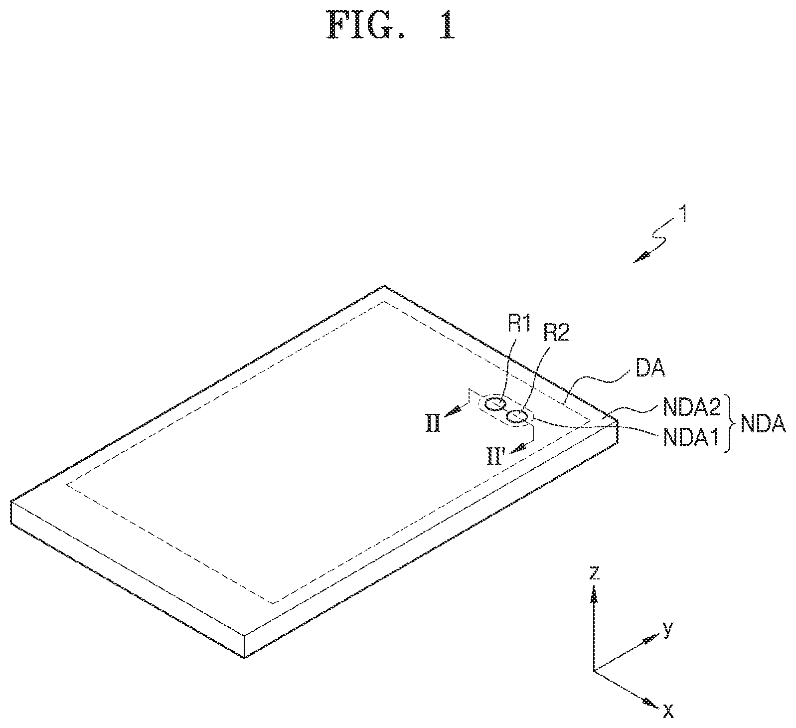
is a schematic perspective view of a display device 1 according to an embodiment.
Referring to , the display device 1 includes a display area DA that may emit light and a non-display area NDA that does not emit light.
The display device 1 may provide an image through the display area DA. The display device 1 may include a liquid crystal display (LCD), an electrophoretic display, an organic light-emitting display, an inorganic light-emitting display, a quantum-dot light emitting display, a field emission display, a surface-conduction electron-emitter display, a plasma display, or a cathode ray display.
The display device 1 may be an organic light-emitting display according to an embodiment.
The display device 1 includes a first region R 1 and a second region R 2 . In/on the first region R 1 and the second region R 2 , electronic elements are arranged. The first and second regions R 1 and R 2 may be/include openings (e.g., cavities or through holes) and/or transmission areas capable of transmitting light or/and sound from or to the electronic elements. One, two, three, or more openings and/or transmission areas may be included in the display device 1 .
According to an embodiment, at the first region R 1 and the second region R 2 , a light transmittance may be about 30% or greater, 50% or greater, 70% or greater, 80% or greater, or 85% or greater.
The non-display area NDA may include a first non-display area NDA 1 surrounding the regions R 1 and R 2 and may include a second non-display area NDA 2 surrounding the display area DA. The first non-display area NDA 1 may entirely surround the first and second regions R 1 and R 2 , the display area DA may entirely surround the first non-display area NDA 1 , and the second non-display area NDA 2 may entirely surround the display area DA.
The regions R 1 and R 2 are positioned on the upper right side of the display area DA in . According to an embodiment, locations of the first region R 1 and the second region R 2 may be different from those illustrated in .
A to 2 C each illustrate a schematic cross-sectional view of the display device 1 taken along line II-II′ of according to an embodiments.
Referring to A , the display device 1 may include a display panel 10 and electronic elements 20 and 30 respectively corresponding to the regions R 1 and R 2 of the display panel 10 . Although not shown, one or more components, such as an input sensing member for sensing a touch input, an anti-reflection member including a polarizer and a retarder, or a color filter and a black matrix, and a transparent window, may be arranged on/in the display panel 10 .
The display panel 10 may include a substrate 100 , an encapsulation substrate 400 A that faces the substrate 100 , and a sealing member 450 between the substrate 100 and the encapsulation substrate 400 A.
The substrate 100 may include glass or polymer resin. Examples of the polymer resin may include polyethersulphone (PES), polyacrylate (PAR), polyetherimide (PEI), polyethylene naphthalate (PEN), polyethylene terephthalate (PET), polyphenylene sulfide (PPS), polyarylate, polyimide (PI), polycarbonate (PC), and cellulose acetate propionate (CAP). The substrate 100 including polymer resin may be flexible, rollable, or bendable. The substrate 100 may have a multi-layered structure including a polymer resin layer and an inorganic layer (not shown). The encapsulation substrate 400 A may include glass or polymer resin.
A thin-film transistor TFT, an organic light-emitting diode OLED connected to the thin-film transistor TFT, and signal lines SGL are arranged on the display area DA of the substrate 100 (which corresponds to the display area DA of the display device 1 ). Signal lines SGL and a dummy thin-film transistor TFT′ are arranged on the first non-display area NDA 1 of the substrate 100 .
Signal lines SGL may provide certain signals (e.g., a data signal and a scan signal) to display elements spaced apart from each other in a y direction about the regions R 1 and R 2 .
The display panel 10 may include through holes corresponding to the regions R 1 and R 2 . For example, the substrate 100 and the encapsulation substrate 400 A may include through holes 100 H and through holes 400 AH, respectively, wherein the through holes 100 H correspond to the regions R 1 and R 2 and the through holes 400 AH correspond to the regions R 1 and R 2 . Portions of an insulating layer IL or elements between the substrate 100 and the encapsulation substrate 400 A that correspond to the regions R 1 and R 2 may be all removed.
A illustrates that sealing members 450 are arranged on opposite sides of each of the regions R 1 and R 2 . When viewed in a direction perpendicular to a main surface of the substrate 100 , i.e., in a plan view of the display panel 10 , each of the regions R 1 and R 2 may be entirely surrounded by the sealing members 450 .
The electronic elements 20 and 30 may be located in the regions R 1 and R 2 , respectively. The electronic elements 20 and 30 may be electronic elements that use, input, and/or output light or sound. For example, an electronic element may be a sensor that receives and uses light (like an infrared sensor), a camera that receives light and captures an image, a sensor that outputs and senses light or sound to measure a distance or recognize a fingerprint, a small lamp that outputs light, or a speaker that outputs sound. An electronic element using light may use light in one or more of various wavelength bands, such as visible light, infrared light, and/or ultraviolet light.
Since the display panel 10 includes through holes corresponding to the regions R 1 and R 2 , as in A , light or sound may be effectively output or received by the electronic elements 20 .
Some elements of the display panel 10 may not include through holes that correspond to the regions R 1 and R 2 . For example, as illustrated in B , the encapsulation substrate 400 A may include through holes 400 AH corresponding to the regions R 1 and R 2 but the substrate 100 may include no through holes. Alternatively, as illustrated in C , both the encapsulation substrate 400 A and the substrate 100 may not include through holes corresponding to the regions R 1 and R 2 . As illustrated in B and 2 C , even though the substrate 100 does not include the through hole 100 H, the insulating layer IL and/or elements between the substrate 100 and the encapsulation substrate 400 A may include cavities that correspond to the regions R 1 and R 2 , and thus sufficient light transmittance may be provided for operations of the electronic elements 20 and 30 . When the display device 1 includes any of the display panels 10 of B and 2 C , the electronic elements 20 and 30 may be electronic elements that use light.
A to 3 C each illustrate a schematic cross-sectional view of the display device 1 taken along line II-II′ of according to an embodiment.
Similar to the display device 1 described above with reference to A , the display device 1 of A may include a display panel 10 including a display element, and electronic elements 20 and 30 respectively corresponding to regions R 1 and R 2 of the display panel 10 . Although not shown, the display device 1 may further include an input detection member for sensing a touch input, a reflection prevention member, a window, etc. arranged on the display panel 10 .
The display panel 10 may include a thin-film encapsulation layer 400 B, for enhancing flexibility.
The thin-film encapsulation layer 400 B may include at least one inorganic encapsulation layer and at least one organic encapsulation layer. A illustrates inorganic encapsulation layers 410 and 430 and an intervening organic encapsulation layer 420 .
The inorganic encapsulation layers 410 and 430 may include at least one inorganic insulating material, such as aluminum oxide, titanium oxide, tantalum oxide, hafnium oxide, zinc oxide, silicon oxide, silicon nitride, and/or silicon oxynitride. The organic encapsulation layer 420 may include a polymer-based material. Examples of the polymer-based material may include acrylic resin, epoxy resin, polyimide, and polyethylene.
The display panel 10 may include through holes corresponding to the regions R 1 and R 2 . For example, the substrate 100 and the thin-film encapsulation layer 400 B may include through holes 100 H and through holes 400 BH, respectively. The electronic elements 20 and 30 using light or sound may be arranged in the regions R 1 and R 2 , respectively.
As illustrated in B , the thin-film encapsulation layer 400 B may include the through holes 400 BH corresponding to the regions R 1 and R 2 , but the substrate 100 may include no through holes. Alternatively, as illustrated in C , both the thin-film encapsulation layer 400 B and the substrate 100 may not include through holes corresponding to the regions R 1 and R 2 . As illustrated in B and 3 C , even though the substrate 100 does not include the through holes 100 H, an insulating layer IL and/or elements between the substrate 100 and the thin-film encapsulation layer 400 B may include through holes and/or cavities that correspond to the regions R 1 and R 2 , thus sufficient light transmittance may be enabled for operations of the electronic elements 20 and 30 .
When the thin-film encapsulation layer 400 B includes the through holes 400 BH as shown in A and 3 B , each of the at least one inorganic encapsulation layer and the at least one organic encapsulation layer may include holes corresponding to the through holes 400 BH. In this case, the holes of each organic encapsulation layer are made larger than those of each inorganic encapsulation layer, and thus the inorganic encapsulation layers 410 and 430 may directly contact each other around the regions R 1 and R 2 .
When the thin-film encapsulation layer 400 B includes no through holes as shown in C , each of the at least one inorganic encapsulation layer and the at least one organic encapsulation layer may cover the regions R 1 and R 2 . The insulating layer IL between the substrate 100 and the thin-film encapsulation layer 400 B may include through holes and/or cavities. Portions of the insulating layer IL that correspond to the regions R 1 and R 2 are completely removed in A . In an embodiment, only portions of some of multiple layers that constitute the insulating layer IL may be removed.
is a schematic plan view of a display panel 10 according to an embodiment, and A and 5 B each illustrate a plan view of a region III of according to an embodiment.
Referring to and A or B , the display panel 10 includes a plurality of pixels P arranged in the display area DA. Each of the pixels P may include a display element, such as an organic light-emitting diode. The pixel PX may emit, for example, red light, green light, blue light, or white light using the organic light-emitting diode. The display area DA may be protected against external air or moisture by an encapsulation member described above with reference to A to 3 C .
The first non-display area NDA 1 surrounds the regions R 1 and R 2 . The first non-display area NDA 1 is not for displaying images. Signal lines that provide signals to the pixels P around the regions R 1 and R 2 may be arranged in the first non-display area NDA 1 . Dummy pixels Pd that do not emit light are arranged in the first non-display area NDA 1 .
The second non-display area NDA 2 may include a scan driver 1000 that provides scan signals to the pixels P and the dummy pixels Pd, a data driver 2000 that provides data signals to the pixels P and the dummy pixels Pd, and a main power line (not shown) for providing a driving voltage and a common voltage.
A and 5 B are plan views of the region III of .
Referring to A and 5 B , the first region R 1 and the second region R 2 are arranged (and aligned) in a first direction, the first non-display area NDA 1 surrounds the first region R 1 and the second region R 2 , and the display area DA surrounds the first non-display area NDA 1 .
Pixels P are arranged in the display area DA, and dummy pixels Pd are arranged in the first non-display area NDA 1 . A plurality of signal lines may electrically connect the pixels P to the dummy pixels Pd. A illustrates that scan lines SLa and SLb, each extending substantially in the first direction (x direction), connect pixels P in the display area DA to dummy pixels Pd in the first non-display area NDA 1 and illustrates that (data line DLa and) data line DLb may electrically connect pixels P to dummy pixels Pd substantially in a second direction (y direction) may intersect the scan lines SLa and SLb.
Some scan lines SLa may each extend substantially in the first direction (x direction) to provide signals to the pixels P positioned on opposite sides (e.g., the left and right sides) of the first non-display area NDA 1 and to the dummy pixels Pd positioned in the first non-display area NDA 1 , but may bypass (or detour around) the first region R 1 and the second region R 2 in the first non-display area NDA 1 . Some scan lines SLb arranged sufficiently far from the first region R 1 and the second region R 2 in the first non-display area NDA 1 or scan lines that do not traverse the first non-display area NDA 1 may each extend in a substantially straight line.
Some data lines DLa may each extend substantially in the second direction (y direction) to provide signals to the pixels P arranged on opposite sides (e.g., the upper and lower sides) of the first non-display area NDA 1 , but may bypass (or detour around) the first region R 1 and the second region R 2 in the first non-display area NDA 1 . Some data lines DLb arranged between the first region R 1 and the second region R 2 in the first non-display area NDA 1 or data lines that do not traverse the first non-display area NDA 1 may each extend in a substantially straight line.
For example, when the first region R 1 and the second region R 2 have circular shapes, signal lines positioned close to the first region R 1 and the second region R 2 may curve along the first region R 1 and the second region R 2 , and signal lines positioned far from the first region R 1 and the second region R 2 may each extend in a straight line.
The dummy pixels Pd positioned in the first non-display area NDA 1 may include no light emitting elements and may emit no light even when they receive electrical signals from signal lines.
The dummy pixels Pd may be included to secure uniformity of a pattern density and uniformity of an electrical load. If no dummy pixels Pd are arranged in the first non-display area NDA 1 and if only signal lines SLa, SLb, DLa, and DLb (connecting pixels P in the display area DA to each other) are arranged in the first non-display area NDA 1 , a pattern density is low in the first non-display area NDA 1 ; as a result, a non-uniform pattern may be undesirably formed during etching.
Moreover, if no dummy pixels Pd are arranged in the first non-display area NDA 1 , a parasitic capacitance or a different load in the first non-display area NDA 1 and its surroundings may be substantially different from that in a center portion of the display area DA. Accordingly, brightness of a displayed image may be undesirably non-uniform.
According to an embodiment, the first non-display area NDA 1 includes a dummy pixel circuit PC′ having substantially the same structure as a pixel circuit PC (see A ) included in each pixel P, and an electrical signal is applied to the dummy pixel circuit PC′; thus, uniformity of a pattern density and uniformity of an electrical load may be both secured.
Dummy pixels Pd may be positioned in the first non-display area NDA 1 between the first region R 1 and the second region P 2 .
As shown in B , dummy pixels Pd may surround the first region R 1 and/or the second region R 2 . Dummy pixels Pd may be between the first region R 1 and the second region R 2 and may be on the left, upper, and lower sides of the first region R 1 and close to the display area DA. Dummy pixels Pd may be on the right, upper, and lower sides of the second region R 2 and close to the display area DA.
Dummy pixels Pd may be arranged between pixels P and the first region R 1 and/or between pixels P and the second region R 2 . The dummy pixels Pd may protect the pixels P (in the display area DA) from electrostatic discharge (ESD) that may occur around the first region R 1 and/or the second region R 2 . The dummy pixels Pd may serve as a buffer to prevent a large voltage caused by ESD from being transmitted to the pixels P.
A to 6 D each illustrate a schematic cross-sectional view of a pixel P and a dummy pixel Pd taken along lines C-C′ and B-B′ of A or B according to an embodiment.
Referring to A , the pixel P may include a pixel circuit PC including at least one thin-film transistor TFT and may include an organic light-emitting diode OLED as a display element. The dummy pixel Pd may include a dummy pixel circuit PC′ including at least one dummy thin-film transistor TFT′. The pixel circuit PC and the dummy pixel circuit PC′ may have the same structure.
In the dummy pixel Pd, some components of a display element are removed or not provided such that light is not emitted even when an electrical signal is applied to the dummy pixel circuit PC′.
Compared with the pixel P, no pixel electrode 310 is arranged in the dummy pixel Pd, and thus light is not emitted. The dummy pixel Pd may not include an opposite electrode 330 of the organic light-emitting diode OLED. Various modifications may be made.
Although a single thin-film transistor TFT is included in the pixel circuit PC and a single thin-film transistor TFT′ is included in the dummy pixel circuit PC′ in A , a plurality of (e.g., two to seven) thin-film transistors TFT and a plurality of (e.g., two to seven) thin-film transistors TFT′ may be included. Various modifications may be made.
The substrate 100 may include a glass material, a metal material, or a material that is flexible or bendable. When the substrate 100 is flexible or bendable, the substrate 100 may include a polymer resin, such as polyethersulphone (PES), polyacrylate (PAR), polyetherimide (PEI), polyethylene naphthalate (PEN), polyethylene terephthalate (PET), polyphenylene sulfide (PPS), polyarylate, polyimide (PI), polycarbonate (PC), or cellulose acetate propionate (CAP). The substrate 100 may have a structure of a single layer or multiple layers. The multi-layered structure may include an inorganic layer. In some embodiments, the substrate 100 may have a structure of stacked organic material, inorganic material, and organic material.
A buffer layer 111 may be positioned on the substrate 100 and may reduce or prevent infiltration of a foreign material, moisture, or ambient air from the substrate 100 to the circuits PC and PC′ and may provide a flat surface on the substrate 100 . The buffer layer 111 may include an inorganic material (such as oxide or nitride), an organic material, or an organic and inorganic composite/combination, and may be include a single layer or multiple layers of an inorganic material and an organic material.
A barrier layer (not shown) may be further included between the substrate 100 and the buffer layer 111 . The barrier layer may prevent or minimize infiltration of impurities from the substrate 100 and the like into semiconductor layers A and A′. The barrier layer may include an inorganic material (such as oxide or nitride), an organic material, or an organic and inorganic combination/composite, and may be formed as a single layer or multiple layers of an inorganic material and an organic material.
The semiconductor layers A and A′ may be arranged on the buffer layer 111 . The semiconductor layers A and A′ may include amorphous silicon or polysilicon. According to an embodiment, the semiconductor layers A and A′ may include oxide of at least one selected from the group consisting of indium (In), gallium (Ga), tin (Sn), zirconium (Zr), vanadium (V), hafnium (Hf), cadmium (Cd), germanium (Ge), chromium (Cr), titanium (Ti), aluminum (Al), cesium (Cs), cerium (Ce), and zinc (Zn). In some embodiments, the semiconductor layers A and A′ may be formed of Zn oxide, In—Zn oxide, Ga—In—Zn oxide, or the like as a Zn oxide-based material. In embodiments, the semiconductor layers A and A′ may be an In—Ga—Zn—O (IGZO), In—Sn—Zn—O (ITZO), or In—Ga—Sn—Zn—O (IGTZO) semiconductor containing a metal, such as In, Ga, or Sn, in ZnO. The semiconductor layers A and A′ each may include a channel region, and a source region and a drain region respectively arranged on two sides of the channel region. Each of the semiconductor layers A and A′ may be a single layer or multiple layers.
Gate electrodes G and G′ are arranged on the semiconductor layers A and A′ with an intervening first gate insulating layer 112 ; the gate electrodes G and G′ at least partially overlap the semiconductor layers A and A′. The gate electrodes G and G′ may include, for example, molybdenum (Mo), aluminum (Al), copper (Cu), or titanium (Ti), and each may include a single layer or multiple layers. For example, each of the gate electrodes G and G′ may include a single layer of Mo.
The first gate insulating layer 112 may include silicon oxide (SiO 2 ), silicon nitride (SiNx), silicon oxynitride (SiON), aluminum oxide (Al 2 O 3 ), titanium oxide (TiO 2 ), tantalum oxide (Ta 2 O 5 ), hafnium oxide (HfO 2 ), zinc oxide (ZnO 2 ), or the like.
A second gate insulating layer 113 may cover the gate electrodes G and G′. The second gate insulating layer 113 may include silicon oxide (SiO 2 ), silicon nitride (SiNx), silicon oxynitride (SiON), aluminum oxide (Al 2 O 3 ), titanium oxide (TiO 2 ), tantalum oxide (Ta 2 O 5 ), hafnium oxide (HfO 2 ), zinc oxide (ZnO 2 ), or the like.
First storage capacitor plates CE 1 and CE 1 ′ of storage capacitors Cst and Cst′ may overlap the thin-film transistors TFT and TFT′. The gate electrodes G and G′ of the thin-film transistors TFT and TFT′ may function as the first storage capacitor plates CE 1 and CE 1 ′ of the storage capacitors Cst and Cst′.
Second storage capacitor plates CE 2 and CE 2 ′ of the storage capacitors Cst and Cst′ overlap the first storage capacitor plates CE 1 and CE 1 ′ with the intervening second gate insulating layer 113 . The second gate insulating layer 113 may function as dielectric layers of the storage capacitors Cst and Cst′. The second storage capacitor plates CE 2 and CE 2 ′ may include a conductive material including molybdenum (Mo), aluminum (Al), copper (Cu), and titanium (Ti), and each may be a multi-layer or single layer. For example, the second storage capacitor plates CE 2 and CE 2 ′ may each include a single layer of Mo or a multi-layer structure of Mo—Al—Mo.
The storage capacitors Cst and Cst′ overlap the thin-film transistors TFT and TFT′ in A to 6 D . In an embodiment, the storage capacitors Cst and Cst′ may not overlap the thin-film transistors TFT and TFT′.
An interlayer insulating layer 115 may cover the second storage capacitor plates CE 2 and CE 2 ′ of the storage capacitors Cst and Cst′. The interlayer insulating layer 115 may include silicon oxide (SiO 2 ), silicon nitride (SiNx), silicon oxynitride (SiON), aluminum oxide (Al 2 O 3 ), titanium oxide (TiO 2 ), tantalum oxide (Ta 2 O 5 ), hafnium oxide (HfO 2 ), zinc oxide (ZnO 2 ), or the like.
Source electrodes S and S′ and drain electrodes D and D′ may be arranged on the interlayer insulating layer 115 . Each of the source electrode S and S′ and the drain electrodes D and D′ may include a conductive material including Mo, Al, Cu, and Ti, and may be a multi-layer structure or single layer. For example, each of the source electrodes S and S′ and the drain electrodes D and D′ may be a multi-layer structure of Ti—Al—Ti.
A via layer 117 and an additional via layer 118 may be positioned on the source electrodes S and S′ and the drain electrodes D and D′, and the organic light-emitting diode OLED may be positioned in a region of the pixel P on the additional via layer 118 . In some embodiments, the additional via layer 118 may be unnecessary.
The via layer 117 and the additional via layer 118 may have flat upper surfaces such that the pixel electrode 310 may be sufficiently flat. The via layer 117 and the additional via layer 118 may each be a single layer including an organic material or multiple layers including an organic material. The via layer 117 and the additional via layer 118 may include a polymer such as benzocyclobutene (BCB), polyimide, hexamethyldisiloxane (HMDSO), polymethyl methacrylate (PMMA) or polystyrene (PS), a polymer derivative having a phenol-based group, an acryl-based polymer, an imide-based polymer, an acryl ether-based polymer, an amide-based polymer, a fluorine-based polymer, a p-xylene-based polymer, a vinyl alcohol-based polymer, a blend thereof, or the like. The via layer 117 and the additional via layer 118 may include an inorganic material. The via layer 117 and the additional via layer 118 may include silicon oxide (SiO 2 ), silicon nitride (SiNx), silicon oxynitride (SiON), aluminum oxide (Al 2 O 3 ), titanium oxide (TiO 2 ), tantalum oxide (Ta 2 O 5 ), hafnium oxide (HfO 2 ), zinc oxide (ZnO 2 ), or the like. When the via layer 117 and the additional via layer 118 include an inorganic material, chemical planarization polishing may be conducted. The via layer 117 may include both an organic material and an inorganic material.
On the display area DA of the substrate 100 , the organic light-emitting diode OLED is positioned on the additional via layer 118 . The organic light-emitting diode OLED includes the pixel electrode 310 , the opposite electrode 330 , and an intermediate layer 320 including an organic emission layer.
A via hole via is positioned in the via layer 117 and the additional via layer 118 and may expose one of the source electrode S and the drain electrode D of the thin-film transistor TFT, and the pixel electrode 310 contacts the source electrode S or the drain electrode D via the via hole and is electrically connected to the thin-film transistor TFT.
The pixel electrode 310 may be a transparent electrode, a semi-light-transmissive electrode, or a reflective electrode. The pixel electrode 310 may include a reflection layer formed of silver (Ag), magnesium (Mg), aluminum (Al), platinum (Pt), palladium (Pd), gold (Au), nickel (Ni), neodymium (Nd), iridium (Ir), chromium (Cr), or a combination/alloy, and may include a transparent or semi-transparent electrode layer formed on the reflection layer. The transparent or semi-transparent electrode layer may include at least one selected from the group consisting of indium tin oxide (ITO), indium zinc oxide (IZO), zinc oxide (ZnO), indium oxide (In 2 O 3 ), indium gallium oxide (IGO), and aluminum zinc oxide (AZO). The pixel electrode 310 may have a stack structure of ITO—Ag-ITO.
A pixel defining layer 119 may be disposed on the additional via layer 118 . The pixel defining layer 119 may define light-emission regions of pixels P at openings OP respectively corresponding to the pixel electrodes 310 . The openings OP may expose at least center portions of the pixel electrodes 310 . The pixel defining layer 119 may prevent an electric arc from occurring on the edges of the pixel electrodes 310 by increasing distances between the edges of the pixel electrodes 310 and the opposite electrodes 330 . The pixel defining layer 119 may be formed of an organic insulating material, such as polyimide, polyamide, acryl resin, benzocyclobutene, hexamethyldisiloxane (HMDSO), or phenol resin, via spin coating or the like.
The light-emission regions of the pixels P may be defined by the openings OP of the pixel defining layer 119 . Edges of the pixels P may correspond to edges of the openings OP of the pixel defining layer 119 . The edges of the openings OP of the pixel defining layer 119 may correspond to boundaries of portions of the pixel electrodes 310 that are exposed via the openings OP.
The intermediate layer 320 of the organic light-emitting diode OLED may include an organic emission layer 321 , and a first common layer 322 and a second common layer 323 that may be respectively disposed on opposite faces (e.g., the bottom and top) of the organic emission layer 321 .
The organic emission layer 321 may include an organic material including a fluorescent or phosphorescent material that may emit red, green, blue, or white light. The organic emission layer 321 may include a low-molecular weight organic material or a high-molecular weight organic material.
The first common layer 322 may include a hole injection layer (HIL) and/or a hole transport layer (HTL), and the second common layer 323 may include an electron transport layer (ETL) and/or an electron injection layer (EIL).
An intermediate layer 320 may correspond to each of a pixel electrode 310 . The first common layer 322 and/or the second common layer 323 may extend over pixel electrodes 310 . The first common layer 322 and/or the second common layer 323 may be unnecessary.
The opposite electrode 330 may include a light-transmissive electrode or a reflective electrode. According to some embodiment, the opposite electrode 330 may include a transparent or semi-transparent electrode, and may include a metal thin film having a small/low work function, including lithium (Li), calcium (Ca), lithium fluoride/calcium (LiF/Ca), lithium fluoride/aluminum (LiF/Al), aluminum (Al), silver (Ag), magnesium (Mg), or a combination/alloy. A transparent conductive oxide (TCO) layer including TCO, such as indium tin oxide (ITO), indium zinc oxide (IZO), zinc oxide (ZnO), or indium oxide (In 2 O 3 ), may be disposed on the metal thin film. The opposite electrode 330 may extend over both the display area DA and the non-display area NDA and may be arranged on the intermediate layer 320 and the pixel defining layer 119 . Portions of the opposite electrode 330 may be parts of a plurality of organic light-emitting diodes OLED and may correspond to a plurality of pixel electrodes 310 .
When the pixel electrode 310 includes a reflective electrode and the opposite electrode 330 includes a light-transmissive electrode, light emitted by the intermediate layer 320 is emitted toward the opposite electrode 330 , and the display device 1 may be of a top-emission type. When the pixel electrode 310 includes a transparent or semi-transparent electrode and the opposite electrode 330 includes a reflective electrode, light emitted by the intermediate layer 320 is emitted toward the substrate 100 , and the display device 1 may be of a bottom-emission type. The display device 1 may emit light toward both the top surface and the bottom surface of the display device 1 .
A dummy pixel Pd arranged in the first non-display area NDA 1 of the substrate 100 may include no pixel electrode, and the pixel defining layer 119 may not include an opening corresponding to the dummy pixel Pd. The pixel defining layer 119 may have a flat upper surface at the dummy pixel Pd. The pixel defining layer 119 may be formed of an organic material (via exposure and curing) and may not affect non-uniformity or pattern density.
At the dummy pixel Pd, the intermediate layer 320 may be positioned on the pixel defining layer 119 . Even when the intermediate layer 320 is arranged in the region of the dummy pixel Pd, the dummy pixel Pd includes no pixel electrodes, and thus no light is emitted by the intermediate layer 320 .
In A , the organic emission layer 321 , the first common layer 322 , and the second common layer 323 are all arranged in the region of the dummy pixel Pd, like the intermediate layer 320 arranged in the pixel P.
In B , the organic emission layer 321 , the first common layer 322 , and the second common layer 323 may be arranged at the pixel P; at the dummy pixel Pd, no organic emission layers 321 may be arranged, and only the first common layer 322 and the second common layer 323 may be arranged. The common layers 322 and 323 may directly contact each other at the dummy pixel Pd.
In C , the intermediate layer 320 may be arranged at the pixel P, and no intermediate layers 320 may be arranged at the dummy pixel Pd. The opposite electrodes 330 may directly contact an upper surface of the pixel defining layer 119 at the dummy pixel Pd.
In D , the opposite electrode 330 may not be arranged in the dummy pixel Pd. A the dummy pixel Pd, a conductive layer 310 ′ including the same material as that included in the pixel electrode 310 and positioned on the same layer on which the pixel electrode 310 is formed. The organic emission layer 321 , the first common layer 322 , and the second common layer 323 of the intermediate layer 320 may be arranged in the dummy pixel Pd. At least one of the conductive layer 310 ′, the organic emission layer 321 , the first common layer 322 , and the second common layer 323 may not be formed at the dummy pixel Pd.
Because the opposite electrode 330 is formed over the entire display panel using an open mask, the opposite electrode 330 may correspond to the pixel P and the dummy pixel Pd.
A capping layer 340 may be arranged on the opposite electrode 330 . The capping layer 340 may have a different (lower or higher) refractive index than the opposite electrode 330 and may improve luminescent efficiency by increasing a percentage that light generated by the intermediate layer 320 is totally reflected and is emitted outside the display panel 10 .
The capping layer 340 may include an organic material, such as at least one of poly(3,4-ethylenedioxythiophene) (or PEDOT), 4,4′-bis [N-(3-methylphenyl)-N-phenylamino] biphenyl (TPD), 4,4′,4″-tris [(3-methylphenyl) phenylamino] triphenylamine (m-MTDATA), 1,3,5-tris [N,N-bis(2-methylphenyl)-amino]-benzene (o-MTDAB), 1,3,5-tris [N, N-bis (3-methylphenyl)-amino]-benzene (m-MTDAT), 1,3,5-tris [N,N-bis (4-methylphenyl)-amino]-benzene (p-MTDAB), 4,4′-bis [N, N-bis (3-methylphenyl)-amino]-diphenylmethane (BPPM), 4,4′-dicarbazolyl-1,1′-biphenyl (CBP), 4,4′,4″-tris (N-carbazole) triphenylamine (TCTA), 2,2′,2″-(1,3,5-benzenetolyl) tris-[1-phenyl-1H-benzoimidazole] (TPBI), and 3-(4-biphenyl)-4-phenyl-5-t-butylphenyl-1,2,4-triazole (TAZ).
The capping layer 340 may include an inorganic material, such as at least one of zinc oxide, titanium oxide, zirconium oxide, silicon nitride, niobium oxide, tantalum oxide, tin oxide, nickel oxide, indium nitride, and gallium nitride.
A cover layer (not shown) may be arranged on the capping layer 340 . The cover layer protects the organic light-emitting diode OLED against damage that may occur during a subsequent process using plasma or the like. The cover layer may include LiF.
A and 7 B are schematic equivalent circuit diagrams of a pixel P of a display panel according to embodiments.
Referring to A , each pixel P includes a pixel circuit PC and an organic light-emitting diode OLED connected to the pixel circuit PC. The pixel circuit PC may include a driving thin-film transistor (TFT) T 1 , a switching TFT T 2 , and a storage capacitor Cst.
The switching TFT T 2 is connected to a scan line SL and a data line DL, and transmits, to the driving TFT T 1 , a data voltage received via the data line DL according to a switching voltage received via the scan line SL. The storage capacitor Cst is connected to the switching TFT T 2 and a driving voltage line PL, and stores a voltage corresponding to a difference between a voltage received from the switching TFT T 2 and a driving voltage ELVDD supplied to the driving voltage line PL.
The driving TFT T 1 is connected to the driving voltage line PL and the storage capacitor Cst, and may control a driving current flowing from the driving voltage line PL to the organic light-emitting diode OLED, in accordance with a voltage value stored in the storage capacitor Cst. The organic light-emitting diode OLED may emit light having a certain brightness according to the driving current. An opposite electrode (for example, a cathode) of the organic light-emitting diode OLED may receive a common voltage ELVSS.
Although a case where the pixel circuit PC includes two TFTs and one storage capacitor is illustrated in A , the disclosure is not limited thereto. The number of TFTs and the number of storage capacitors may vary according to a design of the pixel circuit PC.
Referring to B , the pixel circuit PC may include a plurality of TFTs and a storage capacitor Cst. The TFTs and the storage capacitor may be connected to signal lines SL, SIL, EL, and DL, an initializing voltage line VL, and a driving voltage line PL.
Although each pixel P is connected to the signal lines SL, SIL, EL, and DL, the initializing voltage line VL, and the driving voltage line PL in B , the disclosure is not limited thereto. According to another embodiment, the initializing voltage line VL, the driving voltage line PL, and at least one of the signal lines SL, SIL, EL, and DL may be shared by neighboring pixels.
The plurality of TFTs may include a driving TFT T 1 , a switching TFT T 2 , a compensating TFT T 3 , a first initializing TFT T 4 , an operation control TFT T 5 , a light-emission control TFT T 6 , and a second initializing TFT T 7 .
The signal lines SL, SIL, EL, and DL may include a scan line SL that transmits a scan signal SL, a previous scan line SIL that transmits a previous scan signal SIL to the second initializing TFT T 7 , a light-emission control line EL that transmits a light-emission control signal En to the operation control TFT T 5 and the light-emission control TFT T 6 , and a data line DL that intersects with the scan line SL and transmits a data signal Dm. The driving voltage line PL transmits a driving voltage ELVDD to the driving TFT T 1 , and the initializing voltage line VL transmits an initializing voltage Vint that initiates the driving TFT T 1 and a pixel electrode of the organic light-emitting diode OLED.
The driving TFT T 1 includes a driving gate electrode G 1 connected to a first storage capacitor plate CE 1 of the storage capacitor Cst, a driving source electrode S 1 connected to the driving voltage line PL via the operation control TFT T 5 , and a driving drain electrode D 1 electrically connected to the pixel electrode of the organic light-emitting diode OLED via the light-emission control TFT T 6 . The driving TFT T 1 receives the data signal Dm according to a switching operation of the switching TFT T 2 and supplies a driving current I OLED to the organic light-emitting diode OLED.
The switching TFT T 2 includes a switching gate electrode G 2 connected to the scan line SL, a switching source electrode S 2 connected to the data line DL, and a switching drain electrode D 2 connected to the driving source electrode S 1 of the driving TFT T 1 and also connected to the driving voltage line PL via the operation control TFT T 5 . The switching TFT T 2 is turned on according to the scan signal GW received via the scan line SL and performs a switching operation of transmitting the data signal Dm received from the data line DL to the driving source electrode S 1 of the driving TFT T 1 .
The compensating TFT T 3 includes a compensating gate electrode G 3 connected to the scan line SL, a compensating source electrode S 3 connected to the driving drain electrode D 1 of the driving TFT T 1 and also connected to the pixel electrode of the organic light-emitting diode OLED via the light-emission control TFT T 6 , and a compensating drain electrode D 3 connected to the first storage capacitor plate CE 1 of the storage capacitor Cst, a first initializing drain electrode D 4 of the first initializing TFT T 4 , and the driving gate electrode G 1 of the driving TFT T 1 . The compensating TFT T 3 is turned on according to the scan signal GW received via the scan line SL and electrically connects the driving gate electrode S 1 and the driving drain electrode D 1 of the driving TFT T 1 to each other, such that the driving TFT T 1 is diode-connected.
The first initializing TFT T 4 includes a first initializing gate electrode G 4 connected to the previous scan line SIL, a first initializing source electrode S 4 connected to a second initializing drain electrode D 7 of the second initializing TFT T 7 and the initializing voltage line VL, and the first initializing drain electrode D 4 connected to the first storage capacitor plate CE 1 of the storage capacitor Cst, the compensating drain electrode D 3 of the compensating TFT T 3 , and the driving gate electrode G 1 of the driving TFT T 1 . The first initializing TFT T 4 is turned on according to the previous scan signal SI received via the previous scan line SIL and transmits the initializing voltage Vint to the driving gate electrode G 1 of the driving TFT T 1 to thereby initialize a voltage of the driving gate electrode G 1 of the driving TFT T 1 .
The operation control TFT T 5 includes an operation control gate electrode G 5 connected to the light-emission control line EL, an operation control source electrode S 5 connected to the driving voltage line PL, and an operation control drain electrode D 5 connected to the driving source electrode S 1 of the driving TFT T 1 and the switching drain electrode D 2 of the switching TFT T 2 .
The light-emission control TFT T 6 includes a light-emission control gate electrode G 6 connected to the light-emission control line EL, a light-emission control source electrode S 6 connected to the driving drain electrode D 1 of the driving TFT T 1 and the compensating source electrode S 3 of the compensating TFT T 3 , and a light-emission control drain electrode D 6 electrically connected to a second initializing source electrode S 7 of the second initializing TFT T 7 and the pixel electrode of the organic light-emitting diode OLED.
The operation control TFT T 5 and the light-emission control TFT T 6 are simultaneously turned on according to the light-emission control signal EM received via the light-emission control line EL, and thus the driving voltage ELVDD is transmitted to the organic light-emitting diode OLED such that the driving current I OLED may flow in the organic light-emitting diode OLED.
The second initializing TFT T 7 includes a second initializing gate electrode G 7 connected to the previous scan line SIL, the second initializing source electrode S 7 connected to the light-emission control drain electrode D 6 of the light-emission control TFT T 6 and the pixel electrode of the organic light-emitting diode OLED, and the second initializing drain electrode D 7 connected to the first initializing source electrode S 4 of the first initializing TFT T 4 and the initializing voltage line VL. The second initializing TFT T 7 is turned on according to the previous scan signal Sn−1 received via the previous scan line SIL and initializes the pixel electrode of the organic light-emitting diode OLED.
Although the first initializing TFT T 4 and the second initializing TFT T 7 are connected to the previous scan line SIL in B , the disclosure is not limited thereto. According to another embodiment, the first initializing TFT T 4 may be connected to the previous scan line SIL and operate according to the previous scan signal Sn−1, and the second initializing TFT T 7 may be connected to a separate signal line (for example, a subsequent scan line) and operate according to a signal transmitted to the separate signal line.
A second storage capacitor plate CE 2 of the storage capacitor Cst is connected to the driving voltage line PL, and an opposite electrode of the organic light-emitting diode OLED is connected to a common voltage ELVSS. Accordingly, the organic light-emitting diode OLED may receive the driving current I OLED from the driving TFT T 1 and emit light, thereby displaying an image.
Although each of the compensating TFT T 3 and the first initializing TFT T 4 has a dual gate electrode in B , each of the compensating TFT T 3 and the first initializing TFT T 4 may have a single gate electrode.
The pixel circuit PC included in the pixel P illustrated in A and 7 B is applicable to the dummy pixel circuit PC′ included in the dummy pixel Pd.
is a plan view of a pixel circuit applicable to a display panel according to an embodiment. According to the present embodiments, a dummy pixel circuit may be the same as the pixel circuit. Thus, may be a plan view of a dummy pixel circuit applicable to a display panel according to an embodiment.
Referring to , the driving TFT T 1 , the switching TFT T 2 , the compensating TFT T 3 , the first initializing TFT T 4 , the operation control TFT T 5 , the light-emission control TFT T 6 , and the second initializing TFT T 7 are arranged along a semiconductor layer 1130 . The semiconductor layer 1130 may be arranged on a substrate on which a buffer layer including an inorganic insulating material is arranged.
Some regions of the semiconductor layer 1130 correspond to semiconductor layers of the driving TFT T 1 , the switching TFT T 2 , the compensating TFT T 3 , the first initializing TFT T 4 , the operation control TFT T 5 , the light-emission control TFT T 6 , and the second initializing TFT T 7 . In other words, it may be understood that the semiconductor layers of the driving TFT T 1 , the switching TFT T 2 , the compensating TFT T 3 , the first initializing TFT T 4 , the operation control TFT T 5 , the light-emission control TFT T 6 , and the second initializing TFT T 7 are connected to each other and bent in various shapes.
The semiconductor layer 1130 includes a channel region, and a source region and a drain region on two opposite sides of the channel region. The source region and the drain region may be understood as a source electrode and a drain electrode of the relevant TFT. Hereinafter, for convenience of description, the source region and the drain region are respectively called a source electrode and a drain electrode.
The driving TFT T 1 includes the driving gate electrode G 1 that overlaps a driving channel region, and the driving source electrode S 1 and the driving drain electrode D 1 on two opposite sides of the driving channel region. The driving channel region that overlaps the driving gate electrode G 1 may form a long channel within a narrow space by having a bent shape such as an omega shape. When the driving channel region is long, a driving range of a gate voltage is widened, and accordingly a gray scale of light emitted from the organic light-emitting diode OLED may be more elaborately controlled and display quality may be improved.
The switching TFT T 2 includes the switching gate electrode G 2 that overlaps a switching channel region, and the switching source electrode S 2 and the switching drain electrode D 2 on two opposite sides of the switching channel region. The switching drain electrode D 2 may be connected to the driving source electrode S 1 .
The compensating TFT T 3 is a dual TFT, and thus may include compensating gate electrodes G 3 that respectively overlap two compensating channel regions, and include the compensating source electrode S 3 and the compensating drain electrode D 3 arranged on two opposite sides of the compensating channel regions. The compensating TFT T 3 may be connected to the driving gate electrode G 1 of the driving TFT T 1 through a node connection line 1174 which will be described later.
The first initializing TFT T 4 is a dual TFT, and thus may include first initializing gate electrodes G 4 that respectively overlap two first initializing channel regions and include the first initializing source electrode S 4 and the first initializing drain electrode D 4 arranged on two opposite sides of the first initializing channel regions.
The operation control TFT T 5 may include the operation control gate electrode G 5 that overlaps an operation control channel region, and the operation control source electrode S 5 and the operation control drain electrode D 5 arranged on two opposite sides of the operation control channel region. The operation control drain electrode D 5 may be connected to the driving source electrode S 1 .
The light-emission control TFT T 6 may include the light-emission control gate electrode G 6 that overlaps a light-emission control channel region, and the light-emission control source electrode S 6 and the light-emission control drain electrode D 6 arranged on two opposite sides of the light-emission control channel region. The light-emission control source electrode S 6 may be connected to the driving drain electrode D 1 .
The second initializing TFT T 7 may include the second initializing gate electrode G 7 that overlaps a second initializing channel region, and the second initializing source electrode S 7 and the second initializing drain electrode D 7 arranged on two opposite sides of the second initializing channel region.
The aforementioned TFTs may be connected to the signal lines SL, SIL, EL, and DL, the initializing voltage line VL, and the driving voltage line PL.
The scan line SL, the previous scan line SIL, the light-emission control line EL, and the driving gate electrode G 1 may be arranged on the semiconductor layer 1130 with one or more intervening insulating layers.
The scan line SL may extend in the first direction. Some regions of the scan line SL may correspond to the switching and compensating gate electrodes G 4 and G 7 . For example, regions of the scan line SL that overlap the respective channel regions of the initializing TFTs T 4 and T 7 may be the initializing gate electrodes G 4 and G 7 , respectively.
The previous scan line SIL may extend in the first direction, and some regions thereof may respectively correspond to the initializing gate electrodes G 4 and G 7 . For example, regions of the previous scan line SIL that overlap the respective channel regions of the initializing TFTs T 4 and T 7 may be the initializing gate electrodes G 4 and G 7 , respectively.
The light-emission control line EL may extend in the first direction. Some regions of the light-emission control line EL may correspond to the operation control and light-emission control gate electrodes G 5 and G 6 , respectively. For example, regions of the light-emission control line EL that overlap the respective channel regions of the operation control and light-emission control TFTs T 6 and T 7 may be the operation control and light-emission control gate electrodes G 5 and G 6 , respectively.
The driving gate electrode G 1 is a floating electrode, and thus may be electrically connected with the compensating TFT T 3 through the above-described node connection line 1174 .
An electrode voltage line HL may be arranged on the scan line SL, the previous scan line SIL, the light-emission control line EL, and the driving gate electrode G 1 with one or more intervening insulating layers.
The electrode voltage line HL may extend in the first direction to intersect with the data line DL and the driving voltage line PL. A portion of the electrode voltage line HL may cover at least a portion of the driving gate electrode G 1 and form the storage capacitor Cst together with the driving gate electrode G 1 . For example, the driving gate electrode G 1 may serve as the first storage capacitor plate CE 1 of the storage capacitor Cst, and a portion of the electrode voltage line HL may serve as the second storage capacitor plate CE 2 of the storage capacitor Cst.
The second storage capacitor plate CE 2 of the storage capacitor Cst is electrically connected to the driving voltage line PL. With regard to this, the electrode voltage line HL may be connected to the driving voltage line PL arranged on the electrode voltage line HL, through a contact hole CNT. Therefore, the electrode voltage line HL may have the same voltage level (constant voltage) as the driving voltage line PL. For example, the electrode voltage line HL may have a constant voltage of +5 V. The electrode voltage line HL may be understood as a driving voltage line extending in the first direction (X direction).
Because the driving voltage line PL extends in the second direction and the electrode voltage line HL electrically connected to the driving voltage line PL extends in the first direction that intersects with the second direction, a plurality of driving voltage lines PL and a plurality of electrode voltage lines HL may constitute a mesh structure in the display area DA.
The electrode voltage line HL may be arranged on a different layer than the layer on which the driving voltage line PL is arranged, and the electrode voltage line HL may have greater specific resistivity than the driving voltage line PL.
The data line DL, the driving voltage line PL, an initializing connection line 1173 , and the node connection line 1174 may be arranged on the electrode voltage line HL with one or more intervening insulating layers.
The data line DL may extend in the second direction and may be connected to the switching source electrode S 2 of the switching TFT T 2 through a contact hole 1154 . A portion of the data line DL may be understood as the switching source electrode S 2 .
The driving voltage line PL extends in the second direction and is connected to the electrode voltage line HL through the contact hole CNT as described above. The driving voltage line PL may also be connected to the operation control TFT T 5 through a contact hole 1155 . The driving voltage line PL may be connected to the operation control drain electrode D 5 through the contact hole 1155 .
One end of the initializing connection line 1173 may be connected to the initializing TFTs T 4 and T 7 through a contact hole 1152 , and another end of the initializing connection line 1173 may be connected to the initializing voltage line VL, which will be described below, through a contact hole 1151 .
One end of the node connection line 1174 may be connected to the compensating drain electrode D 3 through a contact hole 1156 , and another end of the node connection line 1174 may be connected to the driving gate electrode G 1 through a contact hole 1157 .
The initializing voltage line VL may be arranged on the data line DL, the driving voltage line PL, the initializing connection line 1173 , and the node connection line 1174 with one or more intervening insulating layers.
The initializing voltage line VL extends in the first direction. The initializing voltage line VL may be connected to the initializing TFTs T 4 and T 7 through the initializing connection line 1173 . The initializing voltage line VL may have a constant voltage (e.g. −2 V).
The initializing voltage line VL may be arranged on the same layer on which the second storage capacitor plate CE 2 , namely, the electrode voltage line HL, is arranged, and may include the same material as that included in the second storage capacitor plate CE 2 , namely, the electrode voltage line HL. In the display area DA, the pixel electrode of the organic light-emitting diode OLED may be connected to the light-emission control TFT T 6 . The pixel electrode may be connected to a connection metal 1175 through a contact hole 1163 , and the connection metal 1175 may be connected to the light-emission control drain electrode D 6 through a contact hole 1153 .
is a plan view schematically illustrating some of scan lines SL, data lines DL, driving voltage lines PL, and electrode voltage lines HL arranged around the first region R 1 . In , for clarity, some wires connected to pixels and dummy pixels are not shown.
Referring to , the scan lines SL may each extend substantially in the first direction, and the data lines DL may each extend substantially in the second direction and may intersect the scan lines SL.
In the first non-display area NDA 1 , some scan lines SLa may detour around the first region R 1 . For example, some scan lines SLa may curve along an upper edge of the first region R 1 , and others may curve along a lower edge of the first region R 1 . Dummy pixels Pd located on the left and right sides of the first region R 1 may be electrically connected to the scan lines SLa detouring around the first region R 1 .
Scan lines SLb connected to dummy pixels Pd arranged on the upper and lower sides of the first region R 1 in the first non-display area NDA 1 may each extend in the first direction (x direction) in a straight line without curving along edges of the first region R 1 .
In the first non-display area NDA 1 , some data lines DLa may detour around the first region R 1 . For example, some data lines DLa may curve along a left edge of the first region R 1 , and others may curve along a right edge of the first region R 1 . Dummy pixels Pd located on the upper and lower sides of the first region R 1 may be electrically connected to the data lines DLa detouring around the first region R 1 .
In the first non-display area NDA 1 , data lines DLb connected to dummy pixels Pd on the left side of the first region R 1 and/or on the right side of the second region R 2 or some dummy pixels Pd between the regions R 1 and R 2 may each extend in the second direction (y direction) in a straight line without curving along edges of the regions R 1 and R 2 .
Driving voltage lines PLa and PLb may be arranged on the same layer on which the data lines DLa and DLb are arranged and may be spaced apart from the data lines DLa and DLb. The driving voltage lines PLa and PLb may each extend in the second direction such that the driving voltage lines PLa and PLb intersect with the scan lines SLa and SLb. Some driving voltage lines PLb from among the driving voltage lines PLa and PLb may each continuously extend to traverse the first non-display area NDA 1 , but driving voltage lines PLa around the first region R 1 may be cut and/or may be discontinuous around the first region R 1 . Some driving voltage lines PLa may be arranged apart from each other and aligned each other with the first region R 1 between the driving voltage lines. Likewise, some driving voltage lines PLa may be arranged apart from each other and aligned with each other with the second region R 2 between the driving voltage lines PLa.
Electrode voltage lines HLa and HLb may each extend in the first direction and may intersect with the driving voltage lines PLa and PLb. Some electrode voltage lines HLb may each continuously extend to traverse the first non-display area NDA 1 , but some electrode voltage lines HLa may be cut and/or may be discontinuous around the regions R 1 and R 2 . Some electrode voltage lines HLa may be arranged apart from each other and aligned with each other with the first region R 1 between the electrode voltage lines HLa. Likewise, some electrode voltage lines HLa may be arranged apart from each other and aligned with each other with the second region R 2 between the electrode voltage lines HLa.
The driving voltage lines PLa and PLb and the electrode voltage lines HLa and HLb may be electrically connected to dummy pixel circuits PC′ through contact holes CNT. Between the regions R 1 and R 2 , because driving voltage lines PLa and PLb intersect and are electrically connected to electrode voltage lines HLa and HLb, the driving voltage lines PLa and PLb and the electrode voltage lines HLa and HLb may constitute a conductive mesh structure.
The electrode voltage lines HLa and HLb may be integrally formed with a second storage capacitor plate CE 2 ′ of a storage capacitor Cst′ included in a dummy pixel circuit, similar to the pixel circuit of .
Although some driving voltage lines PLa are arranged apart from each other at opposite sides of first region R 1 and the second region R 2 , because the dummy pixels Pd between the first region R 1 and the second region R 2 are connected to each other by the electrode voltage lines HLa and HLb, voltage drop with respect to the driving voltage ELVDD may be minimized.
Dummy pixels Pd on the upper or lower side of the first region R 1 or the second region R 2 may be electrically connected to (and overlap) spaced and aligned driving voltage lines PLa. Dummy pixels Pd between the first region R 1 and the second region R 2 may be electrically connected to (and overlap) driving voltage lines PLb each continuously extending from the bottom of the first non-display area NDA 1 to the top of the first non-display area NDA 1 in the second direction.
The dummy pixels Pd between the first region R 1 and the second region R 2 may also be electrically connected to (and overlap) spaced and aligned electrode voltage lines HLa. The dummy pixels Pd on the upper or lower side of the first region R 1 and/or the second region R 2 may be electrically connected to (and overlap) electrode voltage lines HLb each continuously extending in the first direction.
According to an embodiment, cut (i.e., spaced and aligned) driving voltage lines PLa or cut (i.e., spaced and aligned) electrode voltage lines HLa are connected to dummy pixels Pd instead of pixels P; accordingly, the dummy pixels Pd serve as a buffer for voltage characteristics. Thus, characteristics of pixels P may be stabilized.
to 13 each illustrate a plan view of a portion of a display panel according to an embodiment.
Referring to to 13 , sizes and/or shapes of the first region R 1 and the second region R 2 may be configured according to embodiments. For example, a diameter of the first region R 2 may be greater than that of the second region R 2 .
In the embodiment of , even when the first region R 1 and the second region R 2 have different sizes and/or different shapes, a portion of the first non-display area NDA 1 may be between the first region R 1 and the second region R 2 , and an outer boundary of the first non-display area may be symmetrical about a reference line RL extending in the second direction (y direction). The number of rows/layers of dummy pixels Pd that surround the first region R 1 may be different from that of rows/layers of dummy pixels Pd that surround the second region R 2 .
For example, one row/layer/circle RW of dummy pixels Pd may surround the first region R 1 , and a first row/layer/circle RW 1 and a second row/layer/circle RW 2 of dummy pixels Pd may surround the second region R 2 .
The number of dummy pixels Pd between the reference line RL and the first region R 1 may be different from (i.e., unequal to) that of dummy pixels Pd between the reference line RL and the second region R 2 .
In the embodiment of , a left edge of the first non-display area NDA 1 may be spaced from the first region R 1 by a distance of d, and a right edge of the first non-display area NDA 1 may be spaced from the second region R 2 by the distance of d. A width of the first non-display area NDA 1 in the second direction may gradually decrease in the first direction between the first region R 1 and the second region R 2 .
In the embodiment of , the outline (or outer boundary) of the first non-display area NDA 1 may include a curve CL 1 curving along the edge of the first region R 1 , a curve CL 2 curving along the edge of the second region R 2 , and two straight lines SL 1 and SL 2 which are parallel to each other and connect the curves CL 1 and CL 2 to each other. Accordingly, a maximum width Ws between the two straight lines SL 1 and SL 2 is smallest among maximum widths of three sections of the first non-display area NDA 1 in the second directions. (Ws<Wc 1 ; Ws<Wc 2 )
Referring to , a display panel may include a first region R 1 , a second region R 2 , and a third region R 3 serving as opening regions or transmissive regions. A display panel may include four or more opening regions or transmissive regions.
Dummy pixels Pd may be between the first region R 1 and the second region R 2 and between the second region R 2 and the third region R 3 . Dummy pixels Pd may also be arranged on the left side of the first region R 1 and on the right side of the third region R 3 . Dummy pixels Pd may also be arranged on the upper and lower sides of the regions R 1 , R 2 , and R 3 .
As the dummy pixels Pd are arranged in the first non-display area NDA 1 , sufficient uniformity of a pattern density and sufficient uniformity of an electrical load may be attained.
According to embodiments, dummy pixels are arranged between regions corresponding to electronic elements, such as a sensor or a camera, and thus a pattern density and a load may be uniform, and thus high-quality display panels may be provided.
Embodiments described herein should be considered in an illustrative sense and not for purposes of limitation. Descriptions of features or aspects within each embodiment may be available for other embodiments.
While embodiments have been described with reference to the figures, various changes in form and details may be made without departing from the scope defined by the following claims.
Figures (20)
Citations
This patent cites (44)
- US8237357
- US8890181
- US9941489
- US10229964
- US10460656
- US10490119
- US10504446
- US11251235
- US2007/0241664
- US2008/0225216
- US2014/0198268
- US2015/0325593
- US2015/0372067
- US2016/0372535
- US2018/0151660
- US2018/0151834
- US2018/0164850
- US2018/0190190
- US2018/0203314
- US2018/0204889
- US2018/0315357
- US2019/0073976
- US2019/0132536
- US2019/0155428
- US101442068
- US105390095
- US107564412
- US107633807
- US107749247
- US107871767
- US107908031
- US107942564
- US108039148
- US108122956
- US108461522
- US108469697
- US108630735
- US108648615
- US3300067
- US3364460
- US10-0666639
- US10-1372014
- US10-2018-0049296
- US10-2018-0065722