Control Circuit Using IC, 3-terminal Capacitor, and Components in a Power Supply Device
Abstract
A control circuit formed on a PCB includes an IC, a 3-terminal capacitor, and a first component. The IC has a structure where four or more terminals are arranged on one side of the IC, the 3-terminal capacitor includes a feedthrough electrode and a reference electrode, and the first component has one end and another end. The first wire is wired in a direction along the one side of the IC. The 3-terminal capacitor is configured such that one end of the feedthrough electrode is connected to any terminal of the IC, and such that the reference electrode is connected to the first wire. The one end of the first component is connected to any terminal of the IC, and the first component straddles the first wire or connects the first wire to the other end.
Claims (2)
1. A control circuit formed on a printed circuit board (PCB), the control circuit comprising: an integrated circuit (IC); a 3-terminal capacitor; a first component; and a second component, wherein the IC has a structure, such that four or more terminals are arranged on one side of the IC, the 3-terminal capacitor includes a feedthrough electrode and a reference electrode, the first component has one end and another end, the 3-terminal capacitor and the first component are surface-mount components, the PCB includes a first wire, the first wire is wired in a direction along the one side of the IC, the 3-terminal capacitor is configured such that: one end of the feedthrough electrode is connected to any terminal of the four or more terminals of the IC, and the reference electrode is connected to the first wire, the one end of the first component is connected to any terminal of the four or more terminals of the IC, the other end of the first component is connected to the first wire, the first wire is a power supply wire or a ground (GND) wire connected to the IC, the control circuit is formed on either a front surface of the PCB or a back surface of the PCB, the 3-terminal capacitor and the first component are disposed on the PCB within a range of 10 times of a length of a longer side of the 3-terminal capacitor from the one side of the IC, the second component has one end and another end, the one end of the second component is connected to any other terminal of the four or more terminals of the IC, and the second component straddles the first wire.
Show 1 dependent claims
2. A power supply device comprising the control circuit according to claim 1 .
Full Description
Show full text →
BACKGROUND
1. Field
The following disclosure relates to a control circuit and a power supply device. The present application claims priority from Japanese Application No. JP2022-123644, the content of which is hereby incorporated by reference into this application.
2. Description of the Related Art
A control circuit that is connected to a power supply circuit is required to have a simplified wire layout. Re-publication of PCT International Publication No. 2020-039625 discloses one example.
SUMMARY
However, even using such a control circuit still has room for improvement.
One aspect of the present disclosure provides a control circuit and a power supply device that have a more simplified wire layout than before.
To solve the above problem, a control circuit according to one aspect of the present disclosure is a control circuit formed on a PCB.
The control circuit includes the following: an IC; a 3-terminal capacitor; and a first component, the IC has a structure where four or more terminals are arranged on one side of the IC, the 3-terminal capacitor includes a feedthrough electrode and a reference electrode, the first component has one end and another end, and the 3-terminal capacitor and the first component are surface-mount components.
The PCB includes a first wire, and the first wire is wired in a direction along the one side of the IC.
The 3-terminal capacitor is configured such that one end of the feedthrough electrode is connected to any terminal of the IC, and such that the reference electrode is connected to the first wire.
The one end of the first component is connected to any terminal of the IC.
The first component “straddles the first wire” or “connects the first wire to the another end”.
To solve the above problem, a power supply device according to one aspect of the present disclosure is a power supply device including the control circuit.
BRIEF DESCRIPTION OF THE DRAWINGS
is a diagram illustrating the configuration of a control circuit according to one preferred embodiment of the present disclosure;
is a diagram illustrating two kinds of 3-terminal capacitors according to one preferred embodiment of the present disclosure; and
is a diagram illustrating the control circuit connected to a power supply circuit according to one preferred embodiment of the present disclosure.
DESCRIPTION OF THE EMBODIMENTS
First Preferred Embodiment
The Specification expresses, for instance, a “control circuit CNT 1 ” also merely as “CNT 1 ” in order to simplify the document. Abbreviations that are used are defined as follows. A PCB denotes a printed circuit board. An IC denotes an integrated circuit.
A 3-terminal capacitor denotes a 3-terminal feedthrough capacitor. Although multilayer ceramic capacitors (MLCCs) are used as the materials of 3-terminal capacitors, their materials are not limited to them.
Increase in the number of wires in a control circuit makes it difficult to change (replace) the order of wire arrangement. This problem is often seen in an IC with four or more pins. Wire replacement is typically achieved by moving a wire that is to be replaced to a different layer through addition of the number of layers of a PCB, and through addition of a through-hole. This preferred embodiment discloses a control circuit that can simplify layout by using a 3-terminal capacitor, and wires, which will be described later on.
Example Structure of 3-Terminal Capacitor
The 3-terminal capacitor includes a feedthrough electrode and a reference electrode. The reference electrode, which is also referred to as a GND terminal, can be used as well by connecting to a member, such as a power supply, other than a GND. The 3-terminal capacitor is a capacitor provided with an electrostatic capacitance between the feedthrough electrode and reference electrode.
illustrates two kinds of 3-terminal capacitors. One of the 3-terminal capacitors, FTC 1 , has one end FTC 1 T 11 of the feedthrough electrode and the other end FTC 1 T 12 of the feedthrough electrode, and both ends are electrically connected together inside the 3-terminal capacitor. The reference electrode as well has one end FTC 1 T 21 and the other end FTC 1 T 22 . Both ends are connected together inside as well, like both ends of the feedthrough electrode.
The 3-terminal capacitor can be used as well by replacing the feedthrough electrode and reference electrode, which are of the same feedthrough structure.
Other than foregoing, FTC 1 T 21 and FTC 1 T 22 can be used as well by connecting them together outside.
The other 3-terminal capacitor, FTC 2 , has one end FTC 2 T 11 of the feedthrough electrode and the other end FTC 2 T 12 of the feedthrough electrode. FTC 2 CT is provided as the reference electrode.
FTC 1 and FTC 2 are both surface-mount components.
Example Configuration of Control Circuit That Can Simplify Wire Layout
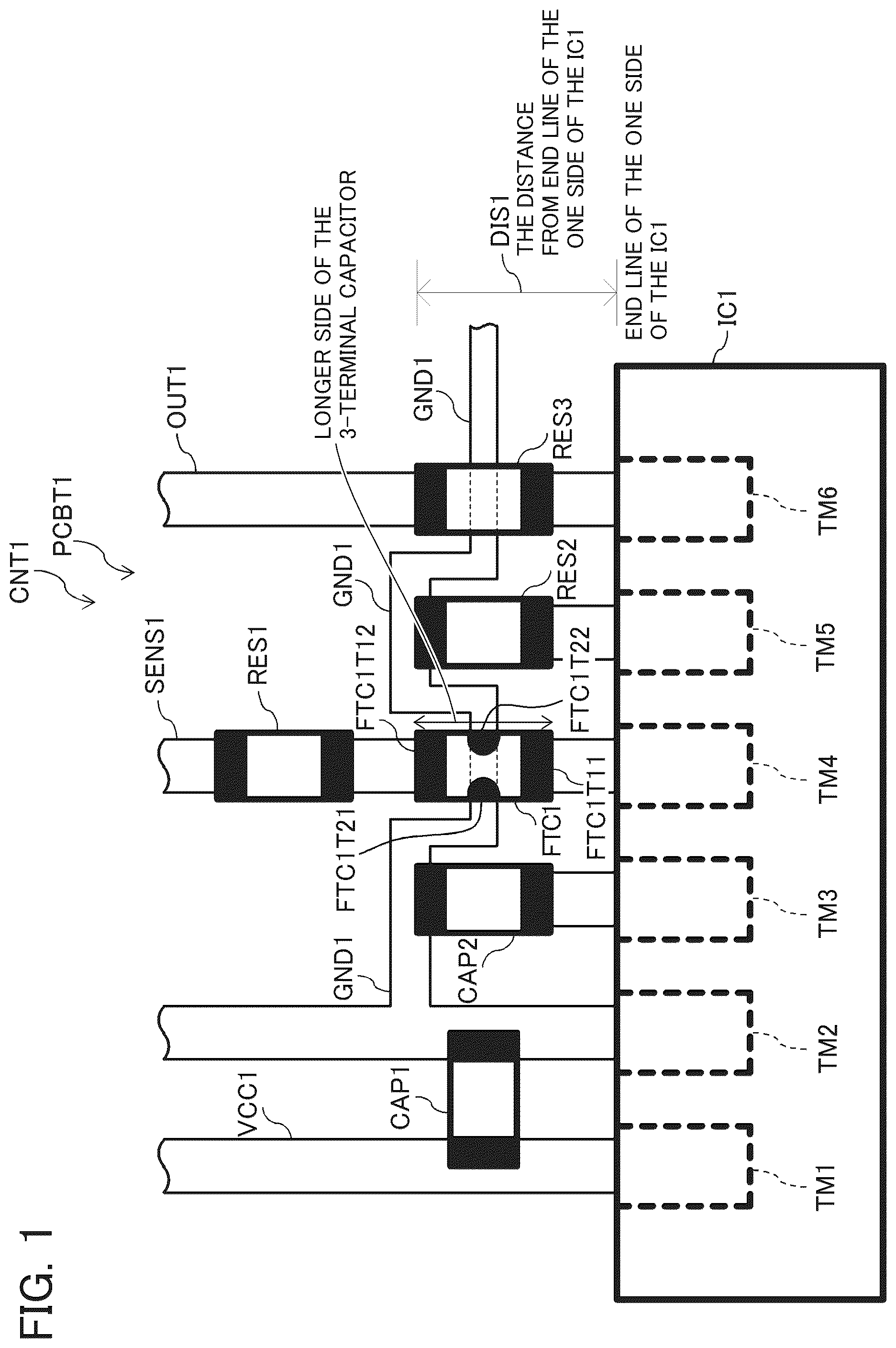
illustrates the control circuit CNT 1 formed on a PCB (PCB's surface PCBT 1 ). An integrated circuit (IC) IC 1 includes six terminals TM 1 to TM 6 . TM 1 is a 3.3V power supply terminal, TM 2 is a GND terminal, TM 3 is an inner power supply terminal, TM 4 is a sensing terminal, TM 5 is a control terminal, and TM 6 is a signal output terminal. TM 1 to TM 6 are arranged on one side of IC 1 . In detail, they are disposed so as to be flush with the one side of IC 1 . TM 1 to TM 6 are denoted by dotted lines in order to indicate that they are located under IC 1 .
A power supply wire VCC 1 is connected to TM 1 . A GND wire GND 1 is connected to TM 2 . VCC 1 and GND 1 are conductive wire patterns (traces) formed on the PCB. GND 1 is wired in a direction along the one side of the IC 1 . The power supply wire can be replaced with GND 1 , and the GND wire can be replaced with VCC 1 , in accordance with the specifications of the IC 1 's terminals.
An input capacitor CAP 1 is connected to TM 1 and TM 2 via VCC 1 and GND 1 . An inner power supply capacitor CAP 2 has one end connected to TM 3 , and the other end connected to GND 1 .
The one end of CAP 2 , although being connected to TM 3 via a wire, may be directly connected to TM 3 . This “connection via a wire” or “direct connection”, which is irrelevant to the circuit configuration, is described merely as “connection”. The connections to TM 4 to TM 6 , and the connection between a first resistor RES 1 and FTC 1 T 12 are likewise described as “connection”.
A sense signal line SENS 1 is connected to TM 4 via RES 1 and the FTC 1 's feedthrough electrode (FTC 1 T 11 and FTC 1 T 12 ) connected in series.
FTC 1 T 21 and FTC 1 T 22 are connected to GND 1 . FTC 1 in and FTC 1 in are the same element.
GND 1 , which passes under FTC 1 , is denoted by a dotted line in the drawing. GND 1 in this dotted-line portion, even having no wiring, is still the same in terms of a circuit. This is because that FTC 1 T 21 and FTC 1 T 22 are connected together inside FTC 1 . CNT 1 can include FTC 2 in place of FTC 1 .
A second resistor RES 2 has one end connected to TM 5 , and the other end connected to GND 1 .
A third resistor RES 3 has one end connected to TM 6 , and the other end connected to a signal line OUT 1 .
RES 3 straddles GND 1 , and thus, GND 1 under RES 3 is denoted by a dotted line in the drawing. RES 3 , which straddles, is not connected to anything except TM 6 and the signal line OUT 1 .
CAP 1 , CAP 2 , RES 1 , RES 2 and RES 3 are surface-mount components each having one end and the other end. These resistors or capacitors can be changed as appropriate into a capacitor, a resistor, an inductance, a diode or other kinds in accordance with the specifications of CNT 1 or IC 1 . These components, which can be changed irrespective of kinds, are on the whole referred also to as a component in the present disclosure.
Further, this component, FTC 1 , IC 1 and the wires are all formed on the PCB's front surface. All can be formed on the back surface as well, as necessary.
Main Configuration of Control Circuit
CNT 1 is formed on the PCB.
CNT 1 includes IC 1 , FTC 1 , and RES 2 or RES 3 , both of which are first components.
IC 1 has a structure where four or more terminals are arranged on one side of IC 1 .
FTC 1 includes a feedthrough electrode and a reference electrode.
The first component has one end and the other end.
FTC 1 and the first component are surface-mount components.
The PCB includes GND 1 , which is a first wire.
The first wire is wired in a direction along the one side of the IC.
The first wire needs to avoid any component terminal on the PCB, and to connect a terminal of any component. To achieve both of this avoidance and connection, the first wire, although being wired in a curved line rather than in a straight line, is wired in the direction along the one side of IC 1 as a whole. The first wire is wired on the same plane as the plane where FTC 1 and the first component are mounted. That the first wire is wired in the direction along the one side of IC 1 can be referred also to as that the first wire is substantially parallel with the one side of IC 1 as a whole. The word “substantially parallel” means an angle of, for instance, 0 to 45 degrees; for instance, an angle of more than 45 degrees complicates the wire layout.
FTC 1 is configured such that one end of the feedthrough electrode is connected to any terminal of IC 1 , and such that the reference electrode is connected to the first wire.
The one end of the first component is connected to any terminal of IC 1 , and the first component “straddles the first wire” or “connects the first wire to the other end”.
CNT 1 like this enables FTC 1 and/or the first component to be connected to the first wire wired in the direction along the one side of IC 1 . This can simplify the wire layout.
Additional Configuration of Control Circuit
The first wire is a power supply or a GND connected to IC 1 . CNT 1 is formed on either the front surface or back surface of the PCB.
Using the first wire can stabilize the IC 1 's circuit control when this wire is a stable potential, such as a power supply or a GND.
The circuit constituting CNT 1 is formed on either the front surface or back surface of the PCB, thus facilitating simplification of the wire layout.
FTC 1 and the first component are disposed in a range from the one side of IC 1 to 10 times of the length of the longer side of FTC 1 .
The FTC 1 's longer side measures 1 mm for instance. FTC 1 and “RES 2 or RES 3 ” are disposed within, for instance, 1.6 mm of an arrow DIS 1 from the one side of IC 1 . FTC 1 and “RES 2 or RES 3 ” are disposed in a range of 10 times of the length of the FTC 1 's longer side, thus facilitating simplification of the wire layout.
CNT 1 further includes a second component. The second component has one end and the other end.
The one end of the second component is connected to any terminal of IC 1 . The second component straddles the first wire. The first component connects the first wire to the other end.
To be specific, the second component is RES 3 and staddles GND 1 , and its one end is connected to IC 1 . The first component is RES 2 , its one end is connected to IC 1 , and its other end is connected to GND 1 .
Second Preferred Embodiment
illustrates an instance where CNT 1 is connected to a power supply circuit.
An auxiliary power supply circuit PW 1 is connected for supplying electric power to CNT 1 . CNT 1 is connected for controlling a main power supply circuit PW 2 . A power supply device PUI includes CNT 1 , PW 1 , and PW 2 .
PUI can be equipped with CNT 1 having a simplified layout.
It should be noted that each of the foregoing numeric values is a mere example. To adjust circuit operations, a resistor can be inserted into a wire as appropriate, or a capacitor can be added between wires as appropriate.
Additional Note
One aspect of the present disclosure is not limited to the foregoing preferred embodiments. Various modifications can be devised within the scope of the claims. A preferred embodiment that is obtained in combination, as appropriate, with the technical means disclosed in the respective preferred embodiments is also included in the technical scope of one aspect of the present disclosure. Furthermore, combining the technical means disclosed in the respective preferred embodiments can form a new technical feature.
Figures (2)
Citations
This patent cites (36)
- US4584627
- US5379189
- US5844762
- US6473291
- US6936914
- US6995629
- US7881040
- US7929315
- US9468994
- US9538634
- US9743522
- US9844135
- US9998084
- US10178770
- US10250215
- US10361631
- US10470296
- US10477676
- US10606792
- US10764991
- US10770206
- US10892316
- US11202914
- US11744020
- US2004/0119553
- US2006/0022320
- US2007/0123949
- US2007/0253177
- US2012/0229998
- US2017/0323729
- US2018/0317317
- US2021/0111626
- US2024/0314924
- US2025/0016911
- US2020039625
- US2016092833