Abstract
A multilayer varistor includes a sintered body and a first internal electrode, a second internal electrode, a third internal electrode, and a fourth internal electrode which are disposed in the sintered body. The first internal electrode, the second internal electrode, the third internal electrode, and the fourth internal electrode are arranged in an order of the first internal electrode, the third internal electrode, the fourth internal electrode, and the second internal electrode from a side of a first main face. The third internal electrode and the fourth internal electrode are electrically connected to each other. At least part of the first internal electrode and at least part of the third internal electrode overlap each other when viewed in a third direction. At least part of the second internal electrode and at least part of the fourth internal electrode overlap each other when viewed in the third direction.
Claims (20)
1. A multilayer varistor comprising: a sintered body having a first end face and a second end face opposite to each other in a first direction, a first side face and a second side face opposite to each other in a second direction intersecting the first direction, and a first main face and a second main face opposite to each other in a third direction intersecting the first direction and the second direction; a first internal electrode; a second internal electrode; a third internal electrode; and a fourth internal electrode, wherein: the first internal electrode, the second internal electrode, the third internal electrode, and the fourth internal electrode are disposed in the sintered body, the first internal electrode, the second internal electrode, the third internal electrode, and the fourth internal electrode are arranged in an order of the first internal electrode, the third internal electrode, the fourth internal electrode, and the second internal electrode from a side of the first main face, the third internal electrode and the fourth internal electrode are electrically connected to each other, at least part of the first internal electrode and at least part of the third internal electrode overlap each other when viewed in the third direction, at least part of the second internal electrode and at least part of the fourth internal electrode overlap each other when viewed in the third direction, the first internal electrode includes a first facing part and a first lead-out part which has a narrower width in the second direction than the first facing part, the third internal electrode includes a third facing part and a third lead-out part which has a narrower width in the first direction than the third facing part, and the third facing part is larger than the first facing part when viewed in the third direction.
Show 19 dependent claims
2. The multilayer varistor of claim 1 , wherein at least part of the third internal electrode and at least part of the fourth internal electrode overlap each other when viewed in the third direction.
3. The multilayer varistor of claim 1 , wherein at least part of the first internal electrode, at least part of the second internal electrode, at least part of the third internal electrode, and at least part of the fourth internal electrode overlap each other when viewed in the third direction.
4. The multilayer varistor of claim 1 , wherein a first distance between the third internal electrode and the fourth internal electrode along the third direction is longer than each of a second distance between the first internal electrode and the third internal electrode along the third direction and a third distance between the second internal electrode and the fourth internal electrode along the third direction.
5. The multilayer varistor of claim 2 , wherein a first distance between the third internal electrode and the fourth internal electrode along the third direction is longer than each of a second distance between the first internal electrode and the third internal electrode along the third direction and a third distance between the second internal electrode and the fourth internal electrode along the third direction.
6. The multilayer varistor of claim 3 , wherein a first distance between the third internal electrode and the fourth internal electrode along the third direction is longer than each of a second distance between the first internal electrode and the third internal electrode along the third direction and a third distance between the second internal electrode and the fourth internal electrode along the third direction.
7. The multilayer varistor of claim 1 , wherein a first distance between the third internal electrode and the fourth internal electrode along the third direction is 0.5 or more times each of a second distance between the first internal electrode and the third internal electrode along the third direction and a third distance between the second internal electrode and the fourth internal electrode along the third direction.
8. The multilayer varistor of claim 2 , wherein a first distance between the third internal electrode and the fourth internal electrode along the third direction is 0.5 or more times each of a second distance between the first internal electrode and the third internal electrode along the third direction and a third distance between the second internal electrode and the fourth internal electrode along the third direction.
9. The multilayer varistor of claim 3 , wherein a first distance between the third internal electrode and the fourth internal electrode along the third direction is 0.5 or more times each of a second distance between the first internal electrode and the third internal electrode along the third direction and a third distance between the second internal electrode and the fourth internal electrode along the third direction.
10. The multilayer varistor of claim 1 , wherein a first distance between the third internal electrode and the fourth internal electrode along the third direction is 1.2 or more times each of a second distance between the first internal electrode and the third internal electrode along the third direction and a third distance between the second internal electrode and the fourth internal electrode along the third direction.
11. The multilayer varistor of claim 2 , wherein a first distance between the third internal electrode and the fourth internal electrode along the third direction is 1.2 or more times each of a second distance between the first internal electrode and the third internal electrode along the third direction and a third distance between the second internal electrode and the fourth internal electrode along the third direction.
12. The multilayer varistor of claim 3 , wherein a first distance between the third internal electrode and the fourth internal electrode along the third direction is 1.2 or more times each of a second distance between the first internal electrode and the third internal electrode along the third direction and a third distance between the second internal elect rode and the fourth internal electrode along the third direction.
13. The multilayer varistor of claim 1 , wherein a fourth distance between the first main face and the first internal electrode along the third direction is longer than a second distance between the first internal electrode and the third internal electrode along the third direction, and a fifth distance between the second main face and the second internal electrode along the third direction is longer than a third distance between the second internal electrode and the fourth internal electrode along the third direction.
14. The multilayer varistor of claim 2 , wherein a fourth distance between the first main face and the first internal electrode along the third direction is longer than a second distance between the first internal electrode and the third internal electrode along the third direction, and a fifth distance between the second main face and the second internal electrode along the third direction is longer than a third distance between the second internal electrode and the fourth internal electrode along the third direction.
15. The multilayer varistor of claim 3 , wherein a fourth distance between the first main face and the first internal electrode along the third direction is longer than a second distance between the first internal electrode and the third internal electrode along the third direction, and a fifth distance between the second main face and the second internal electrode along the third direction is longer than a third distance between the second internal electrode and the fourth internal electrode along the third direction.
16. The multilayer varistor of claim 4 , wherein a fourth distance between the first main face and the first internal electrode along the third direction is longer than a second distance between the first internal electrode and the third internal electrode along the third direction, and a fifth distance between the second main face and the second internal electrode along the third direction is longer than a third distance between the second internal electrode and the fourth internal electrode along the third direction.
17. The multilayer varistor of claim 5 , wherein a fourth distance between the first main face and the first internal electrode along the third direction is longer than a second distance between the first internal electrode and the third internal electrode along the third direction, and a fifth distance between the second main face and the second internal electrode along the third direction is longer than a third distance between the second internal electrode and the fourth internal electrode along the third direction.
18. The multilayer varistor of claim 1 , further comprising: a fifth internal electrode between the first internal electrode and the first main face; and a sixth internal electrode between the second internal electrode and the second main face, wherein the fifth internal electrode is electrically connected to the third internal electrode, and the sixth internal electrode is electrically connected to the fourth internal electrode.
19. The multilayer varistor of claim 1 , further comprising: a first external electrode, a second external electrode, and a third external electrode which are disposed on a surface of the sintered body, wherein the first internal electrode is electrically connected to the first external electrode, the second internal electrode is electrically connected to the second external electrode, and the third internal electrode and the fourth internal electrode are electrically connected to the third external electrode.
20. The multilayer varistor of claim 1 , wherein a first capacitance between the first internal electrode and the third internal electrode and a second capacitance between the second internal electrode and the fourth internal electrode are each equal to or less than 200 pF, and a difference between the first capacitance and the second capacitance is less than or equal to 20% of the first capacitance.
Full Description
Show full text →
CROSS-REFERENCE TO RELATED APPLICATION
The present application is based upon and claims the benefit of priority to Japanese Patent Application No. 2022-045844 filed on Mar. 22, 2022, the entire contents of which are incorporated herein by reference.
TECHNICAL FIELD
The present disclosure relates to multilayer varistors, and particularly, to a multilayer varistor including a plurality of internal electrodes.
BACKGROUND ART
As household appliances and in-vehicle electronic devices are recently downsized, which also requires downsizing of varistors which are components of the household appliances and in-vehicle electronic devices. In addition, when the frequency of a circuit in which a varistor is used is increased, the capacitance of the varistor may make an effect on the performance (surge-absorbing performance by the varistor). Therefore, there is a demand for a varistor that has a small capacitance and a small variation in the capacitance while a predetermined varistor voltage is secured. When varistors are used in a pair, two varistors formed in one element are proposed in order to reduce differences in capacitance between the varistors in the pair. Note that Literature 1 (JP H07-235406 A) is known as an example of information on prior art documents relating to the invention of the present application.
A conventional multilayer varistor has the problem that a stray capacitance generated between an internal electrode constituting one varistor and an internal electrode constituting the other varistor tends to cause cross-talk in which a signal leaks from one internal terminal to the other internal terminal.
SUMMARY
In view of the foregoing, it is an object of the present disclosure to provide a multilayer varistor capable of suppressing the occurrence of cross-talk.
A multilayer varistor according to an aspect of the present disclosure includes a sintered body, and a first internal electrode, a second internal electrode, a third internal electrode, and a fourth internal electrode which are disposed in the sintered body. The sintered body includes a first end face and a second end face opposite to each other in a first direction, a first side face and a second side face opposite to each other in a second direction intersecting the first direction, and a first main face and a second main face opposite to each other in a third direction intersecting the first direction and the second direction. The first internal electrode, the second internal electrode, the third internal electrode, and the fourth internal electrode are arranged in an order of the first internal electrode, the third internal electrode, the fourth internal electrode, and the second internal electrode from a side of the first main face. The third internal electrode and the fourth internal electrode are electrically connected to each other. At least part of the first internal electrode and at least part of the third internal electrode overlap each other when viewed in the third direction. At least part of the second internal electrode and at least part of the fourth internal electrode overlap each other when viewed in the third direction.
BRIEF DESCRIPTION OF THE DRAWINGS
The figures depict one or more implementation in accordance with the present teaching, by way of example only, not by way of limitations. In the figures, like reference numerals refer to the same or similar elements.
is a transparent perspective view of a multilayer varistor according to an embodiment of the present disclosure;
is a sectional view of the multilayer varistor;
is a transparent top view of the multilayer varistor;
is a transparent bottom view of the multilayer varistor;
is a transparent top view of a multilayer varistor of a first variation;
is a transparent bottom view of the multilayer varistor of the first variation;
is a transparent top view of a multilayer varistor of a second variation;
is a sectional view of a multilayer varistor of a third variation;
is a sectional view of a multilayer varistor of a fourth variation;
is a sectional view of a multilayer varistor of a fifth variation;
is a transparent top view of the multilayer varistor of the fifth variation; and
is a transparent bottom view of the multilayer varistor of the fifth variation.
DETAILED DESCRIPTION
A multilayer varistor 1 according to an embodiment of the present disclosure will be described in detail with reference to the drawings. Note that the embodiment and variations described below are merely examples of the present disclosure, and the present disclosure is not limited to the embodiment and the variations. The present disclosure may be modified variously without departing from the scope of technical idea of the present disclosure, even if not including the embodiment and the variations, according to design or the like. Further, the embodiment described below (including the variations) may be implemented by appropriately in combination.
(1) Overview
The overview of the multilayer varistor 1 will be described below with reference to to 4 . Figures described in the following embodiment are schematic views, and the ratio of sizes and the ratio of thicknesses of components in the figures do not necessarily reflect actual dimensional ratios.
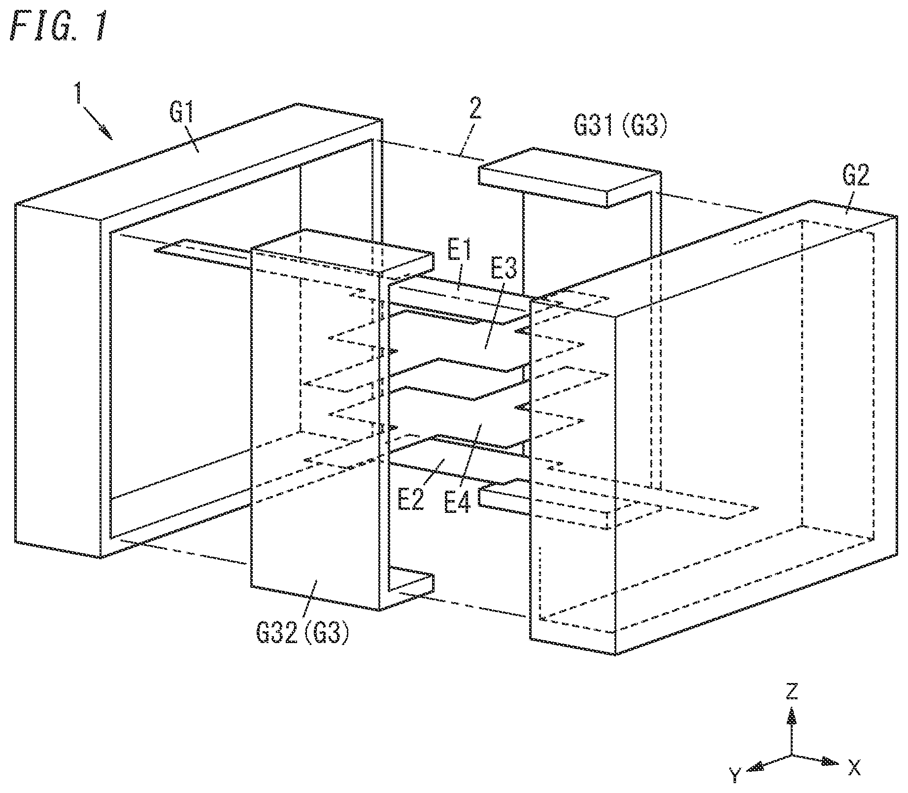
The multilayer varistor 1 includes a sintered body 2 , and a first internal electrode E 1 , a second internal electrode E 2 , a third internal electrode E 3 , and a fourth internal electrode E 4 which are disposed in the sintered body 2 .
The sintered body 2 includes a first end face S 11 and a second end face S 12 opposite to each other in a first direction, a first side face S 21 and a second side face S 22 opposite to each other in a second direction intersecting the first direction, and a first main face S 31 and a second main face S 32 opposite to each other in a third direction intersecting the first direction and the second direction.
The first internal electrode E 1 , the second internal electrode E 2 , the third internal electrode E 3 , and the fourth internal electrode E 4 are arranged in the order of the first internal electrode E 1 , the third internal electrode E 3 , the fourth internal electrode E 4 , and the second internal electrode E 2 from the side of the first main face S 31 .
The third internal electrode E 3 and the fourth internal electrode E 4 are electrically connected to each other.
When viewed in the third direction, at least part of the first internal electrode E 1 and at least part of the third internal electrode E 3 overlap each other.
When viewed in the third direction, at least part of the second internal electrode E 2 and at least part of the fourth internal electrode E 4 overlap each other.
In the multilayer varistor 1 of the present embodiment, a first varistor region A 1 is formed between the first internal electrode E 1 and the third internal electrode E 3 , and a second varistor area A 2 is formed between the second internal electrode E 2 and the fourth internal electrode E 4 . In the first varistor region A 1 , a surge current flows when a surge voltage is applied between the first internal electrode E 1 and the third internal electrode E 3 . In the second varistor area A 2 , a surge current flows when a surge voltage is applied between the second internal electrode E 2 and the fourth internal electrode E 4 .
The multilayer varistor 1 is used by being arranged in the vicinity of a communication IC configured to perform communication based on, for example, a two-wire differential voltage transmission scheme. To the communication IC, lands of two signal lines and a land of a ground line are connected. Here, the first internal electrode E 1 and the second internal electrode E 2 are electrically connected to the lands of the two signal lines on a one-to-one basis. The third internal electrode E 3 and the fourth internal electrode E 4 are electrically connected to the land of the ground line.
According to the embodiment described above, a distance is provided between the third internal electrode E 3 and the fourth internal electrode E 4 , and therefore, the distance between the first internal electrode E 1 and the second internal electrode E 2 can be greater than that in the case where functions of the third internal electrode E 3 and the fourth internal electrode E 4 are implemented by a single internal electrode. This can reduce the stray capacitance between the first internal electrode E 1 and the second internal electrode E 2 and thus can suppress the occurrence of cross-talk in which a signal leaks from the first internal electrode E 1 constituting the first varistor region A 1 to the second internal electrode E 2 constituting the second varistor area A 2 .
(2) Details
The multilayer varistor 1 of the present embodiment will be described in detail below with reference to to 4 .
is a transparent perspective view of the multilayer varistor 1 , is a sectional view of the multilayer varistor 1 , is a transparent top view of the multilayer varistor 1 , and is a transparent bottom view of the multilayer varistor 1 .
As described above, the multilayer varistor 1 includes the sintered body 2 and, for example, four internal electrodes (the first internal electrode E 1 , the second internal electrode E 2 , the third internal electrode E 3 , and the fourth internal electrode E 4 ) which are disposed in the sintered body 2 . The number of internal electrodes is not limited to four but may be changed as appropriate. The multilayer varistor 1 further includes a first external electrode G 1 , a second external electrode G 2 , and a third external electrode G 3 disposed on a surface of the sintered body 2 . The first internal electrode E 1 is electrically connected to the first external electrode G 1 . The second internal electrode E 2 is electrically connected to the second external electrode G 2 . The third internal electrode E 3 and the fourth internal electrode E 4 are electrically connected to the third external electrode G 3 . That is, the third internal electrode E 3 and the fourth internal electrode E 4 are electrically connected to each other via the third external electrode G 3 .
The sintered body 2 is, for example, in the shape of a rectangular parallelepiped having a length of 1.6 mm, a width of 0.8 mm, and a height of 0.8 mm. In and other figures, the outer shape of the sintered body 2 is shown in the shape of a rectangular parallelepiped, but corner portions of the sintered body 2 may be appropriately beveled, or the corner portions of the sintered body 2 may be rounded.
In the following description, the long side direction (left/right direction) of the sintered body 2 is defined as an “X-axis direction”, the depth direction (forward/backward direction) of the sintered body 2 is defined as a “Y-axis direction”, and the thickness direction (up/down direction) of the sintered body 2 is defined as a “Z-axis direction”. The X axis, the Y axis, and the Z axis defining these directions are orthogonal to each other. Moreover, the positive direction of the X axis is defined as a right side, the positive direction of the Y axis is defined as a forward side, and the positive direction of the Z axis is defined as an upside. However, these directions are only examples and should not be construed as limiting the directions of the multilayer varistor 1 in use. In addition, the arrows indicating the “X-axis direction”, the “Y-axis direction”, and the “Z-axis direction” on the drawings are shown only for the purpose of explanation and are intangible.
The sintered body 2 has, as shown in to 4 , the first end face S 11 and the second end face S 12 opposite to each other in the X-axis direction, the first side face S 21 and the second side face S 22 opposite to each other in the Y-axis direction, and the first main face S 31 and the second main face S 32 opposite to each other in the Z-axis direction. That is, the X-axis direction corresponds to the “first direction” in which the first end face S 11 and the second end face S 12 are opposite to each other. The Y-axis direction corresponds to the “second direction” in which the first side face S 21 and the second side face S 22 are opposite to each other. The Z-axis direction corresponds to the “third direction” in which the first main face S 31 and the second main face S 32 are opposite to each other.
The sintered body 2 includes a semiconductor ceramic component having a non-linearity resistance characteristic. The sintered body 2 , for example, includes ZnO as a major component, may include, as a minor component, at least one selected from the group consisting of Bi 2 O 3 , Co 2 O 3 , MnO 2 , and Sb 2 O 3 , and may include at least one selected from the group consisting of Pr 6 O 11 , Co 2 O 3 , CaCO 3 , and Cr 2 O 3 . In the sintered body 2 , ZnO is sintered, and the other minor components are deposited on the grain boundary of ZnO particles. A grain boundary barrier formed between the ZnO particles expresses the non-linearity resistance characteristic. The sintered body 2 is formed, for example, by stacking five layers LY 1 to LY 5 (see ) including ZnO as a major component on one another in the third direction and then sintering the five layers LY 1 to LY 5 . The surface of the sintered body 2 may be covered with a high-resistance layer having a higher resistance than the sintered body 2 .
The first external electrode G 1 , the second external electrode G 2 , and the third external electrode G 3 are disposed on the surface of the sintered body 2 . As shown in , the multilayer varistor 1 of the present embodiment includes two third external electrodes G 3 (third external electrodes G 31 , G 32 ). That is, the multilayer varistor 1 of the present embodiment is a so-called four-terminal multilayer varistor. The number of the third external electrodes G 3 is not limited to two but may be one or three or more.
The first external electrode G 1 , the second external electrode G 2 , and the third external electrodes G 31 and G 32 are made of, for example, metal such as silver, copper, platinum, or an alloy thereof. The first external electrode G 1 , the second external electrode G 2 , and the third external electrodes G 31 and G 32 may include a primary electrode made of metal such as silver, copper, platinum, or an alloy thereof and a secondary electrode made of a plated layer of nickel, tin, or the like formed on a surface of the primary electrode.
The first external electrode G 1 and the second external electrode G 2 are formed, for example, by dipping each of the first end face S 11 and the second end face S 12 of the sintered body 2 into a conductive paste.
The first external electrode G 1 is disposed on the entire surface of the first end face S 11 and on a left end portion of each of the first side face S 21 , the second side face S 22 , the first main face S 31 , and the second main face S 32 .
The second external electrode G 2 is disposed on the entire surface of the second end face S 12 and on a right end portion of each of the first side face S 21 , the second side face S 22 , the first main face S 31 , and the second main face S 32 .
The third external electrodes G 31 and G 32 are formed by, for example, roller-transferring of a conductive paste onto the surface of the sintered body 2 .
The third external electrode G 31 is disposed on a central portion of the first side face S 21 , the center of a rear end portion of the first main face S 31 , and the center of a rear end portion of the second main face S 32 .
The third external electrode G 32 is disposed on a central portion of the second side face S 22 , the center of a front end portion of the first main face S 31 , and the center of a front end portion of the second main face S 32 .
The first internal electrode E 1 , the second internal electrode E 2 , the third internal electrode E 3 , and the fourth internal electrode E 4 are disposed in the sintered body 2 .
Here, as described above, the sintered body 2 includes the five layers LY 1 to LY 5 (see ) stacked on one another in the third direction. As shown in , the layers LY 1 to LY 5 are stacked in the order of the layers LY 1 , LY 2 , LY 3 , LY 4 , and LY 5 from the top.
The first internal electrode E 1 is disposed, for example, on an upper surface of the layer LY 2 (hereinafter also referred to as a first laminated surface SF 1 ). The second internal electrode E 2 is disposed, for example, on an upper surface of the layer LY 5 (hereinafter also referred to as a second aminated surface SF 2 ). The third internal electrode E 3 is disposed, for example, on an upper surface of the layer LY 3 (hereinafter referred to as a third laminated surface SF 3 ). The fourth internal electrode E 4 is disposed, for example, on an upper surface of the layer LY 4 (hereinafter also referred to as a fourth laminated surface SF 4 ). Thus, in the third direction (up/down direction), the first internal electrode E 1 , the second internal electrode E 2 , the third internal electrode E 3 , and the fourth internal electrode E 4 are arranged such that the first internal electrode E 1 , the third internal electrode E 3 , the fourth internal electrode E 4 , and the second internal electrode E 2 are separated from each other in this order from the side of the first main face S 31 . Specifically, as shown in , the third internal electrode E 3 and the fourth internal electrode E 4 are spaced apart from each other by a first distance D 1 along the third direction. The first internal electrode E 1 and the third internal electrode E 3 are spaced apart from each other by a second distance D 2 along the third direction. The second internal electrode E 2 and the fourth internal electrode E 4 are spaced apart from each other by a third distance D 3 along the third direction.
Here, the first distance D 1 is preferably 0.5 or more times each of the second distance D 2 and the third distance D 3 . In the present embodiment, the first distance D 1 is a distance longer than each of the second distance D 2 and the third distance D 3 . More preferably, the first distance D 1 is 1.2 or more times each of the second distance D 2 and the third distance D 3 .
Accordingly, the distance between the first internal electrode E 1 and the second internal electrode E 2 is longer than each of the second distance D 2 and the third distance D 3 , which can reduce the stray capacitance between the first internal electrode E 1 and the second internal electrode E 2 , thereby suppressing the occurrence of cross-talk.
The first internal electrode E 1 is spaced apart from the first main face S 31 by a fourth distance D 4 along the third direction. The fourth distance D 4 is a distance longer than the second distance D 2 .
Accordingly, the distance between the first internal electrode E 1 and the part of the second external electrode G 2 provided on the right end portion of the first main face S 31 is satisfactorily longer than the second distance D 2 . Here, as described above, the second external electrode G 2 is electrically connected to the second internal electrode E 2 . Therefore, the stray capacitance between the first internal electrode E 1 and the second internal electrode E 2 can be reduced, thereby suppressing the occurrence of cross-talk.
The second internal electrode E 2 is spaced apart from the second main face S 32 by a fifth distance D 5 along the third direction. The fifth distance D 5 is a distance longer than the third distance D 3 .
Accordingly, the distance between the second internal electrode E 2 and the part of the first external electrode G 1 provided on the left end portion of the second main face S 32 is satisfactorily longer than the third distance D 3 . Here, as described above, the first external electrode G 1 is electrically connected to the first internal electrode E 1 . Therefore, the stray capacitance between the first internal electrode E 1 and the second internal electrode E 2 can be reduced, thereby suppressing the occurrence of cross-talk.
As shown in , the first internal electrode E 1 includes a first facing part F 1 and a first lead-out part B 1 . The first lead-out part B 1 has a narrower width in the second direction than the first facing part F 1 and protrudes leftward from the first facing part F 1 along the first direction. The first lead-out part B 1 has a left end electrically connected to the first external electrode G 1 .
The second internal electrode E 2 has a second facing part F 2 and a second lead-out part B 2 . The second lead-out part B 2 has a narrower width in the second direction than the second facing part F 2 and protrudes rightward from the second facing part F 2 along the first direction. The second lead-out part B 2 has a right end electrically connected to the second external electrode G 2 .
The width of the first facing part F 1 in the second direction is equal to the width of the second facing part F 2 in the second direction, for example. Further, the width of the first facing part F 1 in the first direction is equal to the width of the second facing part F 2 in the first direction, for example.
The third internal electrode E 3 has a third facing part F 3 and, for example, two third lead-out parts B 3 . Each of the two third lead-out parts B 3 has a narrower width in the first direction than the third facing part F 3 , one of the third lead-out parts B 3 protrudes forward from the third facing part F 3 along the second direction, and the other of the third lead-out parts B 3 protrudes backward from the third facing part F 3 along the second direction. The third lead-out part B 3 protruding backward is electrically connected to the third external electrode G 31 , and the third lead-out part B 3 protruding forward is electrically connected to the third external electrode G 32 .
The fourth internal electrode E 4 has a fourth facing part F 4 and two fourth lead-out parts B 4 . The two fourth lead-out parts B 4 each have a narrower width in the first direction than the fourth facing part F 4 , one of the fourth lead-out parts B 4 protrudes forward from the fourth facing part F 4 along the second direction, and the other of the fourth lead-out parts B 4 protrudes backward from the fourth facing part F 4 along the second direction. The fourth lead-out part B 4 protruding backward is electrically connected to the third external electrode G 31 , and the fourth lead-out part B 4 protruding frontward is electrically connected to the third external electrode G 32 . Therefore, the third internal electrode E 3 and the fourth internal electrode E 4 are electrically connected to each other via the third external electrodes G 31 and G 32 .
As shown in , the first internal electrode E 1 and the third internal electrode E 3 are arranged such that at least part of the first internal electrode E 1 and at least part of the third internal electrode E 3 overlap each other when viewed from above. Specifically, when viewed from above, the third facing part F 3 of the third internal electrode E 3 is larger than the first facing part F 1 of the first internal electrode E 1 , and thus, the first facing part F 1 and part of the first lead-out part B 1 are included in the third facing part F 3 . Thus, the first varistor region A 1 is formed between the third facing part F 3 and a set of the first facing part F 1 and the part of the first lead-out part B 1 . The first varistor region A 1 preferably has a first capacitance of less than or equal to 200 pF.
Further, as shown in , the second internal electrode E 2 and the fourth internal electrode E 4 are arranged such that at least part of the second internal electrode E 2 and at least part of the fourth internal electrode E 4 overlap each other when viewed from below. Specifically, when viewed from below, the fourth facing part F 4 of the fourth internal electrode E 4 is larger than the second facing part F 2 of the second internal electrode E 2 , and thus, the second facing part F 2 and part of the second lead-out part B 2 are included in the fourth facing part F 4 . Thus, the second varistor area A 2 is formed between the fourth facing part F 4 and a set of the second facing part F 2 and the part of the second lead-out part B 2 . The second varistor area A 2 preferably has a second capacitance of less than or equal to 200 pF. The difference between the first capacitance and the second capacitance is preferably less than or equal to 20% of the first capacitance. This can reduce the effect of the difference between the first capacitance and the second capacitance on the surge-absorbing property of the multilayer varistor 1 .
Further, the third internal electrode E 3 and the fourth internal electrode E 4 are arranged such that at least part of the third internal electrode E 3 and at least part of the fourth internal electrode E 4 overlap each other when viewed in the third direction. Specifically, the third internal electrode E 3 and the fourth internal electrode E 4 are formed to have the same shape when viewed in the third direction, and the third internal electrode E 3 and the fourth internal electrode E 4 overlap each other in the entire area thereof when viewed in the third direction, for example.
Therefore, in the present embodiment, the first internal electrode E 1 , the second internal electrode E 2 , the third internal electrode E 3 , and the fourth internal electrode E 4 are arranged such that at least part of the first internal electrode E 1 , at least part of the second internal electrode E 2 , at least part of the third internal electrode E 3 , and at least part of the fourth internal electrode E 4 overlap each other when viewed in the third direction.
Accordingly, the at least part of the third internal electrode E 3 and the at least part of the fourth internal electrode E 4 shield the at least part of the first internal electrode E 1 from the at least part of the second internal electrode E 2 , and the occurrence of cross-talk can thus be suppressed. In addition, this makes the multilayer varistor 1 downsized.
(3) Variations
Variations of the embodiment will be described below. However, the same reference numerals are given to the same constituent elements as those in the embodiment, and description thereof will be omitted as appropriate. Further, the configurations of the variations described below can be appropriately combined with the configuration described in the embodiment.
(3.1) First Variation
As shown in , a multilayer varistor 1 A of a first variation includes a first internal electrode E 1 and a second internal electrode E 2 which are arranged so as not to overlap each other when viewed in the third direction. Specifically, in the multilayer varistor 1 A, the first internal electrode E 1 and the second internal electrode E 2 are aligned in the forward/backward direction when viewed in the third direction.
In the multilayer varistor 1 A, for example, a third facing part F 3 of a third internal electrode E 3 and a fourth facing part F 4 of a fourth internal electrode E 4 are arranged side by side in the forward/backward direction when viewed in the third direction. In other words, the third facing part F 3 of the third internal electrode E 3 and the fourth facing part F 4 of the fourth internal electrode E 4 are disposed at locations where they do not overlap each other when viewed in the third direction. In this variation, the third facing part F 3 is larger than a first facing part F 1 , and thus, the first facing part F 1 and part of a first lead-out part B 1 are included in the third facing part F 3 as in the embodiment described above. Further, when viewed from below, the fourth facing part F 4 is larger than a second facing part F 2 , and thus, the second facing part F 2 and part of a second lead-out part B 2 are included in the fourth facing part F 4 as in the embodiment described above.
Accordingly, the distance between the first internal electrode E 1 and the second internal electrode E 2 can be made greater than that in the embodiment described above, and therefore, the stray capacitance between the first internal electrode E 1 and the second internal electrode E 2 can be reduced, thereby suppressing the occurrence of cross-talk.
The first internal electrode E 1 and the second internal electrode E 2 may be arranged side by side in the left/right direction when viewed in the third direction.
(3.2) Second Variation
As shown in , a multilayer varistor 1 B of a second variation is configured such that the width of a first lead-out part B 1 in the second direction is equal to the width of a first facing part F 1 in the second direction. In addition, the width of a second lead-out part B 2 in the second direction is equal to the width of a second facing part F 2 in the second direction.
Thus, the connection stability of the first lead-out part B 1 with a first external electrode G 1 and the connection stability of the second lead-out part B 2 with a second external electrode G 2 can be improved.
(3.3) Third Variation
As shown in , a multilayer varistor 1 C of a third variation includes a first internal electrode E 1 , a second internal electrode E 2 , a third internal electrode E 3 , and a fourth internal electrode E 4 which are in a sintered body 2 . The multilayer varistor 1 C further includes a fifth internal electrode E 5 and a sixth internal electrode E 6 .
The fifth internal electrode E 5 is disposed between the first internal electrode E 1 and a first main face S 31 .
The fifth internal electrode E 5 is electrically connected to the third internal electrode E 3 . Specifically, the fifth internal electrode E 5 is electrically connected to a third external electrode G 3 . That is, the fifth internal electrode E 5 is electrically connected to the third internal electrode E 3 via the third external electrode G 3 .
The sixth internal electrode E 6 is disposed between the second internal electrode E 2 and a second main face S 32 .
The sixth internal electrode E 6 is electrically connected to the fourth internal electrode E 4 . Specifically, the sixth internal electrode E 6 is electrically connected to the third external electrode G 3 . In other words, the sixth internal electrode E 6 is electrically connected to the fourth internal electrode E 4 via the third external electrode G 3 .
The fifth internal electrode E 5 covers, for example, a first facing part F 1 of the first internal electrode E 1 . Thus, the fifth internal electrode E 5 can shield the first facing part F 1 from a second external electrode G 2 disposed at a right end of the first main face S 31 , thereby suppressing the occurrence of cross-talk. Further, a varistor region is formed also between the first facing part F 1 and the fifth internal electrode E 5 , thereby increasing the surge-current tolerance of the multilayer varistor 1 C.
The sixth internal electrode E 6 covers, for example, a second facing part F 2 of the second internal electrode E 2 . Thus, the sixth internal electrode E 6 can shield the second facing part F 2 from a first external electrode G 1 provided at a left end of the second main face S 32 , thereby suppressing the occurrence of cross-talk. Further, a varistor region is formed also between the second facing part F 2 and the sixth internal electrode E 6 , thereby increasing the surge-current tolerance of the multilayer varistor 1 C.
(3.4) Fourth Variation
As shown in , a multilayer varistor 1 D of a fourth variation includes, for example, two first internal electrodes E 1 (E 11 , E 12 ), for example, two second internal electrodes E 2 (E 21 , E 22 ), for example, three third internal electrodes E 3 (E 31 , E 32 , E 33 ), and for example, three fourth internal electrodes E 4 (E 41 , E 42 , E 43 ) which are in a sintered body 2 .
These internal electrodes are arranged in the order of the third internal electrode E 31 , the first internal electrode E 11 , the third internal electrode E 32 , the first internal electrode E 12 , the third internal electrode E 33 , the fourth internal electrode E 41 , the second internal electrode E 21 , the fourth internal electrode E 42 , the second internal electrode E 22 , and the fourth internal electrode E 43 from the side of a first main face S 31 .
The first internal electrodes E 11 and E 12 are electrically connected to a first external electrode G 1 .
The second internal electrodes E 21 and E 22 are electrically connected to a second external electrode G 2 .
The third internal electrodes E 31 , E 32 , and E 33 are electrically connected to a third external electrode G 3 .
The fourth internal electrode E 41 , E 42 , and E 43 are electrically connected to the third external electrode G 3 .
The third internal electrode E 31 covers, for example, a first facing part F 11 of the first internal electrode E 11 . Thus, the third internal electrode E 31 can shield the first facing part F 11 from the second external electrode G 2 provided at a right end of the first main face S 31 , thereby suppressing the occurrence of cross-talk. Further, a varistor region is formed also between the first facing part F 11 and the third internal electrode E 31 , thereby increasing the surge-current tolerance of the multilayer varistor 1 D.
The fourth internal electrode E 43 covers, for example, a second facing part F 22 of the second internal electrode E 22 . Thus, the fourth internal electrode E 43 can shield the second facing part F 22 from the first external electrode G 1 provided on a left end of a second main face S 32 , thereby suppressing the occurrence of cross-talk. Further, a varistor region is formed also between the second facing part F 22 and the fourth internal electrode E 43 , thereby increasing the surge-current tolerance of the multilayer varistor 1 D.
(3.5) Fifth Variation
As shown in to 12 , a multilayer varistor 1 E of a fifth variation is a so-called eight-terminal multilayer varistor.
The multilayer varistor 1 E includes a first external electrode G 1 E (G 11 E) and a second external electrode G 2 E (G 21 E) arranged side by side in the first direction on a central portion of a first side face S 21 . On the first side face S 21 , a third external electrode G 3 E (G 31 E) is disposed on the left side of the first external electrode G 11 E, and a third external electrode G 3 E (G 32 E) is disposed on the right side of the second external electrode G 21 E. That is, in the first direction, the third external electrode G 31 E, the first external electrode G 11 E, the second external electrode G 21 E, and the third external electrode G 32 E are arranged in this order.
Similarly, a first external electrode G 1 E (G 12 E) and a second external electrode G 2 E (G 22 E) are arranged side by side in the first direction on a central portion of a second side face S 22 . On the second side face S 22 , a third external electrode G 3 E (G 33 E) is disposed on the left side of the first external electrode G 12 E, and a third external electrode G 3 E(G 34 E) is disposed on the right side of the second external electrode G 22 E. That is, in the first direction, the third external electrode G 33 E, the first external electrode G 12 E, the second external electrode G 22 E, and the third external electrode G 34 E are arranged in this order.
As shown in , in the multilayer varistor 1 E, a first internal electrode E 1 E, a third internal electrode E 3 E, a fourth internal electrode E 4 E, and a second internal electrode E 2 E are arranged, in a sintered body 2 , in this order from the side of a first main face S 31 , wherein these electrodes are separated from each other. The third internal electrode E 3 E and the fourth internal electrode E 4 E are spaced apart from each other by a first distance DIE along the third direction. The first internal electrode E 1 E and the third internal electrode E 3 E are spaced apart from each other by a second distance D 2 E along the third direction. The second internal electrode E 2 E and the fourth internal electrode E 4 E are spaced apart from each other by a third distance D 3 E along the third direction. The first distance DIE is a distance longer than each of the second distance D 2 E and the third distance D 3 E.
The first internal electrode E 1 E is spaced apart from the first main face S 31 by a fourth distance D 4 E along the third direction. The fourth distance D 4 E is a distance longer than the second distance D 2 E.
The second internal electrode E 2 E is spaced apart from a second main face S 32 by a fifth distance D 5 E along the third direction. The fifth distance D 5 E is a distance longer than the third distance D 3 E.
The first internal electrode E 1 E includes a first facing part F 1 E and two first lead-out parts B 1 E. In the first direction, each first lead-out part B 1 E has a narrower width than the first facing part F 1 E. One of the two first lead-out parts B 1 E protrudes forward from the first facing part F 1 E, and the other of the two first lead-out parts B 1 E protrudes backward from the first facing part F 1 E. The first lead-out part B 1 E protruding backward is electrically connected to the first external electrode G 11 E, and the first lead-out part B 1 E protruding forward is electrically connected to the first external electrode G 12 E.
The second internal electrode E 2 E includes a second facing part F 2 E and two second lead-out parts B 2 E. In the first direction, each second lead-out part B 2 E has a narrower width than the second facing part F 2 E. One of the two second lead-out parts B 2 E protrudes forward from the second facing part F 2 E, and the other of the two second lead-out parts B 2 E protrudes backward from the second facing part F 2 E. The second lead-out part B 2 E protruding backward is electrically connected to the second external electrode G 21 E, and the second lead-out part B 2 E protruding forward is electrically connected to the second external electrode G 22 E.
The third internal electrode E 3 E includes a third facing part F 3 E, a first connection part J 31 , a first projection part T 31 , a second connection part J 32 , and a second projection part T 32 .
The first connection part J 31 connects the third external electrode G 31 E to the third external electrode G 33 E. The first projection part T 31 has a narrower width than the third facing part F 3 E in the second direction, protrudes leftward from the third facing part F 3 E, and is connected to the first connection part J 31 .
The second connection part J 32 connects the third external electrode G 32 E to the third external electrode G 34 E. The second projection part T 32 has a narrower width than the third facing part F 3 E in the second direction. The second projection part T 32 protrudes rightward from the third facing part F 3 E, and is connected to the second connection part J 32 .
The fourth internal electrode E 4 E includes a fourth facing part F 4 E, a first connection part J 41 , a first projection part T 41 , a second connection part J 42 , and a second projection part T 42 .
The first connection part J 41 connects the third external electrode G 31 E to the third external electrode G 33 E. The first projection part T 41 has a narrower width than the fourth facing part F 4 E in the second direction. The first projection part T 41 protrudes leftward from the fourth facing part F 4 E, and is connected to the first connection part J 41 .
The second connection part J 42 connects the third external electrode G 32 E to the third external electrode G 34 E. The second projection part T 42 has a narrower width than the fourth facing part F 4 E in the second direction. The second projection part T 42 protrudes rightward from the fourth facing part F 4 E, and is connected to the second connection part J 42 .
As shown in , when viewed from above, the third facing part F 3 E is larger than the first facing part F 1 E, and the third facing part F 3 E includes the first facing part F 1 E and part of each of the first lead-out parts B 1 E.
Further, as shown in , when viewed from below, the fourth facing part F 4 E is larger than the second facing part F 2 E, and the fourth facing part F 4 E includes the second facing part F 2 E and part of each of the second lead-out parts B 2 E.
The third internal electrode E 3 E and the fourth internal electrode E 4 E have the same shape when viewed in the third direction, and the third internal electrode E 3 E and the fourth internal electrode E 4 E overlap each other in the entire area thereof when viewed in the third direction, for example.
Thus, at least part of the third internal electrode E 3 E and at least part of the fourth internal electrode E 4 E shield at least part of the first internal electrode E 1 E from at least part of the second internal electrode E 2 E, thereby suppressing the occurrence of cross-talk in which a signal leaks from the first internal electrode E 1 E to the second internal electrode E 2 E.
(4) Summary
As described above, a multilayer varistor ( 1 ) of a first aspect includes a sintered body ( 2 ), a first internal electrode (E 1 ), a second internal electrode (E 2 ), a third internal electrode (E 3 ), and a fourth internal electrode (E 4 ). The first internal electrode (E 1 ), the second internal electrode (E 2 ), the third internal electrode (E 3 ), and the fourth internal electrode (E 4 ) are disposed in the sintered body ( 2 ). The sintered body ( 2 ) has a first end face (S 11 ) and a second end face (S 12 ) opposite to each other in a first direction, a first side face (S 21 ) and a second side face (S 22 ) opposite to each other in a second direction intersecting the first direction, and a first main face (S 31 ) and a second main face (S 32 ) opposite to each other in a third direction intersecting the first direction and the second direction. The first internal electrode (E 1 ), the second internal electrode (E 2 ), the third internal electrode (E 3 ), and the fourth internal electrode (E 4 ) are arranged in an order of the first internal electrode (E 1 ), the third internal electrode (E 3 ), the fourth internal electrode (E 4 ), and the second internal electrode (E 2 ) from a side of the first main face (S 31 ). The third internal electrode (E 3 ) and the fourth internal electrode (E 4 ) are electrically connected to each other. At least part of the first internal electrode (E 1 ) and at least part of the third internal electrode (E 3 ) overlap each other when viewed in the third direction. At least part of the second internal electrode (E 2 ) and at least part of the fourth internal electrode (E 4 ) overlap each other when viewed in the third direction.
This aspect enables a stray capacitance between the first internal electrode (E 1 ) and the second internal electrode (E 2 ) to be reduced, thereby suppressing the occurrence of cross-talk in which a signal leaks from the first internal electrode (E 1 ) to the second internal electrode (E 2 ).
In a multilayer varistor ( 1 ) of a second aspect referring to the first aspect, at least part of the third internal electrode (E 3 ) and at least part of the fourth internal electrode (E 4 ) overlap each other when viewed in the third direction.
In this aspect, the at least part of the third internal electrode (E 3 ) and the at least part of the fourth internal electrode (E 4 ) shield the at least part of the first internal electrode (E 1 ) from the at least part of the second internal electrode (E 2 ), thereby suppressing the occurrence of cross-talk.
In a multilayer varistor ( 1 ) of a third aspect referring to the first aspect, at least part of the first internal electrode (E 1 ), at least part of the second internal electrode (E 2 ), at least part of the third internal electrode (E 3 ), and at least part of the fourth internal electrode (E 4 ) overlap each other when viewed in the third direction.
In this aspect, the at least part of the third internal electrode (E 3 ) and the at least part of the fourth internal electrode (E 4 ) shield the at least part of the first internal electrode (E 1 ) from the at least part of the second internal electrode (E 2 ), thereby suppressing the occurrence of cross-talk. In addition, this aspect enables the multilayer varistor ( 1 ) to be downsized.
In a multilayer varistor ( 1 ) of a fourth aspect referring to any one of the first to third aspects, a first distance (D 1 ) between the third internal electrode (E 3 ) and the fourth internal electrode (E 4 ) along the third direction is longer than each of a second distance (D 2 ) between the first internal electrode (E 1 ) and the third internal electrode (E 3 ) along the third direction and a third distance (D 3 ) between the second internal electrode (E 2 ) and the fourth internal electrode (E 4 ) along the third direction.
In this aspect, the distance between the first internal electrode (E 1 ) and the second internal electrode (E 2 ) is longer than each of the second distance (D 2 ) and the third distance (D 3 ), which reduces the stray capacitance between the first internal electrode (E 1 ) and the second internal electrode (E 2 ), thereby suppressing the occurrence of cross-talk.
In a multilayer varistor ( 1 ) of a fifth aspect referring to any one of the first to third aspects, a first distance (D 1 ) between the third internal electrode (E 3 ) and the fourth internal electrode (E 4 ) along the third direction is 0.5 or more times each of a second distance (D 2 ) between the first internal electrode (E 1 ) and the third internal electrode (E 3 ) along the third direction and a third distance (D 3 ) between the second internal electrode (E 2 ) and the fourth internal electrode (E 4 ) along the third direction.
In this aspect, the distance between the first internal electrode (E 1 ) and the second internal electrode (E 2 ) is longer than each of the second distance (D 2 ) and the third distance (D 3 ), which reduces the stray capacitance between the first internal electrode (E 1 ) and the second internal electrode (E 2 ), thereby suppressing the occurrence of cross-talk.
In a multilayer varistor ( 1 ) of a sixth aspect referring to any one of the first to third aspects, a first distance (D 1 ) between the third internal electrode (E 3 ) and the fourth internal electrode (E 4 ) along the third direction is 1.2 or more times each of a second distance (D 2 ) between the first internal electrode (E 1 ) and the third internal electrode (E 3 ) along the third direction and a third distance (D 3 ) between the second internal electrode (E 2 ) and the fourth internal electrode (E 4 ) along the third direction.
In this aspect, the distance between the first internal electrode (E 1 ) and the second internal electrode (E 2 ) is longer than each of the second distance (D 2 ) and the third distance (D 3 ), which reduces the stray capacitance between the first internal electrode (E 1 ) and the second internal electrode (E 2 ), thereby suppressing the occurrence of cross-talk.
In a multilayer varistor ( 1 ) of a seventh aspect referring to any one of the first to sixth aspects, a fourth distance (D 4 ) between the first main face (S 31 ) and the first internal electrode (E 1 ) along the third direction is longer than a second distance (D 2 ) between the first internal electrode (E 1 ) and the third internal electrode (E 3 ) along the third direction. A fifth distance (D 5 ) between the second main face (S 32 ) and the second internal electrode (E 2 ) along the third direction is longer than a third distance (D 3 ) between the second internal electrode (E 2 ) and the fourth internal electrode (E 4 ) along the third direction.
In this aspect, the distance between the first internal electrode (E 1 ) and part of the second external electrode (G 2 ) provided at the right end of the first main face (S 31 ) is sufficiently longer than the second distance (D 2 ), which reduces the stray capacitance between the first internal electrode (E 1 ) and the second internal electrode (E 2 ), thereby suppressing the occurrence of cross-talk. In addition, the distance between the second internal electrode (E 2 ) and part of the first external electrode (G 1 ) provided at the left end of the second main face (S 32 ) is sufficiently longer than the third distance (D 3 ), which reduces the stray capacitance between the first internal electrode (E 1 ) and the second internal electrode (E 2 ), thereby suppressing the occurrence of cross-talk.
A multilayer varistor ( 1 ) of an eighth aspect referring to any one of the first to seventh aspects further includes a fifth internal electrode (E 5 ) and a sixth internal electrode (E 6 ). The fifth internal electrode (E 5 ) is disposed between the first internal electrode (E 1 ) and the first main face (S 31 ). The sixth internal electrode (E 6 ) is disposed between the second internal electrode (E 2 ) and the second main face (S 32 ). The fifth internal electrode (E 5 ) is electrically connected to the third internal electrode (E 3 ). The sixth internal electrode (E 6 ) is electrically connected to the fourth internal electrode (E 4 ).
In this aspect, the fifth internal electrode (E 5 ) shields at least part of the first internal electrode (E 1 ) from the second external electrode (G 2 ) disposed at the right end of the first main face (S 31 ), thereby suppressing the occurrence of cross-talk. Further, the sixth internal electrode (E 6 ) shields at least part of the second internal electrode (E 2 ) from the first external electrode (G 1 ) disposed at the left end of the second main face (S 32 ), thereby suppressing the occurrence of cross-talk.
A multilayer varistor ( 1 ) of a ninth aspect referring to any one of the first to eighth aspects further includes a first external electrode (G 1 ), a second external electrode (G 2 ), and a third external electrode (G 3 ) which are disposed on a surface of the sintered body ( 2 ). The first internal electrode (E 1 ) is electrically connected to the first external electrode (G 1 ). The second internal electrode (E 2 ) is electrically connected to the second external electrode (G 2 ). The third internal electrode (E 3 ) and the fourth internal electrode (E 4 ) are electrically connected to the third external electrode (G 3 ).
This aspect enables the stray capacitance between the first internal electrode (E 1 ) and the second internal electrode (E 2 ) to be reduced, thereby suppressing the occurrence of cross-talk in which a signal leaks from the first internal electrode (E 1 ) to the second internal electrode (E 2 ).
A multilayer varistor ( 1 ) of a tenth aspect referring to any one of the first to ninth aspects, a first capacitance between the first internal electrode (E 1 ) and the third internal electrode (E 3 ) and a second capacitance between the second internal electrode (E 2 ) and the fourth internal electrode (E 4 ) are each equal to or less than 200 pF. A difference between the first capacitance and the second capacitance is less than or equal to 20% of the first capacitance.
This aspect enables influence of the difference between the first capacitance and the second capacitance over the surge-absorbing property of the multilayer varistor ( 1 ) to be reduced.
Note that the second to tenth aspects are not essential configurations for the multilayer varistor ( 1 ) and may be omitted as appropriate.
While the foregoing has described what are considered to be the best mode and/or other examples, it is understood that various modifications may be made therein and that the subject matter disclosed herein may be implemented in various forms and examples, and that they may be applied in numerous applications, only some of which have been described herein. It is intended by the following claims to claim any and all modifications and variations that fall within the true scope of the present teachings.
Figures (12)
Citations
This patent cites (7)
- US5793601
- US7085118
- US2003/0043012
- US2004/0233606
- US2007/0091532
- US2011/0205725
- USH07-235406