Abstract
A display panel and a display device are provided. The display panel includes: a base substrate having a display region and a peripheral region, the peripheral region being located on at least one side of the display region; a pixel unit located on the base substrate and including a pixel circuit and a light-emitting element, the pixel circuit being configured to drive the light-emitting element, the pixel circuit including a driving transistor and a data writing transistor, and the driving transistor being connected to the data writing transistor; a data line connected to the data writing transistor and configured to provide a data signal to the pixel circuit; and a compensation structure connected to the data line and located in the peripheral region, the compensation structure including at least one of a resistance compensation unit or a capacitance compensation unit.
Claims (20)
1. A display panel, comprising: a base substrate, having a display region and a peripheral region, wherein the peripheral region is located on at least one side of the display region; a pixel unit, located on the base substrate, and comprising a pixel circuit and a light-emitting element, wherein the pixel circuit is configured to drive the light-emitting element, the pixel circuit comprises a driving transistor and a data writing transistor, and the driving transistor is connected to the data writing transistor; a data line, connected to the data writing transistor, and configured to provide a data signal to the pixel circuit; and a compensation structure, connected to the data line, and located in the peripheral region, wherein the compensation structure comprises at least one of a resistance compensation unit or a capacitance compensation unit, wherein the compensation structure comprises a capacitance compensation unit, the capacitance compensation unit comprises a first compensation portion, a first electrode-plate, a second compensation portion, and a second electrode-plate, the first compensation portion is connected to the data line, the first compensation portion overlaps with the first electrode-plate to form a first compensation capacitor, and the second compensation portion overlaps with the first electrode-plate to form a second compensation capacitor, the second compensation portion overlaps with the second electrode-plate to form a third compensation capacitor, and the first compensation capacitor, the second compensation capacitor, and the third compensation capacitor are connected in parallel.
14. A display panel, comprising: a base substrate, having a display region and a peripheral region, wherein the peripheral region is located on at least one side of the display region; a pixel unit, located on the base substrate, and comprising a pixel circuit and a light-emitting element, wherein the pixel circuit is configured to drive the light-emitting element, the pixel circuit comprises a driving transistor and a data writing transistor, and the driving transistor is connected to the data writing transistor; a data line, connected to the data writing transistor, and configured to provide a data signal to the pixel circuit; and a compensation structure, connected to the data line, and located in the peripheral region, wherein the compensation structure comprises at least one of a resistance compensation unit or a capacitance compensation unit, wherein the data line comprises a first-type data line and a second-type data line, the compensation structure comprises a first compensation structure and a second compensation structure, and a compensation amount of the first compensation structure connected to the first-type data line is greater than a compensation amount of the second compensation structure connected to the second-type data line.
Show 18 dependent claims
2. The display panel according to claim 1 , wherein the capacitance compensation unit comprises a plurality of compensation capacitors, and the plurality of compensation capacitors are connected in parallel.
3. The display panel according to claim 1 , wherein the compensation structure comprises a resistance compensation unit, the resistance compensation unit comprises the first compensation portion connected to the data line and the second compensation portion connected to the first compensation portion, the first compensation portion and the second compensation portion are located in different layers, and an orthographic projection of the first compensation portion on the base substrate at least partially overlaps with an orthographic projection of the second compensation portion on the base substrate.
4. The display panel according to claim 1 , wherein the first compensation portion is located in a first conductive layer, the first electrode-plate is located in a second conductive layer, the second compensation portion is located in a third conductive layer, and the second electrode-plate is located in a fourth conductive layer, the first conductive layer is located on a first insulating layer, a second insulating layer is disposed between the first conductive layer and the second conductive layer, a third insulating layer is disposed between the second conductive layer and the third conductive layer, and a planarization layer is disposed between the third conductive layer and the fourth conductive layer.
5. The display panel according to claim 1 , wherein the first compensation portion and the second compensation portion form the resistance compensation unit.
6. The display panel according to claim 1 , wherein an orthographic projection of the first compensation portion on the base substrate at least partially overlaps with an orthographic projection of the second compensation portion on the base substrate.
7. The display panel according to claim 1 , wherein a width of the first compensation portion in a first direction is same as a width of the second compensation portion in the first direction, the first direction intersects with an extending direction of the first compensation portion and intersects with an extending direction of the second compensation portion, the first compensation portion and the second compensation portion are connected through a via hole.
8. The display panel according to claim 1 , further comprising a first connection structure, wherein the data line is connected to the first compensation portion through the first connection structure.
9. The display panel according to claim 4 , wherein the third conductive layer further comprises a signal line, the signal line extends in a first direction, and an orthographic projection of the signal line on the base substrate overlaps with an orthographic projection of the first compensation portion on the base substrate.
10. The display panel according to claim 1 , wherein the first electrode-plate and the second electrode-plate are both connected to a constant voltage terminal, and the constant voltage terminal includes at least one of a first power terminal and a second power terminal.
11. The display panel according to claim 1 , further comprising a second connection structure, wherein the data line is connected to a plurality of capacitance compensation units through the second connection structure, and capacitors of the plurality of capacitance compensation units connected to the data line are connected in parallel.
12. The display panel according to claim 1 , wherein first electrode-plates of different capacitance compensation units are of an integrated structure, or second electrode-plates of different capacitance compensation units are of an integrated structure.
13. The display panel according to claim 12 , wherein a plurality of capacitance compensation units are arranged in a first direction; at one side of a center line of the display panel, a size of the first electrode-plate in a second direction gradually changes, and a size of the second electrode-plate in the second direction gradually changes; the first direction intersects with the second direction, and the center line is parallel with the second direction.
15. The display panel according to claim 14 , wherein a plurality of first-type data lines and a plurality of first compensation structures are provided, the plurality of first compensation structures are arranged in sequence, and among the plurality of first compensation structures, the closer the first compensation structure is to an edge of the display panel, the smaller the compensation amount of the first compensation structure is.
16. The display panel according to claim 14 , wherein a plurality of second-type data lines and a plurality of second compensation structures are provided, each of the plurality of second-type data lines comprises a first portion, a second portion, and a third portion, the first portion and the second portion are connected through the third portion, an extending direction of the third portion is different from an extending direction of the first portion, and the extending direction of the third portion is different from an extending direction of the second portion, the third portion is located in the display region, and a compensation amount of the second compensation structure is inversely proportional to a length of the third portion.
17. The display panel according to claim 1 , wherein the display region comprises a first display region and a second display region, the first display region is located on at least one side of the second display region, and the data line is not located in the second display region, wherein the pixel unit comprises a first pixel unit and a second pixel unit, the pixel circuit and the light-emitting element of the first pixel unit are both located in the first display region, the pixel circuit of the second pixel unit is located in the first display region, the light-emitting element of the second pixel unit is located in the second display region, the pixel circuit of the second pixel unit is connected to the light-emitting element of the second pixel unit through a conductive line, and an orthographic projection of the conductive line on the base substrate partially overlaps with an orthographic projection of the pixel circuit of the first pixel unit on the base substrate.
18. A display device, comprising the display panel according to claim 7 .
19. The display device according to claim 18 , further comprising a photosensitive sensor, wherein the photosensitive sensor is located on one side of the display panel.
20. The display panel according to claim 1 , wherein first electrode-plates of different capacitance compensation units are of an integrated structure, second electrode-plates of different capacitance compensation units are of an integrated structure, a size of the integrated structure of the first electrode-plates of different capacitance compensation units in a second direction gradually changes in a stepwise manner, and a size of the integrated structure of the second electrode-plates of different capacitance compensation units in the second direction gradually changes in a stepwise manner.
Full Description
Show full text →
CROSS-REFERENCE TO RELATED PATENT APPLICATIONS
This application is a U.S. National Phase Entry of International Application No. PCT/CN2021/091465 filed on Apr. 30, 2021. The present application claims priority to and the benefit of the above-identified application and the above-identified application is incorporated by reference herein in its entirety.
TECHNICAL FIELD
At least one embodiment of the present disclosure relates to a display panel and a display device.
BACKGROUND
With the continuous development of display technology, active-matrix organic light-emitting diode (AMOLED) display technology has been more and more used in mobile phones, tablet computers, digital cameras and other display devices due to its advantages such as self-luminescence, wide viewing angle, high contrast, low power consumption, and high response speed, and the like.
An under-screen camera technology is a brand-new technology proposed to increase the screen-to-body ratio of a display device.
SUMMARY
At least one embodiment of the present disclosure provides a display panel and a display device.
At least one embodiment of the present disclosure provides a display panel, which includes: a base substrate having a display region and a peripheral region, the peripheral region being located on at least one side of the display region; a pixel unit located on the base substrate and including a pixel circuit and a light-emitting element, the pixel circuit being configured to drive the light-emitting element, the pixel circuit including a driving transistor and a data writing transistor, and the driving transistor being connected to the data writing transistor; a data line connected to the data writing transistor and configured to provide a data signal to the pixel circuit; and a compensation structure connected to the data line and located in the peripheral region, the compensation structure including at least one of a resistance compensation unit or a capacitance compensation unit.
For example, the capacitance compensation unit includes at least one compensation capacitor.
For example, the capacitance compensation unit includes a plurality of compensation capacitors, and the plurality of compensation capacitors are connected in parallel.
For example, the compensation capacitor includes a compensation portion connected to the data line and at least one compensation electrode-plate forming a compensation capacitor with the compensation portion.
For example, the compensation structure includes a resistance compensation unit, the resistance compensation unit includes a first compensation portion connected to the data line and a second compensation portion connected to the first compensation portion, the first compensation portion and the second compensation portion are located in different layers, and an orthographic projection of the first compensation portion on the base substrate at least partially overlaps with an orthographic projection of the second compensation portion on the base substrate.
For example, the first compensation portion and the second compensation portion are connected through a via hole.
For example, the compensation structure includes a capacitance compensation unit, the capacitance compensation unit includes a first compensation portion, a first electrode-plate, a second compensation portion, and a second electrode-plate, the first compensation portion is connected to the data line, the first compensation portion overlaps with the first electrode-plate to form a first compensation capacitor, and the second compensation portion overlaps with the first electrode-plate to form a second compensation capacitor, the second compensation portion overlaps with the second electrode-plate to form a third compensation capacitor, and the first compensation capacitor, the second compensation capacitor, and the third compensation capacitor are connected in parallel.
For example, the first compensation portion is located in a first conductive layer, the first electrode-plate is located in a second conductive layer, the second compensation portion is located in a third conductive layer, and the second electrode-plate is located in a fourth conductive layer, the first conductive layer is located on a first insulating layer, a second insulating layer is disposed between the first conductive layer and the second conductive layer, a third insulating layer is disposed between the second conductive layer and the third conductive layer, and a fourth insulating layer is disposed between the third conductive layer and the fourth conductive layer.
For example, the first compensation portion and the second compensation portion form the resistance compensation unit.
For example, an orthographic projection of the first compensation portion on the base substrate at least partially overlaps with an orthographic projection of the second compensation portion on the base substrate.
For example, a width of the first compensation portion in a first direction is same as a width of the second compensation portion in the first direction, the first direction intersects with an extending direction of the first compensation portion and intersects with an extending direction of the second compensation portion.
The first compensation portion and the second compensation portion are connected through a via hole penetrating both the third insulating layer and the second insulating layer.
For example, the display panel further includes a first connection structure, the data line is connected to the first compensation portion through the first connection structure.
For example, the third conductive layer further includes a signal line, the signal line extends in a first direction, and an orthographic projection of the signal line on the base substrate overlaps with an orthographic projection of the first compensation portion on the base substrate.
For example, the first electrode-plate and the second electrode-plate are both connected to a constant voltage terminal, and the constant voltage terminal includes at least one of a first power terminal and a second power terminal.
For example, the display panel further includes a second connection structure, the data line is connected to a plurality of capacitance compensation units through the second connection structure, and capacitors of the plurality of capacitance compensation units connected to the data line are connected in parallel.
For example, the first electrode-plates of different capacitance compensation units are of an integrated structure, or the second electrode-plates of different capacitance compensation units are of an integrated structure.
For example, a plurality of capacitance compensation units are arranged in a first direction; at one side of a center line of the display panel, a size of the first electrode-plate in a second direction gradually changes, and a size of the second electrode-plate in the second direction gradually changes; the first direction intersects with the second direction, and the center line is parallel with the second direction.
For example, the display region includes a first display region and a second display region, the first display region is located on at least one side of the second display region, and the data line is not located in the second display region.
For example, the data line includes a first-type data line and a second-type data line, the compensation structure includes a first compensation structure and a second compensation structure, and a compensation amount of the first compensation structure connected to the first-type data line is greater than a compensation amount of the second compensation structure connected to the second-type data line.
For example, a plurality of first-type data lines and a plurality of first compensation structures are provided, the plurality of first compensation structures are arranged in sequence, and among the plurality of first compensation structures, the closer the first compensation structure is to an edge of the display panel, the smaller the compensation amount of the first compensation structure is.
For example, a plurality of second-type data lines and a plurality of second compensation structures are provided, each of the plurality of second-type data lines includes a first portion, a second portion, and a third portion, the first portion and the second portion are connected through the third portion, an extending direction of the third portion is different from an extending direction of the first portion, and the extending direction of the third portion is different from an extending direction of the second portion, the third portion is located in the display region, and a compensation amount of the second compensation structure is inversely proportional to a length of the third portion.
For example, the pixel unit includes a first pixel unit and a second pixel unit, the pixel circuit and the light-emitting element of the first pixel unit are both located in the first display region, the pixel circuit of the second pixel unit is located in the first display region, the light-emitting element of the second pixel unit is located in the second display region, the pixel circuit of the second pixel unit is connected to the light-emitting element of the second pixel unit through a conductive line, and an orthographic projection of the conductive line on the base substrate partially overlaps with an orthographic projection of the pixel circuit of the first pixel unit on the base substrate.
At least one embodiment of the present disclosure further provides display device, including any one of the display panels as described above.
For example, the display device further includes a photosensitive sensor, the photosensitive sensor is located on one side of the display panel.
BRIEF DESCRIPTION OF THE DRAWINGS
In order to clearly illustrate the technical solution of the embodiments of the present disclosure, the drawings of the embodiments will be briefly described. It is obvious that the described drawings in the following are only related to some embodiments of the present disclosure and thus are not limitative of the present disclosure.
is a schematic structural diagram of a display panel provided by an embodiment of the present disclosure;
is a schematic diagram of a pixel unit of a display panel provided by an embodiment of the present disclosure;
is a schematic diagram of a display panel provided by an embodiment of the present disclosure;
is a schematic diagram of a first display region and a second display region in a display panel provided by an embodiment of the present disclosure;
A to E are partial plan views of a display panel provided by an embodiment of the present disclosure;
is a schematic diagram of data lines in a display panel;
is a schematic diagram of mura of a display panel;
is a schematic diagram of data lines in a display panel;
A is a schematic diagram of a display panel provided by an embodiment of the present disclosure;
B is a schematic diagram of a display panel provided by another embodiment of the present disclosure;
C is a schematic diagram of a display panel provided by another embodiment of the disclosure;
D is a schematic diagram of part of compensation structures in the display panel illustrated in B or C ;
A is a schematic diagram of a display panel provided by an embodiment of the present disclosure;
B is a schematic diagram of a display panel provided by another embodiment of the present disclosure;
is a schematic layout diagram of compensation units provided by an embodiment of the present disclosure;
is a cross-sectional view taken along line A 1 -B 1 of ;
A is a plan view of a first conductive layer in ;
B is a plan view of a second conductive layer in ;
C is a plan view of a third conductive layer in ;
D is a plan view of a fourth conductive layer in ;
E is a plan view of via holes in ;
F is a plan view of via holes penetrating at least one of a first insulating layer, a second insulating layer, and a third insulating layer in ;
G is a plan view of via holes penetrating a fourth insulating layer and a fifth insulating layer in ;
A - G are schematic diagrams of compensation structures in some display panels provided by some embodiments of the present disclosure;
H is a schematic diagram of a display panel provided by an embodiment of the present disclosure;
I is a schematic diagram of compensation structures in a display panel provided by an embodiment of the present disclosure;
G is an enlarged schematic diagram of the compensation structure in I ;
J is an enlarged schematic diagram of the compensation structures in I ;
is a schematic diagram of a display panel provided by an embodiment of the present disclosure;
A is a schematic diagram of a pixel circuit provided by an embodiment of the present disclosure;
B is a layout diagram of a pixel circuit provided by an embodiment of the present disclosure;
C is a cross-sectional view taken along line A-B of B ;
D is a layout diagram of a pixel circuit provided by an embodiment of the present disclosure;
E is a cross-sectional view taken along line C-D of D ;
F is a partial schematic diagram of a display panel provided by an embodiment of the present disclosure;
G is a partial schematic diagram of a display panel provided by an embodiment of the present disclosure;
H is a partial schematic diagram of a display panel provided by an embodiment of the present disclosure;
is a layout diagram of a first pixel circuit or a second pixel circuit in a display panel provided by an embodiment of the present disclosure;
A and B are schematic diagrams of a display device provided by an embodiment of the present disclosure; and
is a working timing chart of the pixel circuit illustrated in A .
DETAILED DESCRIPTION
In order to make objectives, technical details, and advantages of the embodiments of the present disclosure more apparent, the technical solutions of the embodiments will be described in a clearly and fully understandable way in connection with the drawings related to the embodiments of the present disclosure. Apparently, the described embodiments are just a part but not all of the embodiments of the present disclosure. Based on the described embodiments herein, those skilled in the art can obtain other embodiment(s), without any inventive work, which should be within the scope of the present disclosure.
Unless otherwise defined, all the technical and scientific terms used herein have the same meanings as commonly understood by one of ordinary skill in the art to which the present disclosure belongs. The terms “first”, “second”, etc., which are used in the present disclosure, are not intended to indicate any sequence, amount or importance, but distinguish various components. The terms “comprise,” “comprising,” “include,” “including,” etc., are intended to specify that the elements or the objects stated before these terms encompass the elements or the objects and equivalents thereof listed after these terms, but do not preclude the other elements or objects. The phrases “connect”, “connected”, etc., are not intended to define a physical connection or mechanical connection, but may include an electrical connection, directly or indirectly. “On,” “under,” “right,” “left” and the like are only used to indicate relative position relationship, and when the position of the described object is changed, the relative position relationship may be changed accordingly.
With the development of display technology, the existing notch screen or water drop screen design gradually cannot meet user's demand for a high screen-to-body ratio of a display panel, and a series of display panels with light-transmitting display regions have emerged as the times require. In this type of display panel, hardware such as a photosensitive sensor (for example, a camera) can be disposed in the light-transmitting display region. Because there is no need to punch holes, it is possible to realize a true full screen on the premise of ensuring the practicability of the display panel.
In a related art, a display panel with an under-screen camera generally includes a first display region for normal display and a second display region for disposing a camera. The second display region generally includes a plurality of light-emitting elements and a plurality of pixel circuits. Each pixel circuit is connected to a light-emitting element and used to drive the light-emitting element to emit light, and the pixel circuit and the light-emitting element connected to each other overlap with each other in a direction perpendicular to the display panel.
Because pixel circuits are also disposed in the second display region in the related art, the light transmittance of the second display region is poor, and accordingly, the display effect of the display panel is poor.
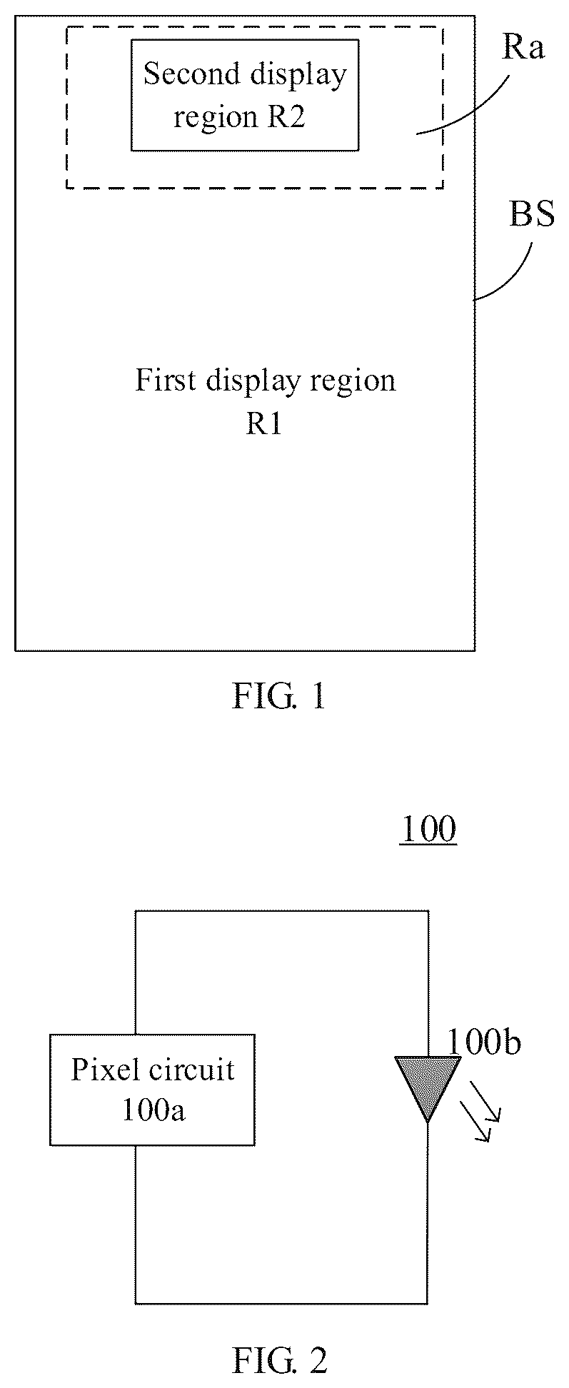
is a schematic structural diagram of a display panel provided by an embodiment of the present disclosure. As illustrated in , the display panel includes a base substrate BS. The display panel includes a first display region R 1 and a second display region R 2 , and the first display region R 1 may be located on at least one side of the second display region R 2 . For example, in some embodiments, the first display region R 1 surrounds the second display region R 2 . That is, the second display region R 2 may be surrounded by the first display region R 1 . The second display region R 2 can also be arranged at other positions, and the arrangement position of the second display region R 2 can be determined according to needs. For example, the second display region R 2 may be located at the top middle position of the base substrate BS, or may be located at the upper left position or the upper right position of the base substrate BS. For example, hardware such as a photosensitive sensor (for example, a camera) is disposed in the second display region R 2 of the display panel. For example, the second display region R 2 is a light-transmitting display region, and the first display region R 1 is a display region. For example, the first display region R 1 is opaque and only used for display.
is a schematic diagram of a pixel unit of a display panel provided by an embodiment of the present disclosure. The display panel includes a pixel unit 100 , and the pixel unit 100 is located on a base substrate. As illustrated in , the pixel unit 100 includes a pixel circuit 100 a and a light-emitting element 100 b , and the pixel circuit 100 a is configured to drive the light-emitting element 100 b . For example, the pixel circuit 100 a is configured to provide a driving current to drive the light-emitting element 100 b to emit light. For example, the light-emitting element 100 b is an organic light-emitting diode (OLED), and the light-emitting element 100 b emits red light, green light, blue light, or white light under the driving of its corresponding pixel circuit 100 b . The light-emitting color of the light-emitting element 100 b can be determined according to needs.
In order to increase the light transmittance of the second display region R 2 , only light-emitting elements may be disposed in the second display region R 2 , and pixel circuits for driving the light-emitting elements of the second display region R 2 may be disposed in the first display region R 1 . That is, the light transmittance of the second display region R 2 is improved by the way that the light-emitting elements and the pixel circuits are separately disposed.
is a schematic diagram of a display panel provided by an embodiment of the present disclosure. As illustrated in , the display panel includes a plurality of first pixel circuits 10 , a plurality of second pixel circuits 20 , and a plurality of first light-emitting elements 30 located in a first display region R 1 , and a plurality of second light-emitting elements 40 located in a second display region R 2 . For example, the plurality of second pixel circuits 20 may be distributed among the plurality of first pixel circuits 10 at intervals.
For example, as illustrated in , at least one first pixel circuit 10 of the plurality of first pixel circuits 10 is connected to at least one first light-emitting element 30 of the plurality of first light-emitting elements 30 , and an orthographic projection of the at least one first pixel circuit 10 on the base substrate BS at least partially overlaps with an orthographic projection of the at least one first light-emitting element 30 on the base substrate BS. The at least one first pixel circuit 10 can be used to provide a driving signal for the connected first light-emitting element 30 to drive the first light-emitting element 30 to emit light.
For example, as illustrated in , at least one second pixel circuit 20 of the plurality of second pixel circuits 20 is connected to at least one second light-emitting element 40 of the plurality of second light-emitting elements 40 through a conductive line L 1 , and the at least one second pixel circuit 20 can be used to provide a driving signal for the connected second light-emitting element 40 to drive the second light-emitting element 40 to emit light. As illustrated in , because the second light-emitting element 40 and the second pixel circuit 20 are located in different regions, there is no overlap between an orthographic projection of the at least one second pixel circuit 20 on the base substrate BS and an orthographic projection of the at least one second light-emitting element 40 on the base substrate BS.
For example, in the embodiments of the present disclosure, the first display region R 1 can be set as an opaque display region, and the second display region R 2 can be set as a light-transmitting display region. For example, the first display region R 1 cannot transmit light, and the second display region R 2 can transmit light. In this way, the display panel provided by the embodiment of the present disclosure does not need to perform drilling processing on the display panel, and the required hardware structure such as the photosensitive sensor can be directly arranged at a position corresponding to the second display region R 2 on one side of the display panel, which lays a solid foundation for the realization of a true full screen. In addition, because the second display region R 2 only includes light-emitting elements and does not include pixel circuits, it is beneficial to increase the light transmittance of the second display region R 2 , so that the display panel has a better display effect.
As illustrated in , the pixel unit 100 includes a first pixel unit 101 and a second pixel unit 102 . A pixel circuit 100 a and a light-emitting element 100 b of the first pixel unit 101 are both located in the first display region R 1 , a pixel circuit 100 a of the second pixel unit 102 is located in the first display region R 1 , and a light-emitting element 100 b of the second pixel unit 102 is located in the second display region R 2 . In the embodiments of the present disclosure, the pixel circuit 100 a of the first pixel unit 101 is the first pixel circuit 10 , the light-emitting element 100 b of the first pixel unit 101 is the first light-emitting element 30 , the pixel circuit 100 a of the second pixel unit 101 is the second pixel circuit 20 , and the light-emitting element 100 b of the second pixel unit 102 is the second light-emitting element 40 . For example, the first light-emitting element 30 may be referred to as an in-situ light-emitting element. For example, the first pixel circuit 10 may be referred to as an in-situ pixel circuit, and the second pixel circuit 20 may be referred to as an ex-situ pixel circuit.
For example, as illustrated in , the second light-emitting element 40 and the second pixel circuit 20 connected to the second light-emitting element 40 are located in the same row. That is, the light-emitting signal of the second light-emitting element 40 comes from the second pixel circuit in the same row. For example, pixel circuits of pixel units in the same row are connected to the same gate line.
As illustrated in , the pixel circuit (the second pixel circuit 20 ) of the second pixel unit 102 is connected to the light-emitting element (the second light-emitting element 40 ) of the second pixel unit 102 through the conductive line L 1 . For example, the conductive line L 1 is made of a transparent conductive material. For example, the conductive line L 1 is made of conductive oxide material. For example, the conductive oxide material includes indium tin oxide (ITO), but is not limited thereto.
As illustrated in , one end of the conductive line L 1 is connected to the second pixel circuit 20 , and the other end of the conductive line L 1 is connected to the second light-emitting element 40 . As illustrated in , the conductive line L 1 extends from the first display region R 1 to the second display region R 2 .
As illustrated in and , in some embodiments, the display panel further includes an auxiliary region Ra, and the auxiliary region Ra can be provided with the second pixel circuit 20 that is connected to the second light-emitting element in the second display region R 2 .
is a schematic diagram of the first display region and the second display region in the display panel provided by an embodiment of the present disclosure. As illustrated in , in the second display region R 2 , a light-transmitting region R 0 is disposed between adjacent second light-emitting elements 40 . For example, as illustrated in , a plurality of light-transmitting regions R 0 are connected to each other to form a continuous light-transmitting region separated by a plurality of second light-emitting elements 40 . The conductive wire L 1 is made of a transparent conductive material to increase the light transmittance of the light-transmitting region R 0 as much as possible. As illustrated in , the region of the second display region R 2 except for the second light-emitting element 40 may be a light-transmitting region.
A to E are partial plan views of a display panel provided by an embodiment of the present disclosure. A to E are described below.
A is a schematic diagram of a first display region and a second display region of a display panel provided by an embodiment of the present disclosure. As illustrated in A , the second display region R 2 is a light-transmitting display region, and the first display region R 1 is a display region.
B is a schematic diagram of a first light-emitting element in a first display region and a second light-emitting element in a second display region of a display panel provided by an embodiment of the present disclosure. B illustrates the first light-emitting element 30 and the second light-emitting element 40 .
Referring to A , B , and , in order to improve the display effect, the density of the second light-emitting element 40 may be equal to the density of the first light-emitting element 30 . That is, the resolution of the second display region R 2 is the same as the resolution of the first display region R 1 . Of course, in other embodiments, the density of the second light-emitting element 40 may be greater or less than the density of the first light-emitting element 30 . That is, the resolution of the second display region R 2 may be greater or less than the resolution of the first display region R 1 . For example, as illustrated in B and , the light-emitting area of the second light-emitting element 40 is smaller than the light-emitting area of the first light-emitting element 30 . illustrates the light-emitting area of the second light-emitting element 40 and the light-emitting area of the first light-emitting element 30 with broken lines. For example, the light-emitting area of a light-emitting element may correspond to the area of the opening of a pixel definition layer.
C is a schematic diagram of conductive lines in a display panel provided by an embodiment of the present disclosure. C illustrates a plurality of conductive lines L 1 .
D is a schematic diagram of conductive lines in a display panel provided by an embodiment of the present disclosure. D illustrates the conductive line L 1 . As illustrated in D , the conductive line L 1 includes a first conductive line L 11 , a second conductive line L 12 , and a third conductive line L 13 . In a display panel with a high PPI, in order to avoid too dense conductive lines, a plurality of conductive line pattern layers may be formed, and an insulating layer is arranged between the different conductive line pattern layers. For example, the first conductive line L 11 is located in a first conductive line pattern layer, the second conductive line L 12 is located in a second conductive line pattern layer, and the third conductive line L 13 is located in a third conductive line pattern layer. Of course, in other embodiments, a plurality of conductive lines in other forms can also be provided. For example, one conductive line L 1 is formed by several conductive parts located in different conductive line pattern layers. For example, the several conductive parts located in different conductive line pattern layers may be connected to one another through via holes penetrating an insulating layer.
E illustrates the first light-emitting element 30 , the second light-emitting element 40 , the first pixel circuit 10 , the second pixel circuit 20 , a connecting element CE 0 , and the conductive line L 1 . Each pixel circuit is connected to a light-emitting element through a connecting element CE 0 . That is, each pixel unit has one connection element CE 0 . That is, the first pixel circuit 10 is connected to the first light-emitting element 30 through the connecting element CE 0 , and the second pixel circuit 20 is connected to the second light-emitting element 40 through the connecting element CE 0 . For example, one end of the conductive line L 1 is connected to the second pixel circuit 20 through the connecting element CE 0 , and the other end of the conductive line L 1 is connected to the second light-emitting element 40 .
As illustrated in E , one conductive line L 1 passes through the region where the pixel circuit of the pixel unit is located to respectively connect the second pixel circuit 20 and the second light-emitting element 40 on both sides of the pixel unit. For example, the region where the pixel circuit of the pixel unit is located overlaps with a plurality of conductive lines L 1 passing through the region, so that the pixel circuit and the conductive lines overlapping with the pixel circuit are coupled to form a parasitic capacitance, which causes a difference in brightness to form a display defect such as stripes (Mura). The region in the first display region R 1 where the second pixel circuit 20 connected to the second light-emitting element 40 is disposed can be called the auxiliary region Ra (as illustrated in and ), and the auxiliary region Ra can also be called a transition region, due to the coupling of the conductive line and the pixel circuit, the auxiliary region (transition region) tends to have darker brightness, and the darker pixel unit is the pixel unit (first pixel unit) in the first display region R 1 , not the second light-emitting element 40 in the second display region R 2 . For example, the case of that the auxiliary region is darker is more obvious in the case of high gray scale than in the case of low gray scale. In E , one first pixel circuit 10 overlaps with two conductive lines L 1 at most as an example. In other embodiments, one first pixel circuit 10 may also overlap with more conductive lines L 1 . For example, as illustrated in C , in some embodiments, one first pixel circuit 10 may overlap with 10-15 conductive lines L 1 . How many conductive lines L 1 overlap with one first pixel circuit 10 can be determined according to needs.
In some embodiments, the size of the first pixel circuit 10 can be compressed in the first direction X to obtain the region where the second pixel circuit 20 is disposed. For example, as illustrated in E , in the auxiliary region, one column of second pixel circuits 20 is arranged every other predetermined column of first pixel circuits 10 . For example, the number of columns of first pixel circuits 10 between two adjacent columns of second pixel circuits 20 can be determined according to needs.
is a schematic diagram of data lines in a display panel. is a schematic diagram of mura of a display panel. is a schematic diagram of data lines in a display panel. A is a schematic diagram of a display panel provided by an embodiment of the present disclosure. B is a schematic diagram of a display panel provided by another embodiment of the present disclosure. C is a schematic diagram of a display panel provided by another embodiment of the present disclosure. A is a schematic diagram of a display panel provided by an embodiment of the present disclosure. B is a schematic diagram of a display panel provided by another embodiment of the present disclosure. - B illustrate the center line a 0 of the display panel. For example, the center line a 0 extends in the second direction Y. For example, the center line a 0 is parallel with the second direction Y. For example, the display panel is symmetrically arranged with respect to the center line a 0 . - C take that the second display region R 2 is located at one side of the first display region R 1 as an example, and A - B take that the first display region R 1 surrounds the second display region R 2 as an example.
As illustrated in , the second display region R 2 is a light-transmitting display region. Referring to and , the second pixel circuit 20 is separated from the second light-emitting element 40 , the second pixel circuit 20 is disposed in the first display region R 1 , and the data line of the second pixel unit 102 (see ) are formed in segments. That is, as illustrated in , the data line DTn includes a first portion DT 01 , a second portion DT 02 and a third portion DT 03 . As illustrated in , the first portion DT 01 and the second portion DT 02 both extend in the second direction Y, the third portion DT 03 extends in the first direction X, and the first portion DT 01 and the second portion DT 02 are connected through the third portion DT 03 . The extending direction of the third portion DT 03 is different from the extending direction of the first portion DT 01 , and the extending direction of the third portion DT 03 is different from the extending direction of the second portion DT 02 , and the third portion DT 03 is located in the display region R 0 . The third portion DT 03 is located in the first display region R 1 . The data line DTn includes a vertical part and a horizontal part, and the length of the data line DTn is greater than the length of the data line DTm of the first pixel unit 101 (see ), so that the loading of the data line DTn is greater than the loading of the data line DTm. And thus, as illustrated in , the display panel has mura of a dark vertical stripe during display. illustrates the dark vertical stripe MR. In the embodiments of the present disclosure, the data lines can be divided into a data line DTm and a data line DTn, the data line DTm can be referred to as a first-type data line DTm, and the data line DTn can be referred to as a second-type data line DTn. For example, the first-type data line DTm extends in the second direction Y, and the second-type data line DTn includes both a part extending in the first direction X and a part extending in the second direction Y. For example, in the embodiments of the present disclosure, the first direction X is the row direction of the pixel units and the second direction Y is the column direction of the pixel units, but it is not limited to this case.
For example, in some embodiments, no metal line is provided in the second display region R 2 , but it is not limited to this case. For example, in some other embodiments, metal lines can also be provided in the second display region R 2 . The structure in the second display region R 2 can be set as needed.
As illustrated in , the display panel includes a display region R 0 and a peripheral region R 3 , and the display region R 0 includes a first display region R 1 and a second display region R 2 . In other words, the base substrate BS has a display region R 0 and a peripheral region R 3 , and the peripheral region R 3 is located on at least one side of the display region R 0 . The peripheral region R 3 is a non-display region.
For example, referring to and , the pixel unit 100 is located on the base substrate BS and includes a pixel circuit 100 a and a light-emitting element 100 b , the pixel circuit 100 a is configured to drive the light-emitting element 100 b , the pixel circuit 100 b includes a driving transistor T 1 (see A ) and a data writing transistor T 2 (see A ), and the driving transistor T 1 and the data writing transistor T 2 are connected to each other.
For example, referring to A and B , the data line DT is connected to the data writing transistor T 2 and is configured to provide a data signal to the pixel circuit 100 a.
For example, in a display panel provided by some embodiments of the present disclosure, as illustrated in A and B , the display panel includes a compensation structure 80 , the compensation structure 80 is connected to the data line DT and located in the peripheral region R 3 , and the compensation structure 80 includes at least one selected from the group consisting of a resistance compensation unit and a capacitance compensation unit. The embodiments of the present disclosure are illustrated by taking that the compensation structure 80 includes both a resistance compensation unit and a capacitance compensation unit as an example.
In the display panel provided by the embodiments of the present disclosure, by arranging the compensation structure, the capacitance/resistance difference between data lines can be reduced, so as to alleviate mura, and alleviate or avoid the occurrence of the dark vertical stripe during display. For example, in the display panel provided by the embodiments of the present disclosure, by arranging the compensation structure, the capacitance/resistance difference between the first-type data lines DTm can be reduced, the capacitance/resistance difference between the second-type data lines DTn can be reduced, and the capacitance/resistance difference between the first-type data line DTm and the second-type data line DTn can be reduced.
For example, when arranging the compensation structure, the compensation amount of each data line can be determined according to the data line with the largest loading in the display panel before compensation. For example, in the display panel provided by some embodiments of the present disclosure, the loading difference between the data lines is small due to the compensation structure.
As illustrated in A , the second-type data line DTn of the display panel is connected to the compensation structure 80 . As illustrated in B , one second-type data line DTn of the display panel is connected to one compensation structure 80 (second compensation structure 82 ).
As illustrated in B , one first-type data line DTm of the display panel is connected to one compensation structure 80 (first compensation structure 81 ). For example, the compensation amount of the first compensation structure 81 is different from the compensation amount of the second compensation structure 82 . For example, the compensation amount of the first compensation structure 81 is greater than the compensation amount of the second compensation structure 82 . For example, the compensation amount of the capacitance of the first compensation structure 81 is different from the compensation amount of the capacitance of the second compensation structure 82 .
For example, the compensation amount of the capacitance of the first compensation structure 81 is greater than the compensation amount of the capacitance of the second compensation structure 82 . For example, the compensation amount of the resistance of the first compensation structure 81 is greater than the compensation amount of the resistance of the second compensation structure 82 . For example, the compensation amount of the capacitance of the first compensation structure 81 is greater than the compensation amount of the second compensation structure 82 , and the compensation amount of the resistance of the first compensation structure 81 is greater than the compensation amount of the resistance of the second compensation structure 82 .
For example, in some embodiments, as illustrated in B , for a plurality of first-type data lines DTm located at one side of the center line a 0 , each first-type data line DTm is connected to one first compensation structure 81 , so that a plurality of first compensation structures 81 are sequentially arranged. For example, the plurality of first compensation structures 81 are arranged in the first direction X. For example, in some embodiments, the first-type data line DTm with the largest capacitance before the compensation structures are provided may not be provided with a compensation structure.
The display panel illustrated in B is a rectangular display panel. For example, as illustrated in B , considering the unequal lengths of data lines in the fan-out region FR (refer to ), the closer the first compensation structure 81 is to the center line a 0 , the compensation amount thereof is greater. That is, the compensation amount of the first compensation structure 81 (the first compensation structure 811 ) close to the center line a 0 is greater than the compensation amount of the first compensation structure 81 (the first compensation structure 811 ) away from the center line a 0 .
For example, in some embodiments, as illustrated in B , for the plurality of first-type data lines DTm located at one side of the center line a 0 , with respect to the edge of the display panel, the compensation amount of the first compensation structure 81 closer to the edge of the display panel is smaller. That is, the compensation amount of the first compensation structure 81 (the first compensation structure 811 ) close to the edge of the display panel is less than the compensation amount of the first compensation structure 81 (the first compensation structure 811 ) away from the edge of the display panel.
For example, as illustrated in B , for the plurality of second-type data lines DTn located at one side of the center line a 0 , each second-type data line DTn is connected to one second compensation structure 82 , so that the plurality of second compensation structures 82 are arranged in the first direction X.
For example, as illustrated in B , the longer the length of the third portion DT 03 of the second-type data line DTn, the greater the loading of the data line, and the smaller the compensation amount of the compensation structure.
For example, as illustrated in B , the farther the distance between the first portion DT 01 of the second-type data line DTn and the center line a 0 , the smaller the compensation amount of the compensation structure of the data line.
The display panel illustrated in C is a display panel with rounded corners. As illustrated in C , the number of data lines at the positions corresponding to rounded corners is less than that of pixel units at other positions, and therefore, for the plurality of first-type data lines DTm located at one side of the center line a 0 , with respect to the edge of the display panel, the closer the first compensation structure 81 is to the edge of the display panel, the greater the compensation amount of the first compensation structure 81 is. That is, the compensation amount of the first compensation structure 81 (the first compensation structure 811 ) close to the edge of the display panel is greater than the compensation amount of the first compensation structure 81 (the first compensation structure 811 ) away from the edge of the display panel.
D is a schematic diagram of part of compensation structures in the display panel illustrated in B or C . D merely illustrates the compensation structures (second compensation structures 82 ) of the second-type data lines DTn, and the arranging of the compensation amount of the compensation structures (first compensation structures 81 ) of the first-type data lines DTm can refer to the above description. As illustrated in B and D , the compensation amount of the second compensation structure 821 is less than the compensation amount of the second compensation structure 822 . For example, in the display panel illustrated in B , at one side of the center line a 0 , the compensation amount of the compensation structure 80 (the second compensation structure 82 ) of the second-type data line DTn gradually changes, and for example, gradually increases or decreases in the first direction X. That is, at one side of the center line a 0 , the compensation amount of the compensation structure 80 (the second compensation structure 82 ) gradually increases in a direction from a position away from the center line a 0 to a position close to the center line a 0 . In some other embodiments, at one side of the center line a 0 , the compensation amount of the compensation structure 80 (the second compensation structure 82 ) of the second-type data line DTn can also gradually decrease in the direction from the position away from the center line a 0 to the position close to the center line a 0 . The arranging trend of the compensation amount of the compensation structure 80 (the second compensation structure 82 ) is related to the length of the third portion DT 3 .
In the embodiments of the present disclosure, the compensation amount of the compensation structure of the second-type data line DTn is inversely proportional to the length of the third portion DT 3 of the second-type data line DTn, that is, the longer the length of the third portion DT 3 , the smaller the compensation amount of the compensation structure connected to the second-type data line DTn, so that the capacitance difference between data lines DT is smaller and the loading difference between data lines DT is smaller. Among the plurality of second-type data lines DTn, in the case where the length of the third portion DT 3 gradually increases, the compensation amount of the compensation structure connected to the second-type data line DTn gradually decreases; and in the case where the length of the third portion DT 3 gradually decreases, the compensation amount of the compensation structure connected to the second-type data line DTn gradually increases.
For example, in the embodiments of the present disclosure, the compensation amount of the compensation structure includes the compensation amount of the capacitance and/or the compensation amount of the resistance. In the case where the capacitance of each data line varies greatly, the capacitance is mainly compensated.
As illustrated in A and B , the first display region R 1 surrounds the second display region R 2 , and the second compensation structure 82 is located at the position of the peripheral region R 3 directly facing the second display region R 2 . For the part of the display panel located at one side of the center line a 0 , a plurality of first compensation structures 81 are adjacent to each other, a plurality of second compensation structures 82 are adjacent to each other, the plurality of first compensation structures 81 are located at one side of the plurality of second compensation structures 82 , and the plurality of second compensation structures 82 are closer to the center line a 0 than the plurality of first compensation structures 81 are. While in the display panels illustrated in - C , the second compensation structures 82 are located outside the position of the peripheral region R 3 directly facing the second display region R 2 , and a plurality of second compensation structures 82 are distributed at intervals among the plurality of first compensation structures 81 . A and B takes that the closer the second portion DT 02 of the second-type data line DTn is to the center line a 0 , the larger the length of the third portion DT 03 of the second-type data line DTn is as an example. In some other embodiments, it can be set that the closer the second portion DT 02 of the second-type data line DTn is to the center line a 0 , the smaller the length of the third portion DT 03 of the data line DTn is.
For example, the capacitance compensation unit includes at least one compensation capacitor, so as to compensate the capacitance of the data line connected thereto.
For example, the capacitance compensation unit includes a plurality of compensation capacitors, and the plurality of compensation capacitors are connected in parallel to increase the compensation amount of the capacitors.
illustrates a schematic layout diagram of a compensation unit provided by an embodiment of the present disclosure. is a cross-sectional view taken along line A 1 -B 1 of . A is a plan view of a first conductive layer in . B is a plan view of a second conductive layer in . C is a plan view of a third conductive layer in . D is a plan view of a fourth conductive layer in . E is a plan view of via holes in . F is a plan view of via holes penetrating at least one of a first insulating layer, a second insulating layer, and a third insulating layer in . G is a plan view of via holes penetrating a fourth insulating layer and a fifth insulating layer in . The display panel illustrated in is illustrated by taking that one data line DT is connected to one compensation structure 80 as an example, and the embodiments of the present disclosure include but are not limited to this case. In some other embodiments, one data line DT can also be connected to a plurality of compensation structures 80 .
For example, the compensation capacitor includes a compensation portion connected to the data line, and at least one compensation electrode-plate that forms the compensation capacitor with the compensation portion. For example, the compensation portion can be at least one of the first compensation portion 801 and the second compensation portion 803 described later. For example, the compensation electrode-plate can be at least one of the first electrode-plate 802 and the second electrode-plate 804 described later.
For example, referring to , A and C , the compensation structure 80 includes a resistance compensation unit, the resistance compensation unit includes a first compensation portion 801 connected to the data line DT and a second compensation portion 803 connected to the first compensation portion 801 . Referring to and , the first compensation portion 801 and the second compensation portion 803 are located in different layers, and the orthographic projection of the first compensation portion 801 on the base substrate BS at least partially overlaps with the orthographic projection of the second compensation portion 803 on the base substrate BS. The first compensation portion 801 and the second compensation portion 803 extend the length of the data line and compensate the resistance of the data line.
For example, as illustrated in and E , the first compensation portion 801 is in contact with the second compensation portion 803 . For example, the first compensation portion 801 and the second compensation portion 803 are connected through a via hole V 1 penetrating the third insulating layer ISL 3 and the second insulating layer ISL 2 .
For example, referring to , and A - D , the compensation structure includes a capacitance compensation unit, and the capacitance compensation unit includes a first compensation portion 801 , a first electrode-plate 802 , a second compensation portion 803 , and a second electrode-plate 804 . The first compensation portion 801 is connected to the data line, the first compensation portion 801 is located in a first conductive layer LY 1 , the first electrode-plate 802 is located in a second conductive layer LY 2 , the second compensation portion 803 is located in a third conductive layer LY 3 , the second electrode-plate 804 is located in a fourth conductive layer LY 4 , the first conductive layer LY 1 is located on a first insulating layer ISL 1 , a second insulating layer ISL 2 is disposed between the first conductive layer LY 1 and the second conductive layer LY 2 , a third insulating layer ISL 3 is disposed between the second conductive layer LY 2 and the third conductive layer LY 3 , and an insulating layer ISL 0 is disposed between the third conductive layer LY 3 and the fourth conductive layer LY 4 . For example, the insulating layer ISL 0 includes a fourth insulating layer ISL 4 and a fifth insulating layer ISL 5 , or the insulating layer ISL 0 includes only one of the fourth insulating layer ISL 4 and the fifth insulating layer ISL 5 . The first insulating layer ISL 1 can also be referred to as a first gate insulating layer. The second insulating layer ISL 2 can also be referred to as a second gate insulating layer. The third insulating layer ISL 3 can also be referred to as an interlayer dielectric layer. The fourth insulating layer ISL 4 can also be referred to as a passivation layer. The fifth insulating layer ISL 5 can also be referred to as a planarization layer.
For example, in the case where the display substrate provided by the embodiments of the present disclosure includes a capacitance compensation unit, the compensation effect is better, which is more conducive to alleviating or eliminating mura. For example, in some embodiments, the patterns of the first electrode-plate 802 and the second electrode-plate 804 are the same, but they are not limited to this case, and can be set as needed. For example, the second electrode-plate 804 is located in the same layer as the shield electrode SE mentioned later. That is, both of the second electrode-plate 804 and the shield electrode SE are located in the fourth conductive layer LY 4 . For example, the first to fourth conductive layers LY 1 -LY 4 illustrated in and are the first to fourth conductive layers LY 1 -LY 4 in the display panels illustrated in B - E , G , H and , respectively. The entire structure of the display panel is not illustrated in each drawing.
For example, referring to , , A and C , the first compensation portion 801 and the second compensation portion 803 form a resistance compensation unit.
For example, one compensation structure may correspond to one capacitance compensation unit, and one compensation structure may correspond to one resistance compensation unit.
For example, referring to , , A and C , the orthographic projection of the first compensation portion 801 on the base substrate BS at least partially overlaps with the orthographic projection of the second compensation portion 803 on the base substrate BS.
For example, the width of the first compensation portion 801 in the first direction X is the same as the width of the second compensation portion 803 in the first direction X. The first direction X intersects with the extending direction of the first compensation portion 801 and intersects with the extending direction of the second compensation portion 803 . For example, the first direction X is perpendicular to the extending direction of the first compensation portion 801 and is perpendicular to the extending direction of the second compensation portion 803 , but it is not limited to this case.
For example, as illustrated in , the first compensation portion 801 and the second compensation portion 803 are connected through a via hole V 1 penetrating both the third insulating layer ISL 3 and the second insulating layer ISL 2 , so as to facilitate the formation of the resistance compensation unit and the capacitance compensation unit.
For example, the first compensation portion 801 overlaps with the first electrode-plate 802 to form a first compensation capacitor C 1 , the second compensation portion 803 overlaps with the first electrode-plate 802 to form a second compensation capacitor C 2 , the second compensation portion 803 overlaps with the second electrode-plate 804 to form a third compensation capacitor C 3 , and the first compensation capacitor C 1 , the second compensation capacitor C 2 , and the third compensation capacitor C 3 are connected in parallel to increase the compensation amount of capacitance.
For example, referring to and C , the third conductive layer LY 3 further includes a signal line SL 3 , the signal line SL 3 extends in the first direction X, and the orthographic projection of the signal line SL 3 on the base substrate partially overlaps with the orthographic projection of the first compensation portion 801 on the base substrate.
For example, referring to and C , the third conductive layer LY 3 further includes a signal line SL 4 , the signal line SL 4 extends in the first direction X, and the orthographic projection of the signal line SL 4 on the base substrate partially overlaps with the orthographic projection of the first compensation portion 801 on the base substrate.
For example, one of the signal line SL 3 and the signal line SL 4 is a high-level signal line, and the other of the signal line SL 3 and the signal line SL 4 is a low-level signal line. Neither the signal line SL 3 nor the signal line SL 4 is connected to the data line DT. The high-level signal line is configured to provide a high level, the low-level signal line is configured to provide a low level, and the voltage of the high level is greater than the voltage of the low level.
For example, referring to , and B , in order to facilitate manufacturing and the compensation of capacitance, the first electrode-plates 802 of the plurality of compensation structures are integrally formed as an integrated structure, and the second electrode-plates 804 of the plurality of compensation structures are integrally formed as an integrated structure.
For example, in order to facilitate the compensation of capacitance, both the first electrode-plate 802 and the second electrode-plate 804 are connected to a constant voltage terminal. For example, as illustrated in A , the constant voltage terminal includes at least one of a first power terminal TM 1 and a second power terminal TM 2 . For example, the first power terminal TM 1 is connected to a first power supply line PL 1 illustrated in A , and the second power terminal TM 2 is connected to a second power supply line PL 2 illustrated in A .
For example, as illustrated in A and B , the display region R 0 includes a first display region R 1 and a second display region R 2 . The first display region R 1 is located on at least one side of the second display region R 2 , and the data line DT is not located in the second display region R 2 .
Referring to and C , the display panel includes a first connection structure 831 . Referring to and E , the first connection structure 831 is connected to the first compensation portion 801 through a via hole V 2 , and the data line DT is connected to the first connection structure 831 through a via hole V 3 . For example, referring to and F , the via hole V 2 is configured to connect structures in the first conductive layer LY 1 and the third conductive layer LY 3 , so that the via hole V 2 penetrates both the third insulating layer ISL 3 and the second insulating layer ISL 2 . For example, referring to and G , the via hole V 3 is configured to connect structures in the fourth conductive layer LY 4 and the third conductive layer LY 3 , so that the via hole V 3 penetrates both the fourth insulating layer ISL 4 and the fifth insulating layer ISL 5 . Similarly, the via hole V 5 also penetrates both the fourth insulating layer ISL 4 and the fifth insulating layer ISL 5 . For example, in some embodiments, the data line DT includes portions located in different layers. In some embodiments, the data line DT includes a portion located in the fourth conductive layer LY 4 and a portion located in the third conductive layer LY 3 . In some embodiments, the third portion DT 03 of the data line DT can be located in the second conductive layer LY 2 , but it is not limited thereto. For example, in some embodiments, the first connection structure 831 may not be provided, and the first portion DT 01 of the data line is connected to the first compensation portion 801 through a via hole.
Referring to and A , the display panel includes a signal line SL 2 . Referring to and C , the display panel includes a signal line 841 , and the signal line 841 is connected to the signal line SL 2 . For example, the signal line 841 can be the first power supply line PL 1 mentioned later, but it is not limited thereto. Referring to and E , the signal line 841 is connected to the signal line SL 2 through a via hole V 5 .
Referring to and B , the display panel includes a signal line SL 1 . Referring to and C , the display panel includes a signal line 832 , and the signal line 832 is connected to the signal line SL 1 . For example, the signal line 832 can be an initialization signal line mentioned later, but it is not limited thereto. Referring to and E , the signal line 832 is connected to the signal line SL 1 through a via hole V 4 . For example, the via hole V 4 is configured to connect the signal line 832 in the third conductive layer LY 3 and the signal line SL 1 in the second conductive layer LY 2 , and therefore, the via hole V 4 penetrates the third insulating layer ISL 3 .
Referring to and C , the display panel includes a signal line SL 9 . As illustrated in C , the signal line SL 9 is located in the third conductive layer LY 3 . Referring to and B , the display panel further includes signal lines SL 5 to SL 8 . As illustrated in B , the signal lines SL 5 to SL 8 are located in the second conductive layer LY 2 . For example, the signal lines SL 5 to SL 9 can be crack detection lines, but not limited thereto. It should be noted that the number and position of crack detection lines in the display panel are not limited to those illustrated in the figure, but can be set as needed. Of course, the display panel may not be provided with crack detection lines.
It should be noted that the embodiments of the present disclosure are illustrated by taking the display panel illustrated in as an example. Those skilled in the art can make changes and modifications based on the description of to obtain novel embodiments. For example, on the basis of the display panel illustrated in , it is possible to adjust the layer in which an element is disposed, and to add or remove part of signal lines, etc.
A - G are schematic diagrams of compensation structures in some display panels provided by some embodiments of the present disclosure. H is a schematic diagram of a compensation structure in a display panel provided by an embodiment of the present disclosure. I is a schematic diagram of a compensation structure in a display panel provided by an embodiment of the present disclosure. J is an enlarged schematic diagram of the compensation structures in I .
Compared with the display panel illustrated in , the display panel illustrated in A retains the compensation structure 80 , but removes the signal lines SL 1 -SL 9 and the structures connected to the signal lines. That is, in the display panel provided by the embodiments of the present disclosure, the arrangement of the surrounding structure of the compensation structure 80 may not adopt the situation illustrated in .
Compared with the display panel illustrated in , in the display panel illustrated in B , one data line DT is connected to three compensation structures 80 . Of course, the number of compensation structures 80 connected to one data line DT is not limited in the embodiments of the present disclosure, and one data line DT can be connected to one compensation structure 80 or one data line DT can be connected to a plurality of compensation structures 80 . In the case where one data line DT is connected to a plurality of compensation structures 80 , the capacitors of the plurality of compensation structures are connected in parallel, which can further increase the total capacitance of the compensation structures connected to the data line.
Compared with the display panel illustrated in B , the display panel illustrated in C retains the compensation structure 80 , while the signal lines SL 1 -SL 9 and the structures connected to the signal lines are removed. That is, in the display panel provided by the embodiments of the present disclosure, the arrangement of the surrounding structure of the compensation structure 80 may not adopt the situation illustrated in .
As illustrated in D , the compensation amount of the compensation structure 80 can be adjusted by adjusting the size of the first electrode-plate 802 or the second electrode-plate 804 in the second direction Y. As illustrated in D , in two compensation structures 80 with different compensation amounts, the first compensation portions 801 have the same size and have the same shape, and the second compensation portions 803 have the same size and have the same shape.
E is a schematic diagram of a display panel provided by an embodiment of the present disclosure. As illustrated in E , the compensation amounts of the compensation structures (compensation units) of different data lines can be different. In some embodiments of the present disclosure, in order to facilitate the arranging of the compensation structure, the data lines can be divided into groups, and the compensation amounts of data lines in one group are the same, but the compensation amounts of data lines in different groups are different. For example, each group of data lines can include at least one data line. For example, the data lines in each group are adjacent data lines. For example, each group of first-type data lines includes a plurality of first-type data lines. For example, each group of second-type data lines includes at least one second-type data line.
F is a schematic diagram of a display panel provided by an embodiment of the present disclosure. G is a schematic diagram of a display panel provided by an embodiment of the present disclosure. As illustrated in F and G , the compensation amount of the compensation structure 80 a (first compensation structure 80 a ) of the first-type data line DTm is different from the compensation amount of the compensation structure 80 b (second compensation structure 80 b ) of the second-type data line DTn. For example, as illustrated in F and G , the compensation amount of the first compensation structure 80 a of the first-type data line DTm is different from the compensation amount of the second compensation structure 80 b of the second-type data line DTn adjacent to the first-type data line DTm. For example, the compensation amount of the first compensation structure 80 a is greater than the compensation amount of the second compensation structure 80 b.
As illustrated in F and G , the second-type data lines DTn includes a data line DTa, a data line DTb, and a data line DTc, and the compensation amount of the second compensation unit 80 b connected to the second-type data line DTn is less than the compensation amount the first compensation unit 80 a connected to the first-type data line DTm. F and G are illustrated by taking that the compensation amounts of the compensation units 80 connected to the data line DTa, the data line DTb, and the data line DTc are the same as an example. In some other embodiments, the compensation amounts of the compensation units 80 connected to the data line DTa, the data line DTb, and the data line DTc can be different. In G , the remaining data lines DT, other than the data line DTa, the data line DTb, and the data line DTc, are first-type data lines DTm.
Compared with the display panel illustrated in F , in the display panel illustrated in G , in two compensation structures 80 with different compensation amounts, the first compensation portions 801 have the same size and have the same shape, and the second compensation portions 803 have the same size and have the same shape. For example, as illustrated in G , in two compensation structures 80 with different compensation amounts, the via holes V 1 are located on a straight line. However, in the display panel illustrated in F , the via holes V 1 are staggered.
In the display panel illustrated in H - J , the orthographic projection of the first electrode-plate 802 on the base substrate at least partially overlaps with the orthographic projection of the second electrode-plate 804 on the base substrate. For example, the orthographic projection of the second electrode-plate 804 on the base substrate falls within the orthographic projection of the first electrode-plate 802 on the base substrate. In some embodiments, the orthographic projection of the first electrode-plate 802 on the base substrate can also coincide with the orthographic projection of the second electrode-plate 804 on the base substrate. In the display panel provided by the embodiments of the present disclosure, in order to facilitate the application of signals, the first electrode-plates 802 of different compensation structures 80 are integrally formed as an integrated structure. For example, in the display panel provided by the embodiments of the present disclosure, in order to facilitate the application of signals, the second electrode-plates 804 of different compensation structures 80 are integrally formed as an integrated structure.
For example, as illustrated in H to J , at one side of the center line a 0 of the display panel, the size of the first electrode-plate 802 in the second direction Y gradually changes. For example, the size of the first electrode-plate 802 in the second direction Y gradually changes in a stepwise manner. As illustrated in H - J , at one side of the center line a 0 of the display panel, the size of the first electrode-plate 802 in the second direction Y gradually decreases from the position away from the center line a 0 to the position close to the center line a 0 . Of course, in some other embodiments, at one side of the center line a 0 of the display panel, the size of the first electrode-plate 802 in the second direction Y can also gradually increase from the position away from the center line a 0 to the position close to the center line a 0 . The second electrode-plate 804 can have the same arranging trend as the first electrode-plate 802 .
As illustrated in H , for the second-type data line DTn, the length of the third portion DT 03 gradually changes. The closer the second portion DT 02 is to the center line a 0 , the greater the length of the third portion DT 03 is. According to that the compensation amount of the compensation structure 82 (second compensation structure 82 ), is inversely proportional to the length of the third portion DT 03 , the closer the second compensation structure 82 is to the center line a 0 , the smaller the compensation amount thereof is.
As illustrated in H - J , the first electrode-plate 802 is symmetrically arranged with respect to the center line a 0 , and the second electrode-plate 804 is symmetrically arranged with respect to the center line a 0 .
As illustrated in A and H , the second display region R 2 is surrounded by the first display region R 1 . The second-type data line DTn further includes a fourth portion DT 04 and a fifth portion DT 05 . The fourth portion DT 04 extends in the second direction Y, the fifth portion DT 05 extends in the first direction X, and the first portion DT 01 and the fourth portion DT 04 are connected through the fifth portion DT 05 . The fifth portion DT 05 is located in the peripheral region R 3 . For example, in some embodiments, the first portion DT 01 and the fourth portion DT 04 are located in the same layer, and the fifth portion DT 05 is not located in the same layer as the first portion DT 01 or the fourth portion DT 04 . For example, in some embodiments, the fifth portion DT 05 is located in the fourth conductive layer or the second conductive layer, and the first portion DT 01 and the fourth portion DT 04 are located in the third conductive layer, but it is not limited to this case.
The layer in which each portion of the second-type data line DTn is located can be set as needed, as long as two portions connected through a via hole are located in different layers. For example, for each portion of the second-type data line DTn, two portions with different extending directions are located in different layers. Of course, other manners can also be adopted. Each of the first portion DT 01 to the fifth portion DT 05 illustrated in the figure can also include sub-portions located in different layers.
As illustrated in A and H , the fifth portion DT 05 is located in the peripheral region R 3 , and the fourth portion DT 04 extends from the display region R 0 to the peripheral region R 3 . As illustrated in A and H , the fourth portion DT 04 extends from one side of the first display region R 1 , opposite to the side of the second display region R 2 where the second portion DT 02 is located, to the peripheral region R 3 .
As illustrated in A and H , the plurality of first-type data lines DTm and first portions DT 01 of the plurality of second-type data lines DTn are arranged at intervals. The number of first-type data lines DTm arranged between adjacent first portions DT 01 is not limited to that illustrated in the figure, but can be set as needed.
For example, in the embodiments of the present disclosure, for the second-type data line DTn, the compensation structure is provided at the position of the peripheral region R 3 corresponding to the fourth portion DT 04 , while the compensation structure of the second-type data line DTn is not provided at the position corresponding to the first portion DT 01 of the second-type data line DTn. For example, at the position corresponding to the first portion DT 01 of the second-type data line DTn, a compensation structure of the first-type data line DTn can be arranged. Of course, in the display panel without the fourth portion DT 04 and the fifth portion DT 05 (as illustrated in A - C ), for the second-type data line DTn, the compensation structure is provided at the position of the peripheral region R 3 corresponding to the first portion DT 01 .
As illustrated in B , C , D , I and J , the display panel further includes a second connection structure 850 , and the data line DT is connected to a plurality of compensation structures 80 through the second connection structure 850 . The second connection structure 850 can include a plurality of branches. For example, each branch is connected to one compensation structure 80 . For example, the second connection structure 850 can be integrated with the portion of the data line DT close the second connection structure 850 , but it is not limited to this case, and the second connection structure 850 can also be located in a different layer from the portion of the data line DT close to the second connection structure 850 . The second connection structure 850 is made of a conductive material. For example, the second connection structure 850 can be located in the first conductive layer LY 1 , the second conductive layer LY 2 , the third conductive layer LY 3 or the fourth conductive layer LY 4 . I does not illustrate the portion of the data line DT located in the first display region R 1 .
In the embodiments of the present disclosure, the compensation amount of the compensation structure can be adjusted by adjusting at least one of the first compensation portion 801 , the first electrode-plate 802 , the second compensation portion 803 or the second electrode-plate 804 . For example, the compensation amount of the compensation structure can be adjusted by adjusting the length and width of the first compensation portion 801 and those of the second compensation portion 803 , or by adjusting the opposing area of the first electrode-plate 802 and the first compensation portion 801 , the opposing area of the first electrode-plate 802 and the second compensation portion 803 , or the opposing area of the second electrode-plate 804 and the second compensation portion 803 .
is a schematic diagram of a display panel provided by an embodiment of the present disclosure. As illustrated in , the compensation structure includes a compensation unit 8001 , a compensation unit 8002 , a compensation unit 8003 , and a compensation unit 8004 . In , the compensation amount of the compensation structure 80 is represented by the length of the compensation structure 80 in the second direction. As illustrated in , the compensation amounts of the compensation structures 80 are different. As illustrated in , the compensation amount of the compensation structure 8002 connected to the second-type data line DTn is less than the compensation amount of either of the compensation structures 8001 , 8003 and 8004 connected to the first-type data lines DTm. As illustrated in , due to the length difference between the data lines in the fan-out region FR, the compensation amount of the compensation structure 8001 is less than the compensation amount of the compensation structure 8003 , and the compensation amount of the compensation structure 8003 is less than the compensation amount of the compensation structure 8004 . For example, for the compensation structure 80 connected to the first-type data line DTm, the closer the first-type data line DTm is to the edge of the display panel, the smaller the compensation amount of the compensation structure 80 connected to the first-type data line DTm; and the closer the first-type data line DTm is to the center line a 0 of the display panel, the greater the compensation amount of the compensation structure 80 connected to the first-type data line DTm.
further illustrates a data selector MO. As illustrated in , one end of a data transmission line DTL is connected to at least two data lines DT through the data selector MO, and the other end of the data transmission line DTL is connected to an integrated circuit IC. The data line DT is configured to input data signals to a plurality of pixel units 100 . The data transmission line DTL can be regarded as a part of the data line DT. For example, the data line DT is configured to input data signals to a column of pixel units 100 . For example, one data transmission line DTL inputs data signals to the data lines DT connected thereto at different time periods through the data selector MO. takes that one data transmission line DTL is connected to two data lines DT through the data selector MO as an example, but it is not limited to this case. illustratively illustrates components such as the data selector MO, the pixel units 100 , the data line DT, the data transmission line DTL, etc. The number of each component is not limited to that illustrated in the figure. illustrates a display region R 1 and a peripheral region R 2 located on at least one side of the display region R 1 . As illustrated in , a plurality of data lines DT are arranged in the first direction X, and each data line DT extends in the second direction Y. The arranging of the data selector MO is beneficial to obtaining a display panel with high frame rate and high refresh rate. As illustrated in , the fan-out region FR is located in the peripheral region R 3 .
For example, the position of the compensation structure 80 in the display panel provided by the embodiments of the present disclosure can be within the dashed border RP illustrated in . Of course, the arranging position of the compensation structure 80 can also be as illustrated in H and I . For example, the data line DT can be formed of multiple portions located in different layers, and the layer in which each portion is located can be set as needed. For example, the first portion DT 01 of the data line DT can be located in the third conductive layer LY 3 . The third portion DT 03 of the data line DT can be located in the second conductive layer LY 2 or the fourth conductive layer LY 4 . The second portion DT 02 of the data line DT can be located in the third conductive layer LY 3 .
For example, as illustrated in , the data line DT extends from the first display region R 1 to the peripheral region R 3 . In some accompanying drawings, only a part of the data lines DT are illustrated, but not all of the data lines. As illustrated in H , for the second-type data line DTn, the fourth portion DT 04 is connected to the compensation structure 80 . As illustrated in A - B , for the second-type data line DTn, the first portion DT 01 is connected to the compensation structure 80 .
For example, referring to , the pixel unit 100 includes a first pixel unit 101 and a second pixel unit 102 . A pixel circuit (first pixel circuit 10 ) and a light-emitting element (first light-emitting element 30 ) of the first pixel unit 101 are both located in the first display region R 1 , a pixel circuit (second pixel circuit 20 ) of the second pixel unit 102 is located in the first display region R 1 , a light-emitting element (second light-emitting element 40 ) of the second pixel unit 102 is located in the second display region R 2 , and the pixel circuit (second pixel circuit 20 ) of the second pixel unit 102 is connected to the light-emitting element (second light emitting element 40 ) of the second pixel unit 102 through a conductive line L 1 . Referring to E , the orthographic projection of the conductive line L 1 on the base substrate BS partially overlaps with the orthographic projection of the pixel circuit (first pixel circuit 10 ) of the first pixel unit 101 on the base substrate BS.
For example, referring to B , the light-emitting area of the first light-emitting element 30 is greater than the light-emitting area of the second light-emitting element 40 , and the resolution of the first display region R 1 is the same as the resolution of the second display region R 2 .
Referring to , - C , A - B , H and , the display panel further includes a dummy data line DM, the dummy data line DM is a disconnected data line, the dummy data line DM is disconnected from the first portion DT 01 of the second-type data line DTn, and the dummy data line DM is located between two first-type data lines DTm and disconnected from the first portion DT 01 of one second-type data line DTn located between the two first-type data lines DTm. A part of the second portion DT 02 of the second-type data line DTn and the third portion DT 03 of the second-type data line DTn are not located between the two first-type data lines DTm. As illustrated in , the dummy data line DM is not connected to the data selector MO. As illustrated in , the dummy data line DM is not connected to the integrated circuit IC. For example, the dummy data line DM can be connected to a constant voltage line, but it is not limited to this case. For example, the pixel circuit overlapping with the dummy data line DM can be a dummy pixel circuit, and the dummy pixel circuit is not connected to a light-emitting element.
As illustrated in D , D and H - J , the orthographic projection of the first electrode-plate 802 on the base substrate partially overlaps with, but do not coincide with, the orthographic projection of the second electrode-plate 804 on the base substrate. Of course, the orthographic projection of the first electrode-plate 802 on the base substrate can also coincide with the orthographic projection of the second electrode-plate 804 on the base substrate in these figures. In the display panels illustrated in other figures, in terms of the compensation structure, the orthographic projection of the first electrode-plate 802 on the base substrate coincide with the orthographic projection of the second electrode-plate 804 on the base substrate, but of course, they can also be set to be non-coincident.
The embodiments of the present disclosure are illustrated by taking that each compensation structure includes three capacitors connected in parallel as an example, but it is not limited to this case, and more capacitors connected in parallel can be arranged as needed. In some other embodiments, each compensation structure can include one or two of three capacitors connected in parallel. That is, as illustrated in , the display panel can include one or two of the first compensation capacitor C 1 , the second compensation capacitor C 2 , and the third compensation capacitor C 3 . For example, the capacitance of the first compensation capacitor C 1 is greater than the capacitance of the third compensation capacitor C 3 , and the capacitance of the second compensation capacitor C 2 is greater than the capacitance of the third compensation capacitor C 3 . For example, the capacitance of the first compensation capacitor C 1 is greater than the capacitance of the second compensation capacitor C 2 . For example, the compensation amount of the compensation capacitor is related to the opposing area of the compensation electrode-plates and the material and thickness of the insulating layer between the compensation electrode-plates.
A is a schematic diagram of a pixel circuit in a display panel provided by an embodiment of the present disclosure. B is a layout diagram of a pixel circuit in a display panel provided by an embodiment of the present disclosure. C is a cross-sectional view taken along line A-B of B . D is a layout diagram of a pixel circuit in a display panel provided by an embodiment of the present disclosure. E is a cross-sectional view taken along line C-D of D . F is a partial schematic diagram of a display panel provided by an embodiment of the present disclosure.
The pixel circuit illustrated in A may be a low temperature polysilicon (LTPS) AMOLED pixel circuit commonly used in the related art.
A illustrates a pixel circuit of one pixel unit of the display panel. As illustrated in A , the pixel unit 100 includes the pixel circuit 100 a and the light-emitting element 100 b . The pixel circuit 100 a includes six switching transistors (T 2 -T 7 ), one driving transistor T 1 , and one storage capacitor Cst. The six switching transistors are respectively a data writing transistor T 2 , a threshold compensation transistor T 3 , a first light-emitting control transistor T 4 , a second light-emitting control transistor T 5 , a first reset transistor T 6 , and a second reset transistor T 7 . The light-emitting element 100 b includes a first electrode E 1 and a second electrode E 2 , and a light-emitting function layer located between the first electrode E 1 and the second electrode E 2 . For example, the first electrode E 1 is an anode, and the second electrode E 2 is a cathode. Generally, the threshold compensation transistor T 3 and the first reset transistor T 6 reduce leakage current by adopting double-gate thin film transistors (TFT).
As illustrated in A , the display panel includes a gate line GT, a data line DT, a first power supply line PL 1 , a second power supply line PL 2 , a light-emitting control signal line EML, an initialization signal line INT, a reset control signal line RST, and the like. For example, the reset control signal line RST includes a first reset control signal line RST 1 and a second reset control signal line RST 2 . The first power supply line PL 1 is configured to provide a constant first voltage signal VDD to the pixel unit 100 , the second power supply line PL 2 is configured to provide a constant second voltage signal VSS to the pixel unit 100 , and the first voltage signal VDD is greater than the second voltage signal VSS. The gate line GT is configured to provide a scan signal SCAN to the pixel unit 100 , the data line DT is configured to provide a data signal DATA (data voltage VDATA) to the pixel unit 100 , the light-emitting control signal line EML is configured to provide a light-emitting control signal EM to the pixel unit 100 , the first reset control signal line RST 1 is configured to provide a first reset control signal RESET 1 to the pixel unit 100 , and the second reset control signal line RST 2 is configured to provide the scan signal SCAN to the pixel unit 100 . The first initialization signal line INT 1 is configured to provide a first initialization signal Vinit 1 to the pixel unit 100 . The second initialization signal line INT 2 is configured to provide a second initialization signal Vinit 2 to the pixel unit 100 . For example, the first initialization signal Vinit 1 and the second initialization signal Vinit 2 are constant voltage signals, and their magnitudes may be between the first voltage signal VDD and the second voltage signal VSS, but are not limited thereto. For example, the first initialization signal Vinit 1 and the second initialization signal Vinit 2 may both be less than or equal to the second voltage signal VSS. For example, in some embodiments, the first initialization signal line INT 1 and the second initialization signal line INT 1 are connected with each other, and are both configured to provide an initialization signal Vinit to the pixel unit 100 , that is, the first initialization signal line INT 1 and the second initialization signal line INT 2 are both referred to as an initialization signal line INT, and the first initialization signal Vinit 1 and the second initialization signal Vinit 2 are equal, and both are Vinit.
As illustrated in A , the driving transistor T 1 is electrically connected to the light-emitting element 100 b , and outputs a driving current to drive the light-emitting element 100 b to emit light under the control of the scan signal SCAN, the data signal DATA, the first voltage signal VDD, and the second voltage signal VSS.
For example, the light-emitting element 100 b includes an organic light emitting diode (OLED), and the light-emitting element 100 b emits red light, green light, blue light, or white light under the driving of its corresponding pixel circuit 100 a . For example, one pixel includes a plurality of pixel units. One pixel may include a plurality of pixel units that emit light of different colors. For example, one pixel includes a pixel unit that emits red light, a pixel unit that emits green light, and a pixel unit that emits blue light, but it is not limited to this. The number of pixel units included in a pixel and the light output of each pixel unit can be determined according to needs.
For example, as illustrated in A , a gate electrode T 20 of the data writing transistor T 2 is connected to the gate line GT, a first electrode T 21 of the data writing transistor T 2 is connected to the data line DT, and a second electrode T 22 of the data writing transistor T 2 is connected to a first electrode T 11 of the driving transistor T 1 .
For example, as illustrated in A , the pixel circuit 100 a further includes the threshold compensation transistor T 3 , a gate electrode T 30 of the threshold compensation transistor T 3 is connected to the gate line GT, a first electrode T 31 of the threshold compensation transistor T 3 is connected to a second electrode T 12 of the driving transistor T 1 , and a second electrode T 32 of the threshold compensation transistor T 3 is connected to a gate electrode T 10 of the driving transistor T 1 .
For example, as illustrated in A , the display panel further includes the light-emitting control signal line EML, and the pixel circuit 100 a further includes the first light-emitting control transistor T 4 and the second light-emitting control transistor T 5 . A gate electrode T 40 of the first light-emitting control transistor T 4 is connected to the light-emitting control signal line EML, a first electrode T 41 of the first light-emitting control transistor T 4 is connected to the first power supply line PL 1 , and a second electrode T 42 of the first light-emitting control transistor T 4 is connected to the first electrode T 11 of the driving transistor T 1 . A gate electrode T 50 of the second light-emitting control transistor T 5 is connected to the light-emitting control signal line EML, a first electrode T 51 of the second light-emitting control transistor T 5 is connected to the second electrode T 12 of the driving transistor T 1 , and a second electrode T 52 of the second light-emitting control transistors T 5 is connected to a first electrode E 1 of the light-emitting element 100 b.
As illustrated in A , the first reset transistor T 6 is connected to the gate electrode T 10 of the driving transistor T 1 and is configured to reset the gate electrode of the driving transistor T 1 , and the second reset transistor T 7 is connected to the first electrode E 1 of the light-emitting element 100 b and is configured to reset the first electrode E 1 of the light-emitting element 100 b . The first initialization signal line INT 1 is connected to the gate electrode of the driving transistor T 1 through the first reset transistor T 6 . The second initialization signal line INT 2 is connected to the first electrode E 1 of the light-emitting element 100 b through the second reset transistor T 7 . For example, the first initialization signal line INT 1 and the second initialization signal line INT 2 are connected to each other and are input with the same initialization signal, but it is not limited to this. In some embodiments, the first initialization signal line INT 1 and the second initialization signal line INT 2 may also be insulated from each other and configured to input signals respectively.
For example, as illustrated in A , a first electrode T 61 of the first reset transistor T 6 is connected to the first initialization signal line INT 1 , a second electrode T 62 of the first reset transistor T 6 is connected to the gate electrode T 10 of the driving transistor T 1 , a first electrode T 71 of the second reset transistor T 7 is connected to the second initialization signal line INT 2 , and a second electrode T 72 of the second reset transistor T 7 is connected to the first electrode E 1 of the light-emitting element 100 b . For example, as illustrated in A , a gate electrode T 60 of the first reset transistor T 6 is connected to the first reset control signal line RST 1 , and a gate electrode T 70 of the second reset transistor T 7 is connected to the second reset control signal line RST 2 .
As illustrated in A , the first power supply line PL 1 is configured to provide the first voltage signal VDD to the pixel circuit 100 a . The pixel circuit further includes the storage capacitor Cst, a first electrode Ca of the storage capacitor Cst is connected to the gate electrode T 10 of the driving transistor T 1 , and a second electrode Cb of the storage capacitor Cst is connected to the first power supply line PL 1 .
For example, as illustrated in A , the display panel further includes the second power supply line PL 2 , and the second power supply line PL 2 is connected to a second electrode 201 of the light-emitting element 100 b.
A illustrates a first node N 1 , a second node N 2 , a third node N 3 , and a fourth node N 4 . For example, in some embodiments, referring to C , E , and A , a capacitor is formed between the first node N 1 and the conductive line L 1 , and a capacitor is formed between the conductive line L 1 and the fourth node N 4 , that is, the conductive line L 1 is coupled with the first node N 1 and the fourth node N 4 , respectively, resulting in brightness differences and display defects (for example, forming stripes (Mura)), which affects the display quality.
As illustrated in B , the pixel circuit includes the driving transistor T 1 , and the driving transistor includes the gate electrode T 10 . Referring to B and C , the second electrode Cb of the storage capacitor Cst has an opening OPN 1 , and one end of the connecting electrode CE 1 is connected to the gate electrode T 10 of the driving transistor T 1 through the opening OPN 1 . The connection electrode CE 1 may also be referred to as a first gate signal line SL 1 . As illustrated in B , the first gate signal line SL 1 is connected to the gate electrode T 10 of the driving transistor T 1 .
As illustrated in B , the first gate signal line SL 1 is connected to the second gate signal line SL 2 . The gate electrode T 10 of the driving transistor T 1 , the first gate signal line SL 1 , and the second gate signal line SL 2 constitute a gate signal portion PT 1 . The potentials on the gate signal portion PT 1 are the same. Of course, in other embodiments, the second gate signal line SL 2 may not be provided, in this case, the gate electrode T 10 of the driving transistor T 1 and the first gate signal line SL 1 constitute the gate signal portion PT 1 . For example, the second gate signal line SL 2 is the second electrode T 62 of the first reset transistor T 6 .
Referring to B and C , in order to stabilize the potentials on the gate signal portion PT 1 , the display panel provided by the embodiment of the present disclosure provides a shield electrode SE and a constant voltage line L 0 , and the constant voltage line L 0 is configured to provide a constant voltage to the pixel circuit. The shield electrode SE is connected to the constant voltage line L 0 , so that the voltage on the shield electrode SE is stable and can play a shielding role to prevent the conductive line L 1 from affecting the potentials on the gate signal portion PT 1 . The orthographic projection of the first gate signal line SL 1 on the base substrate BS falls within the orthographic projection of the shield electrode SE on the base substrate BS. As illustrated in B , the shield electrode SE is connected to first power supply line PL 1 through via hole H 21 .
Referring to B to D , in order to make the shield electrode play a better shielding effect and increase the shielding amount, the orthographic projection of the first gate signal line SL 1 on the base substrate BS completely falls within the orthographic projection of the shield electrode SE on the base substrate BS.
For example, in order to alleviate display defects (mura) and improve the display effect, the distance between a boundary of the orthographic projection of the first gate signal line SL 1 on the base substrate BS and a boundary of the orthographic projection of the shield electrode SE on the base substrate BS is greater than or equal to 1.75 μm. Because the area occupied by the pixel unit is limited, the distance of the shield electrode SE beyond the first gate signal line SL 1 can be defined. For example, in some embodiments, in order to obtain a better shielding effect, the distance between the boundary of the orthographic projection of the first gate signal line SL 1 on the base substrate BS and the boundary of the orthographic projection of the shield electrode SE on the base substrate BS is greater than or equal to 2.33 μm.
As illustrated in B , the display panel further includes a block BK, and the block BK is connected to the first power supply line PL 1 . The threshold compensation transistor T 3 includes a first channel CN 1 and a second channel CN 2 , and the first channel CN 1 and the second channel CN 2 are connected by a conductive connection portion CP. The orthographic projection of the block BK on the base substrate BS at least partially overlaps with the orthographic projection of the conductive connection portion CP of the threshold compensation transistor T 3 on the base substrate BS. As illustrated in B , the block BK of the pixel unit of the adjacent column is used to shield the conductive connection portion CP of the threshold compensation transistor T 3 of the pixel unit of the current column.
For example, as illustrated in B , G , and H , in the case where the display panel includes the second gate signal line SL 2 , the second gate signal line SL 2 is connected to the first gate signal line SL 1 , and the orthographic projection of the second gate signal line SL 2 on the base substrate BS falls within the orthographic projection of the block BK on the base substrate BS. For further example, the boundary of the orthographic projection of the block BK on the base substrate BS exceeds the boundary of the orthographic projection of the second gate signal line SL 2 on the base substrate BS. For example, the boundary of the orthographic projection of the block BK on the base substrate BS exceeds the boundary of the orthographic projection of the second gate signal line SL 2 on the base substrate BS by a distance greater than or equal to 1.75 μm. For example, the boundary of the orthographic projection of the block BK on the base substrate BS exceeds the boundary of the orthographic projection of the second gate signal line SL 2 on the base substrate BS by a distance greater than or equal to 2.33 μm. Of course, in other embodiments, the shield electrode SE can also be used to replace the role of the block BK, or the orthographic projection of the second gate signal line SL 2 on the base substrate BS not only falls within the orthographic projection of the block BK on the base substrate BS, but also falls within the orthographic projection of the shield electrode SE on the base substrate BS (as illustrated in ).
For example, the material of the first gate signal line SL 1 is different from the material of the second gate signal line SL 2 . For example, the material of the first gate signal line SL 1 includes a metal, and the material of the second gate signal line SL 2 includes a conductive material formed by conducting a semiconductor material.
For example, as illustrated in B and D , in order to save wiring, the first power supply line PL 1 serves as the constant voltage line L 0 . In other embodiments, in order to save wiring, the first initialization signal line INL 1 can also be used as the constant voltage line or the second initialization signal line INL 2 can also be used as the constant voltage line. Examples of the constant voltage line L 0 are not limited to the first power supply line PL 1 , the first initialization signal line INL 1 , and the second initialization signal line INL 2 , and any signal line that provides a constant voltage in the pixel circuit can be used as the constant voltage line L 0 . The embodiment of the present disclosure takes the first power supply line PL 1 as the constant voltage line L 0 as an example for description, and in the case where a signal line that provides a constant voltage other than the first power supply line PL 1 is used as the constant voltage line L 0 , the shape of the shield electrode SE may be adjusted so that it is connected to the signal line supplying a constant voltage.
As illustrated in F , the conductive line L 1 includes a first portion L 1 a , a second portion L 1 b , and a third portion L 1 c . Both the first portion L 1 a and the third portion L 1 c extend in the second direction Y, and the second portion L 1 b extends in the first direction X. For example, the first portion L 1 a and the third portion L 1 c are located in the same conductive line pattern layer, and the second portion Lib is located in another conductive line pattern layer. The gray-filled regions in F represent via holds used to connect different parts of the conductive line.
F illustrates a via hole Ha and a via hole Hb. The first portion L 1 a and the second portion L 1 b are connected by the via hole Ha that penetrates the insulating layer, and the second portion L 1 b and the third portion L 1 c are connected by the via hole Hb that penetrates the insulating layer. For example, F illustrates three conductive lines L 1 , and the conductive line L 10 and the conductive line L 100 have a similar structure.
Of course, in other embodiments, the entire conductive line may be located on the same conductive line pattern layer. That is, the first portion L 1 a , the second portion Lib, and the third portion L 1 c are all located on the same conductive line pattern layer. For example, in other embodiments, three adjacent conductive lines L 1 in the second direction Y are respectively located on the first conductive line pattern layer, the second conductive line pattern layer, and the third conductive line pattern layer. The arranging of the conductive lines can be determined according to needs.
As illustrated in F , the orthographic projection of the conductive line L 1 on the base substrate BS partially overlaps with the orthographic projection of the pixel circuit (the first pixel circuit 10 ) of the first pixel unit 101 on the base substrate BS. As illustrated in F , the shield electrode SE is located between the conductive line L 1 and the first gate signal line SL 1 . In the embodiment of the present disclosure, after the pixel circuit is formed, the shield electrode SE is formed, then the conductive line L 1 is formed, and then the light-emitting element is formed, so that the shield electrode SE is located between the conductive line L 1 and the first gate signal line SL 1 , and the shield electrode SE is located between the conductive line L 1 and the gate electrode T 10 of the driving transistor (referring to G and H ).
For the sake of clarity, only a part of the structure of the pixel circuit is illustrated in F . The conductive line L 1 is disposed in the auxiliary region, and the conductive line L 1 is not disposed in the region other than the auxiliary region of the first display region, so that the orthographic projection of the pixel circuit (the first pixel circuit), which is in the region of the first display region except the auxiliary region, on the base substrate BS does not overlap with the orthographic projection of the conductive line L 1 on the base substrate BS.
As illustrated in F , the orthographic projection of the conductive line L 1 on the base substrate BS partially overlaps with the orthographic projection of the first gate signal line SL 1 in the pixel circuit of the first pixel unit 101 on the base substrate BS.
F illustrates a via hole HL and a via hole HE. As illustrated in F , one end of the conductive line L 10 is connected to the second pixel circuit 20 through the via hole HL, and the other end of the conductive line L 10 is connected to the first electrode E 1 of the second light-emitting element 40 through the via hole HE.
Referring to C and E , a buffer layer BL is disposed on the base substrate BS, an isolation layer BR is disposed on the buffer layer BL, an active layer LY 0 is disposed on the isolation layer BR, a first insulating layer ISL 1 is disposed on the active layer LY 0 , a first conductive layer LY 1 is disposed on the first insulating layer ISL 1 , a second insulating layer ISL 2 is disposed on the first conductive layer LY 1 , a second conductive layer LY 2 is disposed on the second insulating layer ISL 2 , a third insulating layer ISL 3 is disposed on the second conductive layer LY 2 , and a third conductive layer LY 3 is disposed on the third insulating layer ISL 3 . The third conductive layer LY 3 includes a connecting electrode CE 01 , and the connecting electrode CE 01 is connected to the second electrode T 52 of the second light-emitting control transistor T 5 through a via hole H 3 penetrating the first insulating layer ISL 1 , the second insulating layer ISL 2 , and the third insulating layer ISL 3 . A fourth insulating layer ISL 4 and a fifth insulating layer ISL 5 are disposed on the third conductive layer LY 3 , and a fourth conductive layer LY 4 is disposed on the fourth insulating layer ISL 4 and the fifth insulating layer ISL 5 . The fourth conductive layer LY 4 includes a connecting electrode CE 02 , and the connecting electrode CE 02 is connected to the connecting electrode CE 01 through a via hole H 22 that penetrates the fourth insulating layer ISL 4 and the fifth insulating layer ISL 5 . A sixth insulating layer ISL 6 is disposed on the fourth conductive layer LY 4 , and the light-emitting element 100 b (the second light-emitting element 30 ) is connected to the connection electrode CE 02 through a via hole H 31 (as illustrated in D and E ) penetrating the sixth insulating layer ISL 6 . The light-emitting element 100 b includes a first electrode E 1 , a second electrode E 2 , and a light-emitting function layer FL located between the first electrode E 1 and the second electrode E 2 . For example, the connecting element CE 0 includes the connecting electrode CE 01 and the connecting electrode CE 02 .
As illustrated in B , one end of the connecting electrode CE 1 is connected to the gate electrode T 10 of the driving transistor T 1 through a via hole H 1 , and the other end of the connecting electrode CE 1 is connected to the second electrode T 62 of the first reset transistor T 6 through a via hole H 2 . One end of the connecting electrode CE 2 is connected to the first initialization signal line INL 1 through a via hole H 4 , and the other end of the connecting electrode CE 2 is connected to the first electrode T 61 of the first reset transistor T 6 through a via hole H 5 . One end of the connecting electrode CE 3 is connected to the second initialization signal line INL 2 through a via hole H 6 , and the other end of the connecting electrode CE 3 is connected to the first electrode T 71 of the second reset transistor T 7 through a via hole H 7 . The first power supply line PL 1 is connected to the first electrode T 41 of the first light-emitting control transistor T 4 through a via hole H 8 . The first power supply line PL 1 is connected to the second electrode Cb of the storage capacitor Cst through a via hole H 9 . The first power supply line PL 1 is connected to the block BK through a via hole Hk. The data line DT is connected to the first electrode T 21 of the data writing transistor T 2 through a via hole H 0 .
For example, in the manufacturing process of the display panel, a self-aligned process is adopted, and a semiconductor patterned layer is subject to a conductor process by using the first conductive layer LY 1 as a mask. The semiconductor pattern layer can be formed by patterning a semiconductor film. For example, the semiconductor pattern layer is heavily doped by ion implantation, so that the portion of the semiconductor pattern layer that is not covered by the first conductive layer LY 1 is conducted, and a source electrode region (the first electrode T 11 ) and a drain electrode region (the second electrode T 12 ) of the driving transistor T 1 , a source electrode region (the first electrode T 21 ) and a drain electrode region (the second electrode T 22 ) of the data writing transistor T 2 , a source electrode region (the first electrode T 31 ) and a drain electrode region (the second electrode T 32 ) of the threshold compensation transistor T 3 , a source electrode region (the first electrode T 41 ) and a drain electrode region (the second electrode T 42 ) of the first light-emitting control transistor T 4 , a source electrode region (the first electrode T 51 ) and a drain electrode region (the second electrode T 52 ) of the second light-emitting control transistor T 5 , a source electrode region (the first electrode T 61 ) and a drain electrode region (the second electrode T 62 ) of the first reset transistor T 6 , and a source electrode region (the first electrode T 71 ) and a drain electrode region (the second electrode T 72 ) of the second reset transistor T 7 are formed. The portion of the semiconductor pattern layer covered by the first conductive layer LY 1 retains semiconductor characteristics, and can form a channel region of the driving transistor T 1 , a channel region of the data writing transistor T 2 , a channel region of the threshold compensation transistor T 3 , a channel region of the first light-emitting control transistor T 4 , a channel region of the second light-emitting control transistor T 5 , a channel region of the first reset transistor T 6 , and a channel region of the second reset transistor T 7 . For example, as illustrated in B , the second electrode T 72 of the second reset transistor T 7 and the second electrode T 52 of the second light-emitting control transistor T 5 are formed as an integrated structure; the first electrode T 51 of the second light-emitting control transistor T 5 , the second electrode T 12 of the driving transistor T 1 , and the first electrode T 31 of the threshold compensation transistor T 3 are formed as an integrated structure; the first electrode T 11 of the driving transistor T 1 , the second electrode T 22 of the data writing transistor T 2 , and the second electrode T 42 of the first light-emitting control transistor T 4 are formed as an integrated structure; and the second electrode T 32 of the threshold compensation transistor T 3 and the second electrode T 62 of the first reset transistor T 6 are formed as an integrated structure. In some embodiments, as illustrated in B , the first electrode T 71 of the second reset transistor T 7 and the first electrode T 61 of the first reset transistor T 6 may be formed as an integrated structure.
For example, the channel regions of the transistors used in the embodiment of the present disclosure may adopt monocrystalline silicon, polycrystalline silicon (such as low temperature polysilicon), or metal oxide semiconductor materials (such as IGZO, AZO, etc.). In one embodiment, the transistors are all P-type low temperature polysilicon (LTPS) thin film transistors. In another embodiment, the threshold compensation transistor T 3 and the first reset transistor T 6 , that are directly connected to the gate electrode of the driving transistor T 1 , are metal oxide semiconductor thin film transistors, that is, the channel material of the transistor is a metal oxide semiconductor material (such as IGZO, AZO, etc.). The metal oxide semiconductor thin film transistor has a lower leakage current, which can help reduce the leakage current of the gate electrode of the driving transistor T 1 .
For example, the transistors adopted in the embodiments of the present disclosure may include various structures, such as a top gate type, a bottom gate type, or a dual-gate structure. In one embodiment, the threshold compensation transistor T 3 and the first reset transistor T 6 , which are directly connected to the gate electrode of the driving transistor T 1 , are dual-gate thin film transistors, which can help reduce the leakage current of the gate electrode of the driving transistor T 1 .
For example, as illustrated in E , the display panel further includes a pixel definition layer PDL and a spacer PS. The pixel definition layer PDL has an opening OPN, and the opening OPN is configured to define the light-emitting area (light exit region, effective light-emitting area) of the pixel unit. The spacer PS is configured to support a fine metal mask when forming the light-emitting function layer FL.
For example, the opening OPN is the light exit region of the pixel unit. The light-emitting function layer FL is located on the first electrode E 1 of the light-emitting element 100 b , and the second electrode E 2 of the light-emitting element 100 b is located on the light-emitting function layer FL. As illustrated in E , an encapsulation layer CPS is disposed on the light-emitting element 100 b . The encapsulation layer CPS includes a first encapsulation layer CPS 1 , a second encapsulation layer CPS 2 , and a third encapsulation layer CPS 3 . For example, the first encapsulation layer CPS 1 and the third encapsulation layer CPS 3 are inorganic material layers, and the second encapsulation layer CPS 2 is an organic material layer. For example, the first electrode E 1 is the anode of the light-emitting element 100 b , and the second electrode E 2 is the cathode of the light-emitting element 100 b , but it is not limited thereto.
G is a partial schematic diagram of a display panel provided by an embodiment of the present disclosure. G illustrates a plurality of conductive lines L 1 . For example, the conductive line L 1 extends in the first direction X, and the plurality of conductive lines L 1 are arranged in the second direction Y, but it is not limited thereto. G illustrates four conductive lines L 1 . However, the number of the conductive lines L 1 can be determined as required. The pixel unit illustrated in G is the first pixel unit 101 , and the pixel circuit illustrated in G is the first pixel circuit 10 . The display panel provided by the embodiment of the present disclosure further includes a first pixel unit 101 that does not overlap with the conductive line L 1 . For example, the first pixel unit 101 that does not overlap with the conductive line L 1 is located in the first display region except the auxiliary region. Each conductive line L 1 illustrated in G is used to connect the second pixel circuit 20 and the second light-emitting element 40 respectively located on the left and right sides of the first pixel unit 101 .
H is a partial schematic diagram of a display panel provided by an embodiment of the present disclosure. H illustrates a plurality of conductive lines L 1 . For example, the conductive line L 1 extends in the first direction X, and the plurality of conductive lines L 1 are arranged in the second direction Y, but it is not limited thereto. G illustrates four conductive lines L 1 . However, the number of the conductive lines L 1 can be determined as required. The pixel unit illustrated in G is the second pixel circuit 20 of the second pixel unit 102 . As illustrated in H , one of the conductive lines L 1 is connected to the second pixel unit 102 , and the remaining conductive lines L 1 are not connected to the second pixel unit 102 . For example, the conductive line L 10 (one of the plurality of conductive lines L 1 ) is connected to the connection element CE 0 of the second pixel unit 102 through the via hole HL penetrating the insulating layer. For further example, the conductive line L 10 is connected to the connection electrode CE 02 of the connection element CE 0 of the second pixel unit 102 through the via hole HL penetrating the insulating layer. The conductive line L 10 is used to connect to the first electrode E 1 of the second light-emitting element 40 located in the second display region.
is a layout diagram of a first pixel circuit or a second pixel circuit in a display panel provided by an embodiment of the present disclosure. For example, as illustrated in , the orthographic projection of the gate electrode T 10 of the driving transistor T 1 on the base substrate BS falls within the orthographic projection of the shield electrode SE on the base substrate BS.
For example, as illustrated in , in the case where the display panel includes the second gate signal line SL 2 , the second gate signal line SL 2 is connected to the first gate signal line SL 1 , and the orthographic projection of the second gate signal line SL 2 on the base substrate BS also falls within the orthographic projection of the shield electrode SE on the base substrate BS. For further example, the boundary of the orthographic projection of the shield electrode SE on the base substrate BS exceeds the boundary of the orthographic projection of the second gate signal line SL 2 on the base substrate BS. For example, the boundary of the orthographic projection of the shield electrode SE on the base substrate BS exceeds the boundary of the orthographic projection of the second gate signal line SL 2 on the base substrate BS by a distance greater than or equal to 1.75 μm. For example, the boundary of the orthographic projection of the shield electrode SE on the base substrate BS exceeds the boundary of the orthographic projection of the second gate signal line SL 2 on the base substrate BS by a distance greater than or equal to 2.33 μm.
For example, as illustrated in , the orthographic projections of the gate electrode T 10 of the driving transistor T 1 , the first gate signal line SL 1 , and the second gate signal line SL 2 on the base substrate BS all fall into the orthographic projection of the shield electrode SE on the base substrate BS.
For example, as illustrated in , the orthographic projection of the shield electrode SE on the base substrate BS partially overlaps with the orthographic projection of the second gate signal line SL 2 on the base substrate BS, and the orthographic projection of the block BK on the base substrate BS partially overlaps with the orthographic projection of the second gate signal line SL 2 on the base substrate BS. Thus, in the display panel illustrated in , the shield electrode SE and the block BK form a double-layer shield for the second gate signal line SL 2 .
For example, as illustrated in , the orthographic projection of the shield electrode SE on the base substrate BS partially overlaps with the orthographic projection of the block BK on the base substrate BS.
Of course, in other embodiments, the block BK may not be provided, or the orthographic projection of the block BK on the base substrate BS does not overlap with the orthographic projection of the second gate signal line SL 2 on the base substrate BS.
For example, as illustrated in B and D , the orthographic projection of the block BK on the base substrate BS partially overlaps with the orthographic projection of the second gate signal line SL 2 on the base substrate BS, and the orthographic projection of the shield electrode SE on the base substrate BS partially overlaps with the orthographic projection of the first gate signal line SL 1 on the base substrate BS, so that the block BK and the shield electrode SE jointly function as a shield for the gate signal portion PT 1 . Of course, in other embodiments, the block BK may not be provided, or the orthographic projection of the block BK on the base substrate BS dose not overlap with the orthographic projection of the second gate signal line SL 2 on the base substrate BS.
For example, as illustrated in B and D , the block BK on the left extends to a pixel unit on the left side of the pixel unit illustrated in the figure, in order to shield the conductive connection portion CP of the threshold compensation transistor T 3 , while the block BK on the right is extended from the block BK connected to a pixel unit on the right side of the pixel unit illustrated in the figure.
As illustrated in B , D , and , the channel of each transistor as well as the first electrode and the second electrode on both sides of the channel are located in the active layer LY 0 ; the first reset control signal line RST 1 , the gate line GT, the gate electrode T 10 of the driving transistor (the first electrode Ca of the storage capacitor Cst), the light-emitting control signal line EML and the second reset control signal line RST 2 are located in the first conductive layer LY 1 ; the first initialization signal line INL 1 , the second electrode Cb of the storage capacitor Cst, and the second initialization signal line INL 2 are located in the second conductive layer LY 2 ; the data line DT, the first power supply line PL 1 , the connecting electrode CE 1 , the connecting electrode CE 2 , the connecting electrode CE 3 , and the connecting electrode CE 01 are located in the third conductive layer LY 3 ; and the shield electrode SE is located in the fourth conductive layer LY 4 . As illustrated in B , D , and , the first initialization signal line INL 1 , the first reset control signal line RST 1 , the gate line GT, the light-emitting control signal line EML, the second initialization signal line INL 2 , and the second reset control signal lines RST 2 all extend in the first direction X. As illustrated in B , D , and , the data line DT and the first power supply line PL 1 both extend in the second direction Y.
In the embodiments of the present disclosure, an orthographic projection of an element A on the base substrate BS falls within an orthographic projection of an element B on the base substrate BS means that the orthographic projection of the element A on the base substrate BS completely falls into the orthographic projection of the element B on the base substrate BS, that is, the orthographic projection of the element B on the base substrate BS covers the orthographic projection of the element A on the base substrate BS, and the area of the orthographic projection of the element A on the base substrate BS is less than or equal to the area of the orthographic projection of the element B on the base substrate BS.
For example, in some embodiments of the present disclosure, each pixel circuit 100 a is provided with any one of the shield electrodes SE described above. That is, both the first pixel circuit 10 of the first pixel unit 101 and the second pixel circuit 20 of the second pixel unit 102 are provided with any one of the shield electrodes SE described above. F illustrates that the first pixel circuit 10 of the first pixel unit 101 includes the shield electrode SE, and the second pixel circuit 20 of the second pixel unit 102 includes the shield electrode SE. Of course, the shield electrode SE may also take other forms, for example, the shield electrode illustrated in F can also be replaced with the shield electrode illustrated in or the shield electrode illustrated in .
For example, the transistors in the pixel circuit of the embodiment of the present disclosure are all thin film transistors. For example, the first conductive layer LY 1 , the second conductive layer LY 2 , the third conductive layer LY 3 , and the fourth conductive layer LY 4 are all made of metal materials. For example, the first conductive layer LY 1 and the second conductive layer LY 2 are formed of metal materials such as nickel and aluminum, etc., but are not limited thereto. For example, the third conductive layer LY 3 and the fourth conductive layer LY 4 are formed of materials such as titanium, aluminum, etc., but are not limited thereto. For example, the third conductive layer LY 3 and the fourth conductive layer LY 4 are respectively a structure formed by three sub-layers of Ti/AL/Ti, but are not limited thereto. For example, the base substrate may be a glass substrate or a polyimide substrate, but it is not limited to this, and can be selected as required. For example, the buffer layer BL, the isolation layer BR, the first insulating layer ISL 1 , the second insulating layer ISL 2 , the third insulating layer ISL 3 , the fourth insulating layer IS 4 , the fifth insulating layer ISL 5 , and the sixth insulating layer ISL 6 are all made of insulating materials. The materials of the first electrode E 1 and the second electrode E 2 of the light-emitting element can be selected as required. In some embodiments, the first electrode E 1 may adopt at least one of transparent conductive metal oxide and silver, but it is not limited thereto. For example, the transparent conductive metal oxide includes indium tin oxide (ITO), but is not limited thereto. For example, the first electrode E 1 may adopt a structure in which three sub-layers of ITO-Ag-ITO are arranged. In some embodiments, the second electrode E 2 may adopt a metal of low work function, for example at least one of magnesium and silver, but is not limited thereto.
For example, in the embodiments of the present disclosure, the thickness of the fifth insulating layer ISL 5 is greater than the thickness of at least one of the fourth insulating layer ISL 4 , the third insulating layer ISL 3 , the second insulating layer ISL 2 or the first insulating layer ISL 1 . In some embodiments, the thickness of the fifth insulating layer ISL 5 is greater than the thickness of each of the fourth insulating layer ISL 4 , the third insulating layer ISL 3 , the second insulating layer ISL 2 and the first insulating layer ISL 1 . For example, the buffer layer BL, the isolation layer BR, the first insulating layer ISL 1 , the second insulating layer ISL 2 , the third insulating layer ISL 3 , the fourth insulating layer ISL 4 and the fifth insulating layer ISL 5 are all made of insulating materials. At least one of the buffer layer BL, the isolation layer BR, the first insulating layer ISL 1 , the second insulating layer ISL 2 , the third insulating layer ISL 3 and the fourth insulating layer ISL 4 is made of an inorganic insulating material, and the fifth insulating layer ISL 5 can be made of an organic material. For example, the inorganic insulating material includes at least one of silicon oxide, silicon nitride or silicon oxynitride, but is not limited thereto. For example, the organic material includes resin, but is not limited thereto.
For example, referring to the layout diagrams and the cross-sectional views of the embodiment of the present disclosure, the display panel provided by at least one embodiment of the present disclosure can be manufactured by the following method.
•
• (1) Forming a buffer layer BL and an isolation layer BR on the base substrate BS. • (2) Forming a semiconductor film on the isolation layer BR. • (3) Patterning the semiconductor film to form a semiconductor pattern layer. • (4) Forming a first insulating film on the semiconductor pattern layer. • (5) Forming a first conductive film on the first insulating film, and patterning the first conductive film to form the first conductive layer LY 1 . • (6) Doping the semiconductor pattern layer by using the first conductive layer LY 1 as a mask, so as to form the active layer LY 0 . • (7) Forming a second insulating film on the first conductive layer LY 1 . • (8) Forming a second conductive film on the second insulating layer ISL 2 , and patterning the second conductive film to form the second conductive layer LY 2 . • (9) Forming a third insulating film on the second conductive layer LY 2 . • (10) Patterning at least one of the first insulating film, the second insulating film, and the third insulating film to simultaneously form via holes, the first insulating layer ISL 1 , the second insulating layer ISL 2 , and the third insulating layer ISL 3 . • (11) Forming a third conductive film, patterning the third conductive film to form the third conductive layer LY 3 , and the components in the third conductive layer LY 3 being connected to the components located under the third conductive layer LY 3 through the via holes. • (12) Forming a fourth insulating film and a fifth insulating film, and patterning the fourth insulating film and the fifth insulating film to simultaneously form via holes, the fourth insulating layer and the fifth insulating layer. • (13) Forming a fourth conductive film, and patterning the fourth conductive film to form the fourth conductive layer LY 4 . • (14) Forming at least one insulating layer and at least one transparent conductive layer, and the transparent conductive layer including the conductive lines L 1 . • (15) Forming a first electrode E 1 of the light-emitting element. • (16) Forming a pixel definition layer and a spacer. • (17) Forming a light-emitting function layer. • (18) Forming a second electrode E 2 of the light-emitting element. • (19) Forming an encapsulation layer CPS.
At least one embodiment of the present disclosure provides a display device including any one of the above-mentioned display panels.
A and B are schematic diagrams of a display device provided by an embodiment of the disclosure. As illustrated in A and B , a photosensitive sensor SS is located on one side of a display panel DS and located in a second display region R 2 . The ambient light propagates through the second display region R 2 and can be sensed by the photosensitive sensor SS. As illustrated in B , the side of the display panel where the photosensitive sensor SS is not provided is a display side, and images can be displayed on the display side.
For example, the display device is a full-screen display device with an under-screen camera. For example, the display device includes products or components with display function that including the above-mentioned display panel, such as a TV, a digital camera, a mobile phone, a watch, a tablet computer, a laptop computer, a navigator, and the like.
is a working timing diagram of the pixel circuit illustrated in A . As illustrated in , during one frame of display period, the driving method of the pixel unit includes a first reset stage t 1 , a data writing, threshold compensation and second reset stage t 2 , and a light-emitting stage t 3 . When the reset control signal RESET is at a low level, the gate electrode of the driving transistor T 1 is reset, and when the scan signal SCAN is at a low level, the first electrode E 1 (for example, the anode) of the light-emitting element 100 b is reset. For example, as illustrated in A , when the scan signal SCAN is at a low level, the data voltage VDATA is written, and the threshold voltage Vth of the driving transistor T 1 is obtained at the same time, and the data voltage VDADA containing the data information on the data line is stored in the capacitor Cst. When the light-emitting control signal line EML is at a low level, the light-emitting element 100 b emits light, and the voltage of the first node N 1 (node of the gate electrode) is maintained by the storage capacitor Cst (the light-emitting stability of the light-emitting element 100 b ). In the driving process of the pixel circuit 10 , in the light-emitting stage, the storage capacitor is used to maintain the voltage signal, so that the potential of the signal holding terminal can be kept constant, and a voltage is formed between the gate electrode and the source electrode of the driving transistor, thereby controlling the driving transistor to form a driving current, and then driving the light-emitting element 100 b to emit light.
As illustrated in , in the reset stage t 1 , the light-emitting control signal EM is set to a turn-off voltage, the reset control signal RESET is set to a turn-on voltage, and the scan signal SCAN is set to the turn-off voltage.
As illustrated in , in the data writing, threshold compensation and second reset stage t 2 , the light-emitting control signal EM is set to the turn-off voltage, the reset control signal RESET is set to the turn-off voltage, and the scan signal SCAN is set to the turn-on voltage.
As illustrated in , in the light-emitting stage t 3 , the light-emitting control signal EM is set to the turn-on voltage, the reset control signal RESET is set to the turn-off voltage, and the scan signal SCAN is set to the turn-off voltage.
As illustrated in , the first voltage signal ELVDD and the second voltage signal ELVSS are both constant voltage signals. For example, the level of the initialization signal Vinit is between the level of the first voltage signal ELVDD and the level of the second voltage signal ELVSS.
For example, the turn-on voltage in the embodiment of the present disclosure refers to a voltage that can electrically connect the first electrode and the second electrode of the corresponding transistor (the transistor is in ON state), and the turn-off voltage refers to a voltage that can electrically disconnect the first electrode and the second electrode of the corresponding transistor (the transistor is in OFF state). In the case where the transistor is a P-type transistor, the turn-on voltage is a low voltage (for example, 0V), and the turn-off voltage is a high voltage (for example, 5V); and in the case where the transistor is an N-type transistor, the turn-on voltage is a high voltage (for example, 5V) and the turn-off voltage is a low voltage (for example, 0V). The driving waveforms illustrated in are all explained by taking the P-type transistor as an example. For example, the turn-on voltage is a low voltage (for example, 0V), and the turn-off voltage is a high voltage (for example, 5V), but it is not limited to this.
Please refer to A and together. In the first reset stage t 1 , the light-emitting control signal EM is of the turn-off voltage, the reset control signal RESET is of the turn-on voltage, and the scan signal SCAN is of the turn-off voltage. At this time, the first reset transistor T 6 is in an ON state, and the second reset transistor T 7 , the data writing transistor T 2 , the threshold compensation transistor T 3 , the first light-emitting control transistor T 4 , and the second light-emitting control transistor T 5 are in an OFF state. The first reset transistor T 6 transmits the first initialization signal (initialization voltage Vinit) Vinit 1 to the gate electrode of the driving transistor T 1 , and the first initialization signal Vinit 1 is stored by the storage capacitor Cst. The driving transistor T 1 is reset, and the data stored during the last (previous frame) light-emitting is erased.
In the data writing, threshold compensation, and second reset stage t 2 , the light-emitting control signal EM is of the turn-off voltage, the reset control signal RESET is of the turn-off voltage, and the scan signal SCAN is of the turn-on voltage. At this time, the data writing transistor T 2 and the threshold compensation transistor T 3 are in the ON state, the second reset transistor T 7 is in the ON state, and the second reset transistor T 7 transmits the second initialization signal (initialization voltage Vinit) Vinit 2 to the first electrode E 1 of the light-emitting element 100 b to reset the light-emitting element 100 b . The first light-emitting control transistor T 4 , the second light-emitting control transistor T 5 , and the first reset transistor T 6 are in the OFF state. At this time, the data writing transistor T 2 transmits the data voltage VDATA to the first electrode of the driving transistor T 1 , that is, the data writing transistor T 2 receives the scan signal SCAN and the data voltage VDATA and writes the data voltage VDATA to the first electrode of the driving transistor T 1 according to the scan signal SCAN. The threshold compensation transistor T 3 is turned on to connect the driving transistor T 1 into a diode structure, thereby charging the gate electrode of the driving transistor T 1 . After the charging is completed, the voltage of the gate electrode of the driving transistor T 1 is VDATA+Vth, where VDATA is the data voltage and Vth is the threshold voltage of the driving transistor T 1 , that is, the threshold compensation transistor T 3 receives the scan signal SCAN and performs threshold voltage compensation to the gate electrode of the driving transistor T 1 according to the scan signal SCAN. During this stage, the voltage difference across the storage capacitor Cst is ELVDD−VDATA−Vth.
In the light-emitting stage t 3 , the light-emitting control signal EM is of the turn-on voltage, the reset control signal RESET is of the turn-off voltage, and the scan signal SCAN is of the turn-off voltage. The first light-emitting control transistor T 4 and the second light-emitting control transistor T 5 are in the ON state, while the data writing transistor T 2 , the threshold compensation transistor T 3 , the first reset transistor T 6 and the second reset transistor T 7 are in the OFF state. The first voltage signal ELVDD is transmitted to the first electrode of the driving transistor T 1 through the first light-emitting control transistor T 4 , the voltage of the gate electrode of the driving transistor T 1 is maintained at VDATA+Vth, and the light-emitting current I flows into the light-emitting element 100 b through the first light-emitting control transistor T 4 , the driving transistor T 1 , and the second light-emitting control transistor T 5 , and then the light-emitting element 100 b emits light. That is, the first light-emitting control transistor T 4 and the second light-emitting control transistor T 5 receive the light-emitting control signal EM, and control the light-emitting element 100 b to emit light according to the light-emitting control signal EM. The light-emitting current I satisfies the following saturation current formula: K ( Vgs−Vth ) 2 =K ( V DATA+ Vth−ELVDD−Vth ) 2 =K ( V DATA− ELVDD ) 2
Among them,
K = 0.5 μ n Cox W L , μ n is the channel mobility of the driving transistor, Cox is the channel capacitance per unit area of the driving transistor T 1 , W and L are the channel width and channel length of the driving transistor T 1 , respectively, and Vgs is the voltage difference between the gate electrode and the source electrode (that is, the first electrode of the driving transistor T 1 in this embodiment) of the driving transistor T 1 .
It can be seen from the above formula that the current flowing through the light-emitting element 100 b is independent of the threshold voltage of the driving transistor T 1 . Therefore, the pixel circuit compensates the threshold voltage of the driving transistor T 1 very well.
For example, the ratio of the duration of the light-emitting stage t 3 to the display period of one frame can be adjusted. In this way, the luminous brightness can be controlled by adjusting the ratio of the duration of the light-emitting stage t 3 to the display period of one frame. For example, by controlling a scan driving circuit in the display panel or an additional driving circuit, the ratio of the duration of the light-emitting stage t 3 to the display period of one frame can be adjusted.
For example, the embodiments of the present disclosure are not limited to the specific pixel circuit illustrated in A , and other pixel circuits that can realize compensation for the driving transistor may be adopted. Based on the description and teaching of the implementation manner in the present disclosure, other arranging manners that a person of ordinary skill in the art can easily think of without creative work fall within the protection scope of the present disclosure.
The above description takes the 7T1C pixel circuit as an example, and the embodiments of the present disclosure include but are not limited to this. It should be noted that the embodiments of the present disclosure do not limit the number of thin film transistors and the number of capacitors included in the pixel circuit. For example, in some other embodiments, the pixel circuit of the display panel may also be a structure including other numbers of transistors, such as a 7T2C structure, a 6T1C structure, a 6T2C structure, or a 9T2C structure, which is not limited in the embodiments of the present disclosure. Of course, the display panel may also include pixel circuits with less than 7 transistors.
In the embodiments of the present disclosure, the elements located in the same layer can be formed by the same film layer through the same patterning process. For example, the elements located in the same layer may be located on the surface of the same element away from the base substrate.
It should be noted that, for the sake of clarity, in the drawings used to describe the embodiments of the present disclosure, the thickness of a layer or region is exaggerated. It can be understood that when an element such as a layer, film, region, or substrate is referred to as being “on” or “under” another element, the element can be “directly” “on” or “under” the other element, or there may be intermediate elements.
In the embodiments of the present disclosure, the patterning or patterning process may only include a photolithography process, or include a photolithography process and an etching process, or may include other processes for forming predetermined patterns such as printing process and inkjet process. The photolithography process refers to the process including film formation, exposure, development, etc., using photoresist, mask, exposure machine, etc. to form patterns. The corresponding patterning process can be selected according to the structure formed in the embodiment of the present disclosure.
In the case of no conflict, the features in the same embodiment and different embodiments of the present disclosure can be combined with each other.
The above are only specific embodiments of the present disclosure, but the protection scope of the present disclosure is not limited thereto. Any person skilled in the art can easily think of changes or substitutions within the technical scope disclosed in the present disclosure. It should be covered within the protection scope of the present disclosure. Therefore, the protection scope of the present disclosure should be subject to the protection scope of the claims.
Figures (20)
Citations
This patent cites (16)
- US10854124
- US10997888
- US2011/0241014
- US2017/0053975
- US2018/0357960
- US2021/0266483
- US107610636
- US107611142
- US107670636
- US108010942
- US108646486
- US109698226
- US109904214
- US110060575
- US112310163
- US1020090005651