Differential Transmission Board Set and Assembly
Abstract
A differential transmission board set includes a mounting board on which a compression connector is mounted and a contact board configured to come into contact with the compression connector. In the contact board, a second conductor layer is a ground layer and has a penetrating hole. The penetrating hole is formed in such a way that a first signal pad and a second signal pad are both located inside an inner edge of the penetrating hole. In the contact board, the penetrating hole is formed to overlap an outer region of the first ground pad and an outer region of the second ground pad. In the mounting board, the penetrating hole is formed to be away from the first ground pad and the second ground pad when viewed along the vertical direction.
Claims (6)
1. A differential transmission board set being a combination of two differential transmission boards electrically connected to each other through a compression connector including four compression contacts arranged in a row, each compression contact including a soldering part and a spring part, and a housing holding the four compression contacts, wherein the two differential transmission boards include a mounting board on which the compression connector is mounted and a contact board configured to come into contact with the compression connector, each of the mounting board and the contact board is a multilayer board having a plurality of conductor layers and a plurality of insulator layers laminated alternately, in each of the mounting board and the contact board, the plurality of conductor layers include a first conductor layer and a second conductor layer sequentially in this recited order from the compression connector side, in each of the mounting board and the contact board, the first conductor layer includes four electrode pads corresponding to the four compression contacts, the four electrode pads include a first signal pad, a second signal pad, a first ground pad, and a second ground pad, the first ground pad, the first signal pad, the second signal pad, and the second ground pad are arranged in this recited order along a first direction, in the mounting board, the soldering parts of the four compression contacts are able to be soldered to the first ground pad, the first signal pad, the second signal pad, and the second ground pad, respectively, in the contact board, the spring parts of the four compression contacts are able to come into contact with the first ground pad, the first signal pad, the second signal pad, and the second ground pad, respectively, in each of the mounting board and the contact board, the second conductor layer is a ground layer and has a penetrating hole, in each of the mounting board and the contact board, the penetrating hole is formed in such a way that the first signal pad and the second signal pad are both located inside an inner edge of the penetrating hole when viewed in a laminating direction, in each of the mounting board and the contact board, the first ground pad includes an inner region closer to the first signal pad relative to a dividing line that divides a pad area of the first ground pad in half in the first direction, and an outer region farther from the first signal pad relative to the dividing line, in each of the mounting board and the contact board, the second ground pad includes an inner region closer to the second signal pad relative to a dividing line that divides a pad area of the second ground pad in half in the first direction, and an outer region farther from the second signal pad relative to the dividing line, in the contact board, the penetrating hole is formed to overlap the outer region of the first ground pad and the outer region of the second ground pad when viewed along the laminating direction, and in the mounting board, the penetrating hole is formed to be away from the first ground pad and the second ground pad when viewed in the laminating direction.
Show 5 dependent claims
2. The differential transmission board set according to claim 1 , wherein in each of the mounting board and the contact board, the plurality of conductor layers further include a third conductor layer, and the first conductor layer, the second conductor layer and the third conductor layer are laminated sequentially in this recited order from the compression connector side, and in each of the mounting board and the contact board, the third conductor layer is a ground layer and overlaps the first signal pad and the second signal pad in the laminating direction.
3. The differential transmission board set according to claim 1 , wherein in each of the mounting board and the contact board, the plurality of conductor layers further include a third conductor layer, a fourth conductor layer, and a fifth conductor layer, and the first conductor layer, the second conductor layer, the third conductor layer, the fourth conductor layer and the fifth conductor layer are laminated sequentially in this recited order from the compression connector side, in each of the mounting board and the contact board, the third conductor layer and the fourth conductor layer are ground layers and have a penetrating hole, in each of the mounting board and the contact board, the penetrating hole of each of the third conductor layer and the fourth conductor layer is formed in such a way that the first signal pad and the second signal pad are both located inside an inner edge of the penetrating hole when viewed along the laminating direction, and in each of the mounting board and the contact board, the fifth conductor layer is a ground layer and overlaps the first signal pad and the second signal pad in the laminating direction.
4. The differential transmission board set according to claim 1 , wherein the differential transmission board set is a combination of two differential transmission boards electrically connected to each other through a compression connector having a plurality of compression contact groups, each group including the four compression contacts arranged in a row.
5. The differential transmission board set according to claim 1 , wherein in at least one of the mounting board and the contact board, the plurality of conductor layers include the first conductor layer, the second conductor layer, . . . , an (N−1)th conductor layer, and an Nth conductor layer (N is a natural number of 4 or more) sequentially in this recited order from the compression connector side, the Nth conductor layer includes a first signal pad and a second signal pad electrically connected to the first signal pad and the second signal pad of the first conductor layer, respectively, and the (N−1)th conductor layer is a ground layer and overlaps the first signal pad and the second signal pad of the Nth conductor layer in the laminating direction.
6. An assembly comprising: the differential transmission board set according to claim 1 ; and the compression connector.
Full Description
Show full text →
INCORPORATION BY REFERENCE
This application is based upon and claims the benefit of priority from Japanese patent application No. 2022-92179, filed on Jun. 7, 2022, Japanese patent application No. 2022-92180, filed on Jun. 7, 2022, Japanese patent application No. 2022-92181, filed on Jun. 7, 2022, the disclosure of which are incorporated herein in its entirety by reference.
BACKGROUND
The present invention relates to a differential transmission board set and an assembly.
As shown in of the present application, Patent Literature 1 (Japanese Unexamined Patent Application Publication No. 2017-27721) discloses a paddle card board 1002 , which is a multilayer board in which a plurality of conductor layers 1000 and a plurality of insulator layers 1001 are laminated alternately. The plurality of conductor layers 1000 include a first conductor layer 1000 A, a second conductor layer 1000 B, a third conductor layer 1000 C, and a fourth conductor layer 1000 D. The plurality of insulator layers 1001 include a first insulator layer 1001 A, a second insulator layer 1001 B, and a third insulator layer 1001 C. The first conductor layer 1000 A, the first insulator layer 1001 A, the second conductor layer 1000 B, the second insulator layer 1001 B, the third conductor layer 1000 C, the third insulator layer 1001 C, and the fourth conductor layer 1000 D are sequentially arranged in this order from the surface layer side to the inner layer side of the paddle card board 1002 .
The first conductor layer 1000 A includes two cable connection pads 1003 to which two signal line conductors of differential signal transmission cables are soldered, and two ground pads 1004 disposed with the two cable connection pads 1003 interposed therebetween.
The second conductor layer 1000 B and the third conductor layer 1000 C respectively have a penetrating hole 1005 B and a penetrating hole 1005 C that overlap the two cable connection pads 1003 in the laminating direction, and this reduces capacitive coupling between the two cable connection pads 1003 and the second conductor layer 1000 B, and thereby controls a decrease in differential impedance in the two cable connection pads 1003 .
SUMMARY
The inventors of the present application are developing two differential transmission boards that are electrically connected to each other through a compression connector including a plurality of compression contacts, each having a soldering part and a spring part, and a housing that holds the plurality of compression contacts. The two differential transmission boards are combined into a differential transmission board set.
One of the objects of the present disclosure is to provide a technique to improve the transmission characteristics of the differential transmission board set.
According to a first aspect of the present disclosure, there is provided a differential transmission board set being a combination of two differential transmission boards electrically connected to each other through a compression connector including four compression contacts arranged in a row, each compression contact including a soldering part and a spring part, and a housing holding the four compression contacts, wherein the two differential transmission boards include a mounting board on which the compression connector is mounted and a contact board configured to come into contact with the compression connector, each of the mounting board and the contact board is a multilayer board having a plurality of conductor layers and a plurality of insulator layers laminated alternately, in each of the mounting board and the contact board, the plurality of conductor layers include a first conductor layer and a second conductor layer sequentially in this recited order from the compression connector side, in each of the mounting board and the contact board, the first conductor layer includes four electrode pads corresponding to the four compression contacts, the four electrode pads include a first signal pad, a second signal pad, a first ground pad, and a second ground pad, the first ground pad, the first signal pad, the second signal pad, and the second ground pad are arranged in this recited order along a first direction, in the mounting board, the soldering parts of the four compression contacts are able to be soldered to the first ground pad, the first signal pad, the second signal pad, and the second ground pad, respectively, in the contact board, the spring parts of the four compression contacts are able to come into contact with the first ground pad, the first signal pad, the second signal pad, and the second ground pad, respectively, in each of the mounting board and the contact board, the second conductor layer is a ground layer and has a penetrating hole, in each of the mounting board and the contact board, the penetrating hole is formed in such a way that the first signal pad and the second signal pad are both located inside an inner edge of the penetrating hole when viewed in a laminating direction, in each of the mounting board and the contact board, the first ground pad includes an inner region closer to the first signal pad relative to a dividing line that divides a pad area of the first ground pad in half in the first direction, and an outer region farther from the first signal pad relative to the dividing line, in each of the mounting board and the contact board, the second ground pad includes an inner region closer to the second signal pad relative to a dividing line that divides a pad area of the second ground pad in half in the first direction, and an outer region farther from the second signal pad relative to the dividing line, in the contact board, the penetrating hole is formed to overlap the outer region of the first ground pad and the outer region of the second ground pad when viewed along the laminating direction, and in the mounting board, the penetrating hole is formed to be away from the first ground pad and the second ground pad when viewed in the laminating direction.
According to the present disclosure, the transmission characteristics of the differential transmission board set are improved.
The above and other objects, features and advantages of the present disclosure will become more fully understood from the detailed description given hereinbelow and the accompanying drawings which are given by way of illustration only, and thus are not to be considered as limiting the present disclosure.
BRIEF DESCRIPTION OF DRAWINGS
is an exploded perspective view of an information processing device (first embodiment);
is an exploded perspective view of the information processing device when viewed from another angle (first embodiment);
is a cross-sectional view of a differential transmission assembly (first embodiment);
is a partial bottom view of a first conductor layer of a contact board (first embodiment);
is a partial bottom view of a second conductor layer of the contact board (first embodiment);
is a partial bottom view of a third conductor layer of the contact board (first embodiment);
is a partial bottom view of a fourth conductor layer of the contact board (first embodiment);
is a partial bottom view of a fifth conductor layer of the contact board (first embodiment);
is a partial bottom view of a sixth conductor layer of the contact board (first embodiment);
is a projection view of a plurality of conductor layers of the contact board (first embodiment);
is a partial plan view of a first conductor layer of a mounting board (first embodiment);
is a partial plan view of a second conductor layer of the mounting board (first embodiment);
is a partial plan view of a third conductor layer of the mounting board (first embodiment);
is a partial plan view of a fourth conductor layer of the mounting board (first embodiment);
is a partial plan view of a fifth conductor layer of the mounting board (first embodiment);
is a partial plan view of a sixth conductor layer of the mounting board (first embodiment);
is a projection view of a plurality of conductor layers of the mounting board (first embodiment);
is a partial bottom view of a third conductor layer and a fourth conductor layer of a contact board (first modified example);
is a partial plan view of a third conductor layer and a fourth conductor layer of a mounting board (first modified example);
is a projection view of a plurality of conductor layers of a contact board (first comparative example);
is a projection view of a plurality of conductor layers of a mounting board (first comparative example);
is a projection view of a plurality of conductor layers of a contact board (second comparative example);
is a projection view of a plurality of conductor layers of a mounting board (second comparative example);
is a projection view of a plurality of conductor layers of a contact board (third comparative example);
is a projection view of a plurality of conductor layers of a mounting board (third comparative example);
is a projection view of a plurality of conductor layers of a contact board (fourth comparative example);
is a projection view of a plurality of conductor layers of a mounting board (fourth comparative example));
is a partial bottom view of a second conductor layer to a fourth conductor layer of a contact board (fifth comparative example);
is a partial bottom view of a second conductor layer to a fourth conductor layer of a mounting board (fifth comparative example);
is a graph showing analysis results of an insertion loss;
is a graph showing analysis results of a return loss;
is a graph showing analysis results of a differential impedance by the TDR method;
is a graph showing analysis results of an insertion loss;
is a graph showing analysis results of a return loss;
is a graph showing analysis results of a differential impedance by the TDR method; and
is a simplified view of of Patent Literature 1.
DESCRIPTION OF EMBODIMENTS
First Embodiment
A first embodiment is described hereinafter with reference to to 17 .
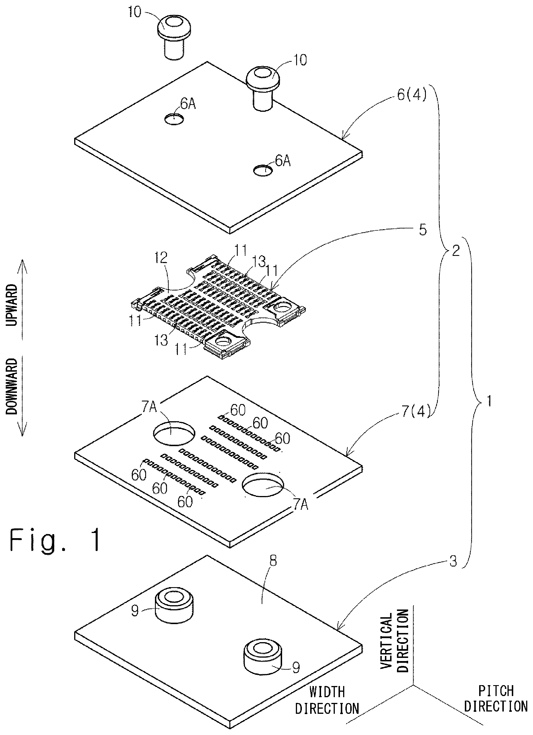
are exploded perspective view of an information processing device 1 . As shown in , the information processing device 1 includes a differential transmission assembly 2 (assembly) and a support board 3 .
The differential transmission assembly 2 includes a differential transmission board set 4 and a compression connector 5 .
The differential transmission board set 4 includes a contact board 6 and a mounting board 7 . The contact board 6 and the mounting board 7 are electrically connected to each other through the compression connector 5 . The contact board 6 and the mounting board 7 are both differential transmission boards. The contact board 6 and the mounting board 7 are parallel to each other in the state of being electrically connected to each other through the compression connector 5 .
The contact board 6 has two bolt fastening holes 6 A. Likewise, the mounting board 7 has two bolt fastening holes 7 A.
The support board 3 is typically a part of a housing that accommodates the contact board 6 , the compression connector 5 , and the mounting board 7 , and it is made of aluminum or an aluminum alloy, for example. The support board 3 includes a flat-plate board main body 8 and two nuts 9 projecting from the board main body 8 .
The information processing device 1 is assembled as follows. First, the compression connector 5 is mounted on the mounting board 7 . Next, the mounting board 7 on which the compression connector 5 is mounted is attached to the support board 3 . At this time, the two nuts 9 of the support board 3 penetrate through the two bolt fastening holes 7 A of the mounting board 7 .
Then, the contact board 6 is attached to the support board 3 in such a way that the contact board 6 overlaps the compression connector 5 . To be specific, two bolts 10 are respectively fastened to the two nuts 9 of the support board 3 through the two bolt fastening holes 6 A of the contact board 6 . The contact board 6 is thereby pressed against the compression connector 5 and comes into contact with the compression connector 5 , and consequently the contact board 6 and the mounting board 7 are electrically connected to each other through the compression connector 5 . Specifically, the compression connector 5 is not mounted on the contact board 6 , and the compression connector 5 and the contact board 6 come into contact with each other only when the contact board 6 is pressed against the compression connector 5 .
Referring still to , the compression connector 5 includes a plurality of compression contacts 11 and a housing 12 that holds the plurality of compression contacts 11 . The plurality of compression contacts 11 form a plurality of contact rows 13 . The plurality of contact rows 13 extend parallel to one another.
A pitch direction, a width direction, and a vertical direction are defined as below. The pitch direction, the width direction, and the vertical direction are orthogonal to each other. The pitch direction is the row direction of each contact row 13 . The width direction is the direction in which the plurality of contact rows 13 extending parallel to one another are arranged. The vertical direction is the direction in which the contact board 6 and the compression connector 5 , and the compression connector 5 and the mounting board 7 are respectively opposed to each other. Thus, the thickness direction of the contact board 6 and the thickness direction of the mounting board 7 correspond to the vertical direction. The direction of viewing the contact board 6 from the compression connector 5 is referred to as upward, and the direction of viewing the mounting board 7 from the compression connector 5 is referred to as downward. The vertical direction is the direction used by way of illustration only and should not be interpreted as limiting the position of the information processing device 1 when actually used.
is a cross-sectional view of the differential transmission assembly 2 . As shown in , each compression contact 11 is accommodated by press fitting into a contact accommodation room 12 A of the housing 12 . Each compression contact 11 includes a soldering part 20 , a spring part 21 , and a press-fit part 22 . The spring part 21 has a contact point part 21 A that is elastically displaceable in the vertical direction. The spring part 21 is supported like a cantilever beam by the press-fit part 22 , and thereby the contact point part 21 A is elastically displaceable in the vertical direction.
The contact board 6 is a multilayer board in which a plurality of conductor layers 6 CL and a plurality of insulator layers 6 SL are laminated alternately. The plurality of conductor layers 6 CL include a first conductor layer 6 CL 1 , a second conductor layer 6 CL 2 , a third conductor layer 6 CL 3 , a fourth conductor layer 6 CL 4 , a fifth conductor layer 6 CL 5 , and a sixth conductor layer 6 CL 6 sequentially from the compression connector 5 side to the upside. The plurality of insulator layers 6 SL include a first insulator layer 6 SL 1 , a second insulator layer 6 SL 2 , a third insulator layer 6 SL 3 , a fourth insulator layer 6 SL 4 , and a fifth insulator layer 6 SL 5 sequentially from the compression connector 5 side to the upside. Thus, the first conductor layer 6 CL 1 , the first insulator layer 6 SL 1 , the second conductor layer 6 CL 2 , the second insulator layer 6 SL 2 , the third conductor layer 6 CL 3 , the third insulator layer 6 SL 3 , the fourth conductor layer 6 CL 4 , the fourth insulator layer 6 SL 4 , the fifth conductor layer 6 CL 5 , the fifth insulator layer 6 SL 5 , and the sixth conductor layer 6 CL 6 are sequentially laminated from the compression connector 5 side to the upside. The laminating direction of the contact board 6 corresponds to the vertical direction. The second conductor layer 6 CL 2 is a conductor layer that is closest to the first conductor layer 6 CL 1 .
Each conductor layer 6 CL is typically made of copper foil with high electrical conductivity. Each insulator layer 6 SL is typically made of glass epoxy.
Likewise, the mounting board 7 is a multilayer board in which a plurality of conductor layers 7 CL and a plurality of insulator layers 7 SL are laminated alternately. The plurality of conductor layers 7 CL include a first conductor layer 7 CL 1 , a second conductor layer 7 CL 2 , a third conductor layer 7 CL 3 , a fourth conductor layer 7 CL 4 , a fifth conductor layer 7 CL 5 , and a sixth conductor layer 7 CL 6 sequentially from the compression connector 5 side to the downside. The plurality of insulator layers 7 SL include a first insulator layer 7 SL 1 , a second insulator layer 7 SL 2 , a third insulator layer 7 SL 3 , a fourth insulator layer 7 SL 4 , and a fifth insulator layer 7 SL 5 sequentially from the compression connector 5 side to the downside. Thus, the first conductor layer 7 CL 1 , the first insulator layer 7 SL 1 , the second conductor layer 7 CL 2 , the second insulator layer 7 SL 2 , the third conductor layer 7 CL 3 , the third insulator layer 7 SL 3 , the fourth conductor layer 7 CL 4 , the fourth insulator layer 7 SL 4 , the fifth conductor layer 7 CL 5 , the fifth insulator layer 7 SL 5 , and the sixth conductor layer 7 CL 6 are sequentially laminated from the compression connector 5 side to the downside. The laminating direction of the mounting board 7 corresponds to the vertical direction. The second conductor layer 7 CL 2 is a conductor layer that is closest to the first conductor layer 7 CL 1 .
Each conductor layer 7 CL is typically made of copper foil with high electrical conductivity. Each insulator layer 7 SL is typically made of glass epoxy.
<Contact Board 6 >
to 9 are partial bottom views of the first conductor layer 6 CL 1 , the second conductor layer 6 CL 2 , the third conductor layer 6 CL 3 , the fourth conductor layer 6 CL 4 , the fifth conductor layer 6 CL 5 , and the sixth conductor layer 6 CL 6 of the contact board 6 . In to 9 , a conductor part is indicated by hatching for the sake of visibility.
First, the first conductor layer 6 CL 1 is described hereinafter with reference to . As shown in , the first conductor layer 6 CL 1 includes a plurality of electrode pads 30 respectively corresponding to the plurality of compression contacts 11 of the compression connector 5 . Specifically, the spring part 21 of the corresponding compression contact 11 is able to come into contact with each electrode pad 30 . The plurality of electrode pads 30 form a plurality of pad rows, just like the plurality of compression contacts 11 .
As shown in , in the plurality of electrode pads 30 belonging to each pad row, two ground pads 31 and two signal pads 32 are arranged alternately in the pitch direction. Specifically, the ground pad 31 , the ground pad 31 , the signal pad 32 , the signal pad 32 , the ground pad 31 , the ground pad 31 , the signal pad 32 , the signal pad 32 and so on are arranged sequentially in this recited order along the pitch direction. In other words, the two signal pads 32 for differential transmission are disposed between the two ground pads 31 . shows only four electrode pads 30 . The four electrode pads 30 shown in include two ground pads 31 and two signal pads 32 disposed between the two ground pads 31 . The two ground pads 31 include a first ground pad 33 and a second ground pad 34 . The two signal pads 32 include a first signal pad 35 and a second signal pad 36 . The first ground pad 33 , the first signal pad 35 , the second signal pad 36 , and the second ground pad 34 are arranged in this recited order along the pitch direction.
The first signal pad 35 includes a spring contact part 35 A and a via connection part 35 B. The spring contact part 35 A and the via connection part 35 B are connected to each other in the width direction and thereby formed integrally. For the purpose of illustration, a boundary 35 C between the spring contact part 35 A and the via connection part 35 B is indicated by a dashed line. The spring contact part 35 A includes a base part 35 D that is substantially square and a tapered part 35 E that extends in a tapered shape from the base part 35 D in the width direction.
Likewise, the second signal pad 36 includes a spring contact part 36 A and a via connection part 36 B. The spring contact part 36 A and the via connection part 36 B are connected to each other in the width direction and thereby formed integrally. For the purpose of illustration, a boundary 36 C between the spring contact part 36 A and the via connection part 36 B is indicated by a dashed line. The spring contact part 36 A includes a base part 36 D that is substantially square and a tapered part 36 E that extends in a tapered shape from the base part 36 D in the width direction.
The first ground pad 33 includes a spring contact part 33 A, a first via connection part 33 B, and a second via connection part 33 C. The first via connection part 33 B, the spring contact part 33 A, and the second via connection part 33 C are disposed in this recited order in the width direction. The spring contact part 33 A, the first via connection part 33 B, and the second via connection part 33 C are formed integrally. For the purpose of illustration, a boundary 33 D between the spring contact part 33 A and the first via connection part 33 B is indicated by a dashed line. Likewise, a boundary 33 E between the spring contact part 33 A and the second via connection part 33 C is indicated by a dashed line. The spring contact part 33 A includes a base part 33 F that is substantially square and a tapered part 33 G that extends in a tapered shape from the base part 33 F in the width direction.
Likewise, the second ground pad 34 includes a spring contact part 34 A, a first via connection part 34 B, and a second via connection part 34 C. The first via connection part 34 B, the spring contact part 34 A, and the second via connection part 34 C are disposed in this recited order in the width direction. The spring contact part 34 A, the first via connection part 34 B, and the second via connection part 34 C are formed integrally. For the purpose of illustration, a boundary 34 D between the spring contact part 34 A and the first via connection part 34 B is indicated by a dashed line. Likewise, a boundary 34 E between the spring contact part 34 A and the second via connection part 34 C is indicated by a dashed line. The spring contact part 34 A includes a base part 34 F that is substantially square and a tapered part 34 G that extends in a tapered shape from the base part 34 F in the width direction.
As shown in , the first signal pad 35 and the second signal pad 36 have the same shape, and the first ground pad 33 and the second ground pad 34 have the same shape. The spring contact part 35 A of the first signal pad 35 , the spring contact part 36 A of the second signal pad 36 , the spring contact part 33 A of the first ground pad 33 , and the spring contact part 34 A of the second ground pad 34 have the same shape, and are aligned in the pitch direction. The via connection part 35 B of the first signal pad 35 , the via connection part 36 B of the second signal pad 36 , the first via connection part 33 B of the first ground pad 33 , and the first via connection part 34 B of the second ground pad 34 have the same shape, and are aligned in the pitch direction.
Referring still to , the first ground pad 33 has an inner region 33 P and an outer region 33 Q. The inner region 33 P is a region closer to the first signal pad 35 relative to a dividing line 33 R that divides the pad area of the first ground pad 33 in half in the pitch direction. The outer region 33 Q is a region farther from the first signal pad 35 relative to the dividing line 33 R. The first ground pad 33 has a symmetrical shape with respect to the dividing line 33 R in the pitch direction. The dividing line 33 R is a straight line that extends along the width direction and divides the pad area of the first ground pad 33 into two equal parts in the pitch direction. An area of the inner region 33 P equals to an area of the outer region 33 Q.
Likewise, the second ground pad 34 has an inner region 34 P and an outer region 34 Q. The inner region 34 P is a region closer to the second signal pad 36 relative to a dividing line 34 R that divides the pad area of the second ground pad 34 in half in the pitch direction. The outer region 34 Q is a region farther from the second signal pad 36 relative to the dividing line 34 R. The second ground pad 34 has a symmetrical shape with respect to the dividing line 34 R in the pitch direction. The dividing line 34 R is a straight line that extends along the width direction and divides the pad area of the second ground pad 34 into two equal parts in the pitch direction. An area of the inner region 34 P equals to an area of the outer region 34 Q.
Referring next to , the sixth conductor layer 6 CL 6 is described hereinafter. As shown in , the sixth conductor layer 6 CL 6 includes a first ground pad 43 , a second ground pad 44 , a first signal pad 45 , and a second signal pad 46 respectively corresponding to the first ground pad 33 , the second ground pad 34 , the first signal pad 35 , and the second signal pad 36 shown in .
The first ground pad 43 includes a first via connection part 43 A and a second via connection part 43 B. Although the first via connection part 43 A and the second via connection part 43 B are separated from each other in the width direction, they may be formed integrally.
The second ground pad 44 includes a first via connection part 44 A and a second via connection part 44 B. Although the first via connection part 44 A and the second via connection part 44 B are separated from each other in the width direction, they may be formed integrally.
The first via connection part 43 A of the first ground pad 43 is electrically connected to the first via connection part 33 B of the first ground pad 33 shown in through a via hole 50 A shown in and the like. Likewise, the second via connection part 43 B of the first ground pad 43 is electrically connected to the second via connection part 33 C of the first ground pad 33 shown in through a via hole 50 B shown in and the like.
The first via connection part 44 A of the second ground pad 44 is electrically connected to the first via connection part 34 B of the second ground pad 34 shown in through a via hole 51 A shown in and the like. Likewise, the second via connection part 44 B of the second ground pad 44 is electrically connected to the second via connection part 34 C of the second ground pad 34 shown in through a via hole 51 B shown in and the like.
The first signal pad 45 is electrically connected to the via connection part of the first signal pad 35 shown in through a via hole 52 shown in and the like.
The second signal pad 46 is electrically connected to the via connection part 36 B of the second signal pad 36 shown in through a via hole 53 shown in and the like.
The second conductor layer 6 CL 2 to the fifth conductor layer 6 CL 5 are described hereinafter with reference to to 8 . The second conductor layer 6 CL 2 to the fifth conductor layer 6 CL 5 are continuous with one another through the via hole 50 A, the via hole 50 B, the via hole 51 A and the via hole 51 B, and each of them functions as a ground layer.
As shown in , the second conductor layer 6 CL 2 has a penetrating hole 55 . The penetrating hole 55 has an inner edge 55 A. In , the via hole 52 and the via hole 53 are disposed inside the inner edge 55 A of the penetrating hole 55 . The via hole 50 A, the via hole 50 B, the via hole 51 A and the via hole 51 B are disposed outside the inner edge 55 A of the penetrating hole 55 . The penetrating hole 55 includes a rectangular part 55 B that is substantially rectangular and two extension parts 55 C that extend from the rectangular part 55 B in the pitch direction. One of the two extension parts 55 C extends to run between the via hole 50 A and the via hole 50 B, and the other one extends to run between the via hole 51 A and the via hole 51 B.
As shown in , the third conductor layer 6 CL 3 has a penetrating hole 56 . The penetrating hole 56 has an inner edge 56 A. In , the via hole 52 and the via hole 53 are disposed inside the inner edge 56 A of the penetrating hole 56 . The via hole 50 A, the via hole 50 B, the via hole 51 A and the via hole 51 B are disposed outside the inner edge 56 A of the penetrating hole 56 . The penetrating hole 56 is substantially rectangular.
As shown in , the fourth conductor layer 6 CL 4 has a penetrating hole 57 . The penetrating hole 57 has an inner edge 57 A. In , the via hole 52 and the via hole 53 are disposed inside the inner edge 57 A of the penetrating hole 57 . The via hole 50 A, the via hole 50 B, the via hole 51 A and the via hole 51 B are disposed outside the inner edge 57 A of the penetrating hole 57 . The penetrating hole 57 is substantially rectangular.
As shown in , the fifth conductor layer 6 CL 5 has two penetrating holes 58 . Each penetrating hole 58 has an inner edge 58 A. In , the via hole 52 and the via hole 53 are respectively disposed inside the inner edges 58 A of the two penetrating holes 58 . The via hole 50 A, the via hole 50 B, the via hole 51 A and the via hole 51 B are disposed outside the inner edges 58 A of the two penetrating holes 58 . Each penetrating hole 58 is substantially circular.
is a projection view that projects the inner edge 55 A of the penetrating hole 55 , the inner edge 56 A of the penetrating hole 56 , and the inner edge 57 A of the penetrating hole 57 on the first conductor layer 6 CL 1 in order to illustrate the positional relationship of the penetrating hole 55 , the penetrating hole 56 and the penetrating hole 57 relative to the first conductor layer 6 CL 1 . The inner edge 55 A of the penetrating hole 55 , the inner edge 56 A of the penetrating hole 56 , and the inner edge 57 A of the penetrating hole 57 are indicated by heavy lines, and the first ground pad 33 , the second ground pad 34 , the first signal pad 35 , and the second signal pad 36 are indicated by alternate long and two short dashes lines. For the purpose of illustration, the outer region 33 Q of the first ground pad 33 and the outer region 34 Q of the second ground pad 34 are indicated by hatching.
As shown in , in the contact board 6 , the penetrating hole 55 is formed in such a way that the first signal pad 35 and the second signal pad 36 are both located inside the inner edge 55 A of the penetrating hole 55 when viewed in the vertical direction. Specifically, the inner edge 55 A of the penetrating hole 55 surrounds the first signal pad 35 and the second signal pad 36 . In other words, the first signal pad 35 and the second signal pad 36 overlap one penetrating hole 55 that is formed in an unbroken manner.
Further, the penetrating hole 55 is formed to overlap the outer region 33 Q of the first ground pad 33 and the outer region 34 Q of the second ground pad 34 when viewed in the vertical direction. Specifically, one extension part 55 C of the penetrating hole 55 extends from the rectangular part 55 B across the dividing line 33 R in the pitch direction so as to overlap the outer region 33 Q of the first ground pad 33 , and the other extension part 55 C extends from the rectangular part 55 B across the dividing line 34 R in the pitch direction so as to overlap the outer region 34 Q of the second ground pad 34 .
To be specific, the rectangular part 55 B of the penetrating hole 55 does not overlap the first via connection part 33 B and the second via connection part 33 C of the first ground pad 33 and the first via connection part 34 B and the second via connection part 34 C of the second ground pad 34 , and is in contact with the first via connection part 33 B and the second via connection part 33 C of the first ground pad 33 and the first via connection part 34 B and the second via connection part 34 C of the second ground pad 34 in the pitch direction.
The two extension parts 55 C of the penetrating hole 55 do not overlap the first via connection part 33 B and the second via connection part 33 C of the first ground pad 33 and the first via connection part 34 B and the second via connection part 34 C of the second ground pad 34 , and is in contact with the first via connection part 33 B and the second via connection part 33 C of the first ground pad 33 and the first via connection part 34 B and the second via connection part 34 C of the second ground pad 34 in the width direction.
Thus, two partition lines 55 D that partition the two extension parts 55 C in the inner edge 55 A of the penetrating hole 55 in the pitch direction are largely separated from the first signal pad 35 and the second signal pad 36 in the pitch direction. This means that the second conductor layer 6 CL 2 is away from the first signal pad 35 and the second signal pad 36 in the pitch direction. This allows controlling a decrease in differential impedance in the first signal pad 35 and the second signal pad 36 .
Referring still to , in the contact board 6 , the penetrating hole 56 and the penetrating hole 57 are formed to completely overlap each other when viewed in the vertical direction. Specifically, the inner edge 56 A of the penetrating hole 56 and the inner edge 57 A of the penetrating hole 57 overlap when viewed in the vertical direction. The penetrating hole 56 is formed in such a way that the first signal pad 35 and the second signal pad 36 are both located inside the inner edge 56 A of the penetrating hole 56 . Specifically, the inner edge 56 A of the penetrating hole 56 surrounds the first signal pad 35 and the second signal pad 36 . In other words, the first signal pad 35 and the second signal pad 36 overlap one penetrating hole 56 that is formed in an unbroken manner. The same applies to the penetrating hole 57 .
<Mounting Board 7 >
to 17 are partial plan views of the first conductor layer 7 CL 1 , the second conductor layer 7 CL 2 , the third conductor layer 7 CL 3 , the fourth conductor layer 7 CL 4 , the fifth conductor layer 7 CL 5 , and the sixth conductor layer 7 CL 6 of the mounting board 7 . In to 17 , a conductor part is indicated by hatching for the sake of visibility.
The first conductor layer 7 CL 1 is described first with reference to . As shown in , the first conductor layer 7 CL 1 includes a plurality of electrode pads 60 respectively corresponding to the plurality of compression contacts 11 of the compression connector 5 . Specifically, the soldering part 20 of the corresponding compression contact 11 is able to be soldered to each electrode pad 60 . The plurality of electrode pads 60 form a plurality of pad rows, just like the plurality of compression contacts 11 .
As shown in , in the plurality of electrode pads 60 belonging to each pad row, two ground pads 61 and two signal pads 62 are arranged alternately in the pitch direction. Specifically, the ground pad 61 , the ground pad 61 , the signal pad 62 , the signal pad 62 , the ground pad 61 , the ground pad 61 , the signal pad 62 , the signal pad 62 and so on are arranged sequentially in this recited order along the pitch direction. In other words, the two signal pads 62 for differential transmission are disposed between the two ground pads 61 . shows only four electrode pads 60 . The four electrode pads 60 shown in include two ground pads 61 and two signal pads 62 disposed between the two ground pads 61 . The two ground pads 61 include a first ground pad 63 and a second ground pad 64 . The two signal pads 62 include a first signal pad 65 and a second signal pad 66 . The first ground pad 63 , the first signal pad 65 , the second signal pad 66 , and the second ground pad 64 are arranged in this recited order along the pitch direction.
The first signal pad 65 is substantially square. The dimension of the first signal pad 65 in the pitch direction is smaller than that of the first signal pad 35 shown in . Likewise, the dimension of the first signal pad 65 in the width direction is smaller than that of the first signal pad 35 shown in .
The second signal pad 66 is substantially square. The dimension of the second signal pad 66 in the pitch direction is smaller than that of the second signal pad 36 shown in . Likewise, the dimension of the second signal pad 66 in the width direction is smaller than that of the second signal pad 36 shown in .
In this manner, the first signal pad 35 and the second signal pad 36 of the contact board 6 are larger than the first signal pad 65 and the second signal pad 66 of the mounting board 7 in order to absorb the displacement of the contact board 6 relative to the compression connector 5 in the pitch direction and the width direction.
Referring again to , the first ground pad 63 and the second ground pad 64 extend in the width direction.
As shown in , the first signal pad 65 and the second signal pad 66 have the same shape, and the first ground pad 63 and the second ground pad 64 have the same shape.
Referring still to , the first ground pad 63 has an inner region 63 P and an outer region 63 Q. The inner region 63 P is a region closer to the first signal pad 65 relative to a dividing line 63 R that divides the pad area of the first ground pad 63 in half in the pitch direction. The outer region 63 Q is a region farther from the first signal pad 65 relative to the dividing line 63 R. The first ground pad 63 has a symmetrical shape with respect to the dividing line 63 R in the pitch direction.
Likewise, the second ground pad 64 has an inner region 64 P and an outer region 64 Q. The inner region 64 P is a region closer to the second signal pad 66 relative to a dividing line 64 R that divides the pad area of the second ground pad 64 in half in the pitch direction. The outer region 64 Q is a region farther from the second signal pad 66 relative to the dividing line 64 R. The second ground pad 64 has a symmetrical shape with respect to the dividing line 64 R in the pitch direction.
Referring next to , the sixth conductor layer 7 CL 6 is described hereinafter. As shown in , the sixth conductor layer 7 CL 6 includes a first ground pad 73 , a second ground pad 74 , a first signal pad 75 , and a second signal pad 76 respectively corresponding to the first ground pad 63 , the second ground pad 64 , the first signal pad 65 , and the second signal pad 66 shown in .
The first ground pad 73 includes a first via connection part 73 A and a second via connection part 73 B. Although the first via connection part 73 A and the second via connection part 73 B are separated from each other in the width direction, they may be formed integrally.
The second ground pad 74 includes a first via connection part 74 A and a second via connection part 74 B. Although the first via connection part 74 A and the second via connection part 74 B are separated from each other in the width direction, they may be formed integrally.
The first via connection part 73 A of the first ground pad 73 is electrically connected to an end 63 A of the first ground pad 63 in the width direction shown in through a via hole 80 A shown in and the like. Likewise, the second via connection part 73 B of the first ground pad 73 is electrically connected to the end 63 A of the first ground pad 63 in the width direction shown in through a via hole 80 B shown in and the like.
The first via connection part 74 A of the second ground pad 74 is electrically connected to an end 64 A of the second ground pad 64 in the width direction shown in through a via hole 81 A shown in and the like. Likewise, the second via connection part 74 B of the second ground pad 74 is electrically connected to the end 64 A of the second ground pad 64 in the width direction shown in through a via hole 81 B shown in and the like.
The first signal pad 75 is electrically connected to the first signal pad 65 shown in through a via hole 82 shown in and the like.
The second signal pad 76 is electrically connected to the second signal pad 66 shown in through a via hole 83 shown in and the like.
The second conductor layer 7 CL 2 to the fifth conductor layer 7 CL 5 are described hereinafter with reference to to 15 . The second conductor layer 7 CL 2 to the fifth conductor layer 7 CL 5 are continuous with one another through the via hole 80 A, the via hole 80 B, the via hole 81 A and the via hole 81 B, and each of them functions as a ground layer.
As shown in , the second conductor layer 7 CL 2 has a penetrating hole 85 . The penetrating hole 85 has an inner edge 85 A. In , the via hole 82 and the via hole 83 are disposed inside the inner edge 85 A of the penetrating hole 85 . The via hole 80 A, the via hole 80 B, the via hole 81 A and the via hole 81 B are disposed outside the inner edge 85 A of the penetrating hole 85 . The penetrating hole 85 is substantially rectangular.
As shown in , the third conductor layer 7 CL 3 has a penetrating hole 86 . The penetrating hole 86 has an inner edge 86 A. In , the via hole 82 and the via hole 83 are disposed inside the inner edge 86 A of the penetrating hole 86 . The via hole 80 A, the via hole 80 B, the via hole 81 A and the via hole 81 B are disposed outside the inner edge 86 A of the penetrating hole 86 . The penetrating hole 86 is substantially rectangular.
As shown in , the fourth conductor layer 7 CL 4 has a penetrating hole 87 . The penetrating hole 87 has an inner edge 87 A. In , the via hole 82 and the via hole 83 are disposed inside the inner edge 87 A of the penetrating hole 87 . The via hole 80 A, the via hole 80 B, the via hole 81 A and the via hole 81 B are disposed outside the inner edge 87 A of the penetrating hole 87 . The penetrating hole 87 is substantially rectangular.
As shown in , the fifth conductor layer 7 CL 5 has two penetrating holes 88 . Each penetrating hole 88 has an inner edge 88 A. In , the via hole 82 and the via hole 83 are respectively disposed inside the inner edges 88 A of the two penetrating holes 88 . The via hole 80 A, the via hole 80 B, the via hole 81 A and the via hole 81 B are disposed outside the inner edges 88 A of the two penetrating holes 88 . Each penetrating hole 88 is substantially circular.
is a projection view that projects the inner edge 85 A of the penetrating hole 85 , the inner edge 86 A of the penetrating hole 86 , and the inner edge 87 A of the penetrating hole 87 on the first conductor layer 7 CL 1 in order to illustrate the positional relationship of the penetrating hole 85 , the penetrating hole 86 and the penetrating hole 87 relative to the first conductor layer 7 CL 1 . The inner edge 85 A of the penetrating hole 85 , the inner edge 86 A of the penetrating hole 86 , and the inner edge 87 A of the penetrating hole 87 are indicated by heavy lines, and the first ground pad 63 , the second ground pad 64 , the first signal pad 65 , and the second signal pad 66 are indicated by alternate long and two short dashes lines.
As shown in , in the mounting board 7 , the penetrating hole 85 is formed in such a way that the first signal pad 65 and the second signal pad 66 are both located inside the inner edge 85 A of the penetrating hole 85 when viewed in the vertical direction. Specifically, the inner edge 85 A of the penetrating hole 85 surrounds the first signal pad 65 and the second signal pad 66 . In other words, the first signal pad 65 and the second signal pad 66 overlap one penetrating hole 85 that is formed in an unbroken manner.
Further, the penetrating hole 85 is separated from the first ground pad 63 and the second ground pad 64 in the pitch direction when viewed in the vertical direction. To be specific, one of two partition lines 85 D that partition the penetrating hole 85 in the pitch direction in the inner edge 85 A of the penetrating hole 85 is located between the first ground pad 63 and the first signal pad 65 in the pitch direction and at equal distances from the first ground pad 63 and the first signal pad 65 , and the other one is located between the second ground pad 64 and the second signal pad 66 in the pitch direction and at equal distances from the second ground pad 64 and the second signal pad 66 .
The dimensions in the pitch direction of the first signal pad 65 and the second signal pad 66 are smaller than those of the first signal pad 35 and the second signal pad 36 shown in , and therefore differential impedance does not significantly decrease due to parasitic capacitance. Thus, this is designed to reduce the opening area of the penetrating hole 85 in the second conductor layer 7 CL 2 and prioritize the electromagnetic shield effect by the second conductor layer 7 CL 2 .
Referring still to , in the mounting board 7 , the penetrating hole 85 , the penetrating hole 86 and the penetrating hole 87 are formed to completely overlap with one another when viewed in the vertical direction. Specifically, the inner edge 85 A of the penetrating hole 85 , the inner edge 86 A of the penetrating hole 86 , and the inner edge 87 A of the penetrating hole 87 overlap when viewed in the vertical direction. Thus, the penetrating hole 86 is formed in such a way that the first signal pad 65 and the second signal pad 66 are both located inside the inner edge 86 A of the penetrating hole 86 . Specifically, the inner edge 86 A of the penetrating hole 86 surrounds the first signal pad 65 and the second signal pad 66 . In other words, the first signal pad 65 and the second signal pad 66 overlap one penetrating hole 86 that is formed in an unbroken manner. The same applies to the penetrating hole 87 .
First Modified Example
A first modified example of the first embodiment is described hereinafter with reference to . In , a conductor part is indicated by hatching for the sake of visibility.
As shown in , in the first modified example, the third conductor layer 6 CL 3 and the fourth conductor layer 6 CL 4 have the same structure as the fifth conductor layer 6 CL 5 shown in . Specifically, as shown in , the third conductor layer 6 CL 3 and the fourth conductor layer 6 CL 4 have two penetrating holes 90 . Each penetrating hole 90 has an inner edge 90 A. The via hole 52 and the via hole 53 are respectively located inside the inner edges 90 A of the two penetrating holes 90 . The via hole 50 A, the via hole 50 B, the via hole 51 A and the via hole 51 B are located outside the inner edges 90 A of the two penetrating holes 90 . Each penetrating hole 90 is substantially circular.
In this manner, the two penetrating holes 90 formed in the third conductor layer 6 CL 3 and the fourth conductor layer 6 CL 4 have the minimum necessary size that does not allow the third conductor layer 6 CL 3 and the fourth conductor layer 6 CL 4 to be continuous with the via hole 52 and the via hole 53 . Thus, the third conductor layer 6 CL 3 and the fourth conductor layer 6 CL 4 overlap the first signal pad 35 and the second signal pad 36 indicated by alternate long and two short dashes lines in when viewed in the vertical direction. This is thereby designed to prioritize the electromagnetic shield effect by the third conductor layer 6 CL 3 and the fourth conductor layer 6 CL 4 .
Likewise, as shown in , in the first modified example, the third conductor layer 7 CL 3 and the fourth conductor layer 7 CL 4 have the same structure as the fifth conductor layer 7 CL 5 shown in . Specifically, as shown in , the third conductor layer 7 CL 3 and the fourth conductor layer 7 CL 4 have two penetrating holes 91 . Each penetrating hole 91 has an inner edge 91 A. The via hole 82 and the via hole 83 are respectively located inside the inner edges 91 A of the two penetrating holes 91 . The via hole 80 A, the via hole 80 B, the via hole 81 A and the via hole 81 B are located outside the inner edges 91 A of the two penetrating holes 91 . Each penetrating hole 91 is substantially circular.
In this manner, the two penetrating holes 91 formed in the third conductor layer 7 CL 3 and the fourth conductor layer 7 CL 4 have the minimum necessary size that does not allow the third conductor layer 7 CL 3 and the fourth conductor layer 7 CL 4 to be continuous with the via hole 82 and the via hole 83 . Thus, the third conductor layer 7 CL 3 and the fourth conductor layer 7 CL 4 overlap the first signal pad 65 and the second signal pad 66 indicated by alternate long and two short dashes lines in when viewed in the vertical direction. This is thereby designed to prioritize the electromagnetic shield effect by the third conductor layer 7 CL 3 and the fourth conductor layer 7 CL 4 .
The above-described first modified example is directly applicable to the first to fourth comparative examples described hereinbelow.
First Comparative Example
A first comparative example of the present disclosure is described hereinafter with reference to . Differences of this comparative example from the above-described first embodiment are mainly described below, and redundant description thereof is omitted.
<Contact Board 6 >
is a projection view that projects the inner edge 55 A of the penetrating hole 55 , the inner edge 56 A of the penetrating hole 56 , and the inner edge 57 A of the penetrating hole 57 on the first conductor layer 6 CL 1 in order to illustrate the positional relationship of the penetrating hole 55 , the penetrating hole 56 and the penetrating hole 57 relative to the first conductor layer 6 CL 1 . The inner edge 55 A of the penetrating hole 55 , the inner edge 56 A of the penetrating hole 56 , and the inner edge 57 A of the penetrating hole 57 are indicated by heavy lines, and the first ground pad 33 , the second ground pad 34 , the first signal pad 35 , and the second signal pad 36 are indicated by alternate long and two short dashes lines. For the purpose of illustration, the outer region 33 Q of the first ground pad 33 and the outer region 34 Q of the second ground pad 34 are indicated by hatching.
As shown in , the contact board 6 in this comparative example has the same structure as the contact board 6 in the above-described first embodiment shown in .
Specifically, as shown in , in the contact board 6 , the penetrating hole 55 is formed in such a way that the first signal pad 35 and the second signal pad 36 are both located inside the inner edge 55 A of the penetrating hole 55 when viewed in the vertical direction. Specifically, the inner edge 55 A of the penetrating hole 55 surrounds the first signal pad 35 and the second signal pad 36 . In other words, the first signal pad 35 and the second signal pad 36 overlap one penetrating hole 55 that is formed in an unbroken manner.
Further, the penetrating hole 55 is formed to overlap the outer region 33 Q of the first ground pad 33 and the outer region 34 Q of the second ground pad 34 when viewed in the vertical direction. Specifically, one extension part 55 C of the penetrating hole 55 extends from the rectangular part 55 B across the dividing line 33 R in the pitch direction so as to overlap the outer region 33 Q of the first ground pad 33 , and the other extension part 55 C extends from the rectangular part 55 B across the dividing line 34 R in the pitch direction so as to overlap the outer region 34 Q of the second ground pad 34 .
Thus, two partition lines 55 D that partition the two extension parts 55 C in the inner edge 55 A of the penetrating hole 55 in the pitch direction are largely separated from the first signal pad 35 and the second signal pad 36 in the pitch direction. This means that the second conductor layer 6 CL 2 is away from the first signal pad 35 and the second signal pad 36 in the pitch direction. This allows controlling a decrease in differential impedance in the first signal pad 35 and the second signal pad 36 .
<Mounting Board 7 >
is a projection view that projects the inner edge 85 A of the penetrating hole 85 , the inner edge 86 A of the penetrating hole 86 , and the inner edge 87 A of the penetrating hole 87 on the first conductor layer 7 CL 1 in order to illustrate the positional relationship of the penetrating hole 85 , the penetrating hole 86 and the penetrating hole 87 relative to the first conductor layer 7 CL 1 . The inner edge 85 A of the penetrating hole 85 , the inner edge 86 A of the penetrating hole 86 , and the inner edge 87 A of the penetrating hole 87 are indicated by heavy lines, and the first ground pad 63 , the second ground pad 64 , the first signal pad 65 , and the second signal pad 66 are indicated by alternate long and two short dashes lines. For the purpose of illustration, the outer region 63 Q of the first ground pad 63 and the outer region 64 Q of the second ground pad 64 are indicated by hatching.
As shown in , this comparative example is different from the above-described first embodiment in the shape of the penetrating hole 85 of the second conductor layer 7 CL 2 , and the other structure is the same as that of the first embodiment. Specifically, the penetrating hole 85 in this comparative example is wider in the pitch direction than the penetrating hole 85 in the first embodiment shown in .
Specifically, as shown in , the penetrating hole 85 includes a rectangular part 85 B that is substantially rectangular and two extension parts 85 C that extend from the rectangular part 85 B in the pitch direction. One of the two extension parts 85 C extends to run between the via hole 80 A and the via hole 80 B, and the other one extends to run between the via hole 81 A and the via hole 81 B.
Further, the penetrating hole 85 is formed to overlap the outer region 63 Q of the first ground pad 63 and the outer region 64 Q of the second ground pad 64 when viewed in the vertical direction. Specifically, one extension part 85 C of the penetrating hole 85 extends from the rectangular part 85 B across the dividing line 63 R in the pitch direction so as to overlap the outer region 63 Q of the first ground pad 63 , and the other extension part 85 C extends from the rectangular part 85 B across the dividing line 64 R in the pitch direction so as to overlap the outer region 64 Q of the second ground pad 64 .
Thus, two partition lines 85 D that partition the two extension parts 85 C in the inner edge 85 A of the penetrating hole 85 in the pitch direction are largely separated from the first signal pad 65 and the second signal pad 66 in the pitch direction. This means that the second conductor layer 7 CL 2 is away from the first signal pad 65 and the second signal pad 66 in the pitch direction. This allows controlling a decrease in differential impedance in the first signal pad 65 and the second signal pad 66 .
Second Comparative Example
A second comparative example of the present disclosure is described hereinafter with reference to . Differences of this comparative example from the above-described first embodiment are mainly described below, and redundant description thereof is omitted.
<Contact Board 6 >
is a projection view that projects the inner edge 55 A of the penetrating hole 55 , the inner edge 56 A of the penetrating hole 56 , and the inner edge 57 A of the penetrating hole 57 on the first conductor layer 6 CL 1 in order to illustrate the positional relationship of the penetrating hole 55 , the penetrating hole 56 and the penetrating hole 57 relative to the first conductor layer 6 CL 1 . The inner edge 55 A of the penetrating hole 55 , the inner edge 56 A of the penetrating hole 56 , and the inner edge 57 A of the penetrating hole 57 are indicated by heavy lines, and the first ground pad 33 , the second ground pad 34 , the first signal pad 35 , and the second signal pad 36 are indicated by alternate long and two short dashes lines. For the purpose of illustration, the outer region 33 Q of the first ground pad 33 and the outer region 34 Q of the second ground pad 34 are indicated by hatching.
As shown in , the contact board 6 in this comparative example has the same structure as the contact board 6 in the above-described first embodiment shown in .
Specifically, as shown in , in the contact board 6 , the penetrating hole 55 is formed in such a way that the first signal pad 35 and the second signal pad 36 are both located inside the inner edge 55 A of the penetrating hole 55 when viewed in the vertical direction. Specifically, the inner edge 55 A of the penetrating hole 55 surrounds the first signal pad 35 and the second signal pad 36 . In other words, the first signal pad 35 and the second signal pad 36 overlap one penetrating hole 55 that is formed in an unbroken manner.
Further, the penetrating hole 55 is formed to overlap the outer region 33 Q of the first ground pad 33 and the outer region 34 Q of the second ground pad 34 when viewed in the vertical direction. Specifically, one extension part 55 C of the penetrating hole 55 extends from the rectangular part 55 B across the dividing line 33 R in the pitch direction so as to overlap the outer region 33 Q of the first ground pad 33 , and the other extension part 55 C extends from the rectangular part 55 B across the dividing line 34 R in the pitch direction so as to overlap the outer region 34 Q of the second ground pad 34 .
Thus, two partition lines 55 D that partition the two extension parts 55 C in the inner edge 55 A of the penetrating hole 55 in the pitch direction are largely separated from the first signal pad 35 and the second signal pad 36 in the pitch direction. This means that the second conductor layer 6 CL 2 is away from the first signal pad 35 and the second signal pad 36 in the pitch direction. This allows controlling a decrease in differential impedance in the first signal pad 35 and the second signal pad 36 .
<Mounting Board 7 >
is a projection view that projects the inner edge 85 A of the penetrating hole 85 , the inner edge 86 A of the penetrating hole 86 , and the inner edge 87 A of the penetrating hole 87 on the first conductor layer 7 CL 1 in order to illustrate the positional relationship of the penetrating hole 85 , the penetrating hole 86 and the penetrating hole 87 relative to the first conductor layer 7 CL 1 . The inner edge 85 A of the penetrating hole 85 , the inner edge 86 A of the penetrating hole 86 , and the inner edge 87 A of the penetrating hole 87 are indicated by heavy lines, and the first ground pad 63 , the second ground pad 64 , the first signal pad 65 , and the second signal pad 66 are indicated by alternate long and two short dashes lines. For the purpose of illustration, the inner region 63 P and the outer region 63 Q of the first ground pad 63 and the inner region 64 P and the outer region 64 Q of the second ground pad 64 are indicated by hatching.
As shown in , this comparative example is different from the above-described first embodiment in the shape of the penetrating hole 85 of the second conductor layer 7 CL 2 , and the other structure is the same as that of the first embodiment. Specifically, the penetrating hole 85 in this comparative example is wider in the pitch direction than the penetrating hole 85 in the first embodiment shown in .
To be specific, as shown in , the penetrating hole 85 is formed not to overlap the outer region 63 Q of the first ground pad 63 and the outer region 64 Q of the second ground pad 64 when viewed in the vertical direction. Further, the penetrating hole 85 is formed not to overlap the inner region 63 P of the first ground pad 63 and the inner region 64 P of the second ground pad 64 when viewed in the vertical direction. However, the penetrating hole 85 extends in the pitch direction to come into contact with the inner region 63 P of the first ground pad 63 and the inner region 64 P of the second ground pad 64 when viewed in the vertical direction.
Specifically, one of two partition lines 85 D that partition the penetrating hole 85 in the pitch direction in the inner edge 85 A of the penetrating hole 85 overlaps an outline 63 S of the first ground pad 63 on the first signal pad 65 side, and the other one overlaps an outline 64 S of the second ground pad 64 on the second signal pad 66 side. In this manner, the second conductor layer 7 CL 2 is away from the first signal pad 65 and the second signal pad 66 in the pitch direction, so that it is designed to control a decrease in differential impedance in the first signal pad 65 and the second signal pad 66 , and reduce the opening area of the penetrating hole 85 in the second conductor layer 7 CL 2 and enhance the electromagnetic shield effect by the second conductor layer 7 CL 2 .
Note that, however, in this comparative example, the penetrating hole 85 may be formed to overlap the inner region 63 P of the first ground pad 63 and the inner region 64 P of the second ground pad 64 as long as it does not overlap the outer region 63 Q of the first ground pad 63 and the outer region 64 Q of the second ground pad 64 when viewed in the vertical direction. Specifically, the penetrating hole 85 may run across the outline 63 S of the first ground pad 63 in the pitch direction and overlap the inner region 63 P, and may run across the outline 64 S of the second ground pad 64 in the pitch direction and overlap the inner region 64 P. In this case also, the effect of controlling a decrease in differential impedance in the first signal pad 65 and the second signal pad 66 and the electromagnetic shield effect by the second conductor layer 7 CL 2 are achieved at the same time.
Third Comparative Example
A third comparative example of the present disclosure is described hereinafter with reference to . Differences of this comparative example from the above-described first embodiment are mainly described below, and redundant description thereof is omitted.
<Contact Board 6 >
is a projection view that projects the inner edge 55 A of the penetrating hole 55 , the inner edge 56 A of the penetrating hole 56 , and the inner edge 57 A of the penetrating hole 57 on the first conductor layer 6 CL 1 in order to illustrate the positional relationship of the penetrating hole 55 , the penetrating hole 56 and the penetrating hole 57 relative to the first conductor layer 6 CL 1 . The inner edge 55 A of the penetrating hole 55 , the inner edge 56 A of the penetrating hole 56 , and the inner edge 57 A of the penetrating hole 57 are indicated by heavy lines, and the first ground pad 33 , the second ground pad 34 , the first signal pad 35 , and the second signal pad 36 are indicated by alternate long and two short dashes lines. For the purpose of illustration, the inner region 33 P and the outer region 33 Q of the first ground pad 33 and the inner region 34 P and the outer region 34 Q of the second ground pad 34 are indicated by hatching.
As shown in , this comparative example is different from the above-described first embodiment in the shape of the penetrating hole 55 of the first conductor layer 6 CL 1 , and the other structure is the same as that of the first embodiment. Specifically, the penetrating hole 55 in this comparative example is narrower in the pitch direction than the penetrating hole 55 in the first embodiment shown in . Further, the penetrating hole 55 in this comparative example is substantially rectangular.
To be specific, as shown in , the penetrating hole 55 is formed so as not to overlap the outer region 33 Q of the first ground pad 33 and the outer region 34 Q of the second ground pad 34 when viewed in the vertical direction. However, the penetrating hole 55 extends in the pitch direction so as to overlap the inner region 33 P of the first ground pad 33 and the inner region 34 P of the second ground pad 34 when viewed in the vertical direction. Specifically, the penetrating hole 55 runs across an outline 33 S of the first ground pad 33 on the first signal pad 35 side in the pitch direction and overlaps the inner region 33 P, and further runs across an outline 34 S of the second ground pad 34 on the second signal pad 36 side in the pitch direction and overlaps the inner region 34 P. In this manner, the second conductor layer 6 CL 2 is away from the first signal pad 35 and the second signal pad 36 in the pitch direction, so that it is designed to control a decrease in differential impedance in the first signal pad 35 and the second signal pad 36 , and reduce the opening area of the penetrating hole 55 in the second conductor layer 6 CL 2 and enhance the electromagnetic shield effect by the second conductor layer 6 CL 2 .
Note that, in this comparative example, one of the two partition lines 55 D that partition the penetrating hole 55 in the pitch direction in the inner edge 55 A of the penetrating hole 55 may overlap the outline 33 S of the first ground pad 33 , and the other one may overlap the outline 34 S of the second ground pad 34 . In other words, the penetrating hole 55 may be formed to come into contact with the inner region 33 P of the first ground pad 33 and the inner region 34 P of the second ground pad 34 when viewed in the vertical direction. In this case also, the effect of controlling a decrease in differential impedance in the first signal pad 35 and the second signal pad 36 and the electromagnetic shield effect by the second conductor layer 6 CL 2 are achieved at the same time.
<Mounting Board 7 >
is a projection view that projects the inner edge 85 A of the penetrating hole 85 , the inner edge 86 A of the penetrating hole 86 , and the inner edge 87 A of the penetrating hole 87 on the first conductor layer 7 CL 1 in order to illustrate the positional relationship of the penetrating hole 85 , the penetrating hole 86 and the penetrating hole 87 relative to the first conductor layer 7 CL 1 . The inner edge 85 A of the penetrating hole 85 , the inner edge 86 A of the penetrating hole 86 , and the inner edge 87 A of the penetrating hole 87 are indicated by heavy lines, and the first ground pad 63 , the second ground pad 64 , the first signal pad 65 , and the second signal pad 66 are indicated by alternate long and two short dashes lines. For the purpose of illustration, the outer region 63 Q of the first ground pad 63 and the outer region 64 Q of the second ground pad 64 are indicated by hatching.
As shown in , this comparative example is different from the above-described first embodiment in the shape of the penetrating hole 85 of the second conductor layer 7 CL 2 , and the other structure is the same as that of the first embodiment. Specifically, the penetrating hole 85 in this comparative example is wider in the pitch direction than the penetrating hole 85 in the first embodiment shown in .
Specifically, as shown in , the penetrating hole 85 includes a rectangular part 85 B that is substantially rectangular and two extension parts 85 C that extend from the rectangular part 85 B in the pitch direction. One of the two extension parts 85 C extends to run between the via hole 80 A and the via hole 80 B, and the other one extends to run between the via hole 81 A and the via hole 81 B.
Further, the penetrating hole 85 is formed to overlap the outer region 63 Q of the first ground pad 63 and the outer region 64 Q of the second ground pad 64 when viewed in the vertical direction. Specifically, one extension part 85 C of the penetrating hole 85 extends from the rectangular part 85 B across the dividing line 63 R in the pitch direction so as to overlap the outer region 63 Q of the first ground pad 63 , and the other extension part 85 C extends from the rectangular part 85 B across the dividing line 64 R in the pitch direction so as to overlap the outer region 64 Q of the second ground pad 64 .
Thus, two partition lines 85 D that partition the two extension parts 85 C in the inner edge 85 A of the penetrating hole 85 in the pitch direction are largely separated from the first signal pad 65 and the second signal pad 66 in the pitch direction. This means that the second conductor layer 7 CL 2 is away from the first signal pad 65 and the second signal pad 66 in the pitch direction. This allows controlling a decrease in differential impedance in the first signal pad 65 and the second signal pad 66 .
Fourth Comparative Example
A fourth comparative example of the present disclosure is described hereinafter with reference to . Differences of this comparative example from the above-described first embodiment are mainly described below, and redundant description thereof is omitted.
<Contact Board 6 >
is a projection view that projects the inner edge 55 A of the penetrating hole 55 , the inner edge 56 A of the penetrating hole 56 , and the inner edge 57 A of the penetrating hole 57 on the first conductor layer 6 CL 1 in order to illustrate the positional relationship of the penetrating hole 55 , the penetrating hole 56 and the penetrating hole 57 relative to the first conductor layer 6 CL 1 . The inner edge 55 A of the penetrating hole 55 , the inner edge 56 A of the penetrating hole 56 , and the inner edge 57 A of the penetrating hole 57 are indicated by heavy lines, and the first ground pad 33 , the second ground pad 34 , the first signal pad 35 , and the second signal pad 36 are indicated by alternate long and two short dashes lines.
As shown in , this comparative example is different from the above-described first embodiment in the shape of the penetrating hole 55 of the first conductor layer 6 CL 1 , and the other structure is the same as that of the first embodiment. Specifically, the penetrating hole 55 in this comparative example is narrower in the pitch direction than the penetrating hole 55 in the first embodiment shown in . Further, the penetrating hole 55 in this comparative example is substantially rectangular.
To be specific, as shown in , the penetrating hole 55 is formed to be separated from the first ground pad 33 and the second ground pad 34 in the pitch direction when viewed in the vertical direction. To be specific, one of the two partition lines 55 D that partition the penetrating hole 55 in the pitch direction is located between the first ground pad 33 and the first signal pad 35 in the pitch direction and at equal distances from the first ground pad 33 and the first signal pad 35 , and the other one is located between the second ground pad 34 and the second signal pad 36 in the pitch direction and at equal distances from the second ground pad 34 and the second signal pad 36 . In this manner, this is designed to reduce the opening area of the penetrating hole 55 in the second conductor layer 6 CL 2 and prioritize the electromagnetic shield effect by the second conductor layer 6 CL 2 .
<Mounting Board 7 >
is a projection view that projects the inner edge 85 A of the penetrating hole 85 , the inner edge 86 A of the penetrating hole 86 , and the inner edge 87 A of the penetrating hole 87 on the first conductor layer 7 CL 1 in order to illustrate the positional relationship of the penetrating hole 85 , the penetrating hole 86 and the penetrating hole 87 relative to the first conductor layer 7 CL 1 . The inner edge 85 A of the penetrating hole 85 , the inner edge 86 A of the penetrating hole 86 , and the inner edge 87 A of the penetrating hole 87 are indicated by heavy lines, and the first ground pad 63 , the second ground pad 64 , the first signal pad 65 , and the second signal pad 66 are indicated by alternate long and two short dashes lines. For the purpose of illustration, the outer region 63 Q of the first ground pad 63 and the outer region 64 Q of the second ground pad 64 are indicated by hatching.
As shown in , this comparative example is different from the above-described first embodiment in the shape of the penetrating hole 85 of the second conductor layer 7 CL 2 , and the other structure is the same as that of the first embodiment. Specifically, the penetrating hole 85 in this comparative example is wider in the pitch direction than the penetrating hole 85 in the first embodiment shown in .
Specifically, as shown in , the penetrating hole 85 includes a rectangular part 85 B that is substantially rectangular and two extension parts 85 C that extend from the rectangular part 85 B in the pitch direction. One of the two extension parts 85 C extends to run between the via hole 80 A and the via hole 80 B, and the other one extends to run between the via hole 81 A and the via hole 81 B.
Further, the penetrating hole 85 is formed to overlap the outer region 63 Q of the first ground pad 63 and the outer region 64 Q of the second ground pad 64 when viewed in the vertical direction. Specifically, one extension part 85 C of the penetrating hole 85 extends from the rectangular part 85 B across the dividing line 63 R in the pitch direction so as to overlap the outer region 63 Q of the first ground pad 63 , and the other extension part 85 C extends from the rectangular part 85 B across the dividing line 64 R in the pitch direction so as to overlap the outer region 64 Q of the second ground pad 64 .
Thus, two partition lines 85 D that partition the two extension parts 85 C in the inner edge 85 A of the penetrating hole 85 in the pitch direction are largely separated from the first signal pad 65 and the second signal pad 66 in the pitch direction. This means that the second conductor layer 7 CL 2 is away from the first signal pad 65 and the second signal pad 66 in the pitch direction. This allows controlling a decrease in differential impedance in the first signal pad 65 and the second signal pad 66 .
Fifth Comparative Example
A fifth comparative example of the present disclosure is described hereinafter with reference to . Differences of this comparative example from the above-described first embodiment are mainly described below, and redundant description thereof is omitted.
is a partial bottom view of the second conductor layer 6 CL 2 , the third conductor layer 6 CL 3 , and the fourth conductor layer 6 CL 4 of the contact board 6 in this comparative example. is a partial bottom view of the second conductor layer 7 CL 2 , the third conductor layer 7 CL 3 , and the fourth conductor layer 7 CL 4 of the mounting board 7 in this comparative example. In to 29 , a conductor part is indicated by hatching for the sake of visibility.
This comparative example is different from the above-described first embodiment in the shape of the second conductor layer 6 CL 2 , the third conductor layer 6 CL 3 and the fourth conductor layer 6 CL 4 of the contact board 6 and the second conductor layer 7 CL 2 , the third conductor layer 7 CL 3 and the fourth conductor layer 7 CL 4 of the mounting board 7 , and the other structure is the same as that of the first embodiment.
<Contact Board 6 >
As shown in , the second conductor layer 6 CL 2 has two penetrating holes 100 in place of the penetrating hole 55 shown in . Each penetrating hole 100 has an inner edge 100 A. In , the via hole 52 and the via hole 53 are respectively disposed inside the inner edges 100 A of the two penetrating holes 100 . The via hole 50 A, the via hole 50 B, the via hole 51 A and the via hole 51 B are disposed outside the inner edges 100 A of the two penetrating holes 100 . Each penetrating hole 100 is substantially circular. The third conductor layer 6 CL 3 and the fourth conductor layer 6 CL 4 have the same shape as the second conductor layer 6 CL 2 .
<Mounting Board 7 >
As shown in , the second conductor layer 7 CL 2 has two penetrating holes 101 in place of the penetrating hole 85 shown in . Each penetrating hole 101 has an inner edge 101 A. In , the via hole 82 and the via hole 83 are respectively disposed inside the inner edges 101 A of the two penetrating holes 101 . The via hole 80 A, the via hole 80 B, the via hole 81 A and the via hole 81 B are disposed outside the inner edges 101 A of the two penetrating holes 101 . Each penetrating hole 101 is substantially circular. The third conductor layer 7 CL 3 and the fourth conductor layer 7 CL 4 have the same shape as the second conductor layer 7 CL 2 .
(First Transmission Signal Integrity Analysis)
The transmission signal integrity in the differential transmission board set 4 according to the above-described first embodiment and first to fourth comparative examples was analyzed, and the analysis results are described hereinafter with reference to to 32 .
Ansys HFSS (registered trademark) manufactured by ANSYS, Inc. was used as analysis software. The thickness of each of the plurality of conductor layers 6 CL and the plurality of conductor layers 7 CL was 18 micrometers, the thickness of each of the first insulator layer 6 SL 1 , the fifth insulator layer 6 SL 5 , the first insulator layer 7 SL 1 and the fifth insulator layer 7 SL 5 was 100 micrometers, and the thickness of each of the second insulator layer 6 SL 2 , the third insulator layer 6 SL 3 , the fourth insulator layer 6 SL 4 , the second insulator layer 7 SL 2 , the third insulator layer 7 SL 3 , and the fourth insulator layer 7 SL 4 was 200 micrometers. The pitch of the plurality of compression contacts 11 was 0.7 millimeters. Further, in , the first conductor layer 6 CL 1 and the first conductor layer 7 CL 1 were separated by 0.7 millimeters in the vertical direction. Each of the via hole 50 A, the via hole 50 B, the via hole 51 A and the via hole 51 B of the contact board 6 shown in to 8 had a diameter of 0.12 millimeters. Each of the via hole 80 A, the via hole 80 B, the via hole 81 A and the via hole 81 B of the mounting board 7 shown in to 15 had a diameter of 0.15 millimeters. The dielectric constant of the insulator layer 6 SL and the insulator layer 7 SL was 3.5.
is a graph showing analysis results of the insertion loss of differential transmission using the differential transmission board set 4 . In the graph of , the horizontal axis indicates the frequency, and the vertical axis indicates the insertion loss. In , approximate curves A to E correspond to the first embodiment and the first to fourth comparative examples, respectively.
is a graph showing analysis results of the return loss of differential transmission using the differential transmission board set 4 . In the graph of , the horizontal axis indicates the frequency, and the vertical axis indicates the return loss. In , approximate curves A to E correspond to the first embodiment and the first to fourth comparative examples, respectively.
is a graph showing analysis results of TDR (Time Domain Reflectometry) of differential transmission using the differential transmission board set 4 . In the graph of , the horizontal axis indicates time, and the vertical axis indicates the differential impedance. In , approximate curves A to E correspond to the first embodiment and the first to fourth comparative examples, respectively. As shown in , in the TDR analysis, the differential transmission board set 4 is designed to have a differential impedance of 8552, for example. In , a differential impedance at 0.065 nsec in the horizontal axis indicates a differential impedance in the first signal pad 35 and the second signal pad 36 of the contact board 6 , and a differential impedance at 0.095 nsec in the horizontal axis indicates a differential impedance in the first signal pad and the second signal pad 66 of the mounting board 7 .
shows that excellent transmission characteristics are obtained in the differential transmission board set 4 according to the first embodiment and the first to fourth comparative examples. Particularly, in the first embodiment and the first to third comparative examples, the insertion loss is significantly lower than that in the fourth comparative example.
shows that excellent transmission characteristics are obtained in the differential transmission board set 4 according to the first embodiment and the first to fourth comparative examples. Particularly, in the first embodiment and the first to third comparative examples, the return loss is significantly lower than that in the fourth comparative example. Further, in the first embodiment, the return loss is significantly lower than that in the first to fourth comparative examples.
shows that the differential impedance in the differential transmission board set 4 according to the first embodiment and the first to fourth comparative examples is within a narrow range of +/−1351 of 8552, which is a design value.
In , referring to the differential impedance at 0.065 nsec in the horizontal axis, which is the differential impedance in the first signal pad 35 and the second signal pad 36 of the contact board 6 , a decrease in differential impedance is controlled in the first embodiment and the first to third comparative examples compared with the fourth comparative example. This is possibly because the second conductor layer 6 CL 2 , which is the inner edge 55 A of the penetrating hole 55 , is sufficiently away from the first signal pad 35 and the second signal pad 36 of the contact board 6 in the pitch direction in the first embodiment and the first to third comparative examples as shown in , for example. The result that the insertion loss in the first embodiment and the first to third comparative examples is lower than the insertion loss in the fourth comparative example in is possibly because a decrease in the differential impedance in the first signal pad 35 and the second signal pad 36 of the contact board 6 was effectively controlled. Likewise, the result that the return loss in the first embodiment and the first to third comparative examples is lower than the return loss in the fourth comparative example in is possibly because a decrease in the differential impedance in the first signal pad 35 and the second signal pad 36 of the contact board 6 was effectively controlled.
shows that, referring to the differential impedance at 0.095 nsec in the horizontal axis, which is the differential impedance in the first signal pad 65 and the second signal pad 66 of the mounting board 7 , the differential impedance is further reduced in the first embodiment compared with the first to fourth comparative examples. This is possibly because the second conductor layer 7 CL 2 , which is the penetrating hole 85 , is narrow in the pitch direction in the first embodiment as shown in . However, a decrease in the differential impedance in the first signal pad 65 and the second signal pad 66 of the mounting board 7 does not cause any significant problem. This is because the amount of decrease in differential impedance in the first signal pad 65 and the second signal pad 66 of the mounting board 7 is about one-fifth of that in the first signal pad 35 and the second signal pad 36 of the contact board 6 .
In , referring to the differential impedance at 0.08 nsec in the horizontal axis, which is the differential impedance in the compression contact 11 , the amount of increase in differential impedance is reduced in the first embodiment compared with the first to fourth comparative examples. This is possibly because the differential impedance at 0.095 nsec in the horizontal axis, which is the differential impedance in the first signal pad 65 and the second signal pad 66 of the mounting board 7 , is further reduced in the first embodiment compared with the first to fourth comparative examples as described above. Then, as shown in , the result that the return loss in the first embodiment is particularly lower than that in the first to fourth comparative examples is possibly because the amount of increase in differential impedance in the compression contact 11 is reduced in the first embodiment as shown in . Specifically, in the first embodiment, the return loss is reduced by intentionally diminishing the effect of reducing the amount of decrease in differential impedance in the first signal pad 65 and the second signal pad 66 of the mounting board 7 .
(Second Transmission Signal Integrity Analysis)
The transmission signal integrity in the differential transmission board set 4 in examples where the first modified example is applied to the first embodiment and first to fourth comparative examples and the differential transmission board set 4 in the fifth comparative example was analyzed, and the analysis results are described hereinafter with reference to to 35 . Note that an example where the first modified example is applied to the first embodiment is the first modified example.
Ansys HFSS (registered trademark) manufactured by ANSYS, Inc. was used as analysis software. The thickness of each of the plurality of conductor layers 6 CL and the plurality of conductor layers 7 CL was 18 micrometers, the thickness of each of the first insulator layer 6 SL 1 , the fifth insulator layer 6 SL 5 , the first insulator layer 7 SL 1 and the fifth insulator layer 7 SL 5 was 100 micrometers, and the thickness of each of the second insulator layer 6 SL 2 , the third insulator layer 6 SL 3 , the fourth insulator layer 6 SL 4 , the second insulator layer 7 SL 2 , the third insulator layer 7 SL 3 , and the fourth insulator layer 7 SL 4 was 200 micrometers. The pitch of the plurality of compression contacts 11 was 0.7 millimeters. Further, in , the first conductor layer 6 CL 1 and the first conductor layer 7 CL 1 were separated by 0.7 millimeters in the vertical direction. Each of the via hole 50 A, the via hole 50 B, the via hole 51 A and the via hole 51 B of the contact board 6 shown in to 8 had a diameter of 0.12 millimeters. Each of the via hole 80 A, the via hole 80 B, the via hole 81 A and the via hole 81 B of the mounting board 7 shown in to 15 had a diameter of 0.15 millimeters. The dielectric constant of the insulator layer 6 SL and the insulator layer 7 SL was 3.5.
is a graph showing analysis results of the insertion loss of differential transmission using the differential transmission board set 4 . In the graph of , the horizontal axis indicates the frequency, and the vertical axis indicates the insertion loss. In , an approximate curve A corresponds to the first embodiment, approximate curves A′ to E′ correspond to examples where the first modified example is applied to the first embodiment and first to fourth comparative examples, respectively, and an approximate curve F corresponds to the fifth comparative example.
is a graph showing analysis results of the return loss of differential transmission using the differential transmission board set 4 . In the graph of , the horizontal axis indicates the frequency, and the vertical axis indicates the return loss. In , an approximate curve A corresponds to the first embodiment, approximate curves A′ to E′ correspond to examples where the first modified example is applied to the first embodiment and first to fourth comparative examples, respectively, and an approximate curve F corresponds to the fifth comparative example.
is a graph showing analysis results of TDR (Time Domain Reflectometry) of differential transmission using the differential transmission board set 4 . In the graph of , the horizontal axis indicates time, and the vertical axis indicates the differential impedance. In , an approximate curve A corresponds to the first embodiment, approximate curves A′ to E′ correspond to examples where the first modified example is applied to the first embodiment and first to fourth comparative examples, respectively, and an approximate curve F corresponds to the fifth comparative example. As shown in , in the TDR analysis, the differential transmission board set 4 is designed to have a differential impedance of 8552, for example. In , a differential impedance at 0.065 nsec in the horizontal axis indicates a differential impedance in the first signal pad 35 and the second signal pad 36 of the contact board 6 , and a differential impedance at 0.095 nsec in the horizontal axis indicates a differential impedance in the first signal pad 65 and the second signal pad 66 of the mounting board 7 .
shows that, when the first modified example is applied to the first embodiment and first to fourth comparative examples, although the insertion loss slightly increases, it is still significantly lower than the insertion loss in the fifth comparative example.
shows that, when the first modified example is applied to the first embodiment and first to fourth comparative examples, although the return loss slightly increases, it is still significantly lower than the return loss in the fifth comparative example.
shows that, when the first modified example is applied to the first embodiment and first to fourth comparative examples, although the amount of decrease in differential impedance in the first signal pad 35 and the second signal pad 36 of the contact board 6 slightly increases, it is still significantly smaller than the amount of decrease in the fifth comparative example.
The first embodiment of the present discloser is described above.
The first embodiment described above has the following features.
Specifically, as shown in to 3 , the differential transmission board set 4 includes the mounting board 7 on which the compression connector 5 is mounted and the contact board 6 configured to come into contact with the compression connector 5 . The contact board 6 and the mounting board 7 are electrically connected to each other through the compression connector 5 . The compression connector 5 includes the four compression contacts 11 arranged in a row, each including the soldering part 20 and the spring part 21 , and the housing 12 that holds the four compression contacts 11 . As shown in , the mounting board 7 is a multilayer board in which the plurality of conductor layers 7 CL and the plurality of insulator layers 7 SL are laminated alternately. The contact board 6 is a multilayer board in which the plurality of conductor layers 6 CL and the plurality of insulator layers 6 SL are laminated alternately.
In the mounting board 7 , the plurality of conductor layers 7 CL include the first conductor layer 7 CL 1 and the second conductor layer 7 CL 2 in this recited order from the compression connector 5 side. In the contact board 6 , the plurality of conductor layers 6 CL include the first conductor layer 6 CL 1 and the second conductor layer 6 CL 2 in this recited order from the compression connector 5 side.
As shown in , in the mounting board 7 , the first conductor layer 7 CL 1 includes the four electrode pads 60 corresponding to the four compression contacts 11 . The four electrode pads 60 include the first signal pad 65 , the second signal pad 66 , the first ground pad 63 and the second ground pad 64 . The first ground pad 63 , the first signal pad 65 , the second signal pad 66 and the second ground pad 64 are arranged in this recited order in the pitch direction (first direction). The soldering parts 20 of the four compression contacts 11 are able to be soldered to the first ground pad 63 , the first signal pad 65 , the second signal pad 66 and the second ground pad 64 , respectively.
As shown in , in the contact board 6 , the first conductor layer 6 CL 1 includes the four electrode pads 30 corresponding to the four compression contacts 11 . The four electrode pads 30 include the first signal pad 35 , the second signal pad 36 , the first ground pad 33 and the second ground pad 34 . The first ground pad 33 , the first signal pad 35 , the second signal pad 36 and the second ground pad 34 are arranged in this recited order in the pitch direction (first direction). The spring parts 21 of the four compression contacts 11 are able to come into contact with the first ground pad 33 , the first signal pad 35 , the second signal pad 36 and the second ground pad 34 , respectively.
As shown in , in the mounting board 7 , the second conductor layer 7 CL 2 is a ground layer and has the penetrating hole 85 . As shown in , in the mounting board 7 , the penetrating hole 85 is formed in such a way that the first signal pad 65 and the second signal pad 66 are both located inside the inner edge of the penetrating hole 85 when viewed in the vertical direction (in the laminating direction). As shown in , in the mounting board 7 , the first ground pad 63 includes the inner region 63 P that is closer to the first signal pad 65 relative to the dividing line 63 R that divides the pad area of the first ground pad 63 in half in the pitch direction, and the outer region 63 Q that is farther from the first signal pad 65 relative to the dividing line 63 R. In the mounting board 7 , the second ground pad 64 includes the inner region 64 P that is closer to the second signal pad 66 relative to the dividing line 64 R that divides the pad area of the second ground pad 64 in half in the pitch direction, and the outer region 64 Q that is farther from the second signal pad 66 relative to the dividing line 64 R.
As shown in , in the contact board 6 , the second conductor layer 6 CL 2 is a ground layer and has the penetrating hole 55 . As shown in , in the contact board 6 , the penetrating hole 55 is formed in such a way that the first signal pad 35 and the second signal pad 36 are both located inside the inner edge of the penetrating hole 55 when viewed in the vertical direction (in the laminating direction). As shown in , in the contact board 6 , the first ground pad 33 includes the inner region 33 P that is closer to the first signal pad 35 relative to the dividing line 33 R that divides the pad area of the first ground pad 33 in half in the pitch direction, and the outer region 33 Q that is farther from the first signal pad 35 relative to the dividing line 33 R. In the contact board 6 , the second ground pad 34 includes the inner region 34 P that is closer to the second signal pad 36 relative to the dividing line 34 R that divides the pad area of the second ground pad 34 in half in the pitch direction, and the outer region 34 Q that is farther from the second signal pad 36 relative to the dividing line 34 R.
As shown in of the first embodiment, in the contact board 6 , the penetrating hole 55 is formed to overlap the outer region 33 Q of the first ground pad 33 and the outer region 34 Q of the second ground pad 34 when viewed in the vertical direction. On the other hand, as shown in of the first embodiment, in the mounting board 7 , the penetrating hole 85 is formed to be away from the first ground pad 63 and the second ground pad 64 when viewed in the vertical direction.
In this structure, as shown in , the differential transmission board set 4 having excellent transmission characteristics is achieved. Particularly, excellent transmission characteristics are achieved compared with the first to fourth comparative examples indicated by the approximate curves B, C, D and E.
The first modified example described above has the following feature.
As shown in , in the mounting board 7 , the third conductor layer 7 CL 3 is a ground layer and overlaps the first signal pad 65 and the second signal pad 66 in the vertical direction. Further, as shown in , in the contact board 6 , the third conductor layer 6 CL 3 is a ground layer and overlaps the first signal pad 35 and the second signal pad 36 in the vertical direction.
In this structure also, as shown in , the differential transmission board set 4 having excellent transmission characteristics is achieved. Further, the electromagnetic shield effect in the third conductor layer 7 CL 3 and the third conductor layer 6 CL 3 is expected to be achieved.
The first embodiment described above has the following features.
Specifically, as shown in , in the mounting board 7 , the third conductor layer 7 CL 3 and the fourth conductor layer 7 CL 4 are ground layers and have the penetrating hole 86 and the penetrating hole 87 , respectively. As shown in , in the mounting board 7 , the penetrating hole 86 of the third conductor layer 7 CL 3 is formed in such a way that the first signal pad 65 and the second signal pad 66 are both located inside the inner edge 86 A of the penetrating hole 86 when viewed in the vertical direction. Likewise, the penetrating hole 87 of the fourth conductor layer 7 CL 4 is formed in such a way that the first signal pad 65 and the second signal pad 66 are both located inside the inner edge 87 A of the penetrating hole 87 when viewed in the vertical direction. As shown in , in the mounting board 7 , the fifth conductor layer 7 CL 5 is a ground layer and overlaps the first signal pad 65 and the second signal pad 66 in the vertical direction (see for better understanding).
Further, as shown in , in the contact board 6 , the third conductor layer 6 CL 3 and the fourth conductor layer 6 CL 4 are ground layers and have the penetrating hole 56 and the penetrating hole 57 , respectively. As shown in , in the contact board 6 , the penetrating hole 56 of the third conductor layer 6 CL 3 is formed in such a way that the first signal pad 35 and the second signal pad 36 are both located inside the inner edge 56 A of the penetrating hole 56 when viewed in the vertical direction. Likewise, the penetrating hole 57 of the fourth conductor layer 6 CL 4 is formed in such a way that the first signal pad 35 and the second signal pad 36 are both located inside the inner edge 57 A of the penetrating hole 57 when viewed in the vertical direction. As shown in , in the contact board 6 , the fifth conductor layer 6 CL 5 is a ground layer and overlaps the first signal pad 35 and the second signal pad 36 in the vertical direction (see for better understanding).
In this structure, as shown in , the differential transmission board set 4 having excellent transmission characteristics is achieved.
Further, as shown in , the compression connector 5 includes a plurality of compression contact groups 11 G, each including the four compression contacts 11 arranged in a row.
Further, the plurality of conductor layers 6 CL of the contact board 6 include the first conductor layer 6 CL 1 , the second conductor layer 6 CL 2 , . . . , the (N−1)th conductor layer, and the Nth conductor layer in this recited order from the compression connector 5 side. N is a natural number of 4 or more. In the first embodiment, the (N−1)th conductor layer and the Nth conductor layer correspond to the fifth conductor layer 6 CL 5 and the sixth conductor layer 6 CL 6 , respectively. The sixth conductor layer 6 CL 6 (the Nth conductor layer) includes the first signal pad 45 and the second signal pad 46 that are electrically connected to the first signal pad 35 and the second signal pad 36 of the first conductor layer 6 CL 1 , respectively. As shown in , the fifth conductor layer 6 CL 5 (the (N−1)th conductor layer) is a ground layer and overlaps the first signal pad 45 and the second signal pad 46 of the sixth conductor layer 6 CL 6 in the laminating direction. In this structure, the electromagnetic shield effect of the first signal pad 45 and the second signal pad 46 of the sixth conductor layer 6 CL 6 (the Nth conductor layer) is sufficiently large.
Likewise, the plurality of conductor layers 7 CL of the mounting board 7 include the first conductor layer 7 CL 1 , the second conductor layer 7 CL 2 , . . . , the (N−1)th conductor layer, and the Nth conductor layer in this recited order from the compression connector 5 side. N is a natural number of 4 or more. In the first embodiment, the (N−1)th conductor layer and the Nth conductor layer correspond to the fifth conductor layer 7 CL 5 and the sixth conductor layer 7 CL 6 , respectively. The sixth conductor layer 7 CL 6 (the Nth conductor layer) includes the first signal pad 75 and the second signal pad 76 that are electrically connected to the first signal pad 65 and the second signal pad 66 of the first conductor layer 7 CL 1 , respectively. As shown in , the fifth conductor layer 7 CL 5 (the (N−1)th conductor layer) is a ground layer and overlaps the first signal pad 75 and the second signal pad 76 of the sixth conductor layer 7 CL 6 in the laminating direction. In this structure, the electromagnetic shield effect of the first signal pad 75 and the second signal pad 76 of the sixth conductor layer 7 CL 6 (the Nth conductor layer) is sufficiently large.
Note that both of the contact board 6 and the mounting board 7 may have the feature of the (N−1)th conductor layer described above, and only one of the contact board 6 and the mounting board 7 may have the feature of the (N−1)th conductor layer described above.
The above-described first embodiment may be modified as follows, for example.
Specifically, in , any one of the via hole 50 A and the via hole 50 B may be omitted. In , any one of the via hole 51 A and the via hole 51 B may be omitted. In , any one of the via hole 80 A and the via hole 80 B may be omitted. In , any one of the via hole 81 A and the via hole 81 B may be omitted.
Further, as shown in , in the first embodiment, the contact board 6 includes the first to sixth conductor layers as the plurality of conductor layers 6 CL. Alternatively, the contact board 6 may further include the seventh and eighth conductor layers as the plurality of conductor layers 6 CL. The sixth conductor layer 6 CL 6 , the seventh conductor layer and the eighth conductor layer are arranged sequentially from the compression connector 5 side. In this case, the seventh and eighth conductor layers are typically ground layers. The seventh and eighth conductor layers may have any thickness and shape. The same applies to the mounting board 7 .
From the disclosure thus described, it will be obvious that the embodiments of the disclosure may be varied in many ways. Such variations are not to be regarded as a departure from the spirit and scope of the disclosure, and all such modifications as would be obvious to one skilled in the art are intended for inclusion within the scope of the following claims.
Figures (20)
Citations
This patent cites (11)
- US7056128
- US7737367
- US2017/0303395
- US2021/0305734
- US2021/0384658
- US2022/0181775
- US2023/0402775
- US2017027721
- US2021157993
- US20170048575
- US20210099165