Differential-follower Control Circuit
Abstract
A differential-follower control circuit has been provided, comprising: a follower; an output-voltage following module, which controls a voltage at a control terminal of the follower to vary with an output voltage; a substrate-voltage following module, which controls a substrate voltage of an output transistor of the follower to vary with an input voltage; an output terminal of the follower is connected to a first terminal of the output-voltage following module; a second terminal of the output-voltage following module is connected to the control terminal of the follower; a first terminal of the substrate-voltage following module is connected to an input terminal of the follower and a second terminal of the substrate-voltage following module is connected to a substrate of the output transistor; the invention effectively improves the overall linearity of the follower.
Claims (9)
1. A differential-follower control circuit, comprising: a follower; an output-voltage following module, which controls a voltage at a control terminal of the follower to vary with an output voltage; and a substrate-voltage following module, which controls a substrate voltage of an output transistor of the follower to vary with an input voltage; wherein an output terminal of the follower is connected to a first terminal of the output-voltage following module, and a second terminal of the output-voltage following module is connected to the control terminal of the follower; a first terminal of the substrate-voltage following module is connected to an input terminal of the follower and a second terminal of the substrate-voltage following module is connected to a substrate of the output transistor.
Show 8 dependent claims
2. The differential-follower control circuit according to claim 1 , wherein the follower comprises a first MOS transistor, a second MOS transistor, and a first constant current source; wherein the first MOS transistor is the output transistor of the follower, a source of the first MOS transistor outputs the output voltage, the source of the first MOS transistor is also connected to one terminal of the first constant current source, a gate of the first MOS transistor is connected to the input voltage, a drain of the first MOS transistor is connected to a source of the second MOS transistor, and a substrate of the first MOS transistor is connected to the substrate-voltage following module; wherein a gate of the second MOS transistor is the control terminal of the follower, and a drain of the second MOS transistor is connected to a supply voltage.
3. The differential-follower control circuit according to claim 1 , wherein the output-voltage following module comprises a second constant current source, and a voltage following unit for detecting and tracking changes in the output voltage of the output transistor, wherein one terminal of the voltage following unit is connected to a source of the output transistor and the other terminal of the voltage following unit is connected to a negative terminal of the second constant current source and the control terminal of the follower, respectively; wherein a positive terminal of the second constant current source is connected to a supply voltage.
4. The differential-follower control circuit according to claim 3 , wherein the voltage following unit comprises at least one resistor and one compensation capacitor, and the at least one resistor and the compensation capacitor are connected in parallel.
5. The differential-follower control circuit according to claim 1 , wherein the substrate-voltage following module comprises a third constant current source and a third MOS transistor, wherein a positive terminal of the third constant current source is connected to the supply voltage, and a negative terminal of the third constant current source is connected to a source of the third MOS transistor; wherein a gate of the third MOS transistor is connected to an input of the output transistor, and a drain of the third MOS transistor is grounded; wherein the source of the third MOS transistor is connected to a substrate of the first MOS transistor.
6. The differential-follower control circuit according to claim 2 , wherein the first MOS transistor and the second MOS transistor are both NMOS transistors.
7. The differential-follower control circuit according to claim 5 , wherein the third MOS transistor is a PMOS transistor.
8. The differential-follower control circuit according to claim 1 , further comprising a sampling network, wherein the sampling network is connected to an output voltage of the output transistor and uses the output voltage as a driving voltage to drive the sampling network for voltage sampling.
9. The differential-follower control circuit according to claim 8 , wherein the sampling network comprises a sampling capacitor, wherein one terminal of the sampling capacitor is connected to a source of the output transistor and the other terminal of the sampling capacitor is grounded.
Full Description
Show full text →
FIELD OF TECHNOLOGY
The present disclosure generally relates to the field of integrated circuit design, and in particular to a differential-follower control circuit.
BACKGROUND
In recent years, with the continuous advancement of integrated circuit manufacturing techniques, the characteristic size of MOS transistors has been continuously reduced, and the operating voltage of the corresponding integrated circuit has also been continuously reduced, resulting in a significant reduction in power consumption and further increase in speed of the integrated circuit. However, the output impedance of MOS transistors is also decreasing, and due to the reduction of operating voltage, it has been difficult to use multiple MOS transistors connected in series to achieve a high output impedance, because such structure will consume a large voltage margin.
The above problem poses a challenge for high output impedance applications. Due to the increasing speed of analog-to-digital converters, a follower must be added to the sampling front-end of an analog-to-digital converter, when designing the circuit. The purpose of this follower is to isolate a sampling network inside the chip from the circuit on the board, while driving the sampling network inside the chip. However, when the substrate of a traditional source follower is grounded, a substrate bias effect will occur, and there will be an increased parasitic capacitance when the substrate and the source of the follower are connected, both of which will have a large impact on the linearity of the follower.
SUMMARY
The present disclosure proposes a differential-follower control circuit.
The technical solution used in the present disclosure is as follows.
A differential-follower control circuit, comprising:
•
• a follower; • an output-voltage following module, which controls a voltage at a control terminal of the follower to vary with an output voltage; and • a substrate-voltage following module, which controls a substrate voltage of an output transistor of the follower to vary with an input voltage; • wherein an output terminal of the follower is connected to a first terminal of the output-voltage following module, a second terminal of the output-voltage following module is connected to the control terminal of the follower; a first terminal of the substrate-voltage following module is connected to an input terminal of the follower and a second terminal of the substrate-voltage following module is connected to a substrate of the output transistor.
Optionally, the follower comprises a first MOS transistor, a second MOS transistor, and a first constant current source; wherein the first MOS transistor is the output transistor of the follower, a source of the first MOS transistor outputs the output voltage, the source of the first MOS transistor is also connected to one terminal of the first constant current source, a gate of the first MOS transistor is connected to the input voltage, a drain of the first MOS transistor is connected to a source of the second MOS transistor, a substrate of the first MOS transistor is connected to the substrate-voltage following module; wherein a gate of the second MOS transistor is the control terminal of the follower, and a drain of the second MOS transistor is connected to a supply voltage.
Optionally, the output-voltage following module comprises a second constant current source, and a voltage following unit for detecting and tracking changes in the output voltage of the output transistor, wherein one terminal of the voltage following unit is connected to a source of the output transistor and the other terminal of the voltage following unit is connected to a negative terminal of the second constant current source and the control terminal of the follower, respectively; wherein a positive terminal of the second constant current source is connected to a supply voltage.
Optionally, the voltage following unit comprises at least one resistor and one compensation capacitor, and the resistor and compensation capacitor are connected in parallel.
Optionally, the substrate-voltage following module comprises a third constant current source and a third MOS transistor, wherein a positive terminal of the third constant current source is connected to the supply voltage, and a negative terminal of the third constant current source is connected to a source of the third MOS transistor; wherein a gate of the third MOS transistor is connected to an input of the output transistor, and a drain of the third MOS transistor is grounded; wherein the source of the third MOS transistor is connected to a substrate of the first MOS transistor.
Optionally, the first MOS transistor and the second MOS transistor are NMOS transistors.
Optionally, the third MOS transistor is a PMOS transistor.
Optionally, the circuit further includes a sampling network, wherein the sampling network is connected to an output voltage of the output transistor and uses it as a driving voltage to drive the sampling network for voltage sampling.
Optionally, the sampling network comprises a sampling capacitor, one terminal of the sampling capacitor is connected to a source of the output transistor, and the other terminal of the sampling capacitor is grounded.
As described above, the differential-follower control circuit of the present disclosure has the following beneficial effects:
By controlling the output voltage of the output transistor and the change of the substrate voltage through the output-voltage following module and the substrate-voltage following module respectively, the substrate bias effect can be effectively avoided and the overall linearity of the follower can be enhanced.
BRIEF DESCRIPTION OF THE DRAWINGS
shows a schematic diagram of a source follower.
shows a schematic diagram of a source follower of a traditional structure [ 1 ].
shows a schematic diagram of a source follower of a traditional structure [ 2 ].
shows a schematic diagram of a differential-follower control circuit in one embodiment of the present disclosure.
shows comparison of simulation results of the spurious-free dynamic ranges (SFDR) of three followers with the SFDR varying with the frequency of an input signal.
shows comparison of simulation results of the spurious-free dynamic ranges (SFDR) of three followers with the SFDR varying with the amplitude of an input signal.
DETAILED DESCRIPTION
The following describes the implementation of the present disclosure through specific examples, and those skilled in the art can easily understand other advantages and effects of the present disclosure from the content disclosed in this specification. The present disclosure can also be implemented or applied through other different specific embodiments. Various details in this specification can also be modified or changed based on different viewpoints and applications without departing from the spirit of the present disclosure. It should be noted that the following embodiments and the features in the embodiments can be combined with each other if no conflict will result.
It should be noted that the drawings provided in this disclosure only illustrate the basic concept of the present disclosure in a schematic way, so the drawings only show the components related to the present disclosure. The drawings are not necessarily drawn according to the number, shape and size of the components in actual implementation; during the actual implementation, the type, quantity and proportion of each component can be changed as needed, and the components' layout may also be more complicated.
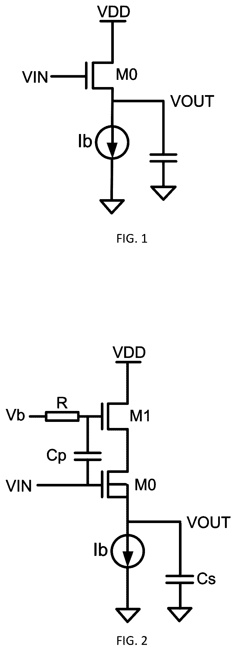
Referring to , a traditional source follower includes an NMOS transistor M 0 and a constant current source Ib. An input signal VIN is connected to a gate of M 0 , an output signal VOUT is output through a source of M 0 , the constant current source Ib is connected to the source of M 0 , and a drain of M 0 is connected to a supply voltage VDD. For a sampling network inside the chip, when the frequency of the input signal is low, the dominant factor for high linearity is a large output impedance provided by the constant current source in the follower, and when the frequency of the input signal is high, the dominant factor for high linearity is a large output current provided by the constant current source in the follower; the two requirements are usually contradictory to each other, because for a constant current source with a MOS transistor, a large output impedance means a small current, and a large current usually leads to a small output impedance. The traditional source follower usually include two NMOS transistors connected in series. One advantage of this structure is that the structure is very simple, and the NMOS transistors as the input transistor can provide a large trans-conductance, and the NMOS transistors as the constant current source can provide a large output impedance, but a disadvantage of this structure is that substrates of the NMOS transistor as the input transistor are grounded, and when the amplitude of the input signal changes greatly, the input transistor will be impacted by a very serious substrate bias effect, changing the threshold voltage of the input transistor, thus affecting the linearity of the whole follower. In order to alleviate the above problem, a substrate bias circuit was introduced into the follower, in which the substrate of a first input transistor is no longer directly grounded, but connected to a source of a second input transistor of another source follower with the same structure, which causes the substrate voltage of the first input transistor to vary with the source voltage of second the input transistor, greatly alleviating the previously described substrate bias effect of the input transistor, and significantly reducing the variation of the threshold voltage of the input transistor; compared with the first traditional structure, the linearity of this structure is significantly improved. However, when acting as a constant current source, NMOS transistors have drain voltages that vary continuously with the input voltage, and currents that vary continuously due to the NMOS transistors' channel length modulation effect, which reduces the output impedance of the NMOS transistors as a constant current source and also affects the linearity of the whole follower.
In order to describe the above problem in more detail, the working principle of the above two types of source followers and their respective advantages and disadvantages are analyzed below.
The structure [ 1 ] is a traditional source follower, as shown in , including NMOS transistors M 0 , M 1 , a resistor R, a capacitor Cp, and a constant current source Ib. An input signal VIN is connected to a gate of M 0 and one terminal of the capacitor Cp, and a source of M 0 is used as a signal output of the source follower, and is connected to one terminal of the constant-current source Ib and the sampling capacitor Cs; the other terminal of the constant-current source Ib is grounded. A drain of M 0 is connected to a source of M 1 , and a substrate of M 0 is connected to the source of M 0 . A gate of M 1 is connected to the other terminal of the capacitor Cp and one terminal of the resistor R, and the other terminal of the resistor R is connected to a common mode voltage Vb. When the follower operates normally, a bias voltage Vb is provided to the gate of M 1 through the resistor R. When the input signal VIN changes, the change of VIN is coupled to the gate of M 1 through an RC network including the resistor R and the capacitor Cp, and then changes in the gate voltage of M 1 are transmitted to the source of M 1 . Thereby, the source voltage of M 1 (i.e., drain voltage of M 0 ) is able to vary with VIN, and at the same time, the source voltage of M 0 varies with VIN, so that the drain voltage of M 0 can vary with the source voltage of M 0 . Therefore, the drain-source voltage Vds of M 0 can be kept constant, which suppresses the variation of the output impedance of the source follower and improves the accuracy of the source follower.
The structure [ 2 ] is another source follower, as shown in , which includes NMOS transistors M 0 , M 1 , capacitors C 1 and C 2 , switches S 1 and S 2 , and a constant current source Ib. An input signal VIN is connected to a gate of M 0 and one terminal of the capacitor C 2 , a source of M 0 is a signal output of the source follower, the source of M 0 is connected to one terminal of the constant-current source Ib and the sampling capacitor Cs, and the other terminal of the constant-current source Ib is grounded. A drain of M 0 is connected to a source of M 1 , and a substrate of M 0 is connected to the source of M 0 . Vb is a bias voltage, Vcom is a common mode voltage of the input signal, and a gate of M 1 is connected to the other terminal of the capacitor C 2 . The switches S 1 and S 2 alternately conduct and disconnect to provide bias voltage to the gate of M 1 , while C 2 acts as a coupling capacitor to couple the change of VIN to the gate of M 1 and then to the drain of M 0 , so that the drain-source voltage Vds of M 0 can be kept constant, which suppresses the change of the output impedance of the source follower and improves the accuracy of the source follower.
However, structure [ 1 ] and structure [ 2 ] have the same drawback that the drain voltage of M 0 varies with VIN, and there is a mismatch between the change of VIN and the change of M 0 source voltage; as a result, the drain-source voltage of M 0 has a poor stability, and therefore the output impedance of M 0 also has a poor stability. Meanwhile, the substrate and source of M 0 are connected to eliminate the substrate-bias effect of M 0 , but it also increases the parasitic capacitance of the source of M 0 , which further affects the accuracy of the source follower.
Referring to , the present disclosure provides a differential-follower control circuit, including a follower, an output-voltage following module, and a substrate-voltage following module.
In one embodiment, the follower includes a first MOS transistor M 0 , a second MOS transistor M 1 , and a constant current source Ib.
In an embodiment, the output-voltage following module may include a second constant current source Ib 1 and a voltage following unit, wherein the voltage following unit may be an RC circuit, and specifically, an RC network consisting of a resistor R and a compensation capacitor Cp connected in parallel.
In one embodiment, the substrate-voltage following module includes a third MOS transistor M 2 and a third constant current source Ib 2 .
In an embodiment, voltage output by the source of the first MOS transistor M 0 may be used to drive a sampling network to sample voltage inside the chip. The sampling network may include a sampling capacitor Cs.
In an embodiment, both the first MOS transistor and the second MOS transistor are NMOS transistors, and the third MOS transistor is a PMOS transistor.
Specifically, the input voltage VIN is connected to a gate of M 0 , a source of M 0 is connected to a positive terminal of Ib and one terminal of Cs, respectively, a negative terminal of Ib is grounded, and the other terminal of Cs is grounded; a drain of M 0 is connected to a source of M 1 , and a drain of M 1 is connected to a supply voltage VDD.
The parallel-connected resistor R and capacitor Cp has two common terminals, one of which is connected to the source of M 0 and the other to a gate of M 1 and a negative terminal of Ib 1 respectively, and a positive terminal of Ib 1 is connected to the supply voltage VDD.
A gate of M 2 is connected to the input voltage VIN and the gate of M 0 , a drain of M 2 is grounded, and a source of M 2 is connected to the substrate of M 0 and a negative terminal of Ib 2 , respectively.
The RC network consisting of the resistor R and the compensation capacitor Cp makes the gate voltage of M 1 vary with the output voltage VOUT of M 0 . Since the drain of M 0 is connected to the source of M 1 , the drain voltage of M 0 varies with the gate voltage of M 1 . By the above relationship, it can be seen that the drain voltage of M 0 can vary with the source voltage of M 0 . Therefore, it is possible to make the drain-source voltage difference Vds of the M 0 transistor not vary with the input signal VIN, thus, making the output impedance of the source of M 0 remain constant and improving the accuracy of the source follower of this structure.
In the traditional structures, the substrate and the source of M 0 are connected, thus eliminating the voltage difference between the substrate and the source of M 0 . However, one disadvantage of the traditional structures is that they give the source of M 0 a large parasitic capacitance, which also affects the accuracy of the source follower. To solve this problem, the present disclosure introduces a substrate-voltage following module consisting of a PMOS transistor M 2 and a constant current source Ib 2 , as mentioned above. Since the gate of M 2 is connected to the input signal VIN and the source of M 2 is connected to the substrate of M 0 , the substrate voltage of M 0 is able to vary with the input signal VIN; there is no increase in the parasitic capacitance of the source of M 0 while eliminating the substrate bias effect of M 0 , since the source of M 0 is not connected to its substrate. Thus, suppression of the substrate bias effect of M 0 in the source follower is effectively achieved by the present disclosure, and the accuracy of the source follower is improved.
In an embodiment, the aforementioned structures are designed under 40 nm CMOS process, and in the three different types of followers as shown in , corresponding parts have the same structures and dimensions, and load transistors in the three different types of followers also have the same structure and dimensions. In the present disclosure, the capacitor Cp of the follower has a capacitance of 0.2 pF, the resistor R has a resistance of 10KΩ, the sampling capacitor Cs has a capacitance of 0.3 pF, the supply voltage VDD is 1.2V, and the input bias voltage VIN is 0.6V. Comparison of simulation results of the spurious-free dynamic ranges (SFDR) of the different types of followers with the SFDR varying with the frequency of an input signal is shown in , where the horizontal coordinate is the frequency of the input signal and the vertical coordinate is the SFDR. From , it can be seen that the present disclosure improves the SFDR by about 6.1 dB when the input frequency is low and by about 5.8 dB when the input frequency is high, compared with the traditional structure [ 1 ] and the traditional structure [ 2 ]. Comparison of simulation results of the spurious-free dynamic ranges (SFDR) of the different types of followers with the SFDR varying with the amplitude of an input signal is shown in , where the horizontal coordinate is the amplitude of the input signal and the vertical coordinate is the SFDR. From , it can be seen that the present disclosure improves the SFDR by about 8 dB when the amplitude of the input signal is low and by about 6 dB when the amplitude of the input signal is high, compared with the traditional structure [ 1 ] and the traditional structure [ 2 ].
In summary, in the differential-follower control circuit provided by the present disclosure, the drain voltage of M 0 varies with VOUT instead of VIN, unlike the traditional structures, therefore significantly improving the stability of the drain-source voltage difference of M 0 and the accuracy of the source follower of this structure; the substrate voltage of M 0 can vary with the input signal VIN through M 2 and the constant current source Ib 2 , which stabilizes the substrate-source voltage difference Vbs of M 0 , eliminating the substrate bias effect of M 0 without increasing the parasitic capacitance of the source of M 0 , which is more advantageous in high-speed applications and improves the accuracy of the source follower; the drain-source voltage difference Vds and the substrate-source voltage difference Vbs of M 0 do not vary with the input signal VIN, which obviously improves the accuracy of the source follower, and at the same time, the source follower of the present disclosure does not introduce other non-ideal factors, thus significantly improving the performance of the source follower. Therefore, the present disclosure effectively overcomes various shortcomings of the prior art and has a high value for industrial application.
The above-mentioned embodiments only exemplarily illustrate the principles and effects of the present disclosure, but are not used to limit the present disclosure. Any person skilled in the art may modify or change the above embodiments without violating the spirit and scope of the present disclosure. Therefore, all equivalent modifications or changes made by those skilled in the art without departing from the spirit and technical concepts disclosed by the present disclosure should still be covered by the attached claims of the present disclosure.
Figures (3)
Citations
This patent cites (2)
- US10141897
- US2010/0225379