Series Capacitor Step-down Converter, Controller Circuit Thereof, and Control Method
Abstract
Provided is a controller circuit of a series capacitor step-down converter, the series capacitor step-down converter including an input line and an output line, a first switch, a coupled inductor, a second switch, a series capacitor, a third switch, a fourth switch, and an output capacitor, the controller circuit being configured to alternately switch between a first state in which the first switch and the fourth switch are on and a second state in which the second switch and the third switch are on while interposing a dead time between the first state and the second state, and turn on the second switch ahead of the third switch before a direction of a current of the first inductor is reversed in the dead time during a transition from the first state to the second state.
Claims (13)
1. A controller circuit of a series capacitor step-down converter, the series capacitor step-down converter including an input line and an output line, a first switch having a first terminal connected to the input line, a coupled inductor including a first inductor and a second inductor each having a first terminal connected to the output line, a second switch connected between a second terminal of the first inductor and a ground, a series capacitor connected between a second terminal of the first switch and the second terminal of the first inductor, a third switch connected between the second terminal of the first switch and a second terminal of the second inductor, a fourth switch connected between the second terminal of the second inductor and the ground, and an output capacitor connected to the output line, the controller circuit being configured to alternately switch between a first state in which the first switch and the fourth switch are on and a second state in which the second switch and the third switch are on while interposing a dead time between the first state and the second state, and turn on the second switch ahead of the third switch before a direction of a current of the first inductor is reversed in the dead time during a transition from the first state to the second state.
9. A control method of a series capacitor step-down converter, the series capacitor step-down converter including an input line and an output line, a first switch having a first terminal connected to the input line, a coupled inductor including a first inductor and a second inductor each having a first terminal connected to the output line, a second switch connected between a second terminal of the first inductor and a ground, a series capacitor connected between a second terminal of the first switch and the second terminal of the first inductor, a third switch connected between the second terminal of the first switch and a second terminal of the second inductor, a fourth switch connected between the second terminal of the second inductor and the ground, and an output capacitor connected to the output line, the control method comprising: a first step of alternately switching between a first state in which the first switch and the fourth switch are on and a second state in which the second switch and the third switch are on while interposing a dead time between the first state and the second state; and a second step of turning on the second switch ahead of the third switch before a direction of a current of the first inductor is reversed in the dead time during a transition from the first state to the second state.
Show 11 dependent claims
2. The controller circuit according to claim 1 , wherein the controller circuit turns on the second switch when a voltage of a connection node between the series capacitor and the second switch falls below a predetermined threshold voltage in the dead time.
3. The controller circuit according to claim 1 , wherein the controller circuit turns on the second switch when a voltage of a connection node between the third switch and the fourth switch exceeds a predetermined threshold voltage in the dead time.
4. The controller circuit according to claim 1 , wherein the controller circuit turns on the second switch when a current flowing through the first inductor in a direction of flowing to the output capacitor falls below a predetermined threshold value in the dead time.
5. The controller circuit according to claim 1 , wherein the controller circuit turns on the second switch when a current flowing through the second inductor in a direction of flowing in from the output capacitor exceeds a predetermined threshold value in the dead time.
6. The controller circuit according to claim 1 , wherein the fourth switch has a same withstand voltage as the first switch and the second switch.
7. The controller circuit according to claim 1 , wherein the controller circuit is integrally integrated on one semiconductor substrate.
8. A series capacitor step-down converter comprising: a main circuit of the series capacitor step-down converter; and the controller circuit according to claim 1 , the controller circuit being configured to drive the first to fourth switches included in the main circuit.
10. The control method according to claim 9 , wherein the second step includes turning on the second switch when a voltage of a connection node between the first switch and the second switch falls below a predetermined threshold voltage in the dead time.
11. The control method according to claim 9 , wherein the second step turns on the second switch when a voltage of a connection node between the third switch and the fourth switch exceeds a predetermined threshold voltage in the dead time.
12. The control method according to claim 9 , wherein the second step turns on the second switch when a current flowing through the first inductor in a direction of flowing to the output capacitor falls below a predetermined threshold value in the dead time.
13. The control method according to claim 9 , wherein the second step turns on the second switch when a current flowing through the second inductor in a direction of flowing in from the output capacitor exceeds a predetermined threshold value in the dead time.
Full Description
Show full text →
CROSS REFERENCE TO RELATED APPLICATIONS
This application claims priority benefit of Japanese Patent Application No. JP 2022-106109 filed in the Japan Patent Office on Jun. 30, 2022. Each of the above-referenced applications is hereby incorporated herein by reference in its entirety.
BACKGROUND
The present disclosure relates to a series capacitor converter.
A direct current (DC)/DC converter having a step-down function is used to generate a voltage lower than an input voltage. Known as the DC/DC converter having the step-down function are a step-down (Buck) type, a step-up/down type, a Cuk type, a Zeta type, a Sepic type, and the like.
Depending on applications, an interleaved type or a series capacitor type as a variation of a step-down converter is employed. The interleaved type is obtained by connecting Buck converters in parallel with each other, and commonly connecting inputs thereof and commonly connecting outputs thereof. A high-efficiency operation is realized by interleaved operation of a plurality of Buck converters. The interleaved type has a same step-down ratio as an ordinary buck converter.
A step-down converter of the series capacitor type can be considered to be a modification of the interleaved type in which the number of phases is two. The step-down converter of the series capacitor type has a configuration to which a series capacitor is added. The step-down converter of the series capacitor type can reduce the step-down ratio to ½ times that of the interleaved type, and is therefore suitable for an application that requires a small step-down ratio.
An example of the related art is disclosed in “Stefano Saggini, Shuai Jiang, Mario Ursino, Chenhao Nan, ‘A99% Efficient Dual-Phase Resonant Switched-Capacitor-Buck Converter for 48 V Data Center Bus Conversions,’ 2019 IEEE Applied Power Electronics Conference and Exposition (APEC).”
BRIEF DESCRIPTION OF THE DRAWINGS
is a circuit diagram of a series capacitor step-down converter according to an embodiment;
is an equivalent circuit diagram of the series capacitor step-down converter (main circuit) in a first state φ 1 ;
is an equivalent circuit diagram of the series capacitor step-down converter (main circuit) in a second state φ 2 ;
is a current waveform chart of the series capacitor step-down converter;
is a current waveform chart of the series capacitor step-down converter;
is a timing diagram of assistance in explaining operation of the series capacitor step-down converter with dead times taken into consideration;
is a timing diagram of assistance in explaining operation of the series capacitor step-down converter;
is a circuit diagram illustrating the voltages and currents of respective nodes in a dead time T D1 ;
is a timing diagram of assistance in explaining a problem that can occur in the series capacitor step-down converter;
is a circuit diagram illustrating the voltages and currents of the respective nodes in an interval Tc;
is a timing diagram of assistance in explaining control of the series capacitor step-down converter by a controller IC according to the embodiment;
is a diagram illustrating the voltages and currents of the respective nodes in an interval Tc′ in which a second switch is on, I L1 <0, and I L2 <0;
is a circuit diagram illustrating an example of a configuration of the controller IC according to the embodiment;
is a waveform chart of assistance in explaining operation of a timing generator; and
is a diagram illustrating an example of an electronic apparatus including the series capacitor step-down converter.
DETAILED DESCRIPTION
Outline of Embodiments
An outline of a few illustrative embodiments of the present disclosure will be described. This outline describes, in a simplified manner, a few concepts of one or a plurality of embodiments as an introduction to the following detailed description for a purpose of basic understanding of the embodiments, and does not limit the scope of the disclosure. This outline is neither a comprehensive outline of all conceivable embodiments nor intended to identify important elements of all of the embodiments or demarcate the scope of a part or all of aspects. For convenience, “one embodiment” may be used to refer to one embodiment (an example or a modification) or a plurality of embodiments (examples or modifications) disclosed in the present specification.
A controller circuit according to one embodiment controls a series capacitor step-down converter. The series capacitor step-down converter includes an input line and an output line, a first switch having a first terminal connected to the input line, a coupled inductor including a first inductor and a second inductor each having a first terminal connected to the output line, a second switch connected between a second terminal of the first inductor and a ground, a series capacitor connected between a second terminal of the first switch and the second terminal of the first inductor, a third switch connected between the second terminal of the first switch and a second terminal of the second inductor, a fourth switch connected between the second terminal of the second inductor and the ground, and an output capacitor connected to the output line. The controller circuit alternately switches between a first state in which the first switch and the fourth switch are on and a second state in which the second switch and the third switch are on while interposing a dead time between the first state and the second state, and turns on the second switch before a direction of a current of the first inductor is reversed in the dead time during a transition from the first state to the second state.
In the dead time, when the direction of the current of the first inductor is reversed from a direction of flowing into the output capacitor to an opposite direction therefrom, the drain voltage of the second switch rises, and the voltage of a connection node between the third switch and the first switch rises to the vicinity of an input voltage. As a result, a current flowing through the second inductor charges the capacitance of the fourth switch, and raises the drain-to-source voltage of the fourth switch to the vicinity of the input voltage. In the above-described configuration, the second switch is turned on before the direction of the current of the first inductor is reversed. It is thereby possible to suppress a rise in the drain voltage of the second switch, and suppress a rise in the drain voltage of the fourth switch.
In one embodiment, the controller circuit may turn on the second switch when a voltage of a connection node between the series capacitor and the second switch falls below a predetermined threshold voltage in the dead time. Thus, the second switch can be turned on before the direction of the current of the first inductor is reversed.
In one embodiment, the controller circuit may turn on the second switch when a voltage of a connection node between the third switch and the fourth switch exceeds a predetermined threshold voltage in the dead time. Thus, the second switch can be turned on before the direction of the current of the first inductor is reversed.
In one embodiment, the controller circuit may turn on the second switch when a current flowing through the first inductor in a direction of flowing to the output capacitor falls below a predetermined threshold value in the dead time. Thus, the second switch can be turned on before the direction of the current of the first inductor is reversed.
In one embodiment, the controller circuit may turn on the second switch when a current flowing through the second inductor in a direction of flowing in from the output capacitor exceeds a predetermined threshold value in the dead time. Thus, the second switch can be turned on before the direction of the current of the first inductor is reversed.
In one embodiment, the fourth switch may have a same withstand voltage as the first switch and the second switch. In general, a low withstand voltage element has a lower on resistance than a high withstand voltage element. Accordingly, efficiency can be improved by using an element having a low withstand voltage as the fourth switch.
In one embodiment, the controller circuit may be integrally integrated on one semiconductor substrate. “Integrally integrated” includes a case where all of circuit constituent elements are formed on the semiconductor substrate and a case where main circuit constituent elements are integrally integrated. A part of resistances, capacitors, and the like may be provided on the outside of the semiconductor substrate for adjustment of circuit constants. Integrating the circuit on one chip can reduce a circuit area and hold characteristics of the circuit elements uniform.
In one embodiment, a series capacitor step-down converter may include a main circuit and the controller circuit that drives the first to fourth switches included in the main circuit.
Embodiment
A preferred embodiment will hereinafter be described with reference to the drawings. Identical or equivalent constituent elements, members, and processing illustrated in each drawing are identified by the same reference signs, and repeated description thereof will be omitted as appropriate. In addition, the embodiment is not restrictive of the disclosure but is illustrative, and all features described in the embodiment and combinations thereof are not necessarily substantial to the disclosure.
In the present specification, a “state in which a member A is connected to a member B” includes not only a case where the member A and the member B are physically directly connected to each other but also a case where the member A and the member B are indirectly connected to each other via another member that does not substantially affect a state of electric connection between the member A and the member B or does not impair functions or effects produced by the coupling of the member A and the member B.
Similarly, a “state in which a member C is connected (provided) between the member A and the member B” includes not only a case where the member A and the member C or the member B and the member C are directly connected to each other but also a case where the member A and the member C or the member B and the member C are indirectly connected to each other via another member that does not substantially affect a state of electric connection between the member A and the member C or the member B and the member C or does not impair functions or effects produced by the coupling of the member A and the member C or the member B and the member C.
In addition, in the present specification, reference signs given to electric signals such as voltage signals, or current signals, or circuit elements such as resistances, capacitors, or inductors represent respective voltage values, current values, or circuit constants (resistance values, capacitance values, or inductances) as required.
Axes of ordinates and axes of abscissas in waveform charts and timing diagrams referred to in the present specification are enlarged or reduced as appropriate in order to facilitate understanding, and each waveform illustrated therein is simplified or exaggerated or emphasized in order to facilitate understanding.
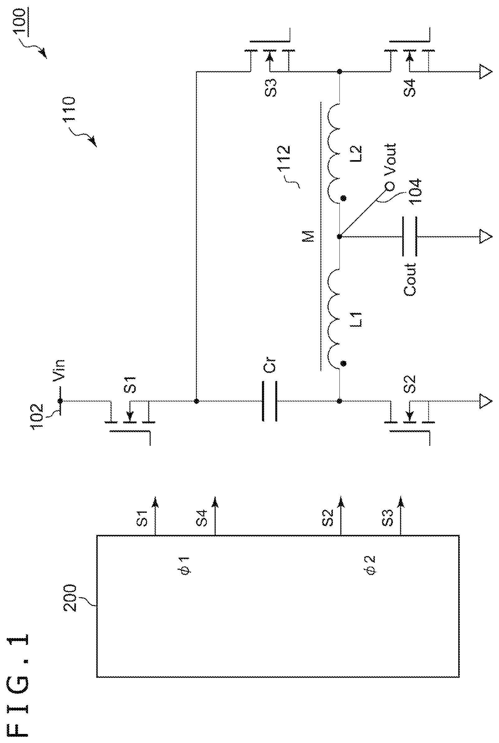
is a circuit diagram of a series capacitor step-down converter 100 according to the embodiment. The series capacitor step-down converter 100 steps down an input voltage Vin supplied to an input line 102 , and generates an output voltage Vout after the step-down at an output line 104 .
The series capacitor step-down converter 100 includes a main circuit 110 and a controller integrated circuit (IC) 200 . The controller IC 200 is an application specific integrated circuit (ASIC) integrated on one semiconductor substrate.
The main circuit 110 includes first to fourth switches S 1 to S 4 , a coupled inductor 112 , a series capacitor Cr, and an output capacitor Cout.
The first switch S 1 has a first terminal connected to the input line 102 . The coupled inductor 112 is a transformer. The coupled inductor 112 includes a first inductor L 1 and a second inductor L 2 that are magnetically coupled to each other. The first inductor L 1 and the second inductor L 2 have a same inductance L, and have a mutual inductance M. A first terminal of each of the first inductor L 1 and the second inductor L 2 is connected to the output line 104 .
The second switch S 2 is connected between a second terminal of the first inductor L 1 and a ground. The series capacitor Cr is connected between a second terminal of the first switch S 1 and the second terminal of the first inductor L 1 . The third switch S 3 is connected between the second terminal of the first switch S 1 and a second terminal of the second inductor L 2 . The fourth switch S 4 is connected between the second terminal of the second inductor L 2 and the ground. The output capacitor Cout is connected between the output line 104 and the ground.
In the present example, the first to fourth switches S 1 to S 4 are all illustrated as N-channel metal-oxide-semiconductor field-effect transistors (MOSFETs). However, there is no limitation to this. Other transistors may be used as the first to fourth switches S 1 to S 4 . In addition, the second switch S 2 and the fourth switch S 4 on a lower side may be rectifying elements such as diodes.
The controller IC 200 controls the first to fourth switches S 1 to S 4 to generate an output voltage Vout at the output line 104 . Specifically, the controller IC 200 alternately repeats a first state φ 1 and a second state φ 2 at a predetermined switching frequency f SW while interposing a dead time T D between the first state φ 1 and the second state φ 2 .
•
• First State φ 1 : • First Switch S 1 =ON • Second Switch S 2 =OFF • Third Switch S 3 =OFF • Fourth Switch S 4 =ON • Second State φ 2 : • First Switch S 1 =OFF • Second Switch S 2 =ON • Third Switch S 3 =ON • Fourth Switch S 4 =OFF • Dead Time T D : • First Switch S 1 =OFF • Second Switch S 2 =OFF • Third Switch S 3 =OFF • Fourth Switch S 4 =OFF
As required, a dead time in a process of a transition from the first state φ 1 to the second state φ 2 will be distinguished by being provided with a suffix T D1 , and a dead time in a process of a transition from the second state φ 2 to the first state φ 1 will be distinguished by being provided with a suffix T D2 .
When the length of each of the first state φ 1 and the second state φ 2 is T ON , the switching frequency f SW is 1/(2×T ON ). In other words, operation at the switching frequency f SW refers to repeating the first state φ 1 and the second state φ 2 having a length of T ON =1/(2×f SW ).
The above is a configuration of the series capacitor step-down converter 100 . Operation thereof will next be described.
is an equivalent circuit diagram of the series capacitor step-down converter 100 (main circuit 110 ) in the first state φ 1 . The switches S 1 and S 4 in an on state are represented as mere wiring. In addition, the coupled inductor 112 is represented as an equivalent circuit including an exciting inductance Lm and a leakage inductance Lk. A current flowing through the first inductor L 1 will be referred to as a first coil current I L1 . A current flowing through the second inductor L 2 will be referred to as a second coil current I L2 .
In the first state φ 1 , the series capacitor Cr, the first inductor L 1 (leakage inductance Lk), and the output capacitor Cout form a series resonant circuit, and a resonance current Ires flows through the first inductor L 1 (I L1 =Ires). A total current of a resonance current Ires′ as a replica of the resonance current Ires flowing through the first inductor L 1 and an exciting current Im 2 flowing through the exciting inductance Lm flows through the second inductor L 2 . Thus, the second coil current I L2 is I L2 =Ires′+Im 2 .
is an equivalent circuit diagram of the series capacitor step-down converter 100 (main circuit 110 ) in the second state φ 2 . The switches S 2 and S 3 in an on state are represented as mere wiring.
In the second state φ 2 , the series capacitor Cr, the leakage inductance Lk, and the output capacitor Cout form a series resonant circuit, and a resonance current Ires flows through the second inductor L 2 (I L2 =Ires). A total current of a resonance current Ires′ as a replica of the resonance current Ires flowing through the second inductor L 2 and an exciting current Im 1 flowing through the exciting inductance Lm flows through the first inductor L 1 . Thus, the first coil current I L1 is I L1 =Ires′+Im 1 .
When the first state φ 1 and the second state φ 2 are alternately repeated, in a steady state, a voltage across the series capacitor Cr is Vin/2, and a remaining Vin/2 is applied to the coupled inductor 112 . When the inductances of the first inductor L 1 and the second inductor L 2 are equal to each other, the output voltage Vout that is ¼ times Vin occurs at the output line 104 .
Conditions for the series capacitor step-down converter 100 to perform zero voltage switching (ZVS) are as follows.
•
• A transition from the first state φ 1 to the second state φ 2
When I L1 ≥0 during a dead time T D immediately after the first state φ 1 , the current I L1 flows through a body diode of the second switch S 2 , and a voltage across the second switch S 2 is decreased. At this time, when a transition is made to the second state φ 2 , that is, when the second switch S 2 is turned on, ZVS of the second switch S 2 is effected. Incidentally, the currents I L1 and I L2 have a direction of going to the output line 104 as a positive direction.
In addition, when I L2 <0 during the dead time T D , a regenerative current raises the voltage of a connection node between the third switch S 3 and the fourth switch S 4 , and decreases a voltage across the third switch S 3 . At this time, when a transition is made to the second state φ 2 , that is, when the third switch S 3 is turned on, ZVS of the third switch S 3 is effected.
•
• A transition from the second state φ 2 to the first state φ 1
When I L1 <0 during a dead time T D immediately after the second state φ 2 , a regenerative current raises the voltage of a connection node between the first switch S 1 and the second switch S 2 , and decreases a voltage across the first switch S 1 . At this time, when a transition is made to the first state φ 1 , that is, when the first switch S 1 is turned on, ZVS of the first switch S 1 is effected.
In addition, when I L2 ≥0 during the dead time, the current I L2 flows through a body diode of the fourth switch S 4 , and a voltage across the fourth switch S 4 is decreased. At this time, when a transition is made to the first state φ 1 , that is, when the fourth switch S 4 is turned on, ZVS of the fourth switch S 4 is effected.
is a current waveform chart of the series capacitor step-down converter 100 . The switching frequency f SW coincides with a resonance frequency f 0 of the main circuit 110 , and a transition is made between the first state φ 1 and the second state φ 2 in timing in which the resonance current Ires becomes zero. Here, the dead time is omitted. illustrates current waveforms in a case where the first to fourth switches S 1 to S 4 are assumed to be ideal switches, that is, in a case where the first to fourth switches S 1 to S 4 do not include a parasitic capacitance.
In timing of an end of the first state φ 1 , the current I L1 of the first inductor L 1 is positive or zero (I L1 ≥0), and the current I L2 of the second inductor L 2 is negative (I L2 <0). The above-described ZVS conditions are therefore satisfied.
Similarly, in timing of an end of the second state φ 2 , the current I L1 of the first inductor L 1 is negative (I L1 <0), and the current I L2 of the second inductor L 2 is positive or zero (I L2 ≥0). The above-described ZVS conditions are therefore satisfied.
Thus, the series capacitor step-down converter 100 can satisfy the ZVS conditions by switching at the resonance frequency f 0 . The series capacitor step-down converter 100 can therefore perform high-efficiency operation.
is a current waveform chart of the series capacitor step-down converter 100 . illustrates waveforms with the parasitic capacitances of the MOSFETs ignored. In actuality, however, the parasitic capacitances are present. The parasitic capacitances suppress current discontinuity straddling a dead time. The coil currents I L1 and I L2 become continuous, and the coil currents I L1 and I L2 in the first state φ 1 and the second state φ 2 have symmetric waveforms on a time axis with respect to the dead time.
is a timing diagram of assistance in explaining operation of the series capacitor step-down converter 100 with dead times taken into consideration. illustrates operation in a case where the switching frequency f SW is equal to the resonance frequency f 0 , and each of the lengths T ON of the first state φ 1 and the second state φ 2 is ½ of a resonance period T r (=1/f r ).
Consideration will be given to an operation mode in which the switching frequency f SW is higher than the resonance frequency f 0 of the main circuit 110 (f SW >f 0 ).
is a timing diagram of assistance in explaining operation of the series capacitor step-down converter 100 . is a circuit diagram illustrating the voltages and currents of respective nodes in a dead time T D1 . A connection node between the first switch S 1 and the series capacitor Cr will be referred to as a first node N 1 . A connection node between the series capacitor Cr and the second switch S 2 will be referred to as a second node N 2 . A connection node between the third switch S 3 and the fourth switch S 4 will be referred to as a third node N 3 . A voltage V N2 of the second node N 2 is a drain-to-source voltage Vds 2 of the second switch S 2 . A voltage V N3 of the third node N 3 is a drain-to-source voltage Vds 4 of the fourth switch S 4 .
A reference will be made to . The dead time T D1 includes two intervals Ta and Tb. illustrates, in order from a top, a state of the first switch S 1 and the fourth switch S 4 , a state of the second switch S 2 and the third switch S 3 , the currents I L1 and I L2 flowing through the first inductor L 1 and the second inductor L 2 , the respective drain-to-source voltages Vds of the first switch S 1 and the third switch S 3 , and the respective drain-to-source voltages Vds of the second switch S 2 and the fourth switch S 4 . The currents I L1 and I L2 have a direction of flowing into the output capacitor Cout as a positive direction.
In the first state φ 1 , the first switch S 1 is on. Therefore, the drain-to-source voltage Vds 1 of the first switch S 1 is 0 V, and a voltage V N1 of the first node N 1 is equal to the input voltage Vin. In addition, the fourth switch S 4 is on. Therefore, the drain-to-source voltage Vds 4 of the fourth switch S 4 is 0 V, and the voltage V N3 of the third node N 3 is 0 V.
In the steady state, a voltage Vc of the series capacitor Cr is Vin/2. The voltage V N2 of the second node N 2 is lower than the voltage V IN (=Vin) of the first node N 1 by Vc (=Vin/2), and is therefore Vin/2. Hence, the drain-to-source voltage Vds 2 of the second switch S 2 is Vin/2.
When the dead time T D1 arrives, the first to fourth switches S 1 to S 4 are turned off. In a first half Ta of the dead time T D1 , I L1 >0 and I L2 >0. When the second switch S 2 is turned off, the current I L1 flows through the body diode of the second switch S 2 , the parasitic capacitance of the second node N 2 (drain-to-source capacitance of the second switch S 2 ) is discharged, and the voltage V N2 (that is, Vds 2 ) of the second node N 2 decreases from Vin/2 to 0 V.
The voltage V N1 of the first node N 1 is higher than the voltage V N2 of the second node N 2 by the voltage Vc (=Vin/2) of the series capacitor Cr. Hence, in the interval Ta, the voltage V N1 of the first node N 1 changes from Vin to Vin/2. At this time, the drain-to-source voltage Vds 1 of the first switch S 1 increases from 0 V to Vin/2.
The current I L2 of the second inductor L 2 flows through the body diode of the fourth switch S 4 . The drain-to-source voltage Vds 4 of the fourth switch S 4 is therefore maintained at 0 V or in the vicinity thereof. The drain-to-source voltage Vds 3 of the third switch S 3 is a potential difference between the first node N 1 and the third node N 3 , and therefore changes from Vin to Vin/2.
When a second half Tb of the dead time T D1 arrives, the current I L2 of the second inductor L 2 is inverted (I L2 <0). Then, the current I L2 flows through a body diode of the third switch S 3 , and charges the parasitic capacitance of the third node N 3 (drain-to-source capacitance of the fourth switch S 4 ). As a result, the voltage V N3 of the third node N 3 rises from 0 V to Vin/2, and the drain-to-source voltage Vds 3 of the third switch S 3 decreases to 0 V.
In the interval Tb, the drain-to-source voltage Vds 4 of the fourth switch S 4 increases from 0 V to Vin/2.
Directing attention to , the drain-to-source voltages Vds 1 , Vds 2 , and Vds 4 of the first switch S 1 , the second switch S 2 , and the fourth switch S 4 each change between 0 and Vin/2. Hence, when the operation waveforms of are maintained, it suffices for the first switch S 1 , the second switch S 2 , and the fourth switch S 4 to be constituted by elements having a withstand voltage of Vin/2, and it suffices for only the third switch S 3 to be constituted by an element having a withstand voltage of Vin.
The present inventors have investigated operation in dead time periods and have come to recognize the following problem. It is to be noted that this problem is not to be recognized as an ordinary one for those skilled in the art.
is a timing diagram of assistance in explaining a problem that can occur in the series capacitor step-down converter 100 . In this timing diagram, the dead time T D1 includes three intervals Ta, Tb, and Tc. is a circuit diagram illustrating the voltages and currents of the respective nodes in the interval Tc.
When the dead time T D1 is lengthened, the direction of the current I L1 flowing through the first inductor L 1 is reversed (I L1 <0), and the interval Tc is started. In the interval Tc, the current I L1 flowing through the first inductor L 1 in an opposite direction raises the voltage V N2 of the second node N 2 from 0 V to Vin/2. Then, the voltage V N1 of the first node N 1 is charged by the current I L2 passing through the body diode of the third switch S 3 , and increases from Vin/2 to Vin. When the current I L2 flows through the body diode of the third switch S 3 , the voltage V N1 of the first node N 1 and the voltage V N3 of the third node N 3 are substantially equal to each other. The voltage V N3 of the third node N 3 therefore rises from Vin/2 to Vin.
Thus, when the direction of the current I L1 of the first inductor L 1 is reversed during the dead time T D1 , the voltage Vin is applied to the fourth switch S 4 in the interval Tc. Hence, in addition to the third switch S 3 , the fourth switch S 4 needs to be constituted by a high withstand voltage element.
In general, a low withstand voltage element has a lower on resistance and a better frequency characteristic than a high withstand voltage element. Therefore, when a design is made so as to tolerate the operation mode during the interval Tc, the on resistance of the fourth switch S 4 is increased, and consequently conversion efficiency is decreased.
The above is a problem that can occur in the series capacitor step-down converter 100 . In order to solve this problem, the controller IC 200 performs the following control.
is a timing diagram of assistance in explaining the control of the series capacitor step-down converter 100 by the controller IC 200 according to the embodiment.
In the dead time T D1 during a transition from the first state φ 1 to the second state φ 2 , the controller IC 200 turns on the second switch S 2 ahead of the third switch S 3 before time ti at which the direction of the current I L1 of the first inductor L 1 is reversed.
is a diagram illustrating the voltages and currents of the respective nodes in an interval Tc′ in which the second switch S 2 is on, I L1 <0, and I L2 <0. Because the second switch S 2 is on, the voltage V N2 of the second node N 2 is 0 V. The current I L1 flowing in the reverse direction flows through the second switch S 2 to the ground. Because the voltage V N2 of the second node N 2 is fixed at 0 V, the voltage of the first node N 1 is fixed at Vin/2. The current I L2 flows into the first node N 1 via the body diode of the third switch S 3 , and charges the series capacitor Cr.
The above is an operation of the series capacitor step-down converter 100 . According to this control, after the discharging of the second node N 2 has progressed to a certain degree, and the voltage V N2 of the second node N 2 has become sufficiently low, the second switch S 2 is turned on before the direction of the current I L1 is reversed. Consequently, the voltage V N3 of the third node N 3 changes in a range of 0 V to Vin/2, and can be prevented from rising to the input voltage Vin. This can prevent the application of a high voltage to the fourth switch S 4 .
As with the first switch S 1 and the second switch S 2 , the fourth switch S 4 can be constituted by an element having a withstand voltage of Vin/2. In that case, as compared with a case where the fourth switch S 4 is constituted by an element having a withstand voltage of Vin, the on resistance of the fourth switch S 4 can be reduced, so that the efficiency of the series capacitor step-down converter 100 can be improved.
Returning to , description will be made of timing of turning on the second switch S 2 . After a transition is made to the dead time T D1 at time to, it suffices to turn on the second switch S 2 after timing in which the voltage V N2 of the second node N 2 , that is, the drain-to-source voltage of the second switch S 2 is sufficiently decreased and before time ti at which the direction of the current I L1 is reversed.
is a circuit diagram illustrating an example of a configuration of the controller IC 200 according to the embodiment. The controller IC 200 includes drivers DR 1 to DR 4 , a control logic circuit 210 , an oscillator 220 , and a timing generator 230 .
The oscillator 220 generates a clock signal CLK that defines the switching frequency. The control logic circuit 210 alternately repeats the first state φ 1 and the second state φ 2 in synchronism with the clock signal CLK while interposing a dead time between the first state φ 1 and the second state φ 2 . The drivers DR 1 to DR 4 drive the corresponding switches S 1 to S 4 according to control signals generated by the control logic circuit 210 .
The timing generator 230 generates a timing signal S 2 _ON that gives an instruction for the timing of turning on the second switch S 2 . The control logic circuit 210 turns on the second switch S 2 when the timing signal S 2 _ON is asserted (for example, rendered high) in the dead time T D1 .
Several examples of operation of the timing generator 230 will be described.
is a waveform chart of assistance in explaining operation of the timing generator 230 . illustrates four operation examples as (i) to (iv).
(i) The timing generator 230 may, for example, monitor the voltage V N2 of the second node N 2 (that is, the drain-to-source voltage Vds 2 of the second switch S 2 ) and assert the timing signal S 2 _ON when the voltage V N2 of the second node N 2 becomes lower than (crosses) a threshold level V TH1 set in the vicinity 0 V, for example, between several tens mV and 200 mV. In this case, the timing generator 230 can be constituted by a voltage comparator.
(ii) The timing generator 230 may, for example, monitor the voltage V N3 of the third node N 3 (that is, the drain-to-source voltage Vds 4 of the fourth switch S 4 ) and assert the timing signal S 2 _ON when the voltage V N3 of the third node N 3 exceeds (crosses) a threshold voltage V TH2 set higher than 0 V and lower than Vin/2. In this case, the timing generator 230 can be constituted by a voltage comparator.
(iii) The timing generator 230 may, for example, directly monitor the current I L1 of the first inductor L 1 and assert the timing signal S 2 _ON when the current I L1 becomes smaller than a positive threshold current I TH1 in the vicinity of 0 A. In this case, the timing generator 230 may include a current detecting circuit that converts the current I L1 into a voltage signal and a voltage comparator that compares the voltage signal with a threshold voltage. A configuration of the current detecting circuit is not particularly limited. However, for example, a sense resistance may be inserted in series with the inductor L 1 , and a voltage drop across the sense resistance may be detected.
(iv) The timing generator 230 may, for example, monitor the current I L2 of the second inductor L 2 and assert the timing signal S 2 _ON when the current I L2 becomes smaller than a positive threshold current I TH2 . In this case, the timing generator 230 may include a current detecting circuit that converts the current I L2 into a voltage signal and a voltage comparator that compares the voltage signal with a threshold voltage.
(Applications)
is a diagram illustrating an example of an electronic apparatus 700 including the series capacitor step-down converter 100 . A suitable example of the electronic apparatus 700 is a server. Originally, a power supply line of 12 V has been led into the server. Internal circuits 710 are therefore designed to operate at 12 V. The internal circuits 710 can include a central processing unit (CPU), a memory, a local area network (LAN) interface circuit, a DC/DC converter that steps down the voltage of 12 V, and the like.
Recently, a move has been under way to change a bus voltage from 12 to 48 V in order to reduce a current flowing through a wire. In this case, a power supply circuit 720 that steps down a power supply voltage of 48 to 12 V is necessary. The series capacitor step-down converter 100 having a gain of ¼ times as described above can be suitably used as such a power supply circuit 720 .
The electronic apparatus 700 is not limited to the server, but the electronic apparatus 700 may be a vehicle-mounted apparatus. Automobile batteries of 12 V or 24 V are mainstream automobile batteries. However, there are cases where a 48-V system is employed in a hybrid vehicle. Also in this case, a power supply circuit that converts a battery voltage of 48 V to 12 V is necessary. In such a case, the ¼ times series capacitor step-down converter 100 can be used suitably.
Besides, the electronic apparatus 700 may be an industrial apparatus or an OA apparatus, or may be a consumer appliance such as an audio apparatus.
The embodiments are illustrative, and it is to be understood by those skilled in the art that there are various modifications to combinations of respective constituent elements and respective processing processes of these embodiments, and that such modifications are also included in the present disclosure and can constitute the scope of the present disclosure.
(Supplementary Notes)
(Item 1)
A controller circuit of a series capacitor step-down converter,
•
• the series capacitor step-down converter including
• an input line and an output line, • a first switch having a first terminal connected to the input line, • a coupled inductor including a first inductor and a second inductor each having a first terminal connected to the output line, • a second switch connected between a second terminal of the first inductor and a ground, • a series capacitor connected between a second terminal of the first switch and the second terminal of the first inductor, • a third switch connected between the second terminal of the first switch and a second terminal of the second inductor, • a fourth switch connected between the second terminal of the second inductor and the ground, and • an output capacitor connected to the output line, • the controller circuit being configured to
• alternately switch between a first state in which the first switch and the fourth switch are on and a second state in which the second switch and the third switch are on while interposing a dead time between the first state and the second state, and • turn on the second switch ahead of the third switch before a direction of a current of the first inductor is reversed in the dead time during a transition from the first state to the second state. (Item 2)
The controller circuit according to item 1, in which
•
• the controller circuit turns on the second switch when a voltage of a connection node between the series capacitor and the second switch falls below a predetermined threshold voltage in the dead time. (Item 3)
The controller circuit according to item 1, in which
•
• the controller circuit turns on the second switch when a voltage of a connection node between the third switch and the fourth switch exceeds a predetermined threshold voltage in the dead time. (Item 4)
The controller circuit according to item 1, in which
•
• the controller circuit turns on the second switch when a current flowing through the first inductor in a direction of flowing to the output capacitor falls below a predetermined threshold value in the dead time. (Item 5)
The controller circuit according to item 1, in which
•
• the controller circuit turns on the second switch when a current flowing through the second inductor in a direction of flowing in from the output capacitor exceeds a predetermined threshold value in the dead time. (Item 6)
The controller circuit according to any one of Items 1 to 5, in which
•
• the fourth switch has a same withstand voltage as the first switch and the second switch. (Item 7)
The controller circuit according to any one of items 1 to 6, in which
•
• the controller circuit is integrally integrated on one semiconductor substrate. (Item 8)
A series capacitor step-down converter including:
•
• a main circuit of the series capacitor step-down converter; and • the controller circuit according to any one of items 1 to 7, the controller circuit being configured to drive the first to fourth switches included in the main circuit. (Item 9)
A control method of a series capacitor step-down converter,
•
• the series capacitor step-down converter including
• an input line and an output line, • a first switch having a first terminal connected to the input line, • a coupled inductor including a first inductor and a second inductor each having a first terminal connected to the output line, • a second switch connected between a second terminal of the first inductor and a ground, • a series capacitor connected between a second terminal of the first switch and the second terminal of the first inductor, • a third switch connected between the second terminal of the first switch and a second terminal of the second inductor, • a fourth switch connected between the second terminal of the second inductor and the ground, and • an output capacitor connected to the output line, • the control method including: • a first step of alternately switching between a first state in which the first switch and the fourth switch are on and a second state in which the second switch and the third switch are on while interposing a dead time between the first state and the second state; and • a second step of turning on the second switch ahead of the third switch before a direction of a current of the first inductor is reversed in the dead time during a transition from the first state to the second state. (Item 10)
The control method according to item 9, in which
•
• the second step includes turning on the second switch when a voltage of a connection node between the first switch and the second switch falls below a predetermined threshold voltage in the dead time. (Item 11)
The control method according to item 9, in which
•
• the second step turns on the second switch when a voltage of a connection node between the third switch and the fourth switch exceeds a predetermined threshold voltage in the dead time. (Item 12)
The control method according to item 9, in which
•
• the second step turns on the second switch when a current flowing through the first inductor in a direction of flowing to the output capacitor falls below a predetermined threshold value in the dead time. (Item 13)
The control method according to item 9, in which
•
• the second step turns on the second switch when a current flowing through the second inductor in a direction of flowing in from the output capacitor exceeds a predetermined threshold value in the dead time.
According to a certain aspect of the present disclosure, the voltage applied to the fourth switch can be reduced.
Figures (15)
Citations
This patent cites (4)
- US2013/0154600
- US2021/0075323
- US2022/0115953
- US2023/0412079