Electronic Device Configured to Sense a Pen
Abstract
Disclosed is an electronic device including a sensor layer and a sensor driver. The sensor layer includes a plurality of first sensing electrodes, a plurality of first electrodes, a plurality of second sensing electrodes, a plurality of second electrodes, and a plurality of lines. The plurality of lines includes a first line electrically connected to one of the plurality of second sensing electrodes and in a first peripheral region, a second line electrically connected to another one of the plurality of second sensing electrodes and in a second peripheral region, wherein, in a sensing mode to sense an input of the pen, the sensor driver is configured to apply a first weighting value to a first sensing signal received from the first line and a second weighting value, different from the first weighting value, to a second sensing signal received from the second line.
Claims (11)
1. An electronic device comprising: a sensor layer including a peripheral region having a first peripheral region and second peripheral region, and a main region between the first peripheral region and the second peripheral region; and a sensor driver configured to drive the sensor layer, wherein the sensor layer further comprises: a plurality of first sensing electrodes arranged along a first direction; a plurality of first electrodes arranged along the first direction, and overlapping the plurality of first sensing electrodes, respectively; a plurality of second sensing electrodes arranged along a second direction crossing the first direction; and a plurality of lines in the peripheral region and comprising: a first line electrically connected to one of the plurality of second sensing electrodes and in the first peripheral region; a second line electrically connected to another one of the plurality of second sensing electrodes and in the second peripheral region, a third line connected to a first end of one of the plurality of first electrodes; and a fourth line connected to a second end of the one of the plurality of first electrodes, wherein, in a driving mode to generate a magnetic field for charging a pen, the sensor driver is configured to apply a first signal to the third line and a second signal, different from the first signal, to the fourth line at a first time, and wherein, in a sensing mode to sense an input of the pen, the sensor driver is configured to apply a first weighting value to a first sensing signal received from the first line and a second weighting value, different from the first weighting value, to a second sensing signal received from the second line.
Show 10 dependent claims
2. The electronic device of claim 1 , wherein each of the first weighting value and the second weighting value is at least one of a gain and a weight.
3. The electronic device of claim 2 , wherein the sensor driver is further configured to drive the sensor layer in a pre-pen sensing driving mode, and the sensor driver is configured to determine at least one of the gain or the weight applied to the first sensing signal and the second sensing signal.
4. The electronic device of claim 2 , wherein the sensor driver includes a charge voltage amplifier electrically connected to at least one of the plurality of second sensing electrodes, and a resistor and a capacitor, which are connected to an input terminal and an output terminal of the charge voltage amplifier, and wherein the sensor driver is further configured to adjust the gain by changing at least one of the resistor or the capacitor.
5. The electronic device of claim 2 , wherein the sensor driver includes an analog-to-digital converter electrically connected to at least one of the plurality of second sensing electrodes, and wherein the sensor driver is configured to apply the weight to a digital signal output from the analog-to-digital converter.
6. The electronic device of claim 2 , wherein the main region comprises a plurality of division areas defined along the first direction, and the sensor driver is further configured to: drive the sensor layer in a pre-pen sensing driving mode; and detect an active area of the sensor layer corresponding to the input from among the plurality of division areas that corresponds to a pen location according to the input.
7. The electronic device of claim 6 , wherein the sensor driver is further configured to adjust at least one of the gain or the weight applied to at least one of the first sensing signal or the second sensing signal according to a location of the active area.
8. The electronic device of claim 6 , wherein the main region comprises a first outer division area, a central division area, and a second outer division area aligned along the first direction, wherein the sensor driver is configured to control a first gain applied to the first sensing signal to be equal to a second gain applied to the second sensing signal based on the active area corresponding to the central division area, and wherein the sensor driver is configured to control a first weight applied to the first sensing signal to be equal to a second weight applied to the second sensing signal based on the active area corresponding to the central division area.
9. The electronic device of claim 8 , wherein the sensor driver is configured to control the first gain applied to the first sensing signal to be different from the second gain applied to the second sensing signal based on the active area corresponding to the first outer division area or the second outer division area.
10. The electronic device of claim 8 , wherein the sensor driver is configured to control the first weight applied to the first sensing signal to be different from the second weight applied to the second sensing signal based on the active area corresponding to the first outer division area or the second outer division area.
11. The electronic device of claim 1 , wherein the one of the plurality of second sensing electrodes comprises a first portion and a second portion, and the first portion is closer to the first line than the second portion, wherein, in a sensing mode to sense input of the pen, based on an input from the pen being detected at the first portion, the sensor driver is configured to receive a first induced current induced by the magnetic field generated from the pen from the first line, based on an input from the pen being detected at the second portion, the sensor driver is configured to receive a second induced current induced by the magnetic field generated from the pen from the first line, and wherein an intensity of the first induced current is different from an intensity of the second induced current.
Full Description
Show full text →
CROSS-REFERENCE TO RELATED APPLICATIONS
The present application claims priority to and the benefit of Korean Patent Application No. 10-2023-0149722 filed on Nov. 2, 2023, in the Korean Intellectual Property Office, the entire disclosures of each of which are incorporated herein by reference.
BACKGROUND
Aspects of some embodiments of the present disclosure described herein relate to an electronic device capable of sensing an input by a pen.
Various multimedia electronic devices such as televisions, mobile phones, tablet personal computers (tablet PCs), notebook computers, navigation systems, game consoles, and the like, may include a display device that displays images. In addition to a general input method such as a button, a keyboard, a mouse, or the like, such multimedia electronic devices may include a sensor layer (or an input sensor) capable of providing a touch-based input mechanism that allows users to enter information or commands relatively easily and intuitively. The sensor layer may sense a user's touch or pressure. In the meantime, there is an increasing demand for employing a pen for a fine touch input for a user who is accustomed to entering information by using writing instruments or for a specific application (e.g., an application for sketching or drawing).
The above information disclosed in this Background section is only for enhancement of understanding of the background and therefore the information discussed in this Background section does not necessarily constitute prior art.
SUMMARY
Aspects of some embodiments of the present disclosure include an electronic device that may be capable of sensing an input by a pen.
According to some embodiments of the present disclosure, an electronic device includes: a sensor layer including a peripheral region having a first peripheral region and second peripheral region, and a main region between the first peripheral region and the second peripheral region; and a sensor driver configured to drive the sensor layer, wherein the sensor layer further includes: a plurality of first sensing electrodes arranged along a first direction; a plurality of first electrodes arranged along the first direction, and overlapping the plurality of first sensing electrodes, respectively; a plurality of second sensing electrodes arranged along a second direction crossing the first direction; and a plurality of lines in the peripheral region and including: a first line electrically connected to one of the plurality of second sensing electrodes and in the first peripheral region; a second line electrically connected to another one of the plurality of second sensing electrodes and in the second peripheral region, a third line connected to a first end of one of the plurality of first electrodes; and a fourth line connected to a second end of the one of the plurality of first electrodes, wherein, in a driving mode to generate a magnetic field for charging a pen, the sensor driver is configured to apply a first signal to the third line and a second signal, different from the first signal, to the fourth line at a first time, and wherein, in a sensing mode to sense an input of the pen, the sensor driver is configured to apply a first weighting value to a first sensing signal received from the first line and a second weighting value, different from the first weighting value, to a second sensing signal received from the second line.
According to some embodiments, each of the first weighting value and the second weighting value may be at least one of a gain and a weight.
According to some embodiments, the sensor driver may be further configured to drive the sensor layer in a pre-pen sensing driving mode, and the sensor driver may be configured to determine at least one of the gain or the weight applied to the first sensing signal and the second sensing signal.
According to some embodiments, the sensor driver may include a charge voltage amplifier electrically connected to at least one of the plurality of second sensing electrodes, and a resistor and a capacitor, which may be connected to an input terminal and an output terminal of the charge voltage amplifier, and the sensor driver may be further configured to adjust the gain by changing at least one of the resistor or the capacitor.
According to some embodiments, the sensor driver may include an analog-to-digital converter electrically connected to at least one of the plurality of second sensing electrodes, and the sensor driver may be configured to apply the weight to a digital signal output from the analog-to-digital converter.
According to some embodiments, the main region may comprise a plurality of division areas defined along the first direction, and the sensor driver may be further configured to: drive the sensor layer in a pre-pen sensing driving mode; and detect an active area of the sensor layer corresponding to the input from among the plurality of division areas that corresponds to a pen location according to the input.
According to some embodiments, the sensor driver may be further configured to adjust at least one of the gain or the weight applied to at least one of the first sensing signal or the second sensing signal according to a location of the active area.
According to some embodiments, the main region may comprise a first outer division area, a central division area, and a second outer division area aligned along the first direction, wherein the sensor driver may be configured to control a first gain applied to the first sensing signal to be equal to a second gain applied to the second sensing signal based on the active area corresponding to the central division area, and wherein the sensor driver may be configured to control a first weight applied to the first sensing signal to be equal to a second weight applied to the second sensing signal based on the active area corresponding to the central division area.
According to some embodiments, the sensor driver may be configured to control the first gain applied to the first sensing signal to be different from the second gain applied to the second sensing signal based on the active area corresponding to the first outer division area or the second outer division area.
According to some embodiments, the sensor driver may be configured to control the first weight applied to the first sensing signal to be different from the second weight applied to the second sensing signal based on the active area corresponding to the first outer division area or the second outer division area.
According to some embodiments, the one of the plurality of second sensing electrodes may comprise a first portion and a second portion, and the first portion may be closer to the first line than the second portion, wherein, in a sensing mode to sense input of the pen, based on an input from the pen being detected at the first portion, the sensor driver may be configured to receive a first induced current induced by the magnetic field generated from the pen from the first line, based on an input from the pen being detected at the second portion, the sensor driver may be configured to receive a second induced current induced by the magnetic field generated from the pen from the first line, and wherein an intensity of the first induced current may be different from an intensity of the second induced current.
According to some embodiments of the present disclosure, an electronic device may include: a sensor layer including a main region and a peripheral region; and a sensor driver configured to drive the sensor layer, wherein the sensor layer may further include: a plurality of first sensing electrodes arranged along a first direction; a plurality of first electrodes arranged along the first direction, and overlapping the plurality of first sensing electrodes, respectively; a plurality of second sensing electrodes arranged along a second direction crossing the first direction; and a plurality of lines in the peripheral region and including: a first line electrically connected to one second sensing electrode of the plurality of second sensing electrodes; a second line electrically connected to a first end of one first electrode of the plurality of first electrodes; and a third line electrically connected to a second end of the one first electrode; wherein the one second sensing electrode comprises a first portion and a second portion, and the first portion is closer to the first line than the second portion, wherein, in a driving mode to generate a magnetic field for charging a pen, the sensor driver is configured to apply a first signal to the second line and a second signal, different from the first signal, to the third line at a first time, and wherein, in a sensing mode to sense an input of the pen, based on an input from the pen being detected at the first portion, the sensor driver is configured to apply a first weighting value to a signal received from the first line, and based on an input from the pen being detected at the second portion, the sensor driver is configured to apply a second weighting value, different from the first weighting value, to a signal received from the first line.
According to some embodiments, each of the first weighting value and the second weighting value may be at least one of a gain and a weight.
According to some embodiments, the sensor driver may be further configured to drive the sensor layer in a pre-pen sensing driving mode, and the sensor driver may be configured to determine at least one of the gain or the weight applied to the signal.
According to some embodiments, the main region may include a first outer division area, a central division area, and a second outer division area, which may be defined in the first direction, wherein the plurality of lines may further comprises a fourth line electrically connected to another one second sensing electrode of the plurality of second sensing electrodes, wherein the main region may be between the first line and the fourth line, wherein the sensor driver may be configured to receive a first sensing signal from the one second sensing electrode and a second sensing signal from the another one second sensing electrode, and wherein, based on an active area of the sensor layer corresponding to the input being located in the central division area, a first gain applied to the first sensing signal may be equal to a second gain applied to the second sensing signal, and a first weight applied to the first sensing signal may be equal to a second weight applied to the second sensing signal.
According to some embodiments, based on the active area being located in the first outer division area or the second outer division area, the first gain may be different from the second gain or the first weight may be different from the second weight.
According to some embodiments, in the sensing mode to sense the input of the pen, based on an input from the pen being detected at the first portion, the sensor driver may be configured to receive a first induced current induced by the magnetic field generated from the pen from the first line, based on an input from the pen being detected at the second portion, the sensor driver may be configured to receive a second induced current induced by the magnetic field generated from the pen from the first line, and wherein an intensity of the first induced current may be different from an intensity of the second induced current.
According to some embodiments, the intensity of the first induced current may be greater than the intensity of the second induced current.
According to some embodiments of the present disclosure, in a method of driving an electronic device, the electronic device includes: a sensor layer including a sensing area to detect a pen comprising an RLC resonance circuit; and a plurality of sensing electrodes extending in a first direction and arranged along a second direction intersecting the first direction, and located in the sensing area; and a sensor driver configured to drive the sensor layer, the method includes: in a pre-pen sensing driving mode before the pen is detected: receiving a first sensing signal from one sensing electrode of the plurality of sensing electrodes; receiving a second sensing signal from another one sensing electrode of plurality of sensing electrode; and applying a first weighting value to the first sensing signal, and applying a second weighting value, which is equal to the first weighting value, to the second sensing signal, and in a pen sensing driving mode after the pen is detected: receiving a third sensing signal from the one sensing electrode; receiving a fourth sensing signal from the another one sensing electrode; and applying a third weighting value to the third sensing signal, and applying a fourth weighting value, different from the third weighting value, to the fourth sensing signal.
According to some embodiments, each of the first weighting value, the second weighting value, the third weighting value, and the fourth weighting value may be at least one of a gain and a weight.
According to some embodiments, the method may further include: receiving signals from the sensor layer in the pre-pen sensing driving mode; detecting, based on the signals, an active area within the sensing area; adjusting at least one of the gain or the weight based on a location of the active area.
According to some embodiments, the sensing area may include a first outer division area, a central division area, and a second outer division area, which may be defined in the first direction, the method further comprising determining where the active area may be located among the first outer division area, the central division area, and the second outer division area.
According to some embodiments, the method may further include adjusting, based on the active area being located in the first outer division area or the second outer division area, a first gain applied to the third sensing signal and a second gain applied to the fourth sensing signal to be different from each other.
According to some embodiments, the method may further include adjusting, based on the active area being located in the first outer division area or the second outer division area, a first weight applied to a third signal and a second weight applied to a fourth signal to be different from each other.
According to some embodiments of the present disclosure, an electronic device includes: a sensor layer including a main region and a peripheral region; and a sensor driver configured to drive the sensor layer, wherein the sensor layer further includes: a plurality of first sensing electrodes arranged along a first direction; a plurality of first electrodes arranged along the first direction and overlapping the plurality of first sensing electrodes, respectively; a plurality of second sensing electrodes arranged along a second direction crossing the first direction; and a plurality of lines in the peripheral region and including: a first line electrically connected to one second sensing electrode of the plurality of second sensing electrodes; a second line electrically connected to a first end of one first electrode of the plurality of first electrodes; and a third line electrically connected to a second end of the one first electrodes, wherein the one second sensing electrode comprises a first portion and a second portion, and the first portion is closer to the first line than the second portion, wherein, in a driving mode to generate a magnetic field for charging a pen, the sensor driver configured to apply a first signal to the second line and a second signal, different from the first signal, to the third line at a first time, wherein, in a sensing mode to sense input of the pen, based on an input from the pen being detected at the first portion, the sensor driver is configured to receive a first induced current induced by the magnetic field generated from the pen from the first line, based on an input from the pen being detected at the second portion, the sensor driver is configured to receive a second induced current induced by the magnetic field generated from the pen from the first line, and wherein an intensity of the first induced current is different from an intensity of the second induced current.
According to some embodiments, the intensity of the first induced current may be greater than the intensity of the second induced current.
According to some embodiments, in a sensing mode to sense an input of the pen, based on an input from the pen being detected at the first portion, the sensor driver may be configured to apply a first weighting value to a first sensing signal comprising the first induced current, and based on an input from the pen being detected at the second portion, the sensor driver may be configured to apply a second weighting value, different from the first weighting value, to a second sensing signal comprising the second induced current.
According to some embodiments, each of the first weighting value and the second weighting value may be at least one of a gain and a weight, and wherein the sensor driver may be further configured to drive the sensor layer in a pre-pen sensing driving mode, and the sensor driver may be configured to determine at least one of the gain or the weight applied to at least one of the first sensing signal or the second sensing signal.
According to some embodiments, the main region may include a first outer division area, a central division area, and a second outer division area, which may be defined in the first direction, wherein the plurality of lines may further comprise a fourth line electrically connected to another one second sensing electrode of the plurality of second sensing electrodes, wherein the main region may be between the first line and the fourth line, wherein the sensor driver may be configured to receive a first sensing signal from the one second sensing electrode and a second sensing signal from the another one second sensing electrode, and wherein, based on an active area of the sensor layer corresponding to the input being located in the central division area, a first gain applied to the first sensing signal may be equal to a second gain applied to the second sensing signal, and a first weight applied to the first sensing signal may be equal to a second weight applied to the second sensing signal.
According to some embodiments, based on the active area being located in the first outer division area or the second outer division area, the first gain may be different from the second gain or the first weight may be different from the second weight.
BRIEF DESCRIPTION OF THE FIGURES
The above and other aspects and features of some embodiments of the present disclosure will become more apparent by describing in more detail aspects of some embodiments thereof with reference to the accompanying drawings.
A is a perspective view of an electronic device, according to some embodiments of the present disclosure.
B is a rear perspective view of an electronic device, according to some embodiments of the present disclosure.
is a perspective view of an electronic device, according to some embodiments of the present disclosure.
is a schematic cross-sectional view of a display panel, according to some embodiments of the present disclosure.
is a block diagram for describing an operation of an electronic device, according to some embodiments of the present disclosure.
is a cross-sectional view of a display panel, according to some embodiments of the present disclosure.
is a plan view of a sensor layer, according to some embodiments of the present disclosure.
is an enlarged plan view of one sensing unit, according to some embodiments of the present disclosure.
A is a plan view showing a first conductive layer of a sensing unit, according to some embodiments of the present disclosure.
B is a plan view showing a second conductive layer of a sensing unit, according to some embodiments of the present disclosure.
is a cross-sectional view of a sensor layer taken along line I-I′ shown in A and 8 B , according to some embodiments of the present disclosure.
A is an enlarged plan view of the area AA′ shown in A .
B is an enlarged plan view of the area BB′ shown in B .
is a diagram illustrating an operation of a sensor driver, according to some embodiments of the present disclosure.
A is a diagram illustrating an operation of a sensor driver, according to some embodiments of the present disclosure.
B is a diagram showing an operation of a second mode, according to some embodiments of the present disclosure.
is a diagram for describing a first mode, according to some embodiments of the present disclosure.
is a diagram for describing a second mode, particularly a charging driving mode, according to some embodiments of the present disclosure.
A is a graph showing a waveform of a first signal, according to some embodiments of the present disclosure.
B is a graph showing a waveform of a second signal, according to some embodiments of the present disclosure.
is a diagram showing division areas, according to some embodiments of the present disclosure.
is a diagram for describing a second mode, particularly a pre-pen sensing mode, according to some embodiments of the present disclosure.
is a diagram showing a sensor driver, according to some embodiments of the present disclosure.
is a diagram showing a sensor driver, according to some embodiments of the present disclosure.
is a diagram showing a sensor driver, according to some embodiments of the present disclosure.
is a diagram showing a sensor driver, according to some embodiments of the present disclosure.
is a diagram showing gain values corresponding to channels, according to some embodiments of the present disclosure.
is a diagram showing gain values corresponding to channels, according to some embodiments of the present disclosure.
A is a diagram for describing a second mode, according to some embodiments of the present disclosure.
B is a diagram for describing a second mode based on a sensing unit, according to some embodiments of the present disclosure.
is a diagram schematically showing four channels, according to some embodiments of the present disclosure.
A is an equivalent circuit diagram showing a relationship between one channel and a pen, according to some embodiments of the present disclosure.
B is an equivalent circuit diagram showing a relationship between one channel and a pen, according to some embodiments of the present disclosure.
is a graph showing a current magnitude according to a pen's location for one channel.
is a graph showing sensitivity according to locations of a plurality of channels, according to a comparative example of the present disclosure.
is a graph showing sensitivity according to locations of a plurality of channels, according to some embodiments of the present disclosure.
is a diagram showing gain values corresponding to channels, according to some embodiments of the present disclosure.
is a graph showing sensitivity according to locations of a plurality of channels, according to some embodiments of the present disclosure.
is a diagram showing division areas, according to some embodiments of the present disclosure.
A is a diagram showing a current sensed at a plurality of channels, according to some embodiments of the present disclosure.
B is a diagram showing a current obtained from a differential pair of a plurality of channels, according to some embodiments of the present disclosure.
C is a diagram for describing a method for recognizing a pen location, according to some embodiments of the present disclosure.
DETAILED DESCRIPTION
In the specification, the expression that a first component (or region, layer, part, portion, etc.) is “on”, “connected with”, or “coupled with” a second component means that the first component is directly on, connected with, or coupled with the second component or means that a third component is interposed therebetween.
The same reference numerals refer to the same components. Also, in drawings, the thickness, ratio, and dimension of components are exaggerated for effectiveness of description of technical contents. The term “and/or” includes one or more combinations in each of which associated elements are defined.
Although the terms “first”, “second”, etc. may be used to describe various components, the components should not be construed as being limited by the terms. The terms are only used to distinguish one component from another component. For example, without departing from the scope and spirit of the present disclosure, a first component may be referred to as a second component, and similarly, the second component may be referred to as the first component. The articles “a,” “an,” and “the” are singular in that they have a single referent, but the use of the singular form in the specification should not preclude the presence of more than one referent.
Also, the terms “under”, “below”, “on”, “above”, etc. are used to describe the correlation of components illustrated in drawings. The terms that are relative in concept are described based on a direction shown in drawings.
It will be understood that the terms “include”, “comprise”, “have”, etc. specify the presence of features, numbers, steps, operations, elements, or components, described in the specification, or a combination thereof, not precluding the presence or additional possibility of one or more other features, numbers, steps, operations, elements, or components or a combination thereof.
Unless otherwise defined, all terms (including technical terms and scientific terms) used in the specification have the same meaning as commonly understood by one skilled in the art to which the present disclosure belongs. Furthermore, terms such as terms defined in the dictionaries commonly used should be interpreted as having a meaning consistent with the meaning in the context of the related technology, and should not be interpreted in ideal or overly formal meanings unless explicitly defined herein.
Terms “part” and “unit” mean a software component or hardware component that performs a specific function. For example, the hardware component may include a field-programmable gate array (FPGA) or an application-specific integrated circuit (ASIC). The software component may refer to executable codes and/or data used by the executable codes in an addressable storage medium. Accordingly, the software components may be, for example, object-oriented software components, class components, and task components, and may include processes, functions, attributes, procedures, subroutines, program code segments, drivers, firmware, microcodes, circuits, data, databases, data structures, tables, arrays, or variables.
Hereinafter, aspects of some embodiments of the present disclosure will be described in more detail with reference to accompanying drawings.
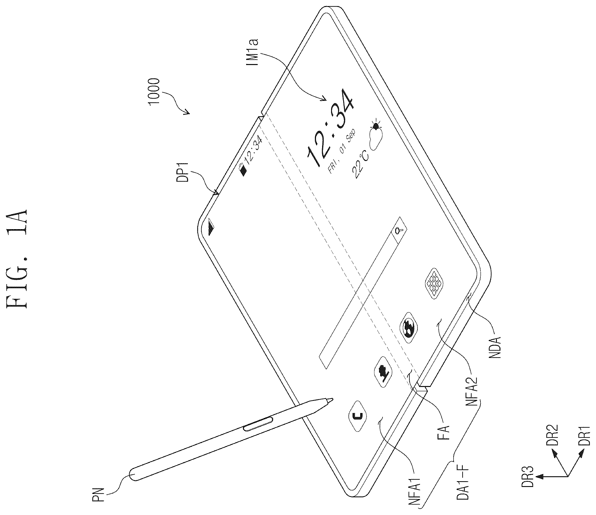
A is a perspective view of an electronic device 1000 , according to some embodiments of the present disclosure. B is a rear perspective view of the electronic device 1000 , according to some embodiments of the present disclosure.
Referring to A and 1 B , the electronic device 1000 may be a device that is configured to be activated based on, or according to, an electrical signal. For example, the electronic device 1000 may be configured to display images and may be configured to sense inputs (e.g., an external input) applied from the outside (e.g., from an external device or object). The external input may be a user input. The user input may include various types of external inputs such as a part of the body of a user (e.g., a user's finger), a pen (or stylus) PN, light, heat, and/or pressure.
The electronic device 1000 may include a first display panel DP 1 and a second display panel DP 2 . The first display panel DP 1 and the second display panel DP 2 may be panels that are separate from each other. For example, as described in more detail below, the first display panel DP 1 and the second display panel DP 2 may be located at opposite sides of the electronic device 1000 . The first display panel DP 1 may be referred to as a “main display panel”. The second display panel DP 2 may be referred to as an “auxiliary display panel” or “external display panel”. According to some embodiments, as described in more detail below, the first display panel DP 1 may be located at a side of the electronic device 1000 that is internal when the electronic device 1000 is in a folded state, such that different non-folding areas of the first display panel DP 1 on opposite sides of a folding area of the first display panel DP 1 face each other in the folded state. According to some embodiments, the second display panel DP 2 may be located at an externally-facing side of the electronic device 1000 when the electronic device 1000 is in the folded state.
The first display panel DP 1 may include a first display unit DA 1 -F (e.g., as shown in A ). The second display panel DP 2 may include a second display unit DA 2 -F (e.g., as shown in B ). An area of the second display panel DP 2 may be smaller than an area of the first display panel DP 1 . The area of the first display unit DA 1 -F may be greater than the area of the second display unit DA 2 -F so as to correspond to the size of the first display panel DP 1 and the size of the second display panel DP 2 .
While the electronic device 1000 is unfolded, the first display unit DA 1 -F may have a plane parallel (or substantially parallel) to a plane defined by the first direction DR 1 and the second direction DR 2 . A thickness direction of the electronic device 1000 may be parallel to a third direction DR 3 intersecting the first direction DR 1 and the second direction DR 2 . Accordingly, front surfaces (or upper surfaces) and back surfaces (or lower surfaces) of members constituting the electronic device 1000 may be defined with respect to the third direction DR 3 .
The first display panel DP 1 or the first display unit DA 1 -F may include a folding area FA, which is configured to be folded and unfolded (e.g., without damaging the electronic device 1000 ), and a plurality of non-folding areas NFA 1 and NFA 2 spaced from each other with the folding area FA therebetween. The second display panel DP 2 may overlap one of the plurality of non-folding areas NFA 1 and NFA 2 . For example, the second display panel DP 2 may overlap the first non-folding area NFA 1 .
A display direction of a first image IM 1 a displayed in a part (e.g., the first non-folding area NFA 1 ) of the first display panel DP 1 may be opposite to a display direction of a second image IM 2 a displayed in the second display panel DP 2 . For example, the first image IM 1 a may be displayed in the third direction DR 3 , and the second image IM 2 a may be displayed in a fourth direction DR 4 , which is the opposite direction to the third direction DR 3 .
According to some embodiments of the present disclosure, the folding area FA may be bent based on (e.g., around) a folding axis extending in a direction (e.g., the second direction DR 2 ) parallel to a long side of the electronic device 1000 . While the electronic device 1000 is folded, the folding area FA has a curvature and radius of curvature (e.g., a set or predetermined curvature and radius of curvature). The first non-folding area NFA 1 and the second non-folding area NFA 2 may face each other, and the electronic device 1000 may be inner-folded such that the first display unit DA 1 -F is not exposed to the outside.
According to some embodiments of the present disclosure, the electronic device 1000 may be outer-folded such that the first display unit DA 1 -F is exposed to the outside. According to some embodiments of the present disclosure, the electronic device 1000 may be capable of both in-folding and out-folding in an unfolded state, but embodiments according to the present disclosure are not limited thereto.
A illustrates that one folding area FA is defined in the electronic device 1000 , but embodiments according to the present disclosure are not limited thereto. For example, a plurality of folding axes and a plurality of folding areas corresponding thereto may be defined in the electronic device 1000 . The electronic device 1000 may be in-folded or out-folded in a state where each of the plurality of folding areas is unfolded.
According to some embodiments of the present disclosure, at least one of the first display panel DP 1 or the second display panel DP 2 may be configured to sense an input by the pen PN even when it does not include a digitizer. Accordingly, because the digitizer for sensing the pen PN may be omitted, an increase in the thickness of the electronic device 1000 , an increase in the weight of the electronic device 1000 , or a decrease in flexibility of the electronic device 1000 may not occur due to the addition of a digitizer. Accordingly, not only the first display panel DP 1 , but also the second display panel DP 2 may be designed to sense the pen PN.
is a perspective view of an electronic device 1000 - 1 , according to some embodiments of the present disclosure.
shows that the electronic device 1000 - 1 is a mobile phone, and the electronic device 1000 - 1 may include a display panel DP.
According to some embodiments of the present disclosure, the display panel DP may be configured to sense inputs applied from the outside (e.g., external input). The external input may be a user input. The user input may include various types of external inputs such as a part of the body of a user (e.g., a user's finger), a pen PN (see A ), light, heat, or pressure.
According to some embodiments of the present disclosure, the display panel DP may be configured to sense an input by the pen PN even though the display panel DP does not include a digitizer. Accordingly, because the digitizer for sensing the pen PN may be omitted, the thickness and weight of the electronic device 1000 - 1 may not increase due to the addition of a digitizer.
A shows a foldable type of the electronic device 1000 , and shows a bar (or non-foldable or flat panel or tablet) type of the electronic device 1000 - 1 . However, embodiments according to the present disclosure described in more detail below are not limited thereto. For example, the descriptions described below may be applied to various electronic devices, such as a rollable type of an electronic device, a slidable type of an electronic device, and a stretchable type of an electronic device.
is a schematic cross-sectional view of the display panel DP, according to some embodiments of the present disclosure.
Referring to , the display panel DP may include a display layer 100 and a sensor layer 200 .
The display layer 100 may be a component that substantially generates or displays images. The display layer 100 may be a light emitting display layer. For example, the display layer 100 may be an organic light emitting display layer, an inorganic light emitting display layer, an organic-inorganic light emitting display layer, a quantum dot display layer, a micro-LED display layer, or a nano-LED display layer. The display layer 100 may include a base layer 110 , a circuit layer 120 , a light emitting element layer 130 , and an encapsulation layer 140 .
The base layer 110 may be a member that provides a base surface on which the circuit layer 120 is located. The base layer 110 may include a multi-layer structure or a single layer structure. The base layer 110 may be a glass substrate, a metal substrate, a silicon substrate, or a polymer substrate, but embodiments according to the present disclosure are not particularly limited thereto.
The circuit layer 120 may be located on the base layer 110 . The circuit layer 120 may include an insulating layer, a semiconductor pattern, a conductive pattern, and a signal line. The insulating layer, the semiconductor layer, and the conductive layer may be formed on the base layer 110 in a manner such as coating, evaporation, or the like. Afterward, the insulating layer, the semiconductor layer, and the conductive layer may be selectively patterned by performing a photolithography process multiple times.
The light emitting element layer 130 may be located on the circuit layer 120 . The light emitting element layer 130 may include a light emitting element. For example, the light emitting element layer 130 may include an organic light emitting material, an inorganic light emitting material, an organic-inorganic light emitting material, a quantum dot, a quantum rod, a micro-LED, or a nano-LED.
The encapsulation layer 140 may be located on the light emitting element layer 130 . The encapsulation layer 140 may protect the light emitting element layer 130 from foreign substances or contaminants such as moisture, oxygen, and dust particles.
The sensor layer 200 may be located on the display layer 100 . The sensor layer 200 may sense an external input applied from the outside. The sensor layer 200 may be an integrated sensor formed continuously during the manufacturing process of the display layer 100 , or may be an external sensor attached to the display layer 100 . In the present disclosure, the sensor layer 200 may be referred to as a sensor, an input sensing layer, an input sensing panel, or an electronic device for sensing input coordinates.
According to some embodiments of the present disclosure, the sensor layer 200 may sense both inputs from a passive-type input source such as the user's body and an input device for generating a magnetic field of a resonant frequency (e.g., a set or predetermined resonant frequency) (e.g., an active-type input source). The input device may be referred to as a “pen”, an “input pen”, a “magnetic pen”, a “stylus pen”, or an “electromagnetic resonance pen”.
is a block diagram for describing an operation of the electronic device 1000 , according to some embodiments of the present disclosure.
Referring to , the display device 1000 may include a display layer 100 , a sensor layer 200 , a display driver 100 C (e.g., a first driver circuit), a sensor driver 200 C (e.g., a second driver circuit), a main driver 1000 C (e.g., a third circuit), and a power supply circuit 1000 P.
The sensor layer 200 may sense a first input 2000 or a second input 3000 applied from the outside (e.g., an external input from an external source). Each of the first input 2000 and the second input 3000 may be an input means or input source capable of providing a change in the capacitance of the sensor layer 200 or an input means capable of causing an induced current in the sensor layer 200 . For example, the first input 2000 may be a passive type of an input method such as a user's body (e.g., a user's finger). The second input 3000 may be an input by the pen PN or an input by an RFIC tag. For example, the pen PN may be a passive-type pen or an active-type pen.
According to some embodiments of the present disclosure, the pen PN may be a device that generates a magnetic field of resonant frequency (e.g., a set or predetermined resonant frequency). The pen PN may be configured to transmit an output signal based on an electromagnetic resonance method. The pen PN may be referred to as an “input device”, an “input pen”, a “magnetic pen”, a “stylus pen”, or an “electromagnetic resonance pen”.
The pen PN may include an RLC resonant circuit, and the RLC resonant circuit may include an inductor L and a capacitor C. According to some embodiments of the present disclosure, the RLC resonant circuit may be a variable resonant circuit that varies a resonance frequency. In this case, the inductor L may be a variable inductor and/or the capacitor C may be a variable capacitor, but embodiments according to the present disclosure are not particularly limited thereto.
The inductor L generates a current by a magnetic field formed in the sensor layer 200 . However, embodiments according to the present disclosure are not particularly limited thereto. For example, when the pen PN operates as an active type of input device, the pen PN may generate a current even when the pen PN does not receive a magnetic field from the outside. The generated current is delivered to the capacitor C. The capacitor C charges the current input from the inductor L, and discharges the charged current to the inductor L. Afterwards, the inductor L may emit a magnetic field at the resonant frequency. An induced current may flow in the sensor layer 200 by the magnetic field emitted by the pen PN, and the induced current may be delivered to the sensor driver 200 C as a reception signal (or a sensing signal).
The main driver 1000 C may control overall operations of the electronic device 1000 . For example, the main driver 1000 C may control operations of the display driver 100 C and the sensor driver 200 C. The main driver 1000 C may include at least one microprocessor and may further include a graphics controller. The main driver 1000 C may be referred to as an “application processor”, “central processing unit”, or “main processor”.
The display driver 100 C may drive the display layer 100 . The display driver 100 C may receive image data and a control signal from the main driver 1000 C. The control signal may include various signals. For example, the control signal may include an input vertical synchronization signal, an input horizontal synchronization signal, a main clock signal, and a data enable signal.
The sensor driver 200 C may drive the sensor layer 200 . The sensor driver 200 C may receive a control signal from the main driver 1000 C. The control signal may include a clock signal of the sensor driver 200 C. Moreover, the control signal may further include a mode determination signal for determining operating modes of the sensor driver 200 C and the sensor layer 200 .
The sensor driver 200 C may be implemented as an integrated circuit (IC) and may be electrically connected to the sensor layer 200 . For example, the sensor driver 200 C may be mounted directly on an area (e.g., a set or predetermined area) of the display panel or mounted on a separate printed circuit board in a chip-on-film (COF) method to be electrically connected to the sensor layer 200 .
The sensor driver 200 C and the sensor layer 200 may selectively operate in a first mode or a second mode. For example, the first mode may be a mode in which a touch input, for example, the first input 2000 is sensed. The second mode may be a mode in which an input of the pen PN, for example, the second input 3000 is sensed. The first mode may be referred to as a “touch sensing mode”, and the second mode may be referred to as a “pen sensing mode”.
The switching between the first mode and the second mode may be accomplished in a variety of manners. For example, the sensor driver 200 C and the sensor layer 200 may be driven in a time-division method in the first mode and the second mode and may sense the first input 2000 and the second input 3000 . Alternatively, the switching between the first mode and the second mode may occur due to a user's selection (e.g., via a user interface) or the user's specific action, either the first mode or the second mode may be activated or deactivated by activating or deactivating a specific application, or one mode may be switched the other mode. Alternatively, while operating alternately in the first mode and the second mode, the sensor driver 200 C and the sensor layer 200 may be maintained in the first mode when the first input 2000 is sensed, or may be maintained in the second mode when the second input 3000 is sensed.
The sensor driver 200 C may calculate coordinate information of an input based on a signal received from the sensor layer 200 and may provide the main driver 1000 C with a coordinate signal having the coordinate information. The main driver 1000 C executes an operation corresponding to a user input based on the coordinate signal. For example, the main driver 1000 C may operate the display driver 100 C such that a new application image is displayed on the display layer 100 .
The power supply circuit 1000 P may include a power management integrated circuit (PMIC). The power supply circuit 1000 P may generate a plurality of driving voltages for driving the display layer 100 , the sensor layer 200 , the display driver 100 C, and the sensor driver 200 C. For example, the plurality of driving voltages may include a gate high voltage, a gate low voltage, a first driving voltage (e.g., ELVSS voltage), a second driving voltage (e.g., ELVDD voltage), an initialization voltage, and the like, but embodiments according to the present disclosure are not particularly limited thereto.
is a cross-sectional view of the display panel DP, according to some embodiments of the present disclosure.
Referring to , at least one buffer layer BFL is formed on an upper surface of a base layer 110 . The buffer layer BFL may improve a bonding force between the base layer 110 and a semiconductor pattern. The buffer layer BFL may be formed of multiple layers. Alternatively, the display layer 100 may further include a barrier layer. The buffer layer BFL may include at least one of silicon oxide, silicon nitride, or silicon oxynitride. For example, the buffer layer BFL may include a structure in which a silicon oxide layer and a silicon nitride layer are stacked alternately.
The semiconductor patterns SC, AL, DR, and SCL may be located on the buffer layer BFL. The semiconductor patterns SC, AL, DR, and SCL may include polysilicon. However, embodiments according to the present disclosure are not limited thereto. For example, the semiconductor patterns SC, AL, DR, and SCL may include amorphous silicon, low-temperature polycrystalline silicon, or an oxide semiconductor.
only illustrates a part of the semiconductor patterns SC, AL, DR, and SCL, and the semiconductor pattern may be further located in another area. The semiconductor patterns SC, AL, DR, and SCL may be arranged across pixels in a specific rule. The semiconductor patterns SC, AL, DR, and SCL may have different electrical properties depending on whether the semiconductor patterns SC, AL, DR, and SCL are doped. The semiconductor patterns SC, AL, DR, and SCL may include the first areas SC, DR, and SCL having a high conductivity, and the second area AL having a low conductivity. The first areas SC, DR, and SCL may be doped with an N-type dopant or a P-type dopant. A P-type transistor may include an area doped with the P-type dopant, and an N-type transistor may include an area doped with the N-type dopant. The second area AL may be an undoped area or an area doped with a concentration lower than a concentration in the first area SC, DR, and SCL.
A conductivity of each of the first areas SC, DR, and SCL is greater than a conductivity of the second area AL. The first areas SC, DR, and SCL may substantially serves as an electrode or a signal line. The second area AL may actually correspond to an active area AL (or a channel) of a transistor 100 PC. In other words, a portion AL of the semiconductor patterns SC, AL, DR, and SCL may be the active area AL of a transistor 100 PC; other parts SC and DR may be the source area SC or the drain area DR of the transistor 100 PC; and the other part SCL may be a connection electrode or a connection signal line SCL.
Each of pixels may be expressed by an equivalent circuit including 7 transistors, one capacitor, and a light emitting element, and the equivalent circuit of the pixel may be modified in various forms, and the circuit of the pixel may include additional components or fewer components without departing from the spirit and scope of embodiments according to the present disclosure. One transistor 100 PC and the one light emitting element 100 PE included in a pixel are illustrated in by way of example.
The source area SC, the active area AL, and the drain area DR of the transistor 100 PC may be formed from the semiconductor patterns SC, AL, DR, and SCL. The source area SC and the drain area DR may extend in directions opposite to each other from the active area AL in a cross-sectional view. A portion of the connection signal line SCL formed from the semiconductor patterns SC, AL, DR, and SCL is illustrated in . According to some embodiments, the connection signal line SCL may be connected to the drain area DR of the transistor 100 PC in a plan view.
A first insulating layer 10 may be located on the buffer layer BFL. The first insulating layer 10 may overlap a plurality of pixels in common and may cover the semiconductor patterns SC, AL, DR, and SCL. The first insulating layer 10 may be an inorganic layer and/or an organic layer, and may have a single layer or multi-layer structure. The first insulating layer 10 may include at least one of aluminum oxide, titanium oxide, silicon oxide, silicon nitride, silicon oxynitride, zirconium oxide, or hafnium oxide. According to some embodiments, the first insulating layer 10 may be a silicon oxide layer having a single layer structure. Not only the first insulating layer 10 but also an insulating layer of the circuit layer 120 to be described in more detail later may be an inorganic layer and/or an organic layer, and may have a single layer structure or a multi-layer structure. The inorganic layer may include at least one of the above-described materials, but embodiments according to the present disclosure are not limited thereto.
A gate GT of the transistor 100 PC is located on the first insulating layer 10 . The gate GT may be a part of a metal pattern. The gate GT overlaps the active area AL. The gate GT may function as a mask in a process of reducing the semiconductor patterns SC, AL, DR, and SCL.
A second insulating layer 20 is located on the first insulating layer 10 and may cover the gate GT. The second insulating layer 20 may overlap a plurality of pixels in common. The second insulating layer 20 may be an inorganic layer and/or an organic layer, and may have a single layer structure or a multi-layer structure. The second insulating layer 20 may include at least one of silicon oxide, silicon nitride, or silicon oxynitride. According to some embodiments, the second insulating layer 20 may have a multi-layer structure including a silicon oxide layer and a silicon nitride layer.
A third insulating layer 30 may be located on the second insulating layer 20 . The third insulating layer 30 may have a single layer structure or a multi-layer structure. For example, the third insulating layer 30 may have a multi-layer structure including a silicon oxide layer and a silicon nitride layer.
A first connection electrode CNE 1 may be located on the third insulating layer 30 . The first connection electrode CNE 1 may be connected to the connection signal line SCL through a contact hole CNT-1 penetrating through the first, second, and third insulating layers 10 , 20 , and 30 .
A fourth insulating layer 40 may be located on the third insulating layer 30 . The fourth insulating layer 40 may be a single silicon oxide layer. A fifth insulating layer 50 may be located on the fourth insulating layer 40 . The fifth insulating layer 50 may be an organic layer.
A second connection electrode CNE 2 may be located on the fifth insulating layer 50 . The second connection electrode CNE 2 may be connected to the first connection electrode CNE 1 through a contact hole CNT-2 passing through the fourth insulating layer 40 and the fifth insulating layer 50 .
A sixth insulating layer 60 may be located on the fifth insulating layer 50 and may cover the second connection electrode CNE 2 . The sixth insulating layer 60 may be an organic layer.
The light emitting element layer 130 may be located on the circuit layer 120 . The light emitting element layer 130 may include a light emitting element 100 PE. For example, the light emitting element layer 130 may include an organic light emitting material, an inorganic light emitting material, an organic-inorganic light emitting material, a quantum dot, a quantum rod, a micro-LED, or a nano-LED. Hereinafter, the description will be given in the context of the light emitting element 100 PE being an organic light emitting element, but embodiments according to the present disclosure are limited thereto.
The light emitting element 100 PE may include a first electrode AE, a light emitting layer EL, and a second electrode CE.
The first electrode AE may be located on the sixth insulating layer 60 . The first electrode AE may be connected to the second connection electrode CNE 2 through a contact hole CNT-3 penetrating through the sixth insulating layer 60 .
A pixel defining layer 70 may be located on the sixth insulating layer 60 and may cover a portion of the first electrode AE. An opening 70 -OP is defined in the pixel defining layer 70 . The opening 70 -OP of the pixel defining layer 70 exposes at least a portion of the first electrode AE.
The active area 1000 A (see A ) may include an emission area PXA and a non-emission area NPXA adjacent to the emission area PXA. The non-emission area NPXA may surround (e.g., in a periphery or outside a footprint of) the emission area PXA. According to some embodiments, the emission area PXA is defined to correspond to a partial area of the first electrode AE, which is exposed by the opening 70 -OP. For example, according to some embodiments, the first electrode AE may be located within the emission area PXA and may extend into the non-emission area NPXA in a plan view.
The light emitting layer EL may be located on the first electrode AE. The light emitting layer EL may be located in an area corresponding to the opening 70 -OP. That is, the light emitting layer EL may be separately formed on each of pixels. When the light emitting layers EL are separately formed in each of pixels, each of the light emitting layers EL may emit light of at least one of a blue color, a red color, or a green color. However, embodiments according to the present disclosure are not limited thereto. For example, the light emitting layer EL may be included in a plurality of pixels in common while having an integral shape. In this case, the light emitting layer EL may provide blue light or white light.
The second electrode CE may be located on the light emitting layer EL. The second electrode CE may be included in a plurality of pixels in common while having an integral shape.
According to some embodiments of the present disclosure, a hole control layer may be interposed between the first electrode AE and the light emitting layer EL. The hole control layer may be arranged in common in the emission area PXA and the non-emission area NPXA. The hole control layer may include a hole transport layer and may further include a hole injection layer. An electron control layer may be interposed between the light emitting layer EL and the second electrode CE. The electron control layer may include an electron transport layer, and may further include an electron injection layer. The hole control layer and the electron control layer may be formed in common in a plurality of pixels by using an open mask or inkjet process.
The encapsulation layer 140 may be located on the light emitting element layer 130 . The encapsulation layer 140 may include an inorganic layer, an organic layer, and an inorganic layer sequentially stacked, and layers constituting the encapsulation layer 140 are not limited thereto. The inorganic layers may protect the light emitting element layer 130 from impurities or contaminants such as moisture and oxygen, and the organic layer may protect the light emitting element layer 130 from a foreign material or contaminants such as dust particles. The inorganic layers may include a silicon nitride layer, a silicon oxynitride layer, a silicon oxide layer, a titanium oxide layer, an aluminum oxide layer, or the like. The organic layer may include, but is not limited to, an acrylic-based organic layer.
The sensor layer 200 may include a base layer 201 , a first conductive layer 202 , an intermediate insulating layer 203 , a second conductive layer 204 , and a cover insulating layer 205 .
The base layer 201 may be an inorganic layer including at least one of silicon nitride, silicon oxynitride, or silicon oxide. Alternatively, the base layer 201 may be an organic layer including an epoxy resin, an acrylate resin, or an imide-based resin. The base layer 201 may have a single layer structure or may have a multi-layer structure stacked in the third direction DR 3 .
Each of the first conductive layer 202 and the second conductive layer 204 may have a single layer structure or may have a multi-layer structure in which layers are stacked in the third direction DR 3 .
Each of the first conductive layer 202 and the second conductive layer 204 of a single layer structure may include a metal layer or a transparent conductive layer. The metal layer may include molybdenum, silver, titanium, copper, aluminum, or an alloy thereof. The transparent conductive layer may include a transparent conductive oxide such as indium tin oxide (ITO), indium zinc oxide (IZO), zinc oxide (ZnO), indium zinc tin oxide (IZTO), or the like. Besides, the transparent conductive layer may include a conductive polymer such as poly(3,4-ethylenedioxythiophene) (PEDOT), a metal nano wire, graphene, and the like.
Each of the first conductive layer 202 and the second conductive layer 204 of the multi-layer structure may include metal layers. For example, the metal layers may have a three-layer structure of titanium/aluminum/titanium. The conductive layer of the multi-layer structure may include at least one metal layer and at least one transparent conductive layer.
At least one of the intermediate insulating layer 203 or the cover insulating layer 205 may include an inorganic film. The inorganic film may include at least one of aluminum oxide, titanium oxide, silicon oxide, silicon nitride, silicon oxynitride, zirconium oxide, or hafnium oxide.
At least one of the intermediate insulating layer 203 or the cover insulating layer 205 may include an organic film. The organic film may include at least one of acrylate-based resin, methacrylate-based resin, polyisoprene, vinyl-based resin, epoxy-based resin, urethane-based resin, cellulose-based resin, siloxane-based resin, polyimide-based resin, polyamide-based resin, or perylene-based resin.
is a plan view of the sensor layer 200 , according to some embodiments of the present disclosure. is an enlarged plan view of one sensing unit SU, according to some embodiments of the present disclosure. A is a plan view showing a first conductive layer 202 SU of the sensing unit SU, according to some embodiments of the present disclosure. B is a plan view showing a second conductive layer 204 SU of the sensing unit SU, according to some embodiments of the present disclosure. is a cross-sectional view of the sensor layer 200 taken along line I-I′ shown in A and 8 B , according to some embodiments of the present disclosure.
Referring to , a sensing area 200 A and a peripheral area (or peripheral region) 200 NA adjacent to (e.g., in a periphery or outside a footprint of) the sensing area 200 A may be defined in the sensor layer 200 .
The sensor layer 200 may include a plurality of first electrodes 210 , a plurality of second electrodes 220 , a plurality of third electrodes 230 , and a plurality of fourth electrodes 240 , which are located in the sensing area 200 A. The first electrodes 210 may be referred to as first sensing electrodes, the second electrodes 220 may be referred to as second sensing electrodes, the third electrodes 230 may be referred to as first electrodes, and the fourth electrodes 240 may be referred to as second electrodes.
The first electrodes 210 , the second electrodes 220 , the third electrodes 230 , and the fourth electrodes 240 may correspond to a main region, between first and second peripheral regions on opposite sides (e.g., the left and right sides in ). Thus, the main region of the sensor layer 200 may be located between a first peripheral region (e.g., the left side of the peripheral area 200 NA) and a second peripheral region (e.g., the right side of the peripheral area 200 NA). The main region of the sensor layer 200 may be the sensing area 200 A.
The first electrodes 210 may intersect the second electrodes 220 . Each of the first electrodes 210 may extend in the second direction DR 2 . The first electrodes 210 may be arranged to be spaced apart from each other in the first direction DR 1 . Each of the second electrodes 220 may extend in the first direction DR 1 . The second electrodes 220 may be arranged to be spaced apart from each other in the second direction DR 2 . The sensing unit SU of the sensor layer 200 may be an area where the one first electrode 210 intersects the one second electrode 220 .
illustrates the six first electrodes 210 and the ten second electrodes 220 , and illustrates the 60 sensing units SU. However, the number of first electrodes 210 and the number of second electrodes 220 are not limited thereto.
Referring to , each of the first electrodes 210 may include first division electrodes 210 dv 1 and 210 dv 2 . The first division electrodes 210 dv 1 and 210 dv 2 may extend in the second direction DR 2 and may be spaced apart from each other in the first direction DR 1 . The first division electrodes 210 dv 1 and 210 dv 2 may have a line-symmetrical shape with respect to a line extending in the second direction DR 2 .
Each of the second electrodes 220 may include second division electrodes 220 dv 1 and 220 dv 2 . The second electrodes 220 extend in the first direction DR 1 and may be spaced from each other in the second direction DR 2 . The second division electrodes 220 dv 1 and 220 dv 2 may have a line-symmetrical shape with respect to a line extending in the first direction DR 1 .
Referring to , 8 A, 8 B, and 9 , each of the second division electrodes 220 dv 1 and 220 dv 2 may include a sensing pattern 221 and a bridge pattern 222 . The sensing pattern 221 and the bridge pattern 222 may be located or formed on different layers, and the sensing pattern 221 and the bridge pattern 222 may be electrically connected to each other through a first contact CNa. For example, the bridge pattern 222 may be included in a first conductive layer 202 SU. The sensing pattern 221 and the first division electrodes 210 dv 1 and 210 dv 2 may be included in a second conductive layer 204 SU. The first conductive layer 202 SU may be included in the first conductive layer 202 of , and the second conductive layer 204 SU may be included in the second conductive layer 204 of .
Each of the third electrodes 230 may extend in the second direction DR 2 . The third electrodes 230 may be arranged to be spaced apart from each other in the first direction DR 1 . According to some embodiments of the present disclosure, each of the third electrodes 230 may include a plurality of first auxiliary electrodes 230 s that are electrically connected in parallel. The number of first auxiliary electrodes 230 s included in each of the third electrodes 230 may be varied. For example, as the number of first auxiliary electrodes 230 s included in each of the third electrodes 230 increases, the resistance of each of the third electrodes 230 may be lowered. Accordingly, power efficiency may be relatively improved and sensing sensitivity may be relatively improved. On the other hand, as the number of first auxiliary electrodes 230 s included in each of the third electrodes 230 decreases, the loop coil pattern formed by using the third electrodes 230 may be implemented in diverse forms.
illustrates that the one third electrode 230 includes the two first auxiliary electrodes 230 s , but embodiments according to the present disclosure are not particularly limited thereto. The first auxiliary electrodes 230 s may be arranged in a one-to-one correspondence with the first electrodes 210 . Accordingly, the one sensing unit SU may include a portion of the one first auxiliary electrode 230 s.
A coupling capacitor may be defined between the one first electrode 210 and the one first auxiliary electrode 230 s . In this case, the current induced when a pen is sensed may be delivered from the first auxiliary electrode 230 s to the first electrode 210 through the coupling capacitor. In other words, the first auxiliary electrode 230 s may compensate for a signal delivered from the first electrode 210 to the sensor driver 200 C. Accordingly, the greatest effect may be achieved when a phase of the signal induced in the first auxiliary electrode 230 s matches a phase of the signal induced in the first electrode 210 . Therefore, the center of each of the first electrodes 210 in the first direction DR 1 may overlap the center of each of the first auxiliary electrodes 230 s in the first direction DR 1 .
According to some embodiments of the present disclosure, because the one third electrode 230 includes the two first auxiliary electrodes 230 s , the one third electrode 230 may correspond to (or overlap) the two first electrodes 210 . Accordingly, the number of first electrodes 210 included in the sensor layer 200 may be greater than the number of third electrodes 230 . For example, the number of first electrodes 210 may be equal to the product of the number of third electrodes 230 included in the sensor layer 200 and the number of first auxiliary electrodes 230 s included in each of the third electrodes 230 . In , the number of first electrodes 210 may be 6; the number of third electrodes 230 may be 3; and the number of first auxiliary electrodes 230 s included in each of the third electrodes 230 may be 2, although embodiments according to the present disclosure are not limited thereto, and the number of first, third, and first auxiliary electrodes may vary according to various embodiments.
The fourth electrodes 240 may be arranged in the second direction DR 2 , and the fourth electrodes 240 may extend in the first direction DR 1 . According to some embodiments of the present disclosure, each of the fourth electrodes 240 may include second auxiliary electrodes 240 s 1 or 240 s 2 electrically connected to each other. The second auxiliary electrodes 240 s 1 or 240 s 2 may be referred to as the 2-1st auxiliary electrode 240 s 1 and the 2-2nd auxiliary electrode 240 s 2 .
Routing directions of the second auxiliary electrode 240 s 1 and the second auxiliary electrode 240 s 2 may be different from each other. illustrates the two fourth electrodes 240 and the five second auxiliary electrodes 240 s 1 or 240 s 2 included in each of the fourth electrodes 240 .
In this specification, the fact that the routing directions are different from each other means that connection locations of electrodes and trace lines are different from each other. For example, a first connection location of a fourth trace line 240 t - 1 electrically connected to the second auxiliary electrode 240 s 1 may be different from a second connection location of a fourth trace line 240 t - 2 electrically connected to the second auxiliary electrode 240 s 2 . The first connection location may be placed at a left end based on the second auxiliary electrode 240 s 1 . The second connection location may be placed at a right end of the second auxiliary electrode 240 s 2 .
shows that the five second auxiliary electrodes 240 s 1 are electrically connected to each other, and the five second auxiliary electrodes 240 s 2 are electrically connected to each other. That is, the area ratio of the two fourth electrodes 240 or the number ratio of the second auxiliary electrode included in each of the two fourth electrodes 240 may have a ratio of 1:1. However, embodiments according to the present disclosure are not particularly limited thereto. For example, according to some embodiments, the number of second auxiliary electrodes 240 s 1 may be different from the number of second auxiliary electrodes 240 s 2 .
According to some embodiments of the present disclosure, when each of the fourth electrodes 240 includes the second auxiliary electrodes 240 s 1 or 240 s 2 connected in parallel, the area of one fourth electrode may be increased. Furthermore, as the resistance of each of the fourth electrodes 240 is lowered, the sensing sensitivity for the second input 3000 (see ) may be relatively improved.
A coupling capacitor may be defined between the one second electrode 220 and the one second auxiliary electrode 240 s 1 . In this case, the current induced when a pen is sensed may be delivered from the second auxiliary electrode 240 s 1 to the second electrode 220 through the coupling capacitor. In other words, the second auxiliary electrode 240 s 1 may compensate for a signal delivered from the second electrode 220 to the sensor driver 200 C. Accordingly, the greatest effect may be achieved when a phase of the signal induced in the second auxiliary electrode 240 s 1 matches a phase of the signal induced in the second electrode 220 . Therefore, the center of each of the first electrodes 220 in the second direction DR 2 may overlap the center of each of the second auxiliary electrodes 240 s 1 in the second direction DR 2 .
Referring to , 8 A, and 8 B , each of the first auxiliary electrodes 230 s included in the third electrode 230 may include a 3-1st pattern 231 and a 3-2nd pattern 232 . The 3-1st pattern 231 and the 3-2nd pattern 232 may be placed on different layers. The 3-1st pattern 231 and the 3-2nd pattern 232 may be electrically connected to each other through a second contact CNb. The 3-1st pattern 231 may be included in the first conductive layer 202 SU. The 3-2nd pattern 232 may be included in the second conductive layer 204 SU.
According to some embodiments of the present disclosure, a part of the 3-1st pattern 231 may overlap a part of each of the first division electrodes 210 dv 1 and 210 dv 2 . Accordingly, coupling capacitance may be provided (or formed) between the first electrode 210 and the third electrode 230 .
Referring to , 8 A, and 8 B , the second auxiliary electrodes 240 s 1 or 240 s 2 included in the fourth electrode 240 may include a 4-1st pattern 241 , a 4-2nd pattern 242 , and a 4-3rd pattern 243 . The 4-2nd pattern 242 and the 4-3rd pattern 243 may be placed on the same layer as each other. The 4-1st pattern 241 may be placed on a different layer from the 4-2nd pattern 242 and the 4-3rd pattern 243 . The 4-1st pattern 241 and the 4-2nd pattern 242 may be electrically connected to each other through a third contact CNc. The 4-1st pattern 241 and the 4-3rd pattern 243 may be electrically connected to each other through a fourth contact CNd. The 4-2nd pattern 242 , and the 4-3rd pattern 243 may be included in the first conductive layer 202 SU, and the 4-1st pattern 241 may be included in the second conductive layer 204 SU.
According to some embodiments of the present disclosure, a part of the 4-2nd pattern 242 may overlap the sensing pattern 221 of each of the second division electrodes 220 dv 1 and 220 dv 2 . Accordingly, coupling capacitor may be defined (or provided/formed) between the second electrode 220 and the fourth electrode 240 .
According to some embodiments of the present disclosure, the first conductive layer 202 SU may further include dummy patterns DMP. Each of the dummy patterns DMP may be electrically floated or electrically grounded. According to some embodiments of the present disclosure, the dummy patterns DMP may be omitted. Alternatively, the dummy patterns DMP may be electrically connected to the first electrode 210 or the second electrode 220 .
The sensor layer 200 may further include a plurality of second trace lines 210 t placed in the peripheral area 200 NA, the plurality of first pads PD 1 connected to the first trace lines 210 t in a one-to-one correspondence, a plurality of second trace lines 220 t , and a plurality of second pads PD 2 connected to the second trace lines 220 t in a one-to-one correspondence.
The first trace lines 210 t may be electrically connected to the first electrodes 210 in a one-to-one correspondence. The two first division electrodes 210 dv 1 and 210 dv 2 included in the one first electrode 210 may be connected to one of the first trace lines 210 t . Each of the first trace lines 210 t may include a plurality of branch units to be connected to the two first division electrodes 210 dv 1 and 210 dv 2 . According to some embodiments of the present disclosure, the two first division electrodes 210 dv 1 and 210 dv 2 may be connected to each other within the sensing area 200 A.
The second trace lines 220 t may be electrically connected to the second electrodes 220 in a one-to-one correspondence. The two second division electrodes 220 dv 1 and 220 dv 2 included in the one second electrode 220 may be connected to one of the second trace lines 220 t . Each of the second trace lines 220 t may include a plurality of branch units to be connected to the two second division electrodes 220 dv 1 and 220 dv 2 . According to some embodiments of the present disclosure, the two second division electrodes 220 dv 1 and 220 dv 2 may be connected to each other within the sensing area 200 A.
According to some embodiments of the present disclosure, the second electrodes 220 may be classified into (or divided into) a first electrode group 220 G 1 and a second electrode group 220 G 2 . The first electrode group 220 G 1 and the second electrode group 220 G 2 may be adjacent in the second direction DR 2 . Some second electrodes 220 - 1 (hereinafter referred to as “2-1st electrodes”) among the second electrodes 220 may be included in the first electrode group 220 G 1 , and some second electrodes 220 - 2 (hereinafter referred to as “2-2nd electrodes”) of the remaining second electrodes 220 - 2 among the second electrodes 220 may be included in the second electrode group 220 G 2 .
A boundary RIL may be defined between the first electrode group 220 G 1 and the second electrode group 220 G 2 . Accordingly, the 2-1st electrodes 220 - 1 and the 2-2nd electrodes 220 - 2 may be spaced apart from each other with the boundary RIL therebetween. A routing direction of each of the 2-1st electrodes 220 - 1 may be different from a routing direction of each of the 2-2nd electrodes 220 - 2 .
The second trace lines 220 t may be classified into a first trace group 220 t G 1 electrically connected to the first electrode group 220 G 1 and a second trace group 220 t G 2 electrically connected to the second electrode group 220 G 2 . The first trace group 220 t G 1 and the second trace group 220 t G 2 may be spaced apart from each other with the sensing area 200 A therebetween.
The sensor layer 200 may further include a third trace line 230 rt 1 placed in the peripheral area 200 NA, a plurality of third pads PD 3 connected to one end and the other end of the third trace line 230 rt 1 , fourth trace lines 240 t - 1 and 240 t - 2 , fourth pads PD 4 connected to the fourth trace lines 240 t - 1 and 240 t - 2 in a one-to-one correspondence, fifth trace lines 230 rt 2 , and a fifth pad PD 5 connected to the fifth trace lines 230 rt 2 in a one-to-one correspondence.
The third trace line 230 rt 1 may be electrically connected to all of the third electrodes 230 . The third trace line 230 rt 1 may include a first line portion 231 t extending in the first direction DR 1 and electrically connected to the third electrodes 230 , a second line portion 232 t extending from a first end of the first line portion 231 t in the second direction DR 2 , and a third line portion 233 t extending from a second end of the first line portion 231 t in the second direction DR 2 .
According to some embodiments of the present disclosure, each of the resistance of the second line portion 232 t and the resistance of the third line portion 233 t may be substantially the same as the resistance of a third electrode of one of the third electrodes 230 . Accordingly, the second line portion 232 t and the third line portion 233 t may serve as the third electrodes 230 , and the same effect that the third electrodes 230 are also placed in the peripheral area 200 NA may be obtained. For example, one of the second line portion 232 t and the third line portion 233 t and one of the third electrodes 230 may form a coil. Accordingly, a pen located in an area adjacent to the peripheral area 200 NA may also be sufficiently charged by a loop including the second line portion 232 t or the third line portion 233 t.
According to some embodiments of the present disclosure, to adjust the resistance of each of the second line portion 232 t and the third line portion 233 t , the width of each of the second line portion 232 t and the third line portion 233 t in the first direction DR 1 may be adjusted. However, this is only an example, and the first to third line portions 231 t , 232 t , and 233 t may have the same (or substantially the same) width as each other.
The fifth trace lines 230 rt 2 may be connected to the third electrodes 230 in a one-to-one correspondence. In other words, the number of fifth trace lines 230 rt 2 may correspond to the number of third electrodes 230 . In , the three fifth trace lines 230 rt 2 are shown.
According to some embodiments of the present disclosure, the fifth trace lines 230 rt 2 and the fifth pad PD 5 may be omitted, and a charging driving mode for charging a pen may be omitted. In this case, the sensor layer 200 may sense an input from an active-type pen capable of emitting a magnetic field even when a magnetic field is not provided from the sensor layer 200 .
According to some embodiments of the present disclosure, the fourth electrodes 240 may include one fourth electrode 240 G 1 (hereinafter referred to as a “4-1st electrode”) overlapping the first electrode group 220 G 1 and the other fourth electrode 240 G 2 (hereinafter referred to as a “4-2nd electrode”) overlapping the second electrode group 220 G 2 . The 4-1st electrode 240 G 1 may include a 2-1st auxiliary electrodes 240 s 1 . The 4-2nd electrode 240 G 2 may include a 2-2nd auxiliary electrodes 240 s 2 .
The fourth trace lines 240 t - 1 and 240 t - 2 may be spaced apart from each other with the sensing area 200 A therebetween. The fourth trace line 240 t - 1 (hereinafter referred to as a “4-1st trace line”) among the fourth trace lines 240 t - 1 and 240 t - 2 may be electrically connected to the 4-1st electrode 240 G 1 . The other fourth trace line 240 t - 2 (hereinafter referred to as a “4-2nd trace line”) among the fourth trace lines 240 t - 1 and 240 t - 2 may be electrically connected to the 4-2nd electrode 240 G 2 . One end of each of the 2-1st auxiliary electrodes 240 s 1 may be connected to the 4-1st trace line 240 t - 1 . One end of each of the 2-2nd auxiliary electrodes 240 s 2 may be connected to the 4-2nd trace line 240 t - 2 .
The 4-1st trace line 240 t - 1 and the 4-2nd trace line 240 t - 2 may be spaced apart from each other with the sensing area 200 A therebetween. The 4-1st trace line 240 t - 1 and the first trace group 220 t G 1 may be spaced apart from each other with the sensing area 200 A therebetween. Furthermore, the 4-2nd trace line 240 t - 2 and the second trace group 220 t G 2 may be spaced apart from each other with the sensing area 200 A therebetween. The second trace group 220 t G 2 and the 4-1st trace line 240 t - 1 may be placed in one portion of the peripheral area 200 NA placed on the left side of the sensing area 200 A. The first trace group 220 t G 1 and the 4-2nd trace line 240 t - 2 may be placed in one portion of the peripheral area 200 NA placed on the right side of the sensing area 200 A.
A is an enlarged plan view of the area AA′ shown in A . B is an enlarged plan view of the area BB′ shown in B .
Referring to A, 8 B, 10 A, and 10 B , each of the first electrodes 210 , the second electrodes 220 , the third electrodes 230 , the fourth electrodes 240 , and the dummy patterns DMP may have a mesh structure. Each of the mesh structures may include a plurality of mesh lines. Each of the plurality of mesh lines may have a shape extending in a direction (e.g., a set or predetermined direction) and may be connected to each other. The shape may have various shapes such as a straight line, a line with protrusions, or an uneven line. Openings in which no mesh structure is located may be defined (provided or formed) in each of the first electrodes 210 , the second electrodes 220 , the third electrodes 230 , the fourth electrodes 240 , and the dummy patterns DMP.
A and 10 B illustrate that the mesh structure includes mesh lines extending in a first cross direction CDR 1 intersecting the first direction DR 1 and the second direction DR 2 , and mesh lines extending in the second cross direction CDR 2 intersecting the first cross direction CDR 1 . However, the extension direction of the mesh lines constituting the mesh structure is not particularly limited to the illustrations in A and 10 B . For example, the mesh structure may include only mesh lines extending in the first direction DR 1 and the second direction DR 2 , or may include mesh lines extending in the first direction DR 1 , the second direction DR 2 , and the first cross direction CDR 1 , and the second cross direction CDR 2 . In other words, the mesh structure may be changed into various forms.
is a diagram showing an operation of a sensor driver 200 C (see ), according to some embodiments of the present disclosure.
Referring to , the sensor driver 200 C may be configured to selectively operate in one of a first operating mode DMD 1 , a second operating mode DMD 2 , or a third operating mode DMD 3 .
The first operating mode DMD 1 may be referred to as a “touch and pen standby mode”; the second operating mode DMD 2 may be referred to as a “touch activation and pen standby mode”; and, the third operating mode DMD 3 may be referred to as a “pen activation mode”. The first operating mode DMD 1 may be in a mode for waiting for the first input 2000 and the second input 3000 . The second operating mode DMD 2 may be in a mode for sensing the first input 2000 and waiting for the second input 3000 . The third operating mode DMD 3 may be a mode for sensing the second input 3000 .
According to some embodiments of the present disclosure, the sensor driver 200 C may be driven first in the first operating mode DMD 1 . When the first input 2000 is sensed in the first operating mode DMD 1 , the sensor driver 200 C may be switched (or changed) to the second operating mode DMD 2 . Alternatively, when the second input 3000 is sensed in the first operating mode DMD 1 , the sensor driver 200 C may be switched (or changed) to the third operating mode DMD 3 .
According to some embodiments of the present disclosure, when the second input 3000 is sensed in the second operating mode DMD 2 , an operating mode of the sensor driver 200 C may be switched to the third operating mode DMD 3 . When the first input 2000 is terminated (or not detected) in the second operating mode DMD 2 , an operating mode of the sensor driver 200 C may be switched to the first operating mode DMD 1 . When the second input 3000 is terminated (or not detected) in the third operating mode DMD 3 , an operating mode of the sensor driver 200 C may be switched to the first operating mode DMD 1 .
A is a diagram showing an operation of a sensor driver 200 C (see ), according to some embodiments of the present disclosure.
Referring to , 11 , and 12 A , operations in the first to third operating modes DMD 1 , DMD 2 , and DMD 3 are shown in order of time (t).
In the first operating mode DMD 1 , the sensor driver 200 C may be repeatedly driven in a second mode MD 2 - d and a first mode MD 1 - d . During the second mode MD 2 - d , the sensor layer 200 may perform a scan driving operation to detect the second input 3000 . During the first mode MD 1 - d , the sensor layer 200 may perform a scan driving operation to detect the first input 2000 . A illustrates that the sensor driver 200 C operates in the first mode MD 1 - d continuously after the second mode MD 2 - d , but the order is not limited thereto.
In the second operating mode DMD 2 , the sensor driver 200 C may be repeatedly driven in a second mode MD 2 - d and a first mode MD 1 . During the second mode MD 2 - d , the sensor layer 200 may perform a scan driving operation to detect the second input 3000 . During the first mode MD 1 , the sensor layer 200 may perform a scan driving operation to detect coordinates by the first input 2000 .
In the third operating mode DMD 3 , the sensor driver 200 C may be driven in a second mode MD 2 . During the second mode MD 2 , the sensor layer 200 may perform a scan driving operation to detect coordinates by the second input 3000 . In the third operating mode DMD 3 , the sensor driver 200 C may not operate in the first mode MD 1 - d or MD 1 until the second input 3000 is terminated (or not detected).
Referring to together, in the first mode MD 1 - d and the first mode MD 1 , all of the third electrodes 230 and the fourth electrodes 240 may be grounded. Accordingly, touch noise entering through the third electrodes 230 and the fourth electrodes 240 may be prevented or reduced.
In the second mode MD 2 - d and the second mode MD 2 , one end of each of the third electrodes 230 and the fourth electrodes 240 may be floated. Moreover, in the second mode MD 2 - d and the second mode MD 2 , the other end of each of the third electrodes 230 and the fourth electrodes 240 may be grounded or floated. Accordingly, compensation of the sensing signal may be maximized or improved by the coupling between the first electrodes 210 and the third electrodes 230 and the coupling between the second electrodes 220 and the fourth electrodes 240 .
B is a diagram showing an operation of the second mode MD 2 , according to some embodiments of the present disclosure.
Referring to B , the second mode MD 2 may include a first driving mode MD 2 - 1 and a second driving mode MD 2 - 2 . The first driving mode MD 2 - 1 of the second mode MD 2 may be referred to as a “proactive driving mode”, and the second driving mode MD 2 - 2 of the second driving mode MD 2 may be referred to as a “main driving mode”
The first driving mode MD 2 - 1 may include a touch driving mode FT, a charging driving mode SCC, and a pre-pen sensing driving mode PSS. The second driving mode MD 2 - 2 may include the touch driving mode FT, the charging driving mode SCC, and a pen sensing driving mode SS.
The touch driving mode FT may be a mode driven to detect touches by a palm or a blade of a hand. However, only a touch is detected, and an operation corresponding to an input may not be executed. In other words, the touch driving mode FT may only detect that a touch of a palm or a blade of a hand is occurring, and may be a mode in which coordinates are recognized and an operation corresponding to the recognized result is not executed. In other words, according to some embodiments, during the touch driving mode FT, whether or not a touch occurs may be detected or determined, without regard for the location or coordinates of the touch. According to some embodiments of the present disclosure, the touch driving mode FT may be omitted in at least one of the first driving mode MD 2 - 1 or the second driving mode MD 2 - 2 .
The charging driving mode SCC may be a mode in which a signal for charging a pen is provided. In the charging driving mode SCC, a magnetic field may be formed in the sensor layer 200 . In this case, the pen adjacent to the sensor layer 200 may be charged. The charging driving mode SCC may be referred to as a driving mode to generate a magnetic field for charging the pen.
The pre-pen sensing driving mode PSS may be a mode for detecting an active area where the pen is located. For example, the sensor driver 200 C may change a weighting value, which are applied to each of the signals received from the second electrodes 220 , depending on a location of the active area. That is, the pre-pen sensing driving mode PSS may be a mode for determining the weighting value. The weighting value may be at least one of a weight or a gain.
The pen sensing driving mode SS may be a mode for detecting the location of the pen. For example, the sensor driver 200 C may change one of the weight and the gain and may detect pen coordinates based on signals received from the first electrodes 210 and the second electrodes 220 .
is a diagram for describing a first mode, according to some embodiments of the present disclosure.
Referring to A and 13 , the first mode MD 1 - d of the first operation mode DMD 1 and the first mode MD 1 of the second operation mode DMD 2 may include a mutual capacitance detection mode. is a diagram for describing a mutual capacitance detection mode in the first mode MD 1 - d and the first mode MD 1 .
In the mutual capacitance detection mode, the sensor driver 200 C may sequentially provide a transmission signal TX to the first electrodes 210 , and may detect coordinates for the first input 2000 by using a reception signal RX detected through the second electrodes 220 . For example, the sensor driver 200 C may be configured to calculate input coordinates by sensing changes in mutual capacitance between the first electrodes 210 and the second electrodes 220 .
illustrates that the transmission signal TX is provided to the one first electrode 210 , and the reception signal RX is output from the second electrodes 220 . To clarify the expression of a signal, illustrates that only the one first electrode 210 to which the transmission signal TX is provided is hatched. The sensor driver 200 C may detect input coordinates of the first input 2000 by sensing a change in capacitance between the first electrode 210 and each of the second electrodes 220 .
In a mutual capacitance detection mode, both the third electrodes 230 and the fourth electrodes 240 may be grounded. Accordingly, noise may not be introduced through the third electrodes 230 and the fourth electrodes 240 .
According to some embodiments of the present disclosure, at least one of the first mode MD 1 - d or the first mode MD 1 may further include a self-capacitance detection mode. In the self-capacitance detection mode, the sensor driver 200 C may be configured to output driving signals to the first electrodes 210 and the second electrodes 220 and to calculate input coordinates by sensing changes in capacitance between the first electrodes 210 and the second electrodes 220 .
is a diagram for describing a second mode, particularly a charging driving mode, according to some embodiments of the present disclosure. A is a graph showing a waveform of a first signal, according to some embodiments of the present disclosure. B is a graph showing a waveform of a second signal, according to some embodiments of the present disclosure.
Referring to B, 14 , 15 A, and 15 B , the charging driving mode SCC may include a searching charging driving mode and a tracking charging driving mode.
The searching charging driving mode may be a driving mode before a location of the pen is sensed. Accordingly, a first signal SG 1 or a second signal SG 2 may be provided to all channels included in the sensor layer 200 . In other words, the entire area of the sensor layer 200 may be scanned in the searching charging driving mode. When the pen PN is sensed in the searching charging driving mode, the sensor layer 200 may be driven for tracking charging. For example, in the tracking charging driving mode, the sensor driver 200 C may sequentially output the first signal SG 1 and the second signal SG 2 to an area, which overlaps a point where the pen PN is sensed, not the entire sensor layer 200 .
In the charging driving mode, the sensor driver 200 C may apply the first signal SG 1 to one of third pads PD 3 and fifth pads PD 5 and may apply the second signal SG 2 to the other pad. The second signal SG 2 may be a reverse signal of the first signal SG 1 . For example, the first signal SG 1 may be a sinusoidal signal.
Because the first signal SG 1 and the second signal SG 2 are applied to at least two pads, a current RFS may have a current path through one pad to the other pad. Furthermore, because the first signal SG 1 and the second signal SG 2 are sinusoidal signals having a reverse-phase relationship to each other, the direction of the current RFS may change periodically. According to some embodiments of the present disclosure, the first signal SG 1 and the second signal SG 2 may be square wave signals having a reverse-phase relationship to each other.
When the first signal SG 1 and the second signal SG 2 have a reverse-phase relationship, noise caused by the first signal SG 1 in the display layer 100 (see ) may be canceled out with noise caused by the second signal SG 2 . Accordingly, a flicker may not occur in the display layer 100 , and the display quality of the display layer 100 may be relatively improved.
According to some embodiments of the present disclosure, the first signal SG 1 may be a sinusoidal signal. However, embodiments according to the present disclosure are not limited thereto, and the first signal SG 1 may be a square wave signal. Besides, the second signal SG 2 may have a constant voltage (e.g., a set or predetermined constant voltage). For example, the second signal SG 2 may be a ground voltage. In other words, it is identified that a pad to which the second signal SG 2 is applied is grounded. In this case, the current RFS may flow from one pad to the other pad. Also, because the first signal SG 1 is a sinusoidal wave signal or square wave signal even when the other pad is grounded, the direction of the current RFS may change periodically.
Referring to , the second signal SG 2 is provided through one third pad PD 3 a connected to one third trace line 230 rt 1 , and the first signal SG 1 is provided through one fifth pad PD 5 a connected to the third electrode 230 . The current RFS may flow through a current path defined by a fifth pad PD 5 a , a fifth trace line 230 rt 2 connected to the fifth pad PD 5 a , the third electrode 230 , a portion of the third trace line 230 rt 1 connected to a third pad PD 3 a , and the third pad PD 3 a . The current path may have the form of a coil. Accordingly, in the charging driving mode of the second mode, the resonant circuit of the pen PN may be charged by the current path.
According to some embodiments of the present disclosure, a current path of the loop coil pattern may be implemented by the components included in the sensor layer 200 . Accordingly, the electronic device 1000 (see ) may charge the pen PN by using the sensor layer 200 . Accordingly, because there is no need to add a separate configuration having a coil for charging the pen PN, the thickness, weight, and flexibility of the electronic device 1000 may not increase.
In the charging driving mode, the first electrodes 210 , the second electrodes 220 , and the fourth electrodes 240 may be grounded, or may be electrically floated. Alternatively, a constant voltage may be applied to the first electrodes 210 , the second electrodes 220 , and the fourth electrodes 240 . In particular, the first electrodes 210 , the second electrodes 220 , and the fourth electrodes 240 may be floated. In this case, the current RFS may not flow to the first electrodes 210 , the second electrodes 220 , and the fourth electrodes 240 .
is a diagram showing division areas, according to some embodiments of the present disclosure.
Referring to , a sensing area 200 A of the sensor layer 200 may include a plurality of division areas DVA defined in the first direction DR 1 . For example, the plurality of division areas DVA may include a first outer division area DVA 1 , a central division area DVA 2 , and a second outer division area DVA 3 .
According to some embodiments of the present disclosure, at least one of a gain or a weight, which are applied to each of signals received from the second electrodes 220 , may be changed depending on an active area, in which a pen is located, from among the division areas DVA. For example, depending on an active area, at least one of a gain or a weight applied to each of signals received from the first electrode group 220 G 1 located on the boundary RIL may be adjusted; at least one of a gain or a weight applied to each of signals received from the second electrode group 220 G 2 located below the boundary RIL may be adjusted; and, at least one of the gain or the weight applied to each of the signals received from the first electrode group 220 G 1 and at least one of the gain or the weight applied to each of the signals received from the second electrode group 220 G 2 may be adjusted.
is a diagram for describing a second mode, particularly a pre-pen sensing mode, according to some embodiments of the present disclosure.
Referring to , 16 , and 17 , a pen sensing driving mode may include the pre-pen sensing driving mode PSS (see B ). Referring to , in the pre-pen sensing driving mode PSS, the sensor driver 200 C may be configured to detect an active area, in which a pen is located, from among the division areas DVA based on signals received from the sensor layer 200 . The division areas DVA are defined sequentially in the first direction DR 1 . Accordingly, the active area may be detected based on the location in the first direction DR 1 .
According to some embodiments of the present disclosure, the sensor driver 200 C may receive first reception signals PRX 1 from the first electrodes 210 and may detect the active area based on the first reception signal PRX 1 . In other words, in the pre-pen sensing driving mode PSS, a signal may not be received by the second electrodes 220 . In this case, current consumption of the electronic device 1000 may be reduced.
The sensor driver 200 C is configured to change at least one of a gain or a weight applied to each of the first electrode group 220 G 1 or the second electrode group 220 G 2 depending on the location of the active area. For example, at least one of the gain or the weight may be adjusted such that a sensitivity difference between signals received from the second electrodes 220 , which are adjacent to the boundary RIL where the routing direction is changed, from among signals received from the second electrodes 220 is reduced or eliminated. Accordingly, the phenomenon that coordinate accuracy is decreased due to the sensitivity difference may be reduced or eliminated. In other words, the sensitivity difference according to a change in a routing direction may be corrected, thereby improving pen detection accuracy.
According to some embodiments of the present disclosure, the sensor driver 200 C may receive reception signals from both the first electrodes 210 and the second electrodes 220 . Afterward, the sensor driver 200 C may detect the active area based on the reception signals.
is a diagram showing a sensor driver 200 C, according to some embodiments of the present disclosure.
Referring to , the sensor driver 200 C, one second electrode 220 - 1 a , and another second electrode 220 - 2 a are shown. The one second electrode 220 - 1 a may be included in the first electrode group 220 G 1 , and the other second electrode 220 - 2 a may be included in the second electrode group 220 G 2 .
The sensor driver 200 C may include a charge voltage amplifier AP, a first variable capacitor VC 1 , a first variable resistor VR 1 , a second variable capacitor VC 2 , a second variable resistor VR 2 , a current conveyor CC, and an analog-to-digital converter ADC. The components included in the sensor driver 200 C are not limited to the components described above. At least some of the above-described components may be omitted, and other components may be added. Moreover, the connection order of the components included in the sensor driver 200 C may also be changed. For example, the current conveyor CC may be placed between the charge voltage amplifier AP and the one second electrode 220 - 1 a and between the charge voltage amplifier AP and the other second electrode 220 - 2 a.
According to some embodiments of the present disclosure, the one second electrode 220 - 1 a may be electrically connected to an inverting terminal of the charge voltage amplifier AP. The other second electrode 220 - 2 a may be electrically connected to a non-inverting terminal of the charge voltage amplifier AP. For example, two second electrodes adjacent to each other or spaced apart from each other by a distance (e.g., a set or predetermined distance) may be electrically connected to the charge voltage amplifier AP.
According to some embodiments of the present disclosure, each of the first variable capacitor VC 1 and the first variable resistor VR 1 may be connected in parallel to the inverting terminal and an output terminal of the charge voltage amplifier AP. Each of the second variable capacitor VC 2 and the second variable resistor VR 2 may be connected in parallel to the non-inverting terminal and the output terminal of the charge voltage amplifier AP.
According to some embodiments of the present disclosure, the sensor driver 200 C may adjust a gain by adjusting at least one of the first variable capacitor VC 1 , the first variable resistor VR 1 , the second variable capacitor VC 2 , or the second variable resistor VR 2 . For example, a first capacitor CM 1 and a first resistor RT 1 may be defined (formed or provided) in the one second electrode 220 - 1 a . A second capacitor CM 2 and a second resistor RT 2 may be defined in the other second electrode 220 - 2 a.
The gain of the one second electrode 220 - 1 a may correspond to the minimum value of a ratio of the first capacitor CM 1 /the first variable capacitor VC 1 and the first variable resistor VR 1 /the first resistor RT 1 . Moreover, the gain of the other second electrode 220 - 2 a may correspond to the minimum value of the ratio of the second capacitor CM 2 /the second variable capacitor VC 2 and the second variable resistor VR 2 /the second resistor RT 2 .
According to some embodiments of the present disclosure, a first signal RXSa received from the one second electrode 220 - 1 a and a second signal RXSb received from the other second electrode 220 - 2 a may be amplified with different gain values. Accordingly, at least one of the gain or the weight may be adjusted such that a sensitivity difference between signals received from the second electrodes 220 , which are adjacent to the boundary RIL where the routing direction is changed, is reduced or eliminated. Accordingly, the phenomenon that coordinate accuracy may be decreased due to the sensitivity difference may be reduced or eliminated.
Signals output from the charge voltage amplifier AP may be provided to the current conveyor CC. For example, signs of two channels (e.g., the first signal RXSa received from the one second electrode 220 - 1 a and the second signal RXSb received from the other second electrode 220 - 2 a ) with different routing directions from each other may be opposite to each other. Accordingly, the current conveyor CC may process the signals output from the charge voltage amplifier AP for differential sensing.
The analog-to-digital converter ADC may receive a signal provided from the current conveyor CC. The analog-to-digital converter ADC may sample a maximum value point of the received signal and may convert the sampled result into a digital signal. The analog-to-digital converter ADC may output a code CHD for converting an analog signal into the digital signal.
is a diagram showing a sensor driver 200 Ca, according to some embodiments of the present disclosure.
Referring to , the sensor driver 200 Ca, one second electrode 220 - 1 a , and another second electrode 220 - 2 a are shown.
The sensor driver 200 Ca includes first and second charge voltage amplifiers APa and APb, a first variable capacitor VCPa, a first variable resistor VRa, a second variable capacitor VCPb, a second variable resistor VRb, intermediate circuits AC, a first analog-to-digital converter ADCa, a second analog-to-digital converter ADCb, and a difference calculator DCC. The components included in the sensor driver 200 Ca are not limited to the components described above. At least some of the above-described components may be omitted, and other components may be added.
According to some embodiments of the present disclosure, the one second electrode 220 - 1 a may be electrically connected to an inverting terminal of the first charge voltage amplifier APa, and a reference voltage V_Ref may be provided to a non-inverting terminal of the first charge voltage amplifier APa. The other second electrode 220 - 2 a may be electrically connected to an inverting terminal of the second charge voltage amplifier APb, and a reference voltage V_Ref may be provided to a non-inverting terminal of the second charge voltage amplifier APb. According to some embodiments of the present disclosure, each of the first variable capacitor VCPa and the first variable resistor VRa may be connected in parallel to the inverting terminal and an output terminal of the first charge voltage amplifier APa. Each of the second variable capacitor VCPb and the second variable resistor VRb may be connected in parallel to the inverting terminal and the output terminal of the second charge voltage amplifier APb.
According to some embodiments of the present disclosure, the sensor driver 200 C may adjust a gain by adjusting at least one of the first variable capacitor VCPa, the first variable resistor VRa, the second variable capacitor VCPb, or the second variable resistor VRb. For example, a first capacitor CM 1 and a first resistor RT 1 may be defined (formed or provided) in the one second electrode 220 - 1 a . A second capacitor CM 2 and a second resistor RT 2 may be defined in the other second electrode 220 - 2 a.
The gain of the one second electrode 220 - 1 a may correspond to the minimum value of a ratio of the first capacitor CM 1 /the first variable capacitor VCPa and the first variable resistor VRa/the first resistor RT 1 . Moreover, the gain of the other second electrode 220 - 2 a may correspond to the minimum value of the ratio of the second capacitor CM 2 /the second variable capacitor VCPb and the second variable resistor VRb/the second resistor RT 2 .
According to some embodiments of the present disclosure, a first signal RXSa received from the one second electrode 220 - 1 a and a second signal RXSb received from the other second electrode 220 - 2 a may be amplified with different gain values. Accordingly, at least one of the gain or the weight may be adjusted such that a sensitivity difference between signals received from the second electrodes 220 , which are adjacent to the boundary RIL where the routing direction is changed, is reduced or eliminated. Accordingly, the phenomenon that coordinate accuracy is decreased due to the sensitivity difference may be reduced or eliminated.
Signals output from the first and second charge voltage amplifiers APa and APb may be provided to the intermediate circuits AC. The intermediate circuits AC may be a circuit consisting of passive elements. For example, each of the intermediate circuits AC may include a low-pass filter, and the low-pass filter may consist of a resistor and a capacitor.
Signals output from the intermediate circuits AC may be output to the first and second analog-to-digital converters ADCa and ADCb. Each of the first and second analog-to-digital converters ADCa and ADCb may sample a maximum value point of the received signal and may convert the sampled result into a digital signal. The first analog-to-digital converter ADCa may output first data DT 1 . The second analog-to-digital converter ADCb may output second data DT 2 .
The difference calculator DCC may receive the first data DT 1 and the second data DT 2 . When signs of the first data DT 1 and the second data DT 2 are the same as each other, the difference calculator DCC may output the code CHD based on a difference between the first data DT 1 and the second data DT 2 . Alternatively, when the signs of the first data DT 1 and the second data DT 2 are different from each other, the difference calculator DCC may output the code CHD based on the sum of the first data DT 1 and the second data DT 2 .
is a diagram showing a sensor driver 200 Cb, according to some embodiments of the present disclosure.
Referring to , the sensor driver 200 Cb, one second electrode 220 - 1 a , and another second electrode 220 - 2 a are shown.
the sensor driver 200 Cb may include the first and second charge voltage amplifiers APa and APb, a first capacitor CPa, a second capacitor CPb, the intermediate circuits AC, the first analog-to-digital converter ADCa, the second analog-to-digital converter ADCb, and the difference calculator DCC. The components included in the sensor driver 200 Cb are not limited to the components described above. At least some of the above-described components may be omitted, and other components may be added.
According to some embodiments of the present disclosure, the first capacitor CPa may be connected in parallel to an inverting terminal and output terminal of the first charge voltage amplifier APa. The second capacitor CPb may be connected in parallel to an inverting terminal and output terminal of the second charge voltage amplifier APb. The first capacitor CPa and the second capacitor CPb may have non-variable capacitance, and the gain of each of the first charge voltage amplifier APa and the second charge voltage amplifier APb may be fixed.
Signals output from the first and second charge voltage amplifiers APa and APb may be provided to the intermediate circuits AC. Each of the intermediate circuits AC may include a low-pass filter, and the low-pass filter may include a resistor and a capacitor. Signals output from the intermediate circuits AC may be output to the first and second analog-to-digital converters ADCa and ADCb. Each of the first and second analog-to-digital converters ADCa and ADCb may sample a maximum value point of the received signal and may convert the sampled result into a digital signal. The first analog-to-digital converter ADCa may output first data DT 1 a . The second analog-to-digital converter ADCb may output second data DT 2 a.
According to some embodiments of the present disclosure, a first weight GA 1 may be applied to the first data DT 1 a , and a second weight GA 2 may be applied to the second data DT 2 a . The first data DT 1 a generated from the first signal RXSa received from the one second electrode 220 - 1 a and the second data DT 2 a generated from the second signal RXSb received from the other second electrode 220 - 2 a may be adjusted because different weights are applied. Accordingly, the weight may be adjusted such that a sensitivity difference between signals received from the second electrodes 220 , which are adjacent to the boundary RIL where the routing direction is changed, is reduced or eliminated. Accordingly, the phenomenon that coordinate accuracy is decreased due to the sensitivity difference may be reduced or eliminated.
First weighted data obtained by applying the first weight GA 1 to the first data DT 1 a and second weighted data obtained by applying the second weight GA 2 to the second data DT 2 a may be provided to the difference calculator DCC. The difference calculator DCC may calculate the first weighted data and the second weighted data and may output the code CHD.
is a diagram showing a sensor driver 200 Cc, according to some embodiments of the present disclosure. In the description of , the same reference numerals are assigned to the same components described with reference to , and thus some repetitive description of the same or similar components may be omitted to avoid redundancy.
Referring to , the sensor driver 200 Cc, one second electrode 220 - 1 a , and another second electrode 220 - 2 a are shown.
The sensor driver 200 Cc includes the first and second charge voltage amplifiers APa and APb, the first variable capacitor VCPa, the first variable resistor VRa, the second variable capacitor VCPb, the second variable resistor VRb, the intermediate circuits AC, the first analog-to-digital converter ADCa, the second analog-to-digital converter ADCb, and the difference calculator DCC.
According to some embodiments of the present disclosure, the sensor driver 200 Cc may adjust a gain by adjusting at least one of the first variable capacitor VCPa, the first variable resistor VRa, the second variable capacitor VCPb, or the second variable resistor VRb. Moreover, the first weight GA 1 may be applied to the first data DT 1 b output from the first analog-to-digital converter ADCa. The second weight GA 2 may be applied to the second data DT 2 b output from the second analog-to-digital converter ADCb.
According to some embodiments of the present disclosure, a first signal RXSa received from the one second electrode 220 - 1 a and a second signal RXSb received from the other second electrode 220 - 2 a may be amplified with different gain values, and different weights may be applied. Accordingly, at least one of the gain or the weight may be adjusted such that a sensitivity difference between signals received from the second electrodes 220 , which are adjacent to the boundary RIL where the routing direction is changed, is reduced or eliminated. Accordingly, the phenomenon that coordinate accuracy is decreased due to the sensitivity difference may be reduced or eliminated.
is a diagram showing gain values corresponding to channels, according to some embodiments of the present disclosure. is a diagram showing gain values corresponding to channels, according to some embodiments of the present disclosure.
Referring to , 6 , 22 , and 23 , a gain value applied to signals received from channels (e.g., the first electrodes 210 , the first electrode group 220 G 1 , and the second electrode group 220 G 2 ) may be stored in a memory within the sensor driver 200 C or a memory communicating with the sensor driver 200 C, but embodiments according to the present disclosure are not particularly limited thereto.
In , the gain values corresponding to the channels before the pre-pen sensing driving mode PSS (e.g., before an active area where the pen is located is detected) are described. For example, a gain value applied to signals received from the first electrodes 210 may be GAIN_A, and a gain value applied to signals received from the first electrode group 220 G 1 and the second electrode group 220 G 2 among the second electrodes 220 may be GAIN_B.
Afterward, when the active area where the pen is located is detected, the gain value of at least one of the first electrode group 220 G 1 or the second electrode group 220 G 2 may be adjusted according to the location of the active area. An example of gain values adjusted depending on the active area is shown in . Embodiments according to the present disclosure are not limited to the gain adjustment pattern or amount as illustrated in .
Referring to , the gain value applied to signals received from the first electrodes 210 may not be changed to GAIN_A. Furthermore, when the active area is the central division area DVA 2 , the gain value applied to the signals received from the first electrode group 220 G 1 and the second electrode group 220 G 2 may be maintained as GAIN_B.
When active area is the first outer division area DVA 1 , the gain value applied to the signal received from the first electrode group 220 G 1 may be changed from GAIN_B to GAIN_ 1 , and the gain value applied to the signal received from the second electrode group 220 G 2 may be maintained as GAIN_B. When the active area is the second outer division area DVA 3 , the gain value applied to the signal received from the first electrode group 220 G 1 may be maintained as GAIN_B, and the gain value applied to the signal received from the second electrode group 220 G 2 may be changed from GAIN_B to GAIN_ 2 . Each of GAIN_ 1 and GAIN_ 2 may have a value greater than GAIN_B. GAIN_ 1 and GAIN_ 2 may have values capable of reducing a deviation of sensitivity. GAIN_ 1 and GAIN_ 2 may be the same as each other or may be different from each other.
In , adjusting a gain is described as an example, but the description may be substantially applied equally to the weight described with reference to . The weight may be a value that is multiplied by the data DT 1 a or DT 2 a (see ) output from the analog-to-digital converter ADCa or ADCb (see ). For example, when the active area is the first outer division area DVA 1 , the weight applied to the signal received from the first electrode group 220 G 1 may be increased, and the weight applied to the signal received from the second electrode group 220 G 2 may be maintained. When the active area is the second outer division area DVA 3 , the weight applied to the signal received from the first electrode group 220 G 1 may be maintained, and the weight applied to the signal received from the second electrode group 220 G 2 may be increased. When the weight is adjusted, data differences due to sensitivity differences may be relatively reduced. Accordingly, the phenomenon that coordinate accuracy is decreased due to the sensitivity difference may be reduced or eliminated.
According to some embodiments of the present disclosure, first gains applied to signals received from some second electrodes 220 - 1 included in the first electrode group 220 G 1 may be the same as each other. Alternatively, first weights applied to signals received from the second electrodes 220 - 1 may be the same as each other. Moreover, second gains applied to signals received from some of the other second electrodes 220 - 2 included in the second electrode group 220 G 2 may be the same as each other. Alternatively, second weights applied to signals received from the other second electrodes 220 - 2 may be the same as each other.
When the pen is located in the central division area DVA 2 , the first gain may be the same as the second gain, and the first weight may be the same as the second weight. When the pen is located in the first outer division area DVA 1 or the second outer division area DVA 3 , the first gain may be different from the second gain. When the pen is located in the first outer division area DVA 1 and the second outer division area DVA 3 , the first weight may be different from the second weight.
A is a diagram for describing a second mode, according to some embodiments of the present disclosure. B is a diagram for describing a second mode based on a sensing unit, according to some embodiments of the present disclosure.
Referring to , 24 A, and 24 B , a second mode may include a charging driving mode and a pen sensing driving mode. A and 24 B are diagrams for describing the pen sensing driving mode. B shows the one sensing units SU through which first to fourth induced currents Ia, Ib, Ic, and Id generated by the pen PN flow.
An RLC resonant circuit of the pen PN may emit a magnetic field at a resonant frequency while discharging charged charges. Due to the magnetic field provided by the pen PN, the first induced current Ia may be generated in the first electrode 210 , and the second induced current Ib may be generated in the second electrode 220 . Moreover, the third induced current Ic may be generated in the first auxiliary electrode 230 s of the third electrode 230 , and the fourth induced current Id may also be generated in the second auxiliary electrode 240 s of the fourth electrode 240 .
A first coupling capacitor Ccp 1 may be formed between the first auxiliary electrode 230 s and the first electrode 210 . A second coupling capacitor Ccp 2 may be formed between the second auxiliary electrode 240 s and the second electrode 220 . The third induced current Ic may be delivered to the first electrode 210 through the first coupling capacitor Ccp 1 . The fourth induced current Id may be delivered to the second electrode 220 through the second coupling capacitor Ccp 2 .
The sensor driver 200 C may receive a first reception signal PRX 1 a , which is based on the first induced current Ia and the third induced current Ic, from the first electrode 210 and may receive a second reception signal PRX 2 a , which is based on the second induced current Ib and the fourth induced current Id, from the second electrode 220 . The sensor driver 200 C may detect input coordinates of the pen PN based on the first reception signal PRX 1 a and the second reception signal PRX 2 a.
The sensor driver 200 C may receive the first reception signal PRX 1 a from the first electrodes 210 and may receive the second reception signal PRX 2 a from the second electrodes 220 . In this case, all ends of the third electrodes 230 and the fourth electrodes 240 may be floated. Accordingly, compensation of the sensing signal may be maximized by the coupling between the first electrodes 210 and the third electrodes 230 and the coupling between the second electrodes 220 and the fourth electrodes 240 . Besides, the other ends of the third electrodes 230 and the fourth electrodes 240 may be grounded or floated. Accordingly, the third induced current Ic and the fourth induced current Id may be sufficiently delivered to the first electrodes 210 and the second electrodes 220 by the coupling between the first electrodes 210 and the third electrodes 230 and by the coupling between the second electrodes 220 and the fourth electrodes 240 .
According to some embodiments of the present disclosure, the routing directions of an electrode and an auxiliary electrode of the sensor layer 200 in which layers are overlapped may be different. For example, the routing direction of the first electrode 210 may be different from the routing direction of the first auxiliary electrode 230 s . Also, the routing direction of the second electrode 220 may be different from the routing direction of the second auxiliary electrode 240 s . For example, in B , the first electrode 210 and the first trace line 210 t may be connected in a lower portion of the sensing unit SU. The first auxiliary electrode 230 s and the third trace line 230 rt 1 may be connected in an upper portion of the sensing unit SU. The second electrode 220 and the second trace line 220 t may be connected on the left side of the sensing unit SU. The second auxiliary electrode 240 s and the fourth trace line 240 t may be connected on the right side of the sensing unit SU.
is a diagram schematically showing four channels CH-rx, according to some embodiments of the present disclosure.
Referring to A and 25 , the one channel CH-rx may include a second electrode 220 - 2 and a second auxiliary electrode 240 s 2 that overlaps the second electrode 220 - 2 . For example, when viewed in the third direction DR 3 (see A ) (e.g., in a plan view), the second electrode 220 and the second auxiliary electrode 240 s 2 may overlap each other. The second electrode 220 - 2 may output the second reception signal PRX 2 a to the sensor driver 200 C, and the second auxiliary electrode 240 s 2 may be connected to the second electrode 220 - 2 in a coupling method.
According to some embodiments of the present disclosure, in a pen sensing driving mode, the second auxiliary electrode 240 s 2 may be electrically connected to a ground. For example, the fourth pad PD 4 , which is electrically connected to the second auxiliary electrode 240 s 2 , may be grounded. That is, the second auxiliary electrode 240 s 2 may be directly connected to the ground through the fourth trace line 240 t - 2 and the fourth pad PD 4 .
A plurality of coupling capacitors Ccp may be defined between the second electrode 220 - 2 and the second auxiliary electrode 240 s 2 . In a sensing mode, the sensor driver 200 C may receive the induced current flowing toward the second electrode 220 - 2 from the second auxiliary electrode 240 s 2 through the coupling capacitors Ccp.
A is an equivalent circuit diagram showing a relationship between one channel and a pen, according to some embodiments of the present disclosure. B is an equivalent circuit diagram showing a relationship between one channel and a pen, according to some embodiments of the present disclosure.
Referring to , 25 , 26 A and 26 B , the one channel CH-rx may include the second electrode 220 - 2 connected to an input terminal IT, and the second auxiliary electrode 240 s 2 of the fourth electrode 240 that is connected to the second electrode 220 - 2 in a coupling method.
A plurality of coupling capacitors Ccp 11 , Ccp 12 , Ccp 13 , and Ccp 14 may be defined between the second electrode 220 - 2 and the second auxiliary electrode 240 s 2 . Moreover, capacitors Cbc 1 , Cbc 2 , Cbc 3 , and Cbc 4 are defined in the second electrode 220 - 2 . The capacitors Cbc 1 , Cbc 2 , Cbc 3 , and Cbc 4 may be referred to as “parasitic capacitors” or “base capacitors”.
The input terminal IT may correspond to one pad (e.g., the second pad PD 2 ) electrically connected between the sensor driver 200 C and the second electrode 220 - 2 . One end of the second auxiliary electrode 240 s 2 may be electrically connected to the fourth trace line 240 t - 2 . The other end of the second auxiliary electrode 240 s 2 may be floated.
Referring to A , when the pen PN is close to the one channel CH-rx, first induced electromotive force Vs(t) may be generated in the second electrode 220 - 2 by the magnetic field generated from the pen PN, and second induced electromotive force Va(t) may be generated in the second auxiliary electrode 240 s 2 . The first induced current IN-M and the third induced current IN-B may be generated by the first induced electromotive force Vs(t), and the second induced current IN-A may be generated by the second induced electromotive force Va(t). Therefore, the total induced current IN input to the input terminal IT may correspond to the sum of the first to third induced currents IN-M, IN-A, and IN-B.
For example, it is assumed that the capacitance of each of the capacitors Cbc 1 , Cbc 2 , Cbc 3 , and Cbc 4 is Cb, and it is assumed that the capacitance of each of the coupling capacitors Ccp 11 , Ccp 12 , Ccp 13 , and Ccp 14 is Cc.
The first induced current IN-M over time may be expressed by the equation below.
3 Cb d V s ( t ) dt _
The second induced current IN-A over time may be expressed by the equation below.
Cc d V a ( t ) dt _
The third induced current IN-B over time may be expressed by the equation below.
3 Cc d V s ( t ) dt _
The first induced current IN-M may be the induced current caused by at least part of the capacitors Cbc 1 , Cbc 2 , Cbc 3 , and Cbc 4 and may be referred to as an auxiliary-induced current. The first induced current IN-M generated at the first electrode 210 may be referred to as a “first auxiliary-induced current”. The first induced current IN-M generated in the second electrode 220 may be referred to as a “second auxiliary-induced current”. Each of the second induced current IN-A and the third induced current IN-B may be the induced current due to at least part of the coupling capacitors Ccp 11 , Ccp 12 , Ccp 13 , and Ccp 14 , and may be referred to as a “coupling induced current”.
Referring to B , when the pen PN is close to the one channel CH-rx, the first induced electromotive force Vs(t) may be generated in the second electrode 220 - 2 by the magnetic field generated from the pen PN, and the second induced electromotive force Va(t) may be generated in the second auxiliary electrode 240 s 2 . Because all voltages at both ends of each of the capacitors Cbc 1 , Cbc 2 , and Cbc 3 placed between the first induced electromotive force Vs(t) and the input terminal IT are grounded, a current may not flow through the capacitors Cbc 1 , Cbc 2 , and Cbc 3 .
The first induced current IF-M and the third induced current IF-B may be generated by the first induced electromotive force Vs(t), and a second induced current IF-A may be generated by the second induced electromotive force Va(t). Therefore, the total induced current IF input to the input terminal IT may correspond to the sum of the first to third induced currents IF-M, IF-A, and IF-B.
For example, it is assumed that the capacitance of each of the capacitors Cbc 1 , Cbc 2 , Cbc 3 , and Cbc 4 is Cb, and it is assumed that the capacitance of each of the coupling capacitors Ccp 11 , Ccp 12 , Ccp 13 , and Ccp 14 is Cc.
The first induced current IF-M over time may be expressed by the equation below.
Cb d V s ( t ) dt _
The second induced current IF-A over time may be expressed by the equation below.
3 Cc d V a ( t ) dt _
The third induced current IF-B over time may be expressed by the equation below.
Cc d V s ( t ) dt _
The second induced current IF-A and the third induced current IF-B generated in the second auxiliary electrode 240 s 2 may be additionally generated by the coupling capacitors Ccp 11 , Ccp 12 , Ccp 13 , and Ccp 14 . Therefore, compared to a case where the second auxiliary electrode 240 s 2 is not present, the total induced current IF may be increased, and the total induced current IF may be great enough to sense the pen's input.
is a diagram schematically showing four channels, according to some embodiments of the present disclosure. A is an equivalent circuit diagram showing a relationship between one channel and a pen, according to some embodiments of the present disclosure. B is an equivalent circuit diagram showing a relationship between one channel and a pen, according to some embodiments of the present disclosure.
Referring to A and 27 , one channel CH-rxa may include the second electrode 220 - 2 and an edge capacitor Ceg electrically connected to the second electrode 220 - 2 . In a pen sensing driving mode, all of the second electrodes 220 - 2 may be electrically connected to a one terminal 220 TM through the edge capacitor Ceg. The terminal 220 TM may be grounded, or a bias voltage may be applied to the terminal 220 TM.
Referring to A , the one channel CH-rxa may consist of one second electrode 220 - 2 connected to the input terminal IT. The input terminal IT may correspond to a pad electrically connected between the sensor driver 200 C and the second electrode 220 - 2 .
The capacitors Cbc 1 , Cbc 2 , Cbc 3 , and Cbc 4 are defined in the second electrode 220 - 2 . The capacitors Cbc 1 , Cbc 2 , Cbc 3 , and Cbc 4 may be referred to as “parasitic capacitors” or “base capacitors”. Furthermore, the second electrode 220 - 2 may be electrically connected to an edge capacitor Ceg-t. According to some embodiments of the present disclosure, the capacitance of the edge capacitor Ceg-t may be greater than the capacitance of each of the capacitors Cbc 1 , Cbc 2 , Cbc 3 , and Cbc 4 .
Referring to A , when the pen PN is close to the one channel CH-rxa, the first induced electromotive force Vs(t) may be generated in the second electrode 220 - 2 by the magnetic field generated from the pen PN. Accordingly, an induced current INa may be generated in the one channel CH-rxa. One of a non-inverting terminal and an inverting terminal of a charge voltage amplifier may be electrically connected to the input terminal IT, and the other thereof may be grounded. In this case, it is identified that the input terminal IT is grounded. Accordingly, all of the voltages on both ends of the capacitor Cbc 1 among the capacitors Cbc 1 , Cbc 2 , Cbc 3 , and Cbc 4 are grounded, and thus a current may not flow into the capacitor Cbc 1 .
Assuming that the capacitance of each of the capacitor Cbc 2 , Cbc 3 , and Cbc 4 is Cb, and the capacitance of the edge capacitor Ceg-t is Ce, the induced current INa over time may be expressed by the equation below.
( 3 Cb + Ce ) d V s ( t ) dt _
Referring to B , when the pen PN is close to the one channel CH-rxa, the induced current IFa may be generated in the one channel CH-rxa by the magnetic field generated from the pen PN. All of the voltages of both ends of each of the first to third capacitors Cbc 1 , Cbc 2 , and Cbc 3 among the capacitors Cbc 1 , Cbc 2 , Cbc 3 , and Cbc 4 are grounded, and thus a current may not flow through the capacitors Cbc 1 , Cbc 2 , and Cbc 3 . Assuming that the capacitance of the capacitor Cbc 4 is Cb and the capacitance of the edge capacitor Ceg-t is Ce, the induced current IFa over time may be expressed by the equation below.
( Cb + Ce ) d V s ( t ) dt _
Referring to A and 28 B , the magnitude of a current may be improved by the edge capacitor Ceg-t. Therefore, compared to a case where the edge capacitor Ceg-t is not present, the total induced current IFa may be increased, and the total induced current IFa may be great enough to sense the pen's input.
is a graph showing a current magnitude according to a pen's location for one channel.
Referring to , a first point PP 1 may correspond to a location of the pen PN shown in A and 28 A , and a second point PP 2 may correspond to the location of the pen PN shown in B and 28 B .
As described with reference to B , the second induced current IF-A and the third induced current IF-B generated in the second auxiliary electrode 240 s 2 may be additionally generated by the coupling capacitors Ccp 11 , Ccp 12 , Ccp 13 , and Ccp 14 . Therefore, the total induced current IF may be increased, and the total induced current IF may be great enough to sense the pen's input.
As described with reference to B , the total capacitance may be compensated for (or improved) by the edge capacitor Ceg-t. Therefore, the total induced current IFa may be increased, and the total induced current IFa may be great enough to sense the pen's input.
is a graph showing sensitivity according to locations of a plurality of channels, according to a comparative example of the present disclosure.
illustrates a first trajectory P-MT 1 from a start point STP to an end point EP in the first outer division area DVA 1 , and a second trajectory P-MT 2 from a start point STP to an end point EP in the second outer division area DVA 3 . The first trajectory P-MT 1 and the second trajectory P-MT 2 may pass through the first electrode group 220 G 1 , the boundary RIL between the first electrode group 220 G 1 and the second electrode group 220 G 2 , and the second electrode group 220 G 2 ,
Referring to , a graph illustrating the sensitivity of each of signals received from the second electrodes 220 while a gain and a weight are not adjusted is shown. A first graph GP-DVA 1 bf may correspond to a sensitivity change according to the first trajectory P-MT 1 in the first outer division area DVA 1 , and a second graph GP-DVA 3 bf may correspond to a sensitivity change according to the second trajectory P-MT 2 in the second outer division area DVA 3 .
Referring to , it may be identified that the sensitivity changes rapidly based on the boundary RIL because the gain and the weight are not adjusted. In this case, coordinate accuracy based on the boundary RIL may be relatively reduced or undesirable. According to some embodiments of the present disclosure, an active area may be detected, and thus at least one of the gain or the weight may be adjusted. Therefore, an extent to which sensitivity is changed at the boundary RIL may be relatively reduced or eliminated.
is a graph showing sensitivity according to locations of a plurality of channels, according to some embodiments of the present disclosure.
illustrates a graph indicating the sensitivity of a signal received from the second electrodes 220 while at least one of a gain or a weight is adjusted. A first graph GP-DVA 1 may correspond to a sensitivity change according to the first trajectory P-MT 1 in the first outer division area DVA 1 , and a second graph GP-DVA 3 may correspond to a sensitivity change according to the second trajectory P-MT 2 in the second outer division area DVA 3 .
At least one of a gain or a weight may be adjusted to adjust sensitivities of signals received from the first electrode group 220 G 1 and the second electrode group 220 G 2 divided based on the boundary RIL such that the sensitivities are substantially the same as each other or a difference between the sensitivities is reduced. Therefore, the sensitivity may be adjusted by using the same (or substantially the same) slope even at the boundary RIL, thereby relatively improving coordinate detection accuracy.
is a diagram showing gain values corresponding to channels, according to some embodiments of the present disclosure. is a graph showing sensitivity according to a pen location for a plurality of channels, according to some embodiments of the present disclosure.
Referring to , 32 , and 33 , gains applied to signals received from the second electrodes 220 - 1 included in the first electrode group 220 G 1 and gains applied to signals received from the second electrodes 220 - 2 included in the second electrode group 220 G 2 may be determined.
For example, when an active area is the first outer division area DVA 1 , gain values applied to signals received from the second electrodes 220 - 1 and the second electrodes 220 - 2 may be determined as GAIN_ 1 a , GAIN_ 1 b , GAIN_ 1 c , and GAIN_ 1 d , respectively. GAIN_ 1 a , GAIN_ 1 b , GAIN_ 1 c , and GAIN_ 1 d may be different from each other; some of GAIN_ 1 a , GAIN_ 1 b , GAIN_ 1 c , and GAIN_ 1 d may be the same as each other; and some of GAIN_ 1 a , GAIN_ 1 b , GAIN_ 1 c , and GAIN_ 1 d may be different from each other. For example, GAIN_ 1 a may be greatest, and GAIN_ 1 d may be smallest. When an active area is the central outer division area DVA 2 , gain values applied to signals received from the second electrodes 220 - 1 and the second electrodes 220 - 2 may be determined as GAIN_ 2 a , GAIN_ 2 b , GAIN_ 2 c , and GAIN_ 1 d , respectively. GAIN_ 2 a , GAIN_ 2 b , GAIN_ 2 c , and GAIN_ 2 d may be different from each other; some of GAIN_ 2 a , GAIN_ 2 b , GAIN_ 2 c , and GAIN_ 2 d may be the same as each other; and some of GAIN_ 2 a , GAIN_ 2 b , GAIN_ 2 c , and GAIN_ 2 d may be different from each other. When an active area is the second outer division area DVA 3 , gain values applied to signals received from the second electrodes 220 - 1 and the second electrodes 220 - 2 may be determined as GAIN_ 3 a , GAIN_ 3 b , GAIN_ 3 c , and GAIN_ 3 d , respectively. GAIN_ 3 a , GAIN_ 3 b , GAIN_ 3 c , and GAIN_ 3 d may be different from each other; some of GAIN_ 3 a , GAIN_ 3 b , GAIN_ 3 c , and GAIN_ 3 d may be the same as each other; and some of GAIN_ 3 a , GAIN_ 3 b , GAIN_ 3 c , and GAIN_ 3 d may be different from each other.
Referring to , a first graph GP-DVA 1 a may correspond to a sensitivity change according to the first trajectory P-MT 1 in the first outer division area DVA 1 , and a second graph GP-DVA 3 a may correspond to a sensitivity change according to the second trajectory P-MT 2 in the second outer division area DVA 3 .
According to some embodiments of the present disclosure, at least one of a gain or a weight may be determined with respect to signals received from the second electrodes 220 - 1 and the second electrodes 220 - 2 . Accordingly, sensitivities of signals received from the first electrode group 220 G 1 and the second electrode group 220 G 2 may be substantially the same as each other, and a sensitivity difference according to a distance may also be eliminated. As a result, both the sensitivity difference according to a change in a routing direction and a sensitivity difference according to a pen location are corrected, thereby relatively improving pen detection accuracy.
is a diagram showing division areas, according to some embodiments of the present disclosure.
Referring to , a sensing area 200 A of the sensor layer 200 may include a plurality of division areas DVAa defined in the first direction DR 1 . For example, the plurality of division areas DVA may include a first outer division area DVA 1 a , a second outer division area DVA 2 a , a central division area DVA 3 a , a third outer division area DVA 4 a , and a fourth outer division area DVA 5 a.
According to some embodiments of the present disclosure, at least one of a gain or a weight, which are applied to each of signals received from the second electrodes 220 may be changed depending on an active area, in which a pen is located, from among the division areas DVAa. For example, depending on an active area, at least one of a gain or a weight applied to each of signals received from the first electrode group 220 G 1 located on the boundary RIL may be adjusted; at least one of a gain or a weight applied to each of signals received from the second electrode group 220 G 2 located below the boundary RIL may be adjusted; and, at least one of the gain or the weight applied to each of the signals received from the first electrode group 220 G 1 and at least one of the gain or the weight applied to each of the signals received from the second electrode group 220 G 2 may be adjusted.
According to some embodiments of the present disclosure, as an active area moves away from a routing area, at least one of a gain or a weight may be increased. For example, referring to together, in the first electrode group 220 G 1 , a weight applied when the active area is the first outer division area DVA 1 a may be greater than a weight applied when the active area is the fourth outer division area DVA 5 a . Moreover, in the second electrode group 220 G 2 , a weight applied when the active area is the first outer division area DVA 1 a may be smaller than a weight applied when the active area is the fourth outer division area DVA 5 a.
In , it is described that the number of division areas DVAa is 5. However, the number of division areas DVAa is not limited to the example described in this specification. For example, the number of division areas DVAa may be two or more, or more than five, and may not be particularly limited thereto. That is, the number of division areas DVAa may vary according to various embodiments, and any suitable number of division areas may be utilized according to the design of the display device.
A is a diagram showing a current sensed at a plurality of channels, according to some embodiments of the present disclosure. B is a diagram showing a current obtained from a differential pair of a plurality of channels, according to some embodiments of the present disclosure. C is a diagram for describing a method for recognizing a pen location, according to some embodiments of the present disclosure.
Referring to A , a current sensed from the first electrodes 210 or the second electrodes 220 is shown in A . The first electrodes 210 may correspond to first channels, and the second electrodes 220 may correspond to second channels. In other words, A is a diagram showing the current sensed in the second channels, and B is a diagram showing the current obtained from a differential pair of the second channels.
Referring to A , directions of currents sensed from the second channels spaced from each other with a portion, in which the pen PN is located, therebetween may be different from each other. Accordingly, on the basis of the location of the pen PN, a direction of a current flowing into channels on the left side may be different from a direction of a current flowing into channels on the right side. Accordingly, the sensor driver 200 C may sense currents flowing in different directions based on the location of the pen PN. Referring to B , the sensor driver 200 C may sense currents by differentially sensing channels adjacent to each other or channels spaced apart from each other among the second channels. When the sensor driver 200 C senses currents by using differential sensing, as shown in , a difference in a current magnitude according to a pen location for one channel may be compensated for.
Referring to C , points PTM, PTL, and PTR required for calculating location coordinates of the pen PN are selected from a sensing current value graph. In the points PTM, PTL, and PTR, the max value PTM of the sensing current value, the ‘n’ points PTL neighboring to the left side of the max value PTM, and the ‘n’ points PTR neighboring to the right side of the max value PTM may be selected. ‘n’ may be 1 or more. C shows that ‘n’ is 2. The sensor driver 200 C may recognize a y-coordinate of the location of the pen PN by using the center of gravity method from the selected points PTM, PTL, and PTR. However, embodiments according to the present disclosure are not particularly limited thereto. For example, the sensor driver 200 C may derive a trend line from the selected points PTM, PTL, and PTR and may also calculate the y-coordinate of the pen PN based on the maximum point of the trend line.
Although aspects of some embodiments of the present disclosure have been described for illustrative purposes, those skilled in the art will appreciate that various modifications, and substitutions are possible, without departing from the scope and spirit of embodiments according to the present disclosure as disclosed in the accompanying claims and their equivalents. Accordingly, the technical scope of embodiments according to the present disclosure is not limited to the detailed description of this specification, but should be defined by the claims and their equivalents.
As described above, it may be possible to sense an input by a pen as well as a touch input by using a sensor layer. Accordingly, because there is no need to add a separate component (e.g., a digitizer) for sensing a pen to an electronic device, an increase in the thickness of an electronic device, an increase in the weight of the electronic device, or a decrease in flexibility of the electronic device may not occur due to the addition of a digitizer. Moreover, a sensor driver may be implemented such that at least one of gains or weights applied to signals received from a first electrode group and a second electrode group, which have different routing directions from each other, varies depending on a location of the detected pen. Accordingly, a sensitivity difference according to a change in a routing direction may be corrected, thereby relatively improving pen detection accuracy.
While aspects of some embodiments of the present disclosure have been described with reference to some embodiments thereof, it will be apparent to those of ordinary skill in the art that various changes and modifications may be made thereto without departing from the spirit and scope of the present disclosure as set forth in the following claims and their equivalents.
Figures (20)
Citations
This patent cites (21)
- US8674967
- US9916049
- US11068099
- US11385739
- US11625127
- US11675456
- US2017/0108972
- US2017/0262102
- US2018/0011598
- US2018/0018029
- US2018/0150184
- US2019/0064944
- US2019/0361549
- US2022/0147212
- US2022/0187979
- US2022/0236850
- US2022/0334700
- US2022/0404931
- US2023/0125764
- US7073230
- US10-2019-0080067