Abstract
A lighting control apparatus is configured to be applied to a vehicle lamp. The lighting control apparatus includes a first switching converter, a substrate on which the first switching converter is provided, and a first cover. The first switching converter includes a switching element, a coil, and a first output capacitor and is configured to generate a first drive voltage corresponding to a first light source of the vehicle lamp based on a power source voltage. The first cover is formed of a conductive material and covers at least a part of components of the first switching converter in one surface of the substrate. The substrate includes a first conduction part and a second conduction part which are in conductive contact with the first cover. The first switching converter is provided between the first conduction part and the second conduction part. The first output capacitor is provided in a vicinity of one part of the first conduction part and the second conduction part.
Claims (14)
1. A lighting control apparatus configured to be applied to a vehicle lamp, the lighting control apparatus comprising: a first switching converter which includes: a switching element, a coil, and a first output capacitor, wherein the first output capacitor is configured to generate a first drive voltage corresponding to a first light source of the vehicle lamp based on a power source voltage; a substrate on which the first switching converter is provided; a first cover which is formed of a conductive material and covers at least a part of components of the first switching converter in one surface of the substrate; and an input connector and an output connector that are mounted to the substrate; wherein the substrate includes a first conduction part and a second conduction part which are in conductive contact with the first cover; wherein the first switching converter is provided between the first conduction part and the second conduction part; wherein the input connector is provided in a vicinity of the first conduction part; and wherein the first output capacitor and the output connector are provided in a vicinity of the second conduction part.
9. A lighting control apparatus configured to be applied to a vehicle lamp, the lighting control apparatus comprising: a substrate which has a substantially quadrilateral shape; a first connector which is provided on the substrate and configured to supply power to a light source used in the vehicle lamp; an input region which is provided on the substrate along a predetermined side of the substrate, wherein a second connector configured to receive an input signal from a vehicle can be attached to the input region; and lighting circuits configured to light the light source; wherein the first connector has a longitudinal direction intersecting the input region and a transverse direction; wherein a plurality of connection terminals are provided along the longitudinal direction on both outer sides of the first connector in the transverse direction; and wherein at least one of the lighting circuits is provided on each one of the outer sides of the first connector in the transverse direction.
Show 12 dependent claims
2. The lighting control apparatus according to claim 1 , further comprising a second cover which is formed of a conductive material and covers other surface of the substrate.
3. The lighting control apparatus according to claim 1 , wherein the coil is provided in the vicinity of one part of the first conduction part.
4. The lighting control apparatus according to claim 3 , wherein the first switching converter includes: a boost circuit which is configured to boost the power source voltage and a step-down circuit which is configured to step down an output voltage of the boost circuit and generate the first drive voltage; and wherein the first output capacitor and the coil are used in the step-down circuit.
5. The lighting control apparatus according to claim 1 , wherein the vicinity of one part of the first conduction part is a range shorter than a distance from one part of the first conduction part to the switching element.
6. The lighting control apparatus according to claim 1 , further comprising: a second switching converter which is configured to generate a second drive voltage corresponding to a second light source of the vehicle lamp having power consumption smaller than that of the first light source, based on the power source voltage; and a third switching converter which is configured to generate a third drive voltage corresponding to a third light source of the vehicle lamp having power consumption smaller than that of the first light source, based on the power source voltage, wherein the first conduction part, the second conduction part, and the first switching converter are provided on one side of the substrate in a predetermined direction, and wherein the second switching converter and the third switching converter are provided on other side of the substrate in the predetermined direction.
7. The lighting control apparatus according to claim 6 , wherein the substrate includes a third conduction part which is in conductive contact with the first cover on the other side in the predetermined direction, wherein the second switching converter is provided closer to the third conduction part than the third switching converter, and wherein a first distance between the first output capacitor of the first switching converter and one part of the first conduction part is smaller than a second distance between a second output capacitor of the second switching converter and the third conduction part.
8. The lighting control apparatus according to claim 1 , wherein a ground line of a ground level voltage from a battery of a vehicle is connected to the first conduction part via the input connector.
10. The lighting control apparatus according to claim 9 , further comprising: a housing which is provided with the second connector, wherein in a state where the substrate is attached to the housing, the input signal is configured to be input to the substrate via the second connector.
11. The lighting control apparatus according to claim 9 , wherein the substrate is provided with: a first lighting circuit which is configured to light, among first to third light emission units included in the light source, the first light emission unit based on the input signal, a second lighting circuit which is configured to light the second light emission unit having power consumption smaller than that of the first light emission unit based on the input signal, and a third lighting circuit which is configured to light the third light emission unit having power consumption smaller than that of the first light emission unit based on the input signal, wherein the first lighting circuit is provided on one side of the first connector in the transverse direction and is connected to at least a part of the plurality of connection terminals on the one side, and wherein the second lighting circuit and the third lighting circuit are provided on other side of the first connector in the transverse direction and are connected to at least a part of the plurality of connection terminals on the other side.
12. The lighting control apparatus according to claim 11 , wherein the substrate is provided with an interface circuit which is configured to receive the input signal, and wherein the interface circuit is provided between the predetermined side and the first connector in the longitudinal direction.
13. The lighting control apparatus according to claim 12 , further comprising: an instruction circuit which is configured to receive a signal from the interface circuit and transmit instructions to the first to third lighting circuits, wherein the first lighting circuit includes a first control circuit which is configured to control an operation of the first lighting circuit based on an instruction of the instruction circuit, wherein the second lighting circuit includes a second control circuit which is configured to control an operation of the second lighting circuit based on an instruction of the instruction circuit, wherein the third lighting circuit includes a third control circuit which is configured to control an operation of the third lighting circuit based on an instruction of the instruction circuit, and wherein the instruction circuit and the first to third control circuits are provided on a surface of the substrate on a side opposite to a surface on which the first connector and the interface circuit are provided.
14. The lighting control apparatus according to claim 9 , wherein a middle point of the predetermined side of the substrate is located on an axis along the longitudinal direction passing through a middle point of the first connector in the transverse direction.
Full Description
Show full text →
TECHNICAL FIELD
The present disclosure relates to a lighting control apparatus.
BACKGROUND ART
As a lighting control apparatus applied to a vehicle lamp, there has been known a lighting control apparatus in which a lighting circuit (switching converter) that generates an output voltage (drive voltage) corresponding to a light source by boosting or stepping down a DC input voltage (a source voltage) is provided on a substrate (for example, see Patent Literature 1).
As a lighting control apparatus applied to a vehicle lamp, there has been also known a lighting control apparatus in which a circuit (a lighting circuit) including electronic components, and a connector for supplying power from the lighting circuit to a light source of a vehicle lamp are provided on a substrate. (For example, see Patent Literature 2).
CITATION LIST
Patent Literature
•
• Patent Literature 1: JP2018-198173A • Patent Literature 2: JP2014-82147A
SUMMARY OF INVENTION
Technical Problem
However, in general, a switching converter having a larger drive capability (power consumption) tends to generate more noise. Therefore, when a switching converter having a large power consumption is provided on a substrate, it is difficult to reduce an influence of noise.
Meanwhile, in a case where the connector as described above is provided on the substrate, when a longitudinal direction of the connector is provided in parallel to a region (input region) to which an input signal is input, a pattern length of a wiring connecting the circuit and the connector becomes larger, and it is difficult to route the wiring and reduce a size of the substrate.
The present disclosure has been made in view of the technical problems as described above, and a first object is to provide a lighting control apparatus capable of reducing noise. Further, a second object is to provide a lighting control apparatus capable of improving wiring efficiency and reducing a substrate size.
Solution to Problem
An aspect of the present disclosure for achieving the first object provides a lighting control apparatus configured to be applied to a vehicle lamp. The lighting control apparatus includes: a first switching converter which includes a switching element, a coil, and a first output capacitor and is configured to generate a first drive voltage corresponding to a first light source of the vehicle lamp based on a power source voltage; a substrate on which the first switching converter is provided; and a first cover which is formed of a conductive material and covers at least a part of components of the first switching converter in one surface of the substrate. The substrate includes a first conduction part and a second conduction part which are in conductive contact with the first cover. The first switching converter is provided between the first conduction part and the second conduction part. The first output capacitor is provided in a vicinity of one part of the first conduction part and the second conduction part.
An aspect of the present disclosure for achieving the second object provides a lighting control apparatus configured to be applied to a vehicle lamp. The lighting control apparatus includes: a substrate which has a substantially quadrilateral shape; a first connector which is provided on the substrate and configured to supply power to a light source used in the vehicle lamp; and an input region which is provided on the substrate along a predetermined side of the substrate and to which a second connector configured to receive an input signal from a vehicle can be attached. The first connector has a longitudinal direction intersecting the input region and a transverse direction. A plurality of connection terminals are provided along the longitudinal direction on both outer sides of the first connector in the transverse direction.
Advantageous Effects of Invention
According to the present disclosure, it is possible to provide a lighting control apparatus capable of reducing noise. Further, according to the present disclosure, it is possible to provide a lighting control apparatus capable of improving wiring efficiency and reducing a substrate size.
BRIEF DESCRIPTION OF DRAWINGS
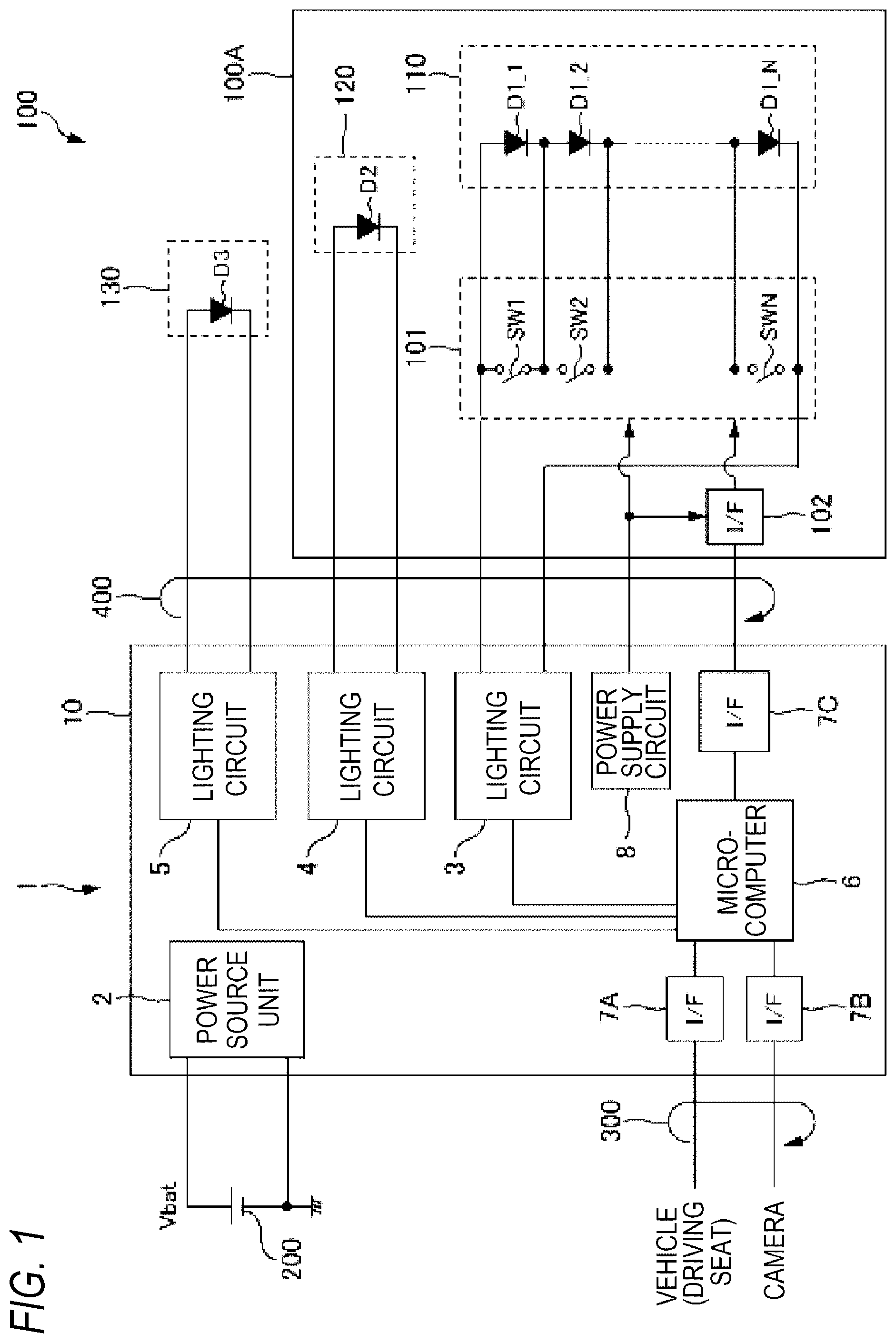
is a block diagram showing an example of a system configuration including a lighting control apparatus 1 according to the present embodiment.
is an exploded perspective view of the lighting control apparatus 1 .
is a conceptual view showing connection between the lighting control apparatus 1 and harnesses (a vehicle-side harness 300 and a lamp-side harness 400 ).
is a circuit diagram showing a configuration example of a lighting circuit 3 .
is a circuit diagram showing a configuration example of a lighting circuit 4 .
is a circuit diagram showing a configuration example of a lighting circuit 5 .
is an explanatory view of arrangement of components and the like on a +Z side surface of a substrate 10 .
is an explanatory view of arrangement of components and the like on a −Z side surface of the substrate 10 .
is a conceptual view showing connector arrangement according to a comparative example.
is a conceptual view showing connector arrangement according to the present embodiment.
DESCRIPTION OF EMBODIMENTS
At least the following matters will be clear based on the description of the present specification and accompanying drawings.
EMBODIMENT
<<System Configuration>>
is a block diagram showing an example of a system configuration including a lighting control apparatus 1 according to the present embodiment.
The lighting control apparatus 1 according to the present embodiment is an apparatus which is applied to a vehicle lamp 100 and controls lighting of each light source (described later) of the vehicle lamp 100 .
An input signal from a vehicle side is input to the lighting control apparatus 1 via a vehicle-side harness 300 . A power line of a power source voltage Vbat and a ground line of a ground level voltage from a battery 200 for a vehicle are input to the lighting control apparatus 1 . In the lighting control apparatus 1 , a grounded portion refers to a portion which is connected to the ground line of the battery 200 . The lighting control apparatus 1 is connected to light sources of the vehicle lamp 100 via a lamp-side harness 400 .
Before describing the lighting control apparatus 1 , the vehicle lamp 100 will be described.
The vehicle lamp 100 according to the present embodiment is, for example, a headlight provided at a front end portion of the vehicle, and includes a plurality of (here, three) light sources (light sources 110 , 120 , and 130 ). In the present embodiment, the light source 110 corresponds to a “first light source” or a “first light emission unit”, the light source 120 corresponds to a “second light source” or a “second light emission unit”, and the light source 130 corresponds to a “third light source” or a “third light emission unit”. It is noted that the light source 110 and the light source 120 are integrally provided as a light source unit 100 A. However, the present disclosure is not limited thereto, and the light source 110 and the light source 120 may be separately provided, or the light sources 110 , 120 , and 130 may be integrally provided.
The light source unit 100 A includes a switch circuit 101 , an interface circuit (hereinafter referred to as an I/F circuit) 102 , the light source 110 , and the light source 120 .
The switch circuit 101 is a circuit for switching elements to be lighted among a plurality (N) of light-emitting elements (D 1 _ 1 to D 1 _N) of the light source 110 (described later), and includes a plurality (N) of switches (SW 1 to SWN).
One end of the switch SW 1 is connected to a cathode of the light-emitting element D 1 _ 1 , and the other end of the switch SW 1 is connected to an anode of the light-emitting element D 1 _ 1 . That is, the switch SW 1 is connected in parallel with the light-emitting element D 1 _ 1 . Similarly, the switches SW 2 to SWN are connected in parallel with the light-emitting elements D 1 _ 2 to D 1 _N, respectively.
The I/F circuit 102 is communicably connected to an I/F circuit 7 C (described later) of a substrate 10 of the lighting control apparatus 1 , and receives a signal (a signal indicating an instruction from a microcomputer 6 ) from the I/F circuit 7 C. Based on the signal, the switches (SW 1 to SWN) of the switch circuit 101 are switched on and off.
The light source 110 is a high-beam light source. A high beam illuminates a front wide and distant range with a relatively high illuminance, and is mainly used when a vehicle runs at a high speed on a road where there are few oncoming vehicles or preceding vehicles. The light source 110 according to the present embodiment is an adaptive driving beam (ADB) in which the plurality of light-emitting elements D 1 _ 1 to D 1 _N are provided in series, and light distribution of a light distribution pattern is variably controlled by switching lighting of each light-emitting element. The ADB is a technique of recognizing a preceding vehicle, an oncoming vehicle, a pedestrian, and the like by an in-vehicle camera (imaging device), and increasing a forward field of vision of a driver at night without dazzling a driver and a pedestrian in front. In the present embodiment, each switch (SW 1 to SWN) of the switch circuit 101 is controlled to be turned on and off according to the instruction from the microcomputer 6 (described later) of the lighting control apparatus 1 , so that the corresponding light-emitting element is lighted.
The light source 120 is a low-beam light source and includes a light-emitting element D 2 . A low beam illuminates the vicinity of an own vehicle at a predetermined illuminance, has a determined light distribution regulation so as not to give glare to oncoming vehicles and preceding vehicles, and is mainly used when running in an urban area. In the present embodiment, the high-beam light source (the light source 110 ) is lighted together with (superimposed on) the low-beam light source (the light source 120 ). It is noted that in , the light source 120 includes one light-emitting element D 2 for simplification. However, the present disclosure is not limited thereto, and for example, a plurality of light-emitting elements D 2 may be connected in series.
The light source 130 has two functions of a daytime running lamp (DRL) and a clearance lamp (CLL), and includes a light-emitting element D 3 . The DRL is a lamp which is lighted to allow a driver of another vehicle and a pedestrian to visually recognize presence of the own vehicle more clearly during daytime, and the CLL is a lamp which is lighted to indicate a vehicle width of the own vehicle to another vehicle and a pedestrian during night-time (when the high beam and the low beam are not lighted). In the present embodiment, the DRL and the CLL are implemented by the same light source (the light source 130 ), and the functions thereof are implemented by modulating (changing a light emission amount of) the light-emitting element D 3 . It is noted that in , the light source 130 includes one light-emitting element D 3 for simplification. However, the present disclosure is not limited thereto, and for example, a plurality of light-emitting elements D 3 may be connected in series.
In the present embodiment, power consumption of the light source 110 (high beam) is larger than power consumption of the light source 120 (low beam) and power consumption of the light source 130 (DRL/CLL). In other words, the power consumption of the light source 120 and the power consumption of the light source 130 are smaller than the power consumption of the light source 110 . Further, the power consumption of the light source 130 is larger during the DRL than during the CLL. According to the present embodiment, the power consumption during the DRL is equal to or less than the power consumption of the light source 120 .
<<Configuration of Lighting Control Apparatus 1 >>
Next, the lighting control apparatus 1 according to the present embodiment will be described with reference to , 2 , and 3 . is an exploded perspective view of the lighting control apparatus 1 . is a conceptual view showing connection between the lighting control apparatus 1 and harnesses (the vehicle-side harness 300 and the lamp-side harness 400 ). In , three directions (an X direction, a Y direction, and a Z direction) orthogonal to one another are defined. The Z direction is, for example, an up-down direction (vertical direction), the Y direction is, for example, a direction (front-rear direction) along a longitudinal direction of the vehicle, and the X direction is, for example, a direction (left-right direction) along a vehicle width. In those directions, sides indicated by arrows are plus (+) sides, and opposite sides thereof are minus (−) sides. In the following description, for example, a plus side in the X direction is referred to as a +X side and a minus side in the X direction is referred to as a −X side.
As described above, the lighting control apparatus 1 is the apparatus which controls the lighting of each light source of the vehicle lamp 100 , and is attached to, for example, a bottom portion of a housing (not shown) of the vehicle lamp 100 .
As shown in , the lighting control apparatus 1 according to the present embodiment includes the substrate 10 , a cover 20 A, a cover 20 B, and a case 30 .
<Substrate 10 >
The substrate 10 is a member for mounting circuits (electronic components) constituting the lighting control apparatus 1 , and is implemented as a printed wiring substrate on which circuit wirings are formed. The substrate 10 according to the present embodiment has four sides including two sides (a side 10 A and a side 10 B) along the X direction and two sides (a side 10 C and a side 10 D) along the Y direction, and has a substantially quadrilateral shape with notched corners (see ). It is noted that in the substrate 10 according to the present embodiment, the corners are notched in a linear shape. However, the corners are not limited thereto, and for example, may be notched in an arc shape. Alternatively, the corners of the substrate 10 may not be notched (the substrate 10 may be quadrilateral). Further, each side of the substrate 10 may have an inwardly recessed portion or an outwardly protruding portion. Among the four sides of the substrate 10 according to the present embodiment, the side 10 A corresponds to a “predetermined side”.
As shown in , the substrate 10 is provided with a power circuit 2 , lighting circuits 3 to 5 , the microcomputer 6 , I/F circuits 7 A to 7 C, and a power supply circuit 8 . It is noted that in , for convenience, the circuits (the power source circuit 2 and the like) described above are omitted.
The power source circuit 2 is a circuit which generates, based on the power source voltage Vbat of the battery 200 , a drive voltage of each circuit (the microcomputer 6 and the like) provided on the substrate 10 .
The lighting circuit 3 is a circuit which lights the light source 110 of the vehicle lamp 100 . The lighting circuit 3 according to the present embodiment is a switching converter which generates a drive voltage corresponding to the light source 110 based on the power source voltage Vbat. The lighting circuit 3 corresponds to a “first switching converter” or a “first lighting circuit”, and the drive voltage corresponding to the light source 110 corresponds to a “first drive voltage”.
The lighting circuit 4 is a circuit which lights the light source 120 of the vehicle lamp 100 . The lighting circuit 4 according to the present embodiment is a switching converter which generates a drive voltage corresponding to the light source 120 based on the power source voltage Vbat. The lighting circuit 4 corresponds to a “second switching converter” or a “second lighting circuit”, and the drive voltage corresponding to the light source 120 corresponds to a “second drive voltage”.
The lighting circuit 5 is a circuit which lights the light source 130 of the vehicle lamp 100 . The lighting circuit 5 according to the present embodiment is a switching converter which generates a drive voltage corresponding to the light source 130 based on the power source voltage Vbat. The lighting circuit 5 corresponds to a “third switching converter” or a “third lighting circuit”, and the drive voltage corresponding to the light source 130 corresponds to a “third drive voltage”.
That is, in the lighting control apparatus 1 according to the present embodiment, the lighting circuits 3 to 5 (three switching converters) are provided on the substrate 10 . The configuration examples of the lighting circuits 3 to 5 will be described later.
The microcomputer 6 is a circuit which controls an operation of each part of the lighting control apparatus 1 and the vehicle lamp 100 . In the present embodiment, the microcomputer 6 corresponds to an “instruction circuit” which receives input signals from the I/F circuit 7 A and the I/F circuit 7 B and transmits instructions to the lighting circuits 3 to 5 . Based on the instructions (in other words, the input signals), the lighting circuits 3 to 5 light the corresponding light sources, respectively.
The I/F circuit 7 A is a circuit which receives the input signal from the vehicle (such as an operation unit of a driving seat) via the vehicle-side harness 300 and transmits the input signal to the microcomputer 6 .
The I/F circuit 7 B is a circuit which receives an input signal from an in-vehicle camera via the vehicle-side harness 300 and transmits the input signal to the microcomputer 6 . Each of the I/F circuit 7 A and the I/F circuit 7 B corresponds to an “interface circuit” which receives the input signal from the vehicle.
The I/F circuit 7 C transmits an output signal of the microcomputer 6 to the I/F circuit 102 of the light source unit 100 A via the lamp-side harness 400 .
The power supply circuit 8 is a circuit which supplies power for driving (operating) each circuit (the switch circuit 101 and the I/F circuit 102 ) of the light source unit 100 A to the light source unit 100 A.
As shown in , the substrate 10 is provided with an input region 11 , an output connector 12 , and ground portions 13 A, 13 B, and 13 C.
The input region 11 is a region where a plurality of input terminals (holes) of the substrate 10 are provided, and is a region into which input signals are input to the substrate 10 . In the present embodiment, the input region 11 is provided along the X direction in the vicinity of the side 10 A of the substrate 10 . An input connector 31 of the case 30 (described later) can be attached to the input region 11 .
The output connector 12 includes a plurality of connection terminals 12 a and two connection units 12 b.
The connection terminals 12 a are terminals for electrically connecting to the circuits (electronic components) provided on the substrate 10 , and the plurality of the connection terminals 12 a are provided along a longitudinal direction (here, the Y direction) on both outer sides of the output connector 12 in a transverse direction (here, the X direction).
The connection unit 12 b is a unit to be engaged with a connector 410 of the lamp-side harness 400 . When the connector 410 is fitted into the connection unit 12 b of the output connector 12 , the output connector 12 and the lamp-side harness 400 are electrically connected. It is noted that the output connector 12 according to the present embodiment includes the two connection units 12 b provided side by side in the Y direction, so that two connectors 410 can be connected. However, the present disclosure is not limited thereto. For example, one connector 410 may be connected to only one connection unit 12 b.
The ground portions 13 A, 13 B, and 13 C are parts coming into conductive contact with the cover 20 A. Through holes are formed in the ground portions 13 A, 13 B, and 13 C, respectively, and a conductor connected to the ground (the ground line) is exposed from a surface (a substrate surface around each through hole). When the substrate 10 and the cover 20 A are fastened to the case 30 by screws 41 , the ground portions 13 A, 13 B, and 13 C come into conductive contact with the cover 20 A. Specifically, the ground portion 13 A comes into conductive contact with a connection piece 23 A of the cover 20 A, the ground portion 13 B comes into conductive contact with a connection piece 23 B of the cover 20 A, and the ground portion 13 C comes into conductive contact with a connection piece 23 C of the cover 20 A. The ground portion 13 B corresponds to “one part of a first conduction part and a second conduction part”, and the ground portion 13 A is the “other part of the first conduction part and the second conduction part”. Further, the ground portion 13 C corresponds to a “third conduction part”.
<Cover 20 A>
The cover 20 A is a noise shielding member which reduces or prevents leakage of electromagnetic noise generated from the circuit components provided on the substrate 10 and shields electromagnetic noise entering from an outside, and is formed of a conductive material (for example, a metal such as aluminum). The cover 20 A is a box-shaped member having a substantially quadrilateral shape corresponding to the substrate 10 in a plan view and open on a −Z side, and is placed on a +Z side of the substrate 10 and accommodated in the case 30 .
The cover 20 A includes an opening 22 and the connection pieces 23 A, 23 B, and 23 C.
The opening 22 is a portion (opening) through which the output connector 12 of the substrate 10 is inserted when the substrate 10 is attached to the case 30 together with the cover 20 A. Therefore, the opening 22 is formed at a position and in a shape corresponding to the output connector 12 . The opening 22 allows the connector 410 of the lamp-side harness 400 to be fitted into the connection unit 12 b of the output connector 12 . The cover 20 A according to the present embodiment covers at least a portion excluding the input region 11 and the output connector 12 in a +Z side surface of the substrate 10 , and covers all components of the lighting circuits 3 to 5 provided in the +Z side surface of the substrate 10 . However, the present disclosure is not limited thereto, and at least a part of the components in each of the lighting circuits 3 to 5 may be covered. The +Z side surface of the substrate 10 corresponds to “one surface”, and the cover 20 A corresponds to a “first cover”.
The connection pieces 23 A, 23 B, and 23 C are portions for fixing (mounting) the cover 20 A to the case 30 together with the substrate 10 by the screws 41 . The connection pieces 23 A, 23 B, and 23 C are provided at positions corresponding to the ground portions 13 A, 13 B, and 13 C of the substrate 10 to extend laterally from a side surface of the cover 20 A. Further, the connection pieces 23 A, 23 B, and 23 C are provided with through holes through which the screws 41 are inserted at positions corresponding to the through holes of the ground portions 13 A, 13 B, and 13 C, respectively.
<Cover 20 B>
Similarly to the cover 20 A, the cover 20 B is a noise shielding member, and is formed of a conductive material (for example, aluminum) to have a shallow box shape corresponding to the substrate 10 . In the present embodiment, the cover 20 B for noise shielding covers a −Z side surface of the substrate 10 . Accordingly, noise can be reduced on both sides of the substrate 10 in the Z direction. The cover 20 B has engagement holes 24 .
The engagement holes 24 are holes for fixing the cover 20 B to the case 30 , and are provided at positions corresponding to engagement protrusions 34 (described later) of the case 30 .
By engaging the engagement holes 24 with the engagement protrusions 34 of the case 30 in a state where the substrate 10 and the cover 20 A are attached (fastened), the cover 20 B is fixed to the case 30 while covering the −Z side surface of the substrate 10 . Accordingly, the noise can be reduced or prevented (shielded) even on a −Z side of the substrate 10 , and the noise can be further reduced. The cover 20 B is fixed to the case 30 by applying an adhesive (not shown) between an outer edge of the case 30 and the cover 20 B and curing the adhesive. Since the adhesive is interposed between the cover 20 B and the case 30 , a waterproof structure for reducing or preventing water from entering is also achieved.
The cover 20 B is not accommodated in the case 30 and is exposed. Accordingly, the cover 20 B also has a function of dissipating heat generated in the substrate 10 via heat transfer sheets 42 . The heat transfer sheets 42 are members which are interposed between the substrate 10 and the cover 20 B, transfer the heat generated in the substrate 10 to the cover 20 B, and also reduce or prevent vibration.
<Case 30 >
The case 30 is a housing which accommodates therein the cover 20 A and the substrate 10 of the lighting control apparatus 1 , and is formed of, for example, a resin. The case 30 according to the present embodiment includes the input connector 31 , a cylindrical opening 32 , and the engagement protrusions 34 .
The input connector 31 is a connector for connecting to a connector 310 of the vehicle-side harness 300 , and corresponds to a “second connector”. The input connector 31 according to the present embodiment is provided on a −Y side end of the case 30 . The input connector 31 is provided with a plurality of pins 31 a , and the pins 31 a are bent to the −Z side inside the case 30 . That is, when the substrate 10 is attached to the case 30 , the pins 31 a are inserted into corresponding terminals (holes) of the input region 11 . Then, by soldering the terminals of the input region 11 and the inserted pins 31 a , respectively, the terminals of the input region 11 and the pins 31 a of the input connector 31 are electrically connected, respectively. Accordingly, the input connector 31 is attached to the input region 11 of the substrate 10 , and a signal (an input signal) can be input to the substrate 10 via the input connector 31 of the case 30 . The input connector 31 is shaped to have a waterproof structure when the connector 310 is connected.
The cylindrical opening 32 is an opening through which the lamp-side harness 400 is inserted into the case 30 , and is provided at a position corresponding to the output connector 12 of the substrate 10 and the opening 22 of the cover 20 A in a +Z side surface of the case 30 . The connector 410 of the lamp-side harness 400 is fitted into the connection unit 12 b of the output connector 12 through the cylindrical opening 32 of the case 30 . Further, an edge of the cylindrical opening 32 protrudes in a cylindrical shape toward the +Z side, and the protruded portion is fitted into, for example, a bottom portion of a housing (not shown) of the vehicle lamp 100 . Accordingly, the case 30 (in other words, the lighting control apparatus 1 ) is attached to the housing of the vehicle lamp 100 . When the lighting control apparatus 1 is attached, each portion of the lighting control apparatus 1 and a connection portion with each harness is subjected to waterproof measures by using, for example, a sealing material and an adhesive to reduce or prevent the water from entering.
The engagement protrusions 34 are protruded portions for fixing the cover 20 B, and are provided on both side portions of the case 30 in the X direction to protrude outward.
<Lighting Circuits 3 , 4 , and 5 >
As described above, the lighting circuits 3 , 4 , and 5 according to the present embodiment are implemented by switching converters.
is a circuit diagram showing the configuration example of the lighting circuit 3 . is a circuit diagram showing the configuration example of the lighting circuit 4 . is a circuit diagram showing the configuration example of the lighting circuit 5 . An NMOSFET is used for each transistor (a transistor M 3 A and the like) in to 6 .
The lighting circuit 3 is a circuit which generates the drive voltage corresponding to the light source 110 based on the power source voltage Vbat. As shown in , the lighting circuit 3 according to the present embodiment includes a boost circuit 3 A and a step-down circuit 3 B.
The boost circuit 3 A is a circuit which increases the power source voltage Vbat, and includes a control circuit IC 3 A, capacitors C 3 A 1 and C 3 A 2 , a coil L 3 A, the transistor M 3 A, a diode D 3 A, and resistors R 3 A 1 and R 3 A 2 .
One end of the capacitor C 31 A 1 is connected to the power source line, and the other end is connected to the ground line (grounded).
One end of the coil L 3 A is connected to the one end of the capacitor C 3 A 1 , and the other end of the coil L 3 A is connected to a drain of the transistor M 3 A and an anode of the diode D 3 A.
A source of the transistor M 3 A is grounded, and a signal from the control circuit IC 3 A is input into a gate of the transistor M 3 A.
A cathode of the diode D 3 A is connected to one end of the capacitor C 3 A 2 , and the other end of the capacitor C 3 A 2 is grounded. A voltage at a connection point between the cathode of the diode D 3 A and the capacitor C 3 A 2 is an output voltage of the boost circuit 3 A.
The resistor R 3 A 1 and the resistor R 3 A 2 are connected in series and are provided in parallel with the capacitor C 3 A 2 .
The control circuit IC 3 A is a circuit which controls an operation of the lighting circuit 3 (here, the boost circuit 3 A) based on the instruction from the microcomputer 6 , and corresponds to a “first control circuit”. In the present embodiment, the control circuit IC 3 A (and control circuits IC 3 B, IC 4 , and IC 5 to be described later) is implemented by an integrated circuit (IC). Based on a divided voltage between the resistor R 3 A 1 and the resistor R 3 A 2 (a voltage at a connection point between the resistor R 3 A 1 and the resistor R 3 A 2 ), the control circuit IC 3 A controls the transistor M 3 A to be turned on and off such that the output voltage of the boost circuit 3 A (a voltage of the capacitor C 3 A 2 ) becomes a predetermined voltage.
When the transistor M 3 A is turned on by the control circuit IC 3 A, energy from power source is stored in the coil L 3 A. When the transistor M 3 A is turned off, a voltage corresponding to the energy stored in the coil L 3 A is superimposed on the power source voltage Vbat. Therefore, the output voltage of the boost circuit 3 A is higher than the power source voltage Vbat.
The step-down circuit 3 B is a circuit which steps down the output voltage of the boost circuit 3 A to generate the drive voltage corresponding to the light source 110 , and includes a control circuit IC 3 B, a capacitor C 3 B, coils L 3 B 1 and L 3 B 2 , and a resistor R 3 B.
The control circuit IC 3 B controls an operation of the lighting circuit 3 (here, the step-down circuit 3 B) based on an instruction from the microcomputer 6 . The control circuit IC 3 B includes a transistor M 3 B 1 and a transistor M 3 B 2 . Each of the transistor M 3 B 1 and the transistor M 3 B 2 corresponds to a “switch element”.
A drain of the transistor M 3 B 1 is connected to the one end of the capacitor C 3 A 1 of the boost circuit 3 A. That is, the output voltage of the boost circuit 3 A is applied to the drain of the transistor M 3 B 1 . A source of the transistor M 3 B 1 is connected to a drain of the transistor M 3 B 2 and one end of the capacitor C 3 B, and a source of the transistor M 3 B 2 and the other end of the capacitor C 3 B are grounded.
The coil L 3 B 1 , the resistor R 3 B, and the coil L 3 B 2 are connected in series. One end of the coil L 3 B 1 is connected to a connection point between the transistor M 3 B 1 , the transistor M 3 B 2 , and the capacitor C 3 B. In the present embodiment, the capacitor C 3 B corresponds to a “first output capacitor”.
The control circuit IC 3 B controls (controls on and off) gate voltages of the transistor M 3 B 1 and the transistor M 3 B 2 based on a current flowing through the resistor R 3 B.
When the transistor M 3 B 1 is turned on and the transistor M 3 B 2 is turned off, an input voltage (the output voltage of the boost circuit 3 A) of the step-down circuit 3 B is applied to the one end of the coil L 3 B 1 . When the transistor M 3 B 1 is turned off and the transistor M 3 B 2 is turned on, a voltage of the ground line (a ground voltage) is applied to the one end of the coil L 3 B 1 .
By repeating the operation described above, an output voltage of the step-down circuit 3 B becomes lower than the input voltage (the output voltage of the boost circuit 3 A). Accordingly, the output voltage (the drive voltage) of the step-down circuit 3 B is adjusted by the control circuit IC 3 B such that a predetermined drive current flows through the light-emitting element to be lighted among the light-emitting elements D 1 _ 1 to D 1 _N of the light source 110 .
The lighting circuit 4 is a circuit which generates the drive voltage corresponding to the light source 120 based on the power source voltage Vbat. As shown in , the lighting circuit 4 has a configuration of a so-called H-bridge type switching converter, and includes transistors M 41 , M 42 , M 43 , and M 44 , a coil L 4 , capacitors C 41 and C 42 , a resistor R 15 , and a control circuit IC 4 .
One end of the capacitor C 41 is connected to the power source line, and the other end of the capacitor C 41 is connected to the ground line (grounded).
A drain of the transistor M 41 is connected to one end of the capacitor C 41 , and a source of the transistor M 41 is connected to a drain of the transistor M 42 and one end of the coil L 4 .
The other end of the coil L 4 is connected to a source of the transistor M 43 and a drain of the transistor M 44 . A source of the transistor M 42 and a source of the transistor M 44 are grounded.
One end of the capacitor C 42 is connected to a drain of the transistor M 43 , and the other end of the capacitor C 42 is grounded. A voltage at the one end of the capacitor C 42 is output via the resistor R 4 . In the present embodiment, the capacitor C 42 corresponds to a “second output capacitor”.
The control circuit IC 4 is a circuit which controls an operation of the lighting circuit 4 based on an instruction from the microcomputer 6 , and corresponds to a “second control circuit”. The control circuit IC 4 controls on and off of the transistors (the transistors M 41 , M 42 , M 43 , and M 44 ) such that a current flowing through the resistor R 4 (in other words, the light-emitting element D 2 of the light source 120 ) becomes a target value (a predetermined drive current).
An operation of such an H-bridge type circuit is known. A brief explanation of the operation is that, by fixing the transistor M 43 to be turned on and the transistor M 44 to be turned off and controlling on and off of the transistors M 41 and M 42 , power can be supplied from an input side to an output side while being stepped down (a step-down mode).
Further, by fixing the transistor M 41 to be turned on and the transistor M 42 to be turned off and controlling on and off of the transistors M 43 and M 44 , power can be supplied from the input side to the output side while being boosted (a boost mode).
By performing the step-down mode or the boost mode in this manner, it is possible to generate the drive voltage according to a load (here, the light source 120 ) based on the power source voltage Vbat.
The lighting circuit 5 is a circuit which generates the drive voltage corresponding to the light source 130 based on the power voltage Vbat. As shown in , the lighting circuit 5 also has a configuration of an H-bridge type switching converter, and includes transistors M 51 , M 52 , M 53 , and M 54 , a coil L 5 , capacitors C 51 and C 52 , a resistor R 5 , and a control circuit IC 5 . The control circuit IC 5 is a circuit which controls an operation of the lighting circuit 5 based on an instruction from the microcomputer 6 , and corresponds to a “third control circuit”.
A configuration and an operation of the lighting circuit 5 are the same as those of the lighting circuit 4 , and description thereof is omitted.
<<Arrangement of Components on Substrate 10 >>
is an explanatory view of an arrangement example of components and the like in the +Z side surface of the substrate 10 . is an explanatory view of an arrangement example of components and the like in the −Z side surface of the substrate 10 .
The substrate 10 according to the present embodiment is a substrate having a substantially quadrilateral shape as described above, and is provided with the input region 11 , the output connector 12 , and the ground portions 13 A, 13 B, and 13 C. In , a dashed-and-dotted line indicates an axis along the Y direction passing through a middle point of the output connector 12 in the transverse direction. In the present embodiment, a middle point of the side 10 A of the substrate 10 is located on the axis (the dashed-and-dotted line). In the present embodiment, the X direction corresponds to a “predetermined direction”.
The ground portion 13 A is provided at a corner portion between the side 10 A and the side 10 D of the substrate 10 (on the +X side relative to the dashed-and-dotted line), and the ground portion 13 B is provided on the side 10 B on the +X side relative to the dashed-and-dotted line. The ground portion 13 C is provided at a corner portion between the side 10 C and the side 10 A (on the −X side relative to the dashed-and-dotted line). The input region 11 is provided along the X direction in the vicinity of the side 10 A.
As shown in , the electronic components of the circuits constituting the lighting control apparatus 1 are mounted on the substrate 10 .
<Arrangement of Lighting Circuits 3 , 4 , and 5 >
In the present embodiment, three lighting circuits (the lighting circuits 3 , 4 , and 5 ) are provided on the same substrate 10 . Each of the lighting circuits 3 , 4 , and 5 is implemented by a switching converter including a transistor (a switching element), a coil, and a capacitor. Such a switching converter tends to generate more electromagnetic noise than a linear regulator (a series regulator). In particular, more noise tends to be generated in an output-side circuit of the switching converter (the lighting circuit 3 in the present embodiment) having a large drive capability (power consumption). In the present embodiment, the cover 20 A for noise shielding is provided to cover the +Z side surface (the lighting circuits 3 to 5 ) of the substrate 10 . However, a sufficient noise reduction effect may not be obtained in the lighting circuit 3 having large power consumption.
Therefore, in the present embodiment, as shown in , the lighting circuit 3 is provided between the ground portion 13 A and the ground portion 13 B which are the parts of the substrate 10 coming into conductive contact with the cover 20 A, and the capacitor C 3 B on the output side where the noise tends to be generated is provided in the vicinity of the ground portion 13 B. Accordingly, the noise reduction effect can be improved, and the noise can be reduced.
In addition, the coils L 3 B 1 and L 3 B 2 of the lighting circuit 3 are also provided in the vicinity of the ground portion 13 B. Accordingly, the noise can be further reduced.
Further, the lighting circuit 3 according to the present embodiment includes the boost circuit 3 A which boosts the power source voltage Vbat and the step-down circuit 3 B which steps down the output voltage of the boost circuit 3 A and generates the drive voltage corresponding to the light source 110 . The capacitor C 3 B and the coils L 3 B 1 and L 3 B 2 are used in the step-down circuit 3 B. That is, by providing the capacitor C 3 B and the coils L 3 B 1 and L 3 B 2 of the step-down circuit 3 B in the vicinity of the ground portion 13 B in this manner, the noise can be efficiently reduced.
In the present embodiment, the vicinity of the ground portion 13 B is a range shorter than a distance from the ground portion 13 B to the control circuit IC 3 B (the transistors M 3 B 1 and M 3 B 2 in the control circuit IC 3 B) of the step-down circuit 3 B. By providing the capacitor C 3 B and the coils L 3 B 1 and L 3 B 2 of the lighting circuit 3 within the range, the noise reduction effect can be improved.
In the present embodiment, the ground portion 13 A, the ground portion 13 B, and the lighting circuit 3 are provided on the plus side (the +X side relative to the dashed-and-dotted line) of the substrate 10 in the X direction, and the lighting circuit 4 and the lighting circuit 5 are provided on the minus side (the −X side relative to the dashed-and-dotted line) of the substrate 10 in the X direction. Accordingly, heat generation is equalized. The plus side in the X direction corresponds to “one side in a predetermined direction”, and the minus side in the X direction corresponds to “the other side in the predetermined direction”.
As described above, the ground portion 13 C is provided on the minus side of the substrate 10 in the X direction, and the lighting circuit 4 is provided closer to the ground portion 13 C than the lighting circuit 5 . As shown in , a distance between the capacitor C 3 B of the lighting circuit 3 and the ground portion 13 B is shorter than a distance between the capacitor C 42 on the output side of the lighting circuit 4 and the ground portion 13 C. The distance between the capacitor C 3 B of the lighting circuit 3 and the ground portion 13 B corresponds to a “first distance”, and the distance between the capacitor C 42 of the lighting circuit 4 and the ground portion 13 C corresponds to a “second distance”. Accordingly, it is possible to improve the arrangement (a degree of freedom of layout) of the lighting circuits 4 and 5 while reducing the noise.
<Arrangement of Output Connector 12 >
The output connector 12 according to the present embodiment is a rectangular connector having the longitudinal direction and the transverse direction. The plurality of connection terminals 12 a are provided along the longitudinal direction on both outer sides of the output connector 12 in the transverse direction.
For example, if the output connector 12 is provided on the substrate 10 such that the longitudinal direction is parallel to the side 10 A, a length of a wiring pattern may become larger and it may be difficult to reduce a size of the substrate 10 .
is a conceptual view showing connector arrangement according to a comparative example. is a conceptual view showing connector arrangement according to the present embodiment.
In the comparative example ( ), two output connectors 14 are provided. The output connector 14 is a connector corresponding to one of the connection units 12 b of the output connector 12 , and includes a plurality of (ten on one side) connection terminals 14 a and a connection unit 14 b . In , each of the two output connectors 14 is provided such that a longitudinal direction of the output connector 14 is parallel to the X direction (a direction along the input region 11 ), and the plurality of connection terminals 14 a are provided along the longitudinal direction (here, the X direction) on both outer sides of the output connector 14 in a transverse direction (here, the Y direction).
In a case of this comparative example ( ), it is necessary to bend wiring patterns connecting components provided on the substrate 10 and the connection terminals 14 a of the output connector 14 as shown in the drawing, and it is difficult to route wirings. Therefore, it is difficult to reduce the substrate size. In , the two output connectors 14 are provided, and when the output connector 12 is provided such that the longitudinal direction of the output connector 12 is along the X direction, similarly, it is also difficult to route the wirings and it is difficult to reduce the substrate size.
On the other hand, in the present embodiment, as shown in , the output connector 12 is provided such that the longitudinal direction of the output connector 12 intersects the side 10 A (the input region 11 ). In the present embodiment, the longitudinal direction of the output connector 12 is orthogonal to the input region 11 (the X direction), but is not limited thereto and may be substantially orthogonal.
Accordingly, the circuits (the lighting circuits and the like) can be provided on both sides of the output connector 12 in the transverse direction (the X direction), and the wirings connecting the components provided on the substrate 10 and the connection terminals 12 a of the output connector 12 can be easily routed. Accordingly, wiring efficiency can be improved and the substrate size can be reduced as compared with the comparative example ( ).
As described above, in , the lighting circuit 3 having the large power consumption is provided on the +X side relative to the dashed-and-dotted line. In this case, as shown in , the lighting circuit 3 can be connected to at least a part of the plurality of connection terminals 12 a of the output connector 12 on the +X side. Further, in , the lighting circuits 4 and 5 are provided on the −X side relative to the dashed-and-dotted line. In this case, as shown in , the lighting circuits 4 and 5 can be connected to at least a part of the plurality of connection terminals 12 a of the output connector 12 on the −X side. Accordingly, it is possible to improve the wiring efficiency for the three lighting circuits.
The I/F circuits 7 A and 7 B are provided between the side 10 A (the input region 11 ) and the output connector 12 (see ). Accordingly, wirings from the I/F circuits 7 A and 7 B to the lighting circuits (the lighting circuits 3 to 5 ) can be formed shorter, and the wiring efficiency can be further improved.
Further, as shown in , the output connector 12 and the I/F circuits 7 A and 7 B are provided on the +Z side surface of the substrate 10 . The microcomputer 6 , the control circuit IC 3 of the lighting circuit 3 , the control circuit IC 4 of the lighting circuit 4 , and the control circuit IC 5 of the lighting circuit 5 are provided on the −Z side surface of the substrate 10 . Accordingly, the substrate size can be reduced as compared with a case where all the components are provided on the +X side of the substrate 10 . Further, a heat dissipation performance can be improved by providing the circuits (the microcomputer 6 , the control circuit IC 3 , the control circuit IC 4 , and the control circuit IC 5 ) which tend to generate heat in the −Z side surface (a cover 20 B side) of the substrate 10 .
As described above, the middle point of the side 10 A of the substrate 10 is located on the axis (the dashed-and-dotted line) along the Y direction passing through the middle point of the output connector 12 in the transverse direction (here, the X direction). Accordingly, the circuits (the lighting circuits 3 to 5 and the like) can be easily provided on both sides of the output connector 12 in the transverse direction.
SUMMARY
The lighting control apparatus 1 according to the present embodiment has been described above. The lighting control apparatus 1 includes: the lighting circuit 3 which includes the transistors M 3 B 1 and M 3 B 2 , the coils L 3 B 1 and L 3 B 2 , and the capacitor C 3 B 2 and is configured to generate a drive voltage corresponding to the light source 110 of the vehicle lamp 100 based on the power source voltage Vbat; the substrate 10 on which the lighting circuit 3 is provided; and a cover 20 A which is formed of a conductive material and covers at least a part of components of the lighting circuit 3 in a +Z side surface of the substrate 10 . The substrate 10 includes the ground portion 13 A and the ground portion 13 B which are in conductive contact with the cover 20 A. The lighting circuit 3 is provided between the ground portion 13 A and the ground portion 13 B. The capacitor C 3 B 2 is provided in a vicinity of the ground portion 13 B. Accordingly, it is possible to reduce noise caused by the lighting circuit 3 having larger power consumption.
The lighting control apparatus 1 may further include the cover 20 B which is formed of a conductive material and covers a −Z side surface of the substrate 10 . Accordingly, the noise can be reduced or prevented (shielded) even on the −Z side of the substrate 10 , and the noise can be reduced on both sides of the substrate 10 in the Z direction.
Further, the coils L 3 B 1 and L 3 B 2 may be provided in the vicinity of the ground portion 13 B. Accordingly, the noise can be further reduced.
Further, the lighting circuit 3 may include: the boost circuit 3 A which is configured to boost the power source voltage Vbat and the step-down circuit 3 B which is configured to step down an output voltage of the boost circuit 3 A and generate a drive voltage corresponding to the light source 110 . The capacitor C 3 B 2 and the coils L 3 B 1 and L 3 B 2 may be used in the step-down circuit 3 B. Accordingly, the noise can be efficiently reduced.
The vicinity of the ground portion 13 B may be a range shorter than a distance from the ground portion 13 B to the control circuit IC 3 B (the transistor M 3 B 1 and M 3 B 2 ). By providing a noise source (the capacitor C 3 B 2 ) within the range, the noise reduction effect can be improved.
The lighting control apparatus 1 may further include: the lighting circuit 4 which is configured to generate a drive voltage corresponding to the light source 120 having power consumption smaller than that of the light source 110 based on the power source voltage Vbat; and the lighting circuit 5 which is configured to generate a drive voltage corresponding to the light source 130 having power consumption smaller than that of the light source 110 based on the power source voltage Vbat. The ground portion 13 A, the ground portion 13 B, and the lighting circuit 3 may be provided on a plus side relative to a middle point of the substrate 10 in the X direction, and the lighting circuit 4 and the lighting circuit 5 may be provided on a minus side relative to the middle point of the substrate 10 in the X direction. Accordingly, heat generation can be equalized.
The substrate 10 may further include the ground portion 13 C which is in conductive contact with the cover 20 A on the minus side in the X direction. The lighting circuit 4 may be provided closer to the ground portion 13 C than the lighting circuit 5 . A distance between the capacitor C 3 B 2 of the lighting circuit 3 and the ground portion 13 B may be smaller than a distance between the capacitor C 42 of the lighting circuit 4 and the ground portion 13 C. Accordingly, it is possible to improve the arrangement (a degree of freedom of layout) of the lighting circuits 4 and 5 while reducing the noise.
The lighting control apparatus 1 includes: the substrate 10 which has a substantially quadrilateral shape; the output connector 12 which is provided on the substrate 10 and configured to supply power to a light source used in the vehicle lamp 100 ; and the input region 11 which is provided on the substrate 10 along the side 10 A of the substrate 10 and to which the input connector 31 configured to receive an input signal from a vehicle can be attached. The output connector 12 has a longitudinal direction intersecting the input region 11 (the X direction in the present embodiment) and a transverse direction. A plurality of connection terminals 12 a are provided along the longitudinal direction on both outer sides of the output connector 12 in the transverse direction. Accordingly, as compared with a case where the output connector 12 is provided such that a longitudinal direction thereof is parallel to the input area (see ), wiring efficiency can be improved and a substrate size can be reduced.
The lighting control apparatus 1 may further include: the case 30 which is provided with the input connector 31 . In a stat where the substrate 10 is attached to the case 30 , the input signal is input to the substrate 10 via the input connector 31 . Accordingly, a size of the substrate 10 can be reduced.
The substrate 10 may be provided with the lighting circuit 3 which is configured to light, among light sources included in the vehicle lamp 100 , the light source 110 based on the input signal, the lighting circuit 4 which is configured to light the light source 120 having power consumption smaller than that of the light source 110 based on the input signal, and the lighting circuit 5 which is configured to light the light source 130 having power consumption smaller than that of the light source 110 based on the input signal. The lighting circuit 3 may be provided on one side (the +X side) of the output connector 12 in the transverse direction and is connected to at least a part of the plurality of connection terminals 12 a on the +X side. The lighting circuit 4 and the lighting circuit 5 may be provided on the other side (the −X side) of the output connector 12 in the transverse direction and may be connected to at least a part of the plurality of connection terminals 12 a on the −X side. Accordingly, it is possible to improve the wiring efficiency for the three lighting circuits (the lighting circuits 3 , 4 , and 5 ).
The substrate 10 may be provided with the interface circuits 7 A and 7 B which are configured to receive the input signal, and the interface circuits 7 A and 7 B may be provided between the side 10 A and the output connector 12 in the Y direction (the longitudinal direction of the output connector 12 ). Accordingly, wirings from the input region 11 to the lighting circuits (the lighting circuits 3 to 5 ) can be formed shorter, and the wiring efficiency can be further improved.
The lighting control apparatus 1 may further include: the microcomputer 6 which is configured to receive a signal from the I/F circuits 7 A and 7 B and transmit instructions to the lighting circuits 3 , 4 , and 5 . The lighting circuit 3 may include the control circuit IC 3 A which is configured to control an operation of the lighting circuit 3 (specifically, the boost circuit 3 A) based on an instruction of the microcomputer 6 . The lighting circuit 4 may include the control circuit IC 4 which is configured to control an operation of the lighting circuit 4 based on an instruction of the microcomputer 6 . The lighting circuit 4 may include the control circuit IC 5 which is configured to control an operation of the lighting circuit 5 based on an instruction of the microcomputer 6 . The output connector 12 and the I/F circuits 7 A and 7 B may be provided on a +X side surface of the substrate 10 . The microcomputer 6 , the control circuit IC 3 A of the lighting circuit 3 , the control circuit IC 4 of the lighting circuit 4 , and the control circuit IC 5 of the lighting circuit 5 may be provided on a −X side surface of the substrate 10 . Accordingly, the substrate size can be reduced as compared with a case where all the components are provided on the +X side of the substrate 10 . Further, a heat dissipation performance can be improved by providing the circuits (the microcomputer 6 , the control circuit IC 3 , the control circuit IC 4 , and the control circuit IC 5 ) which tend to generate heat in the −Z side surface (a cover 20 B side) of the substrate 10 .
A middle point of the side 10 A in the vicinity of the input region 11 of the substrate 10 may be located on an axis (a dashed-and-dotted line in the drawing) along the Y direction passing through a middle point of the output connector 12 in the transverse direction (here, the X direction). Accordingly, the circuits (the lighting circuits 3 to 5 and the like) can be easily provided on both sides of the output connector 12 in the transverse direction.
The embodiment described above is intended to facilitate understanding of the present disclosure, and is not to be construed as limiting the present disclosure. In addition, it is needless to say that the present disclosure can be changed or improved without departing from the inventive concept thereof, and equivalents thereof are included in the present disclosure.
The present application is based on Japanese Patent Application (Application No. 2021-077428) filed on Apr. 30, 2021 and Japanese Patent Application (Application No. 2021-077429) filed on Apr. 30, 2021, and the contents thereof are incorporated herein by reference.
INDUSTRIAL APPLICABILITY
According to the present disclosure, it is possible to provide a lighting control apparatus capable of reducing noise. Further, according to the present disclosure, it is possible to provide a lighting control apparatus capable of improving wiring efficiency and reducing a substrate size.
REFERENCE SIGNS LIST
•
• 1 lighting control apparatus • 2 power source circuit • 3 lighting circuit • 3 A boost circuit • 3 B step-down circuit • 4 lighting circuit • 5 lighting circuit • 6 microcomputer • 7 A, 7 B, 7 C I/F circuit • 8 power supply circuit • 10 substrate • 10 A, 10 B, 10 C, 10 D side • 11 input region • 12 output connector • 12 a connection terminal • 12 b connection unit • 13 A, 13 B, 13 C ground portion • 14 output connector • 14 a connection terminal • 14 b connection unit • 20 A, 20 B cover • 22 opening • 23 A, 23 B, 23 C connection piece • 24 engagement hole • 30 case • 31 input connector • 32 cylindrical opening • 34 engagement protrusion • 41 screw • 42 heat transfer sheet • 100 vehicle lamp • 100 A light source unit • 101 switch circuit • 110 light source • 120 light source • 130 light source • 200 battery • 300 vehicle-side harness • 310 connector • 400 lamp-side harness • 410 connector • D 1 _ 1 to D 1 _N, D 2 , D 3 light-emitting element • SW 1 to SWN switch • Vbat power source voltage • D 3 A diode • C 3 A 1 , C 3 A 2 , C 3 B, C 41 , C 42 , C 51 , C 52 capacitor • L 3 A, L 3 B 1 , L 3 B 2 , L 4 , L 5 coil • R 3 A 1 , R 3 A 2 , R 3 B, R 4 , R 5 resistor • IC 3 A, IC 3 B, IC 4 , IC 5 control circuit • M 3 A, M 3 B 1 , M 3 B 2 , M 41 to M 44 , M 51 to M 54 transistor
Figures (8)
Citations
This patent cites (17)
- US6320762
- US2012/0262432
- US2014/0112015
- US2014/0203705
- US2015/0305109
- US2016/0181940
- US2018/0339641
- US2019/0180930
- US2019/0223318
- US104518682
- US2012-113832
- US2014-082147
- US2018-198173
- US2019-125443
- US2019125433
- US20200112198
- USWO-2018055979