Abstract
A semiconductor device having: a semiconductor device unit including an output element and a sensing element; and a control circuit. When the output element is in an on state, the control circuit connects a high potential terminal of a sensing element to a high potential terminal of an output element and ungrounds a low potential terminal of the sensing element to cause the sensing element to function as a current sensing element for detecting a current flowing in the output element. When the output element is in an off state, the control circuit disconnects the high potential terminals of the sensing element and the output element, causes a constant current to flow through the high potential terminal of the sensing element, and grounds the low potential terminal of the sensing element to cause the sensing element to function as a temperature sensing element for detecting the temperature of the output element.
Claims (7)
1. A semiconductor device for driving a load, comprising: a semiconductor device unit, including an output element that performs switching to operate the load, the output element having a high potential terminal, and a sensing element having a high potential terminal and a low potential terminal; and a control circuit coupled to the semiconductor device unit, the control circuit being configured to be operable, when the output element is in an on state, to turn on the sensing element by connecting the high potential terminal of the sensing element to the high potential terminal of the output element and ungrounding the low potential terminal of the sensing element, to thereby cause the sensing element to function as a current sensing element for detecting a current flowing in the output element, and when the output element is in an off state, to cut off a connection between the high potential terminal of the sensing element and the high potential terminal of the output element, to supply a constant current from the high potential terminal of the sensing element in a state where the low potential terminal of the sensing element is grounded, to thereby turn on the sensing element and cause the sensing element to function as a temperature sensing element for detecting a temperature of the output element.
Show 6 dependent claims
2. The semiconductor device according to claim 1 , wherein the control circuit includes: a logic circuit, a constant current source having an output end, a first switch that connects or disconnects the output end of the constant current source and the high potential terminal of the sensing element, and a second switch that grounds or ungrounds the low potential terminal of the sensing element; the semiconductor device further includes a third switch that connects or disconnects the high potential terminal of the sensing element and the high potential terminal of the output element and that is disposed inside or outside the semiconductor device unit; and the logic circuit is configured to generate and output, based on a level of a driving control signal for switching the output element and a level of a temperature detection control signal, a first switching control signal for performing switching control of the first switch, a second switching control signal for performing switching control of the second switch, and a third switching control signal for performing switching control of the third switch.
3. The semiconductor device according to claim 2 , wherein the logic circuit is configured to be operable, responsive to the driving control signal being at a level that turns on the output element and the temperature detection control signal being at a level that causes the sensing element to function as the current sensing element, to turn off the first switch with the first switching control signal, to thereby disconnect the output end of the constant current source from the high potential terminal of the sensing element, to turn off the second switch with the second switching control signal, to thereby unground the low potential terminal of the sensing element, and to turn on the third switch with the third switching control signal, to thereby connect the high potential terminal of the sensing element to the high potential terminal of the output element, and cause the sensing element to function as the current sensing element.
4. The semiconductor device according to claim 2 , wherein the logic circuit is configured to be operable, responsive to the driving control signal being at a level that turns off the output element and the temperature detection control signal being at a level that causes the sensing element to function as the temperature sensing element, to turn on the first switch with the first switching control signal, to thereby connect the output end of the constant current source to the high potential terminal of the sensing element, to turn on the second switch with the second switching control signal, to thereby ground the low potential terminal of the sensing element, and to turn off the third switch with the third switching control signal, to thereby disconnect the high potential terminal of the sensing element from the high potential terminal of the output element, and cause the sensing element to function as the temperature sensing element.
5. The semiconductor device according to claim 2 , wherein the logic circuit includes: an RS-type flip-flop having a set terminal, a reset terminal, an output terminal, and an inverting output terminal, and a D-type flip-flop having a clock terminal, an input terminal, and an inverting output terminal, wherein the RS-type flip-flop: receives the driving control signal at the set terminal thereof, receives the temperature detection control signal at the reset terminal thereof, outputs the third switching control signal from the output terminal thereof, and outputs the first switching control signal and the second switching control signal from the inverting output terminal thereof; and the D-type flip-flop: receives the driving control signal at the clock terminal thereof, receives the temperature detection control signal at the input terminal thereof, and outputs the sensing element driving control signal for driving the sensing element from the inverting output terminal thereof.
6. The semiconductor device according to claim 1 , wherein the control circuit includes: a current detection resistor, which outputs the sensing current outputted from the current sensing element as a sensing current detection signal that is a voltage, and a current detection circuit, which detects a current state of the output element by comparing the sensing current detection signal with a current detection reference voltage.
7. The semiconductor device according to claim 1 , wherein the control circuit includes a temperature detection circuit that detects a temperature state of the output element by comparing a sensing voltage detection signal, which is outputted from the temperature sensing element and falls due to a temperature characteristic of the sensing element when the constant current flows, with a temperature detection reference voltage.
Full Description
Show full text →
CROSS-REFERENCE TO RELATED APPLICATION
This application is based upon and claims the benefit of priority of the prior Japanese Patent Application No. 2023-020685, filed on Feb. 14, 2023, the entire contents of which are incorporated herein by reference.
BACKGROUND OF THE INVENTION
1. Field of the Invention
The embodiments discussed herein relate to a semiconductor device.
2. Background of the Related Art
A semiconductor device, such as an intelligent power module (IPM), has a built-in semiconductor chip that includes a power semiconductor element, such as an insulated gate bipolar transistor (IGBT). Semiconductor chips are also equipped with a protection function that protects against abnormal conditions, such as an overcurrent and overheating.
As one example of a related technology, a driving circuit for a power transistor including a temperature detection element, which is integrally provided on the semiconductor substrate on which a power transistor is provided and generates a voltage in keeping with temperature based on a constant current outputted from a constant current source, has been proposed (see Japanese Laid-open Patent Publication No. 2013-219633). A power semiconductor device that includes a gate driving circuit for correcting the main gate resistance and the sensing gate resistance of the power semiconductor device and corrects any deviation in the current switch timing and transient characteristics between a main region and a sensing region has also been proposed (see Japanese Laid-open Patent Publication No. 2012-085131).
SUMMARY OF THE INVENTION
According to one aspect, there is provided a semiconductor device for driving a load, including: a semiconductor device unit, including an output element that performs switching to operate the load, the output element having a high potential terminal, and a sensing element having a high potential terminal and a low potential terminal; and a control circuit coupled to the semiconductor device unit, the control circuit being configured to be operable, when the output element is in an on state, to turn on the sensing element by connecting the high potential terminal of the sensing element to the high potential terminal of the output element and ungrounding the low potential terminal of the sensing element, to thereby cause the sensing element to function as a current sensing element for detecting a current flowing in the output element, and when the output element is in an off state, to cut off a connection between the high potential terminal of the sensing element and the high potential terminal of the output element, to supply a constant current from the high potential terminal of the sensing element in a state where the low potential terminal of the sensing element is grounded, to thereby turn on the sensing element and cause the sensing element to function as a temperature sensing element for detecting a temperature of the output element.
The object and advantages of the invention will be realized and attained by means of the elements and combinations particularly pointed out in the claims.
It is to be understood that both the foregoing general description and the following detailed description are exemplary and explanatory and are not restrictive of the invention.
BRIEF DESCRIPTION OF THE DRAWINGS
depicts one example of a semiconductor device;
depicts an example configuration of an unimproved semiconductor device;
depicts temperature characteristics of a temperature detection diode;
depicts an example configuration of a semiconductor device;
depicts a switching operation of a switch;
depicts the configuration of a semiconductor device in a switching state during a current detection mode;
depicts the configuration of a semiconductor device in a switching state during a temperature detection mode;
depicts temperature characteristics of a sensing IGBT;
depicts one example configuration of a logic circuit;
depicts one example configuration of a logic circuit;
depicts a modification of a semiconductor device; and
depicts an example of a semiconductor device that has been applied to a high-side circuit.
DETAILED DESCRIPTION OF THE INVENTION
Several embodiments will be described below with reference to the accompanying drawings. Note that in this specification and the drawings, elements that have effectively the same configurations have been assigned the same reference numerals and duplicated description thereof is omitted.
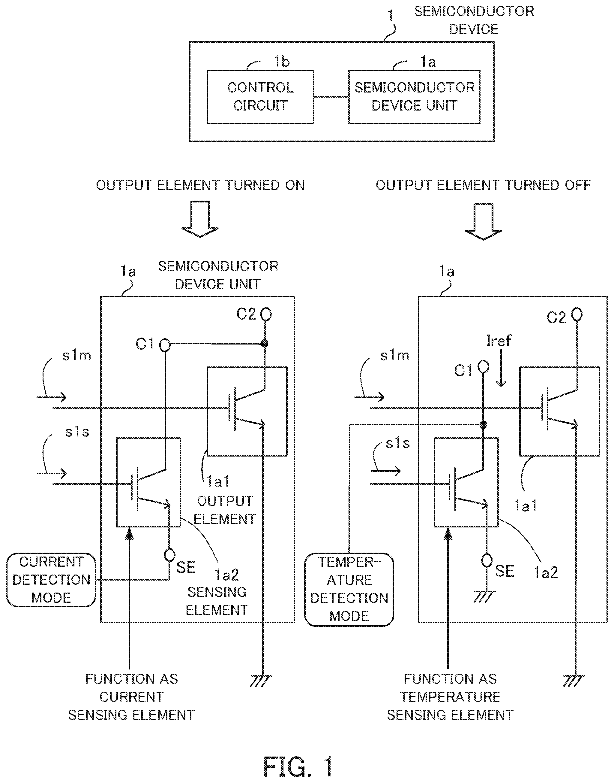
depicts one example of a semiconductor device. A semiconductor device 1 includes a semiconductor device unit 1 a and a control circuit 1 b . The semiconductor device unit 1 a includes an output element 1 a 1 and a sensing element 1 a 2 .
As one example, the output element 1 a 1 is a voltage-controlled power semiconductor element, such as an IGBT or a metal-oxide-semiconductor field-effect transistor (MOSFET), and performs switching based on a driving signal s 1 m outputted from the control circuit 1 b to operate a load. The sensing element 1 a 2 is for example a sensing IGBT, and is switched and driven based on a driving signal s 1 s outputted from the control circuit 1 b.
In this configuration, the control circuit 1 b enters a current detection mode when the output element 1 a 1 is turned on. As one example, the output element 1 a 1 is turned on when the driving signal s 1 m is outputted at an H-level.
In this case, the control circuit 1 b connects a high potential terminal C 1 (or “first high potential terminal) of the sensing element 1 a 2 to a high potential terminal C 2 (or “second high potential terminal”) of the output element 1 a 1 and ungrounds a low potential terminal SE of the sensing element 1 a 2 . The control circuit 1 b then turns on the sensing element 1 a 2 using the driving signal s 1 s and drives the sensing element 1 a 2 (as one example, the control circuit 1 b outputs the driving signal s 1 s at an H level) to cause the sensing element 1 a 2 to function as a current sensing element for detecting the current flowing through the output element 1 a 1 .
The control circuit 1 b enters a temperature detection mode when the output element 1 a 1 is turned off. As one example, when the driving signal s 1 m is outputted at an L level, the output element 1 a 1 is turned off.
In this case, the control circuit 1 b cuts off the connection between the high potential terminal C 1 of the sensing element 1 a 2 and the high potential terminal C 2 of the output element 1 a 1 , supplies a constant current Iref to the high potential terminal C 1 , and grounds the low potential terminal SE of the sensing element 1 a 2 . The control circuit 1 b then turns on and drives the sensing element 1 a 2 using the driving signal s 1 s , which causes the sensing element 1 a 2 to function as a temperature sensing element for detecting the temperature of the output element 1 a 1 .
In this way, the semiconductor device 1 is configured so that the control circuit 1 b causes the sensing element 1 a 2 to function as a current sensing element or as a temperature sensing element based on whether the output element 1 a 1 is turned on or turned off.
By doing so, it is possible to use the same sensing element 1 a 2 to switch between both current detection and temperature detection for the output element 1 a 1 in keeping with the switching state of the output element 1 a 1 . Unlike a conventional configuration, this eliminates the need for a temperature detection diode that is dedicated to detecting temperature, and makes it possible to simplify the manufacturing process and reduce the chip area.
Next, before describing the semiconductor device 1 according to the present disclosure in detail, a semiconductor device that uses a temperature detection diode will be described with reference to . depicts an example configuration of a semiconductor device that uses a temperature detection diode. The semiconductor device 100 includes an IGBT chip 110 and a control circuit 120 . The IGBT chip 110 includes a main IGBT 111 , a sensing IGBT 112 , and a temperature detection diode DI. The control circuit 120 includes a driving circuit 121 , a temperature detection circuit 122 , a current detection circuit 123 , a protection circuit 124 , a constant current source IR, and a sensing resistor Rs.
In the IGBT chip 110 , the main IGBT 111 operates a load by switching based on a driving signal s 11 . Note that a load (not illustrated) may be connected between the emitter of the main IGBT 111 and ground (GND). The sensing IGBT 112 is a power semiconductor element for current-sensing that generates a sensing current Is, which is proportional to the collector current Ic flowing through the main IGBT 111 . The temperature detection diode DI is provided in the vicinity of the main IGBT 111 as an element for detecting the temperature of the main IGBT 111 .
A collector electrode C is connected to the collector of the main IGBT 111 and the collector of the sensing IGBT 112 . The gate of the main IGBT 111 is connected to the gate of the sensing IGBT 112 and an output end of the driving circuit 121 . The main emitter of the main IGBT 111 is connected to GND. A sensing emitter of the sensing IGBT 112 is connected to an input end of the current detection circuit 123 and one end of the sensing resistor Rs. The other end of the sensing resistor Rs is connected to GND.
The anode of the temperature detection diode DI is connected to the input end of the temperature detection circuit 122 and the output end of the constant current source IR. The cathode of the temperature detection diode DI is connected to GND.
In the control circuit 120 , the driving circuit 121 generates a driving signal s 11 for driving the main IGBT 111 based on a driving control signal s 0 transmitted via an input terminal In. A power supply voltage Vcc is applied to the constant current source IR, which outputs the constant current Iref.
The temperature detection circuit 122 detects an overheating state of the main IGBT 111 . When doing so, the potential generated when the constant current Iref outputted from the constant current source IR flows through the temperature detection diode DI is inputted into the temperature detection circuit 122 as a temperature detection voltage Vdi. The temperature detection circuit 122 detects the temperature state of the main IGBT 111 based on this temperature detection voltage Vdi, and outputs an overheating detection signal s 12 when the temperature state of the main IGBT 111 is detected as being an overheating state.
The current detection circuit 123 detects an overcurrent state of the main IGBT 111 . When doing so, once the main IGBT 111 has been turned on based on the driving signal s 11 , the sensing IGBT 112 is also turned on and the sensing current Is is outputted from the sensing emitter of the sensing IGBT 112 .
The sensing current Is outputted from the sensing IGBT 112 is inputted into the control circuit 120 . The potential generated when this sensing current Is flows through the sensing resistor Rs is inputted into the current detection circuit 123 as a sensing voltage Vs. The current detection circuit 123 detects the current state of the main IGBT 111 based on this sensing voltage Vs, and outputs an overcurrent detection signal s 13 when the current state has been detected as being an overcurrent state.
When the protection circuit 124 has received at least one of the overheating detection signal s 12 and the overcurrent detection signal s 13 , the protection circuit 124 outputs a driving stop signal s 14 to the driving circuit 121 . When the driving circuit 121 has received this driving stop signal s 14 , the driving circuit 121 turns off the main IGBT 111 and thereby stops driving the main IGBT 111 .
depicts the temperature characteristics of a temperature detection diode. The vertical axis indicates the temperature detection voltage Vdi and the horizontal axis indicates the temperature. The temperature detection diode DI has a negative temperature characteristic where the temperature detection voltage Vdi decreases as the temperature rises.
Accordingly, the temperature detection voltage Vdi (a forward voltage) at the anode of the temperature detection diode DI, which is based on the constant current Iref that flows from the constant current source IR toward the temperature detection diode DI, will decrease as the temperature rises. For this reason, the temperature detection circuit 122 detects that the temperature state of the main IGBT 111 is the overheating state when the temperature detection voltage Vdi becomes equal to or lower than a reference voltage.
In the semiconductor device 100 described above, the sensing IGBT 112 incorporated into the IGBT chip 110 is used to detect the current flowing through the main IGBT 111 , and the temperature detection diode DI incorporated into the IGBT chip 110 is used to detect the temperature at the main IGBT 111 . In this way, the IGBT chip 110 uses separate elements for current detection and temperature detection, and has a built-in temperature detection diode DI for detecting temperature. Conversely, by using a configuration that enables detection of temperature and current with a single sensing element, the present disclosure provides a semiconductor device that simplifies the manufacturing process and reduces the chip area.
Next, the configuration and operation of the semiconductor device 1 according to the present disclosure will be described in detail. depicts an example configuration of a semiconductor device. As one example, the semiconductor device 10 is applied to an IPM, and includes an IGBT chip 11 and a control circuit 12 . The IGBT chip 11 corresponds to the semiconductor device unit 1 a in , and the control circuit 12 corresponds to the control circuit 1 b in .
The IGBT chip 11 includes a main IGBT 11 m , a sensing IGBT 11 s , and a switch sw 3 (or “third switch”). The control circuit 12 includes a gate driving circuit (for the main IGBT) 12 m , a gate driving circuit (for the sensing IGBT) 12 s , a temperature detection circuit 12 b , a current detection circuit 12 c , an alarm output/protection circuit 12 d , a logic circuit 12 e , a switch sw 1 (or “first switch”), a switch sw 2 (or “second switch”), a constant current source IR, and a sensing resistor Rs.
The temperature detection circuit 12 b includes a comparator cmp 1 and a reference voltage source that outputs a reference voltage Voh for temperature detection, and inputs the reference voltage Voh into a non-inverting input terminal (+) of the comparator cmp 1 . The current detection circuit 12 c includes a comparator cmp 2 and a reference voltage source that outputs a reference voltage Voc for current detection, and inputs the reference voltage Voc into the inverting input terminal (−) of the comparator cmp 2 .
Out of the switches sw 1 , sw 2 , and sw 3 , a first terminal a 1 of the switch sw 1 is connected to a first terminal a 3 of the switch sw 3 , the collector of the sensing IGBT 11 s , and the inverting input terminal (−) of the comparator cmp 1 . A second terminal b 1 of the switch sw 1 is connected to an output end of the constant current source IR. A power supply voltage Vcc is applied to the input terminal of the constant current source IR.
The first terminal a 2 of the switch sw 2 is connected to GND. A second terminal b 2 of the switch sw 2 is connected to the sensing emitter of the sensing IGBT 11 s , one end of the sensing resistor Rs, and the non-inverting input terminal (+) of the comparator cmp 2 . A second terminal b 3 of the switch sw 3 is connected to the collector electrode C and the collector of the main IGBT 11 m . Note that the main emitter of the main IGBT 11 m and the other end of the sensing resistor Rs are connected to GND.
Here, the gate driving circuit 12 m generates a driving signal s 1 m , which turns the main IGBT 11 m on and off, based on the driving control signal V MIN transmitted for example from a microcomputer via an input terminal In 1 . The gate driving circuit 12 m outputs this driving signal s 1 m to the gate of the main IGBT 11 m to switch the main IGBT 11 m . As one example, when the driving signal s 1 m is at an H level, the main IGBT 11 m is turned on, and when the driving signal s 1 m is at an L level, the main IGBT 11 m is turned off.
The logic circuit 12 e outputs a driving control signal V SIN for driving the sensing IGBT 11 s based on the driving control signal V MIN and a temperature detection control signal s 2 transmitted for example from a microcomputer via an input terminal In 2 .
Based on the driving control signal V MIN and the temperature detection control signal s 2 , the logic circuit 12 e additionally generates and outputs a switching control signal sc 1 (or “first switching control signal”), a switching control signal sc 2 (or “second switching control signal”), and a switching control signal sc 3 (or “third switching control signal”) for respectively switching the switches sw 1 , sw 2 , and sw 3 on and off. Note that the internal configuration of the logic circuit 12 e will be described later with reference to .
The gate driving circuit 12 s generates a driving signal s 1 s for turning the sensing IGBT 11 s on and off based on the driving control signal V SIN (or “sensing element driving control signal”) outputted from the logic circuit 12 e , and outputs this driving signal s 1 s to the gate of the sensing IGBT 11 s to switch the sensing IGBT 11 s . As one example, when the driving signal s 1 s is at an H level, the sensing IGBT 11 s is turned on, and when the driving signal s 1 s is at an L level, the sensing IGBT 11 s is turned off.
(Switching Control)
depicts a switching operation of a switch. Table Ta indicates the correspondence between the operation mode, on and off states of the main IGBT and sensing IGBT, the level of the temperature detection control signal s 2 , the level of the driving control signal V MIN , the level of the driving control signal V SIN , and the switching states (that is, the on/off states) of the switches sw 1 , sw 2 , and sw 3 .
[Current Detection Mode] The driving control signal V MIN is turned on and becomes the H level, which turns on the main IGBT 11 m . The temperature detection control signal s 2 becomes the L level, which turns off the temperature detection mode. When the logic circuit 12 e receives the driving control signal V MIN at the H level and the temperature detection control signal s 2 at the L level, the driving control signal V SIN is turned on and becomes the H level, which turns on the sensing IGBT 11 s.
When the main IGBT 11 m and the sensing IGBT 11 s are both turned on, the switching control terminals of the switches sw 1 and sw 2 receive the switching control signals sc 1 and sc 2 outputted from the logic circuit 12 e , respectively, and are turned off, and the switching control terminal of the switch sw 3 receives the switching control signal sc 3 outputted from the logic circuit 12 e and is turned on. With the switches in this state, the sensing IGBT 11 s functions as a current sensing element and the control circuit 12 enters the current detection mode.
[Temperature Detection Mode] The driving control signal V MIN is turned off and becomes the L level, which turns off the main IGBT 11 m . In addition, the temperature detection control signal s 2 becomes the H level, which turns on the temperature detection mode. When the logic circuit 12 e receives the driving control signal V MIN at the L level and the temperature detection control signal s 2 at the H level, the driving control signal V SIN is turned on and becomes the H level, which turns on the sensing IGBT 11 s.
When the main IGBT 11 m is turned off and the sensing IGBT 11 s is turned on, the switching control terminals of the switches sw 1 and sw 2 receive the switching control signals sc 1 and sc 2 outputted from the logic circuit 12 e , respectively and are both turned on. In addition, the switching control terminal of the switch sw 3 receives the switching control signal sc 3 outputted from the logic circuit 12 e and is turned off. With the switches in this state, the sensing IGBT 11 s functions as a temperature sensing element and the control circuit 12 enters the temperature detection mode.
(Current Detection Mode)
depicts the configuration of a semiconductor device in a switching state during the current detection mode. In the current detection mode, as described above, the switch sw 1 is off, the switch sw 2 is off, and the switch sw 3 is on.
When the switch sw 1 is turned off, the output end of the constant current source IR and the collector (or “first high potential terminal”) of the sensing IGBT 11 s are disconnected. When the switch sw 2 is turned off, the sensing emitter (or “low potential terminal”) of the sensing IGBT 11 s becomes ungrounded. When the switch sw 3 is turned on, the collector of the sensing IGBT 11 s and the collector (or “second high potential terminal”) of the main IGBT 11 m are connected.
When the switches are in this state, the sensing current Is outputted from the sensing emitter of the sensing IGBT 11 s flows toward the current detection circuit 12 c . Since one end of the sensing resistor Rs is connected to the non-inverting input terminal (+) of the comparator cmp 2 of the current detection circuit 12 c and the other end of the sensing resistor Rs is connected to GND, the potential generated by the current Is flowing through the sensing resistor Rs is inputted into the comparator cmp 2 as the sensing voltage Vs.
The comparator cmp 2 compares the sensing voltage Vs with the reference voltage Voc used for current detection. When the sensing voltage Vs is equal to or higher than the reference voltage Voc, the comparator cmp 2 detects that the current state of the main IGBT 11 m is an overcurrent state and outputs an overcurrent detection signal s 4 (at the H level).
(Temperature Detection Mode)
depicts the configuration of a semiconductor device in a switching state during a temperature detection mode. In the temperature detection mode, as described above, the switch sw 1 is on, the switch sw 2 is on, and the switch sw 3 is off.
When the switch sw 1 is turned on, the output end of the constant current source IR and the collector of the sensing IGBT 11 s are connected. When the switch sw 2 is turned on, the sensing emitter of the sensing IGBT 11 s is grounded. When the switch sw 3 is turned off, the collector of the sensing IGBT 11 s and the collector of the main IGBT 11 m are disconnected.
With the switches in this state, the constant current Iref outputted from the constant current source IR flows to the sensing IGBT 11 s . The collector-sensing emitter voltage, which is a potential generated at the sensing IGBT 11 s at this time, is inputted into the comparator cmp 1 of the temperature detection circuit 12 b as a temperature detection voltage Vsce indicating the temperature state of the main IGBT 11 m.
The comparator cmp 1 compares the temperature detection voltage Vsce with the reference voltage Voh for temperature detection. On detecting based on the comparison result that the temperature state of the main IGBT 11 m is the overheating state, the comparator cmp 1 outputs an overheating detection signal s 3 (at the H level).
depicts the temperature characteristics of the sensing IGBT. The vertical axis is the temperature detection voltage Vsce and the horizontal axis is the temperature. The sensing IGBT 11 s has a negative temperature characteristic whereby the temperature detection voltage Vsce decreases as the temperature rises.
Accordingly, the temperature detection voltage Vsce between the collector and sensing emitter of the sensing IGBT 11 s , which is based on the constant current Iref flowing from the constant current source IR toward the sensing IGBT 11 s , decreases as the temperature rises. For this reason, when the temperature detection voltage Vsce has become equal to or lower than the reference voltage Voh, the comparator cmp 1 of the temperature detection circuit 12 b detects that the temperature state of the main IGBT 11 m is the overheating state.
(Alarm Output and Protection)
When the alarm output/protection circuit 12 d has received at least one of the overheating detection signal s 3 and the overcurrent detection signal s 4 , the alarm output/protection circuit 12 d outputs an alarm signal s 6 via an output terminal ALM to notify the periphery of an alarm state. When the alarm output/protection circuit 12 d has received at least one of the overheating detection signal s 3 and the overcurrent detection signal s 4 , the alarm output/protection circuit 12 d also outputs a driving stop signal s 5 to the gate driving circuit 12 m . On receiving this driving stop signal s 5 , the gate driving circuit 12 m turns off the main IGBT 11 m and stops driving the main IGBT 11 m.
(Example Configuration of Logic Circuits)
depict example configurations of logic circuits. The logic circuit 12 e includes an RS type flip-flop 12 e 1 and a D type flip-flop 12 e 2 .
At the RS type flip-flop 12 e 1 depicted in , the driving control signal V MIN is inputted into a set terminal (S), and the temperature detection control signal s 2 is inputted into a reset terminal (R). The switching control signal sc 3 is outputted from the output terminal Q, and the output from the inverting output terminal QN is used as the switching control signals sc 1 and sc 2 .
In a truth table T 1 of the RS type flip-flop 12 e 1 of this configuration, when (V MIN , s 2 )=(S, R)=(0, 0), (sc 3 , sc 1 /sc 2 )=(Q, QN)=(hold, hold), so that the output levels are held.
When (V MIN , s 2 )=(S, R)=(0, 1), (sc 3 , sc 1 /sc 2 )=(Q, QN)=(0, 1), which sets the temperature detection mode. That is, since the switching control signal sc 3 is the L level and the switching control signals sc 1 and sc 2 become the H level, the switch sw 3 is turned off and the switches sw 1 and sw 2 are turned on, so that the sensing IGBT 11 s becomes a temperature sensing element and enters the temperature detection mode.
Additionally, when (V MIN , s 2 )=(S, R)=(1, 0), (sc 3 , sc 1 /sc 2 )=(Q, QN)=(1, 0), which sets the current detection mode. That is, since the switching control signal sc 3 becomes the H level and the switching control signals sc 1 and sc 2 become the L level, the switch sw 3 is turned on and the switches sw 1 and sw 2 are turned off, so that the sensing IGBT 11 s becomes a current sensing element and enters the current detection mode.
Note that when (V MIN , s 2 )=(S, R)=(1, 1), (sc 3 , sc 1 /sc 2 )=(Q, QN)=(prohibited, prohibited) (that is, a setting where V MIN =s 2 =H level is not performed).
The RS type flip-flop 12 e 1 includes two-input, one-output NOR elements IC 1 and IC 2 . One terminal of the NOR element IC 1 is used as the reset terminal (R), and one terminal of the NOR element IC 2 is used as the set terminal (S). The output terminal of the NOR element IC 1 is used as the output terminal Q, and the output terminal of the NOR element IC 2 is used as the inverting output terminal QN. The other input terminal of the NOR element IC 1 is connected to the inverting output terminal QN of the NOR element IC 2 , and the other input terminal of the NOR element IC 2 is connected to the output terminal Q of the NOR element IC 1 .
At the D-type flip-flop 12 e 2 depicted in , the driving control signal V MIN is inputted into the clock terminal (CLK), and the temperature detection control signal s 2 is inputted into the input terminal (D). The driving control signal V SIN is outputted from the inverting output terminal QN (the output terminal Q remains unused).
In a truth table T 2 of the D-type flip-flop 12 e 2 , when (V MIN , s 2 )=(CLK, D)=(0, 0), V SIN =QN=hold, so that the output levels are held. When (V MIN , s 2 )=(CLK, D)=(0, 1), V SIN =QN=hold, so that the output levels are held.
When (V MIN , s 2 )=(CLK, D)=(1, 0), V SIN =QN=1, so that the sensing IGBT 11 s is turned on. Note that when (V MIN , s 2 )=(CLK, D)=(1, 1), V SIN =QN=0, but since a setting of V MIN =s 2 =H level is not performed, this logic state is not used.
The D-type flip-flop 12 e 2 includes two-input, one-output NAND elements IC 11 , IC 12 , IC 13 , and IC 14 . One terminal of the NAND element IC 11 is used as an input terminal (D) and one terminal of the NAND element IC 12 is used as the clock terminal (CLK). The output terminal of the NAND element IC 13 is used as the output terminal Q and the output terminal of the NAND element IC 14 is used as the inverting output terminal QN.
The other input terminal of the NAND element IC 11 is connected to the clock terminal (CLK). The other input terminal of the NAND element IC 12 is connected to the output terminal of the NAND element IC 11 and one input terminal of the NAND element IC 13 .
The output terminal of the NAND element IC 12 is connected to one input terminal of the NAND element IC 14 . The other input terminal of the NAND element IC 13 is connected to the inverting output terminal QN of the NAND element IC 14 , and the other input terminal of the NAND element IC 14 is connected to the output terminal Q of the NAND element IC 13 .
(Modification of Semiconductor Device)
depicts a modification of the semiconductor device. In a semiconductor device 10 a , the switch sw 3 is disposed outside an IGBT chip 11 - 1 , but the other configurations are the same as in . The first terminal a 3 of the switch sw 3 is connected via a terminal Csense to the inverting input terminal (−) of the comparator cmp 1 , the first terminal a 1 of the switch sw 1 , and the collector of the sensing IGBT 11 s . The second terminal b 3 of the switch sw 3 is connected to the collector electrode C and via the terminal Cmain to the collector of the main IGBT 11 m.
In this way, by using an external-type configuration where the main IGBT 11 m and the sensing IGBT 11 s are incorporated in the IGBT chip 11 - 1 but the switch sw 3 is disposed outside, it is possible to reduce the circuit scale of the IGBT chip 11 - 1 .
(Application to High-Side Circuit)
depicts an example of a semiconductor device that has been applied to a high-side circuit. Although the semiconductor device 10 described above is configured for a low-side circuit application, a semiconductor device 10 b in has been configured for a high-side circuit application.
In the semiconductor device 10 b , the emitter of the main IGBT 11 m is connected to the first terminal a 2 of the switch sw 2 , the other end of the sensing resistor Rs, the negative terminal of the reference voltage source that outputs the reference voltage Voc, and the negative terminal of the reference voltage source that outputs the reference voltage Voh. Other configurations are the same as in .
As described above, according to the present disclosure, since the sensing element is configured to be capable of both current detection and temperature detection of the output element, a temperature detection diode may be omitted, the manufacturing process is simplified, and there is a further effect of a reduction in chip area.
Although embodiments of the present embodiment have been described above, the configuration of each part indicated in the embodiments may be replaced with other parts with similar functions. As one example, a wide bandgap semiconductor such as silicon carbide (SiC) may be used as the output element. It is also possible to add other optionally chosen components or processes. Any two or more configurations (or features) in the embodiment described above may also be combined into single elements.
According to an aspect of the present disclosure, it is possible to simplify a manufacturing process and to reduce chip area.
All examples and conditional language provided herein are intended for the pedagogical purposes of aiding the reader in understanding the invention and the concepts contributed by the inventor to further the art, and are not to be construed as limitations to such specifically recited examples and conditions, nor does the organization of such examples in the specification relate to a showing of the superiority and inferiority of the invention. Although one or more embodiments of the present invention have been described in detail, it should be understood that various changes, substitutions, and alterations could be made hereto without departing from the spirit and scope of the invention.
Figures (12)
Citations
This patent cites (11)
- US7359172
- US7365559
- US9742389
- US9825555
- US11979017
- US12126330
- US12199526
- US2013/0285732
- US2014/0362490
- US2012-085131
- US2013-219633