Motor Controller and BLDC Motor Comprising the Same
Abstract
A motor controller includes a tap position selection circuit, a micro control unit (MCU), and an inverter circuit. The tap position selection circuit is configured to process a plurality of tap position signals transmit processed tap position signals to the MCU. The MCU is configured to output signals to control the operation of the inverter circuit. The inverter circuit includes an output terminal connected to a plurality of coil windings of a stator module of a motor. The tap position selection circuit includes a plurality of first signal input circuits for motor start and a plurality of second signal input circuits for motor stop; each tap position signal is split into a first part and a second part. The first part is input into one first signal input circuit for motor start and the second part is input into one second signal input circuit for motor stop.
Claims (9)
1. A motor controller, comprising: a tap position selection circuit, a micro control unit (MCU), and an inverter circuit; wherein: the tap position selection circuit is configured to process a plurality of tap position signals transmit processed tap position signals to the MCU; the MCU is configured to output signals to control the operation of the inverter circuit; the inverter circuit comprises an output terminal connected to a plurality of coil windings of a stator module of a motor; the tap position selection circuit comprises a plurality of first signal input circuits for motor start and a plurality of second signal input circuits for motor stop; each tap position signal M is split into a first part and a second part; the first part is input into one first signal input circuit for motor start and the second part is input into one second signal input circuit for motor stop; and the first signal input circuit for motor start and the second signal input circuit for motor stop output two level signals, IO-a and IO-b, respectively, to the MCU, and the MCU controls a start or stop state of the motor based on a magnitude of the two level signals, IO-a and IO-b.
Show 8 dependent claims
2. The motor controller of claim 1 , wherein the first signal input circuit for motor start has a first threshold voltage U 1 , and the second signal input circuit for motor stop has a second threshold voltage U 2 ; a potential difference is present between the first threshold voltage U 1 and the second threshold voltage U 2 ; when a voltage of the tap position signal M is greater than the first threshold voltage U 1 , the level signal IO-a is high-level; when the voltage of the tap position signal M is less than the first threshold voltage U 1 , the level signal IO-a is low-level; similarly, when the voltage of the tap position signal M is greater than the second threshold voltage U 2 , the level signal IO-b is high-level, and when the voltage value of the tap position signal M is less than the second threshold voltage U 2 , the level signal IO-b is low-level.
3. The motor controller of claim 2 , wherein the first signal input circuit for motor start comprises a resistor R 3 , a capacitor C 5 , a diode D 1 , a voltage regulator ZD 1 , a transistor Q 1 , an optocoupler chip U 10 , a capacitor C 1 , and a resistor R 2 ; the tap position signal M is transmitted to a first input pin 1 a of the optocoupler chip U 10 ; the transistor Q 1 comprises a first collector, a first emitter, and a first base; the first collector of the transistor Q 1 is connected to a second input pin 2 a of the optocoupler chip U 10 , and the first emitter of the transistor Q 1 is grounded; one end of the resistor R 3 is in series with one end of the voltage regulator ZD 1 , and the other end of the voltage regulator ZD 1 is connected to the first base of the transistor Q 1 ; the other end of the resistor R 3 is in series with one end of the voltage regulator ZD 1 , and the other end of the voltage regulator ZD 1 is connected to one end of the capacitor C 5 ; the other end of the capacitor C 5 is grounded; the tap position signal M is transmitted to the one end of the capacitor C 5 through the diode D 1 ; the capacitor C 1 and the resistor R 2 are connected in parallel; one end of a parallel combination of the capacitor C 1 and the resistor R 2 is connected to an output pin 3 a of the optocoupler chip U 10 , and the other end of the parallel combination is grounded.
4. The motor controller of claim 3 , wherein a magnitude of the first threshold voltage U 1 is determined by the resistor R 3 and the voltage regulator ZD 1 ; when the diode D 1 receives the tap position signal M, the capacitor C 5 is charged; when a terminal voltage of the capacitor C 5 exceeds the first threshold voltage U 1 , the transistor Q 1 switches on, so that a connection among the first input pin 1 a of the optocoupler chip U 10 , the second input pin 2 a of the optocoupler chip U 10 , and the transistor Q 1 is established, allowing the optocoupler chip U 10 to output the level signal IO-a at high state; when the terminal voltage of the capacitor C 5 is lower than the first threshold voltage U 1 , the transistor Q 1 switches off, and no connection is established among the first input pin 1 a of the optocoupler chip U 10 , the second input pin 2 a of the optocoupler chip U 10 , and the transistor Q 1 ; as a result, the optocoupler chip U 10 outputs the level signal IO-a at low state.
5. The motor controller of claim 4 , wherein the second signal input circuit for motor stop comprises a resistor R 10 , a capacitor C 6 , a diode D 3 , a voltage regulator ZD 2 , a transistor Q 2 , an optocoupler chip U 20 , a capacitor C 3 , and a resistor R 9 ; the tap position signal M is transmitted to the first input pin 1 b of the optocoupler chip U 20 ; the transistor Q 2 comprises a second collector, a second emitter, and a second base; the second collector of the transistor Q 2 is connected to the second input pin 2 b of the optocoupler chip U 20 , and the second emitter of the transistor Q 2 is grounded; one end of the resistor R 10 is in series with one end of the voltage regulator ZD 2 , and the other end of the voltage regulator ZD 2 is connected to the second base of the transistor Q 2 ; the other end of the resistor R 10 is connected to one end of the capacitor C 6 , and the other end of the capacitor C 6 is grounded; the tap position signal M is transmitted to the one end of the capacitor C 6 through the diode D 3 ; the capacitor C 3 and the resistor R 9 are connected in parallel; one end of the parallel combination is connected to the output pin 3 b of the optocoupler chip U 20 , and the other end of the parallel combination is grounded.
6. The motor controller of claim 5 , wherein a magnitude of the second threshold voltage U 2 is determined by the resistor R 10 and the voltage regulator ZD 2 ; when the diode D 3 receives the tap position signal M, the capacitor C 6 is charged; when a terminal voltage of the capacitor C 6 exceeds the second threshold voltage U 2 , the transistor Q 2 switches on, so that a connection among the first input pin 1 b of the optocoupler chip U 20 , the second input pin 2 b of the optocoupler chip U 20 , and the transistor Q 2 is established, allowing the optocoupler chip U 20 to output the level signal IO-b at high state; when the terminal voltage of the capacitor C 6 is lower than the second threshold voltage U 2 , the transistor Q 2 switches off, and no connection is established among the first input pin 1 b of the optocoupler chip U 20 , the second input pin 2 b of the optocoupler chip U 20 , and the transistor Q 2 ; as a result, the optocoupler chip U 20 outputs the level signal IO-b at low state.
7. The motor controller of claim 6 , wherein the first threshold voltage U 1 is greater than the second threshold voltage U 2 .
8. The motor controller of claim 7 , wherein the plurality of tap position signals comprise two tap position signals, M 1 and M 2 .
9. A brushless direct current (BLDC) motor, comprising a motor and the motor controller of claim 1 , and the motor comprising a stator, a rotor, and a housing.
Full Description
Show full text →
CROSS-REFERENCE TO RELAYED APPLICATIONS
This application is a continuation-in-part of International Patent Application No. PCT/CN2022/079834 with an international filing date of Mar. 9, 2022, designating the United States, now pending, and further claims foreign priority benefits to Chinese Patent Application No. 202121881887.1 filed Aug. 12, 2021. The contents of all of the aforementioned applications, including any intervening amendments thereto, are incorporated herein by reference. Inquiries from the public to applicants or assignees concerning this document or the related applications should be directed to: Matthias Scholl P C., Attn.: Dr. Matthias Scholl Esq., 245 First Street, 18th Floor, Cambridge, MA 02142.
BACKGROUND
The disclosure relates to a motor controller and a brushless direct current (BLDC) motor comprising the same.
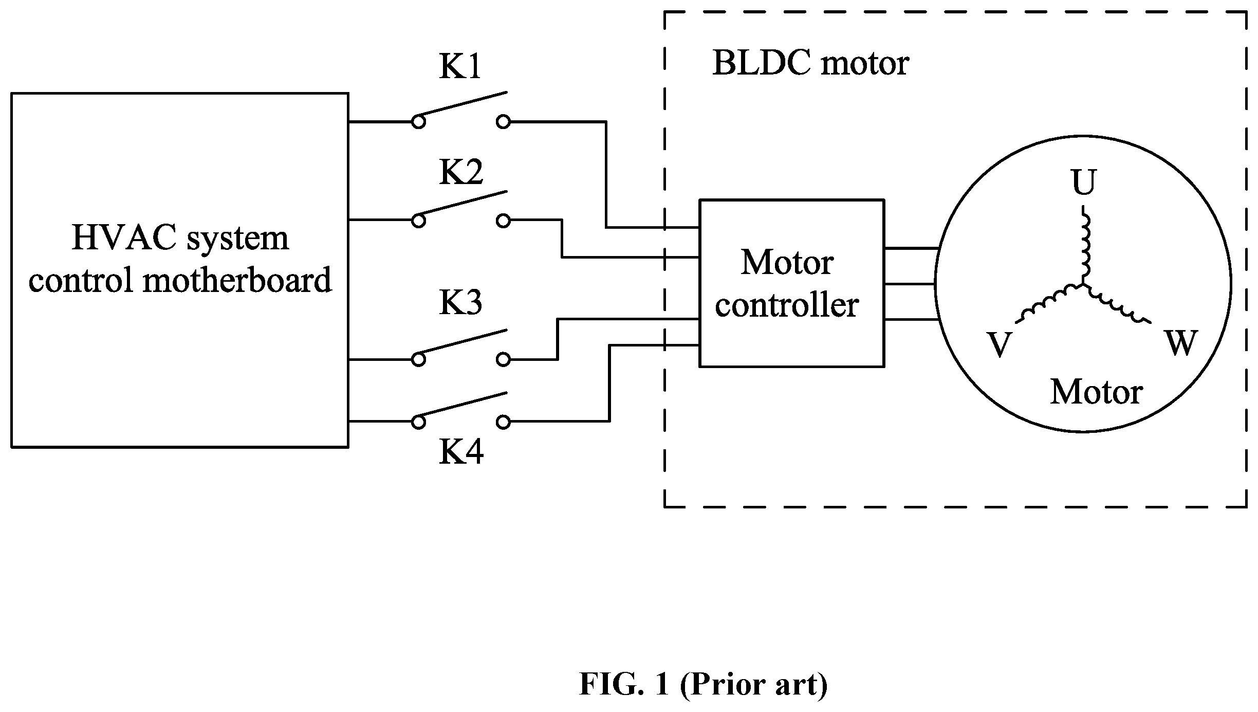
As shown in , a conventional HVAC system (i.e., heating, ventilation, and air conditioning system) includes a mainboard that receives multiple relay signals (0-24 VAC) to control the operation of the BLDC motor in different modes such as heating, cooling, ventilation, dehumidification, etc. A 24 VAC signal is susceptible to fluctuations or interference of power grids. In severe instances, the fluctuations and inference may prevent the activation of the intended mode or mistakenly trigger an incorrect mode, resulting in the disability of air conditioning functionality.
SUMMARY
To solve the aforesaid problems, the first objective of the disclosure is to provide a motor controller.
The motor controller comprises a tap position selection circuit, a micro control unit (MCU), and an inverter circuit. The tap position selection circuit is configured to process a plurality of tap position signals transmit processed tap position signals to the MCU; the MCU is configured to output signals to control the operation of the inverter circuit; the inverter circuit comprises an output terminal connected to a plurality of coil windings of a stator module of a motor; the tap position selection circuit comprises a plurality of first signal input circuits for motor start and a plurality of second signal input circuits for motor stop; each tap position signal M is split into a first part and a second part; the first part is input into one first signal input circuit for motor start and the second part is input into one second signal input circuit for motor stop; and the first signal input circuit for motor start and the second signal input circuit for motor stop output two level signals, IO-a and IO-b, respectively, to the MCU, and the MCU controls a start or stop state of the motor based on a magnitude of the two level signals, IO-a and IO-b.
In a class of this embodiment, the first signal input circuit for motor start has a first threshold voltage U 1 , and the second signal input circuit for motor stop has a second threshold voltage U 2 ; a potential difference is present between the first threshold voltage U 1 and the second threshold voltage U 2 . When the voltage of the tap position signal M is greater than the first threshold voltage U 1 , the level signal IO-a is high-level. When the voltage of the tap position signal M is less than the first threshold voltage U 1 , the level signal IO-a is low-level. Similarly, when the voltage of the tap position signal M is greater than the second threshold voltage U 2 , the level signal IO-b is high-level, and when the voltage value of the tap position signal M is less than the second threshold voltage U 2 , the level signal IO-b is low-level.
In a class of this embodiment, the first signal input circuit for motor start comprises a resistor R 3 , a capacitor C 5 , a diode D 1 , a voltage regulator ZD 1 , a transistor Q 1 , an optocoupler chip U 10 , a capacitor C 1 , and a resistor R 2 ; the tap position signal M is transmitted to a first input pin 1 a of the optocoupler chip U 10 ; the transistor Q 1 comprises a first collector, a first emitter, and a first base; the first collector of the transistor Q 1 is connected to a second input pin 2 a of the optocoupler chip U 10 , and the first emitter of the transistor Q 1 is grounded; one end of the resistor R 3 is in series with one end of the voltage regulator ZD 1 , and the other end of the voltage regulator ZD 1 is connected to the first base of the transistor Q 1 ; the other end of the resistor R 3 is in series with one end of the voltage regulator ZD 1 , and the other end of the voltage regulator ZD 1 is connected to one end of the capacitor C 5 ; the other end of the capacitor C 5 is grounded; the tap position signal M is transmitted to the one end of the capacitor C 5 through the diode D 1 ; the capacitor C 1 and the resistor R 2 are connected in parallel; one end of the parallel combination is connected to an output pin 3 a of the optocoupler chip U 10 , and the other end of the parallel combination is grounded.
In a class of this embodiment, a magnitude of the first threshold voltage U 1 is determined by the resistor R 3 and the voltage regulator ZD 1 . When the diode D 1 receives the tap position signal M, the capacitor C 5 is charged. When the terminal voltage of the capacitor C 5 exceeds the first threshold voltage U 1 , the transistor Q 1 switches on, so that a connection among the first input pin 1 a of the optocoupler chip U 10 , the second input pin 2 a of the optocoupler chip U 10 , and the transistor Q 1 is established, allowing the optocoupler chip U 10 to output the level signal IO-a at high state. When the terminal voltage of the capacitor C 5 is lower than the first threshold voltage U 1 , the transistor Q 1 switches off, and no connection is established among the first input pin 1 a of the optocoupler chip U 10 , the second input pin 2 a of the optocoupler chip U 10 , and the transistor Q 1 ; as a result, the optocoupler chip U 10 outputs the level signal IO-a at low state.
In a class of this embodiment, the second signal input circuit for motor stop comprises a resistor R 10 , a capacitor C 6 , a diode D 3 , a voltage regulator ZD 2 , a transistor Q 2 , an optocoupler chip U 20 , a capacitor C 3 , and a resistor R 9 ; the tap position signal M is transmitted to the first input pin 1 b of the optocoupler chip U 20 ; the transistor Q 2 comprises a second collector, a second emitter, and a second base; the second collector of the transistor Q 2 is connected to the second input pin 2 b of the optocoupler chip U 20 , and the second emitter of the transistor Q 2 is grounded; one end of the resistor R 10 is in series with one end of the voltage regulator ZD 2 , and the other end of the voltage regulator ZD 2 is connected to the second base of the transistor Q 2 ; the other end of the resistor R 10 is connected to one end of the capacitor C 6 , and the other end of the capacitor C 6 is grounded; the tap position signal M is transmitted to the one end of the capacitor C 6 through the diode D 3 ; the capacitor C 3 and the resistor R 9 are connected in parallel; one end of the parallel combination is connected to the output pin 3 b of the optocoupler chip U 20 , and the other end of the parallel combination is grounded.
In a class of this embodiment, the magnitude of the second threshold voltage U 2 is determined by the resistor R 10 and the voltage regulator ZD 2 . When the diode D 3 receives the tap position signal M, the capacitor C 6 is charged. When the terminal voltage of the capacitor C 6 exceeds the second threshold voltage U 2 , the transistor Q 2 switches on, so that a connection among the first input pin 1 b of the optocoupler chip U 20 , the second input pin 2 b of the optocoupler chip U 20 , and the transistor Q 2 is established, allowing the optocoupler chip U 20 to output the level signal IO-b at high state. When the terminal voltage of the capacitor C 6 is lower than the second threshold voltage U 2 , the transistor Q 2 switches off, and no connection is established among the first input pin 1 b of the optocoupler chip U 20 , the second input pin 2 b of the optocoupler chip U 20 , and the transistor Q 2 ; as a result, the optocoupler chip U 20 outputs the level signal IO-b at low state.
In a class of this embodiment, the first threshold voltage U 1 is greater than the second threshold voltage U 2 .
In a class of this embodiment, the tap position signals comprise two tap position signals, M 1 and M 2 .
The second objective of the disclosure is to provide a BLDC motor; the BLDC motor comprises a motor and the motor controller; the motor comprises a stator, a rotor, and a housing.
The following advantages are associated with the disclosure.
Each tap position signal M is split and input into one of the first signal input circuits for motor start and one of the second signal input circuits for motor stop. Subsequently, the first signal input circuit for motor start and the second signal input circuit for motor stop output two level signals, IO-a and IO-b, respectively. The first signal input circuit for motor start has a first threshold voltage U 1 , and the second signal input circuit for motor stop has a second threshold voltage U 2 . A potential difference is present between the first threshold voltage U 1 and the second threshold voltage U 2 . The MCU controls the start or stop state of the motor based on the magnitude of the two level signals, IO-a and IO-b. Due to a hysteresis potential difference between the first threshold voltage U 1 and U 2 , a hysteresis voltage is present for switching the motor between ON and OFF states, thereby enhancing the anti-interference capability of the motor controller. The MCU monitors the level status of two IO ports corresponding to each tap position signal, so as to determine a voltage range within which the actual voltage value of each tap position signal falls. The monitoring process allows for precise control of the motor controller, ensuring accurate starting and stopping at a voltage threshold. As a result, the overall reliability of the motor controller is improved.
BRIEF DESCRIPTION OF THE DRAWINGS
is a block diagram of a connection between a HVAC system between a BLDC motor in the related art;
is a block diagram of a principle according to Example 1 of the disclosure;
is a block diagram of a tap position selection circuit applied with one tap position signal according to Example 1 of the disclosure;
is a circuit diagram corresponding to the tap position selection circuit ;
is a circuit diagram of an optocoupler chip in ; and
is a circuit block diagram according to Example 2 of the disclosure.
DETAILED DESCRIPTION
To further illustrate the disclosure, embodiments detailing a motor controller and a BLDC motor comprising the same are described below. It should be noted that the following embodiments are intended to describe and not to limit the disclosure.
Example 1
As shown in , 3 , 4 , and 5 , the example provides a motor controller for controlling the operation of a motor. The motor controller comprises a tap position selection circuit, a micro control unit (MCU), and an inverter circuit. Tap position signals are processed by the tap position selection circuit and transmitted to the MCU. The MCU is configured to output signals to control the operation of the inverter circuit. The motor comprises a stator module wrapped with a plurality of coil windings. The inverter circuit comprises an output terminal connected to the plurality of coil windings. Specifically, the tap position selection circuit comprises a plurality of first signal input circuits for motor start and a plurality of second signal input circuits for motor stop. Each tap position signal M is split and input into one first signal input circuit for motor start and one second signal input circuit for motor stop. Subsequently, the first signal input circuit for motor start and the second signal input circuit for motor stop output two level signals, IO-a and IO-b, respectively, to the MCU. The MCU controls the start or stop state of the motor based on the magnitude of the two level signals, IO-a and IO-b.
The first signal input circuit for motor start has a first threshold voltage U 1 , and the second signal input circuit for motor stop has a second threshold voltage U 2 . A potential difference is present between the first threshold voltage U 1 and the second threshold voltage U 2 . When the voltage of the tap position signal M is greater than the first threshold voltage U 1 , the level signal IO-a is high-level. When the voltage of the tap position signal M is less than the first threshold voltage U 1 , the level signal IO-a is low-level. Similarly, when the voltage of the tap position signal M is greater than the second threshold voltage U 2 , the level signal IO-b is high-level, and when the voltage value of the tap position signal M is less than the second threshold voltage U 2 , the level signal IO-b is low-level.
The first signal input circuit for motor start comprises a resistor R 3 , a capacitor C 5 , a diode D 1 , a voltage regulator ZD 1 , a transistor Q 1 , an optocoupler chip U 10 , a capacitor C 1 , and a resistor R 2 . The tap position signal M is transmitted to the first input pin 1 a of the optocoupler chip U 10 . The transistor Q 1 comprises a collector, an emitter, and a base. The collector of the transistor Q 1 is connected to the second input pin 2 a of the optocoupler chip U 10 , and the emitter of the transistor Q 1 is grounded. One end of the resistor R 3 is in series with one end of the voltage regulator ZD 1 , and the other end of the voltage regulator ZD 1 is connected to the base of transistor Q 1 . The other end of resistor R 3 is in series with one end of the voltage regulator ZD 1 , and the other end of the voltage regulator ZD 1 is connected to one end of the capacitor C 5 . The other end of the capacitor C 5 is grounded. The tap position signal M is transmitted to the one end of the capacitor C 5 through the diode D 1 . The capacitor C 1 and the resistor R 2 are connected in parallel. One end of the parallel combination is connected to the output pin 3 a of the optocoupler chip U 10 , and the other end of the parallel combination is grounded.
A magnitude of the first threshold voltage U 1 is determined by the resistor R 3 and the voltage regulator ZD 1 . When the diode D 1 receives the tap position signal M, the capacitor C 5 is charged. When the terminal voltage of the capacitor C 5 exceeds the first threshold voltage U 1 , the transistor Q 1 switches on, so that a connection among the first input pin 1 a of the optocoupler chip U 10 , the second input pin 2 a of the optocoupler chip U 10 , and the transistor Q 1 is established, allowing the optocoupler chip U 10 to output the level signal IO-a at high state. When the terminal voltage of the capacitor C 5 is lower than the first threshold voltage U 1 , the transistor Q 1 switches off, and no connection is established among the first input pin 1 a of the optocoupler chip U 10 , the second input pin 2 a of the optocoupler chip U 10 , and the transistor Q 1 ; as a result, the optocoupler chip U 10 outputs the level signal IO-a at low state.
The second signal input circuit for motor stop comprises a resistor R 10 , a capacitor C 6 , a diode D 3 , a voltage regulator ZD 2 , a transistor Q 2 , an optocoupler chip U 20 , a capacitor C 3 , and a resistor R 9 . The tap position signal M is transmitted to the first input pin 1 b of the optocoupler chip U 20 . The transistor Q 2 comprises a collector, an emitter, and a base. The collector of the transistor Q 2 is connected to the second input pin 2 b of the optocoupler chip U 20 , and the emitter of the transistor Q 2 is grounded. One end of the resistor R 10 is in series with one end of the voltage regulator ZD 2 , and the other end of the voltage regulator ZD 2 is connected to the base of the transistor Q 2 . The other end of the resistor R 10 is connected to one end of the capacitor C 6 , and the other end of the capacitor C 6 is grounded. The tap position signal M is transmitted to the one end of the capacitor C 6 through the diode D 3 . The capacitor C 3 and the resistor R 9 are connected in parallel. One end of the parallel combination is connected to the output pin 3 b of the optocoupler chip U 20 , and the other end of the parallel combination is grounded.
The magnitude of the second threshold voltage U 2 is determined by the resistor R 10 and the voltage regulator ZD 2 . When the diode D 3 receives the tap position signal M, the capacitor C 6 is charged. When the terminal voltage of the capacitor C 6 exceeds the second threshold voltage U 2 , the transistor Q 2 switches on, so that a connection among the first input pin 1 b of the optocoupler chip U 20 , the second input pin 2 b of the optocoupler chip U 20 , and the transistor Q 2 is established, allowing the optocoupler chip U 20 to output the level signal IO-b at high state. When the terminal voltage of the capacitor C 6 is lower than the second threshold voltage U 2 , the transistor Q 2 switches off, and no connection is established among the first input pin 1 b of the optocoupler chip U 20 , the second input pin 2 b of the optocoupler chip U 20 , and the transistor Q 2 ; as a result, the optocoupler chip U 20 outputs the level signal IO-b at low state.
The first threshold voltage U 1 is greater than the second threshold voltage U 2 .
The working principle of the motor controller is as follows: each tap position signal M is split and input into one of the first signal input circuits for motor start and one of the second signal input circuits for motor stop. Subsequently, the first signal input circuit for motor start and the second signal input circuit for motor stop output two level signals, IO-a and IO-b, respectively. The first signal input circuit for motor start has a first threshold voltage U 1 , and the second signal input circuit for motor stop has a second threshold voltage U 2 . A potential difference is present between the first threshold voltage U 1 and the second threshold voltage U 2 . The MCU controls the start or stop state of the motor based on the values of the two level signals, IO-a and IO-b. Due to a hysteresis potential difference between the first threshold voltage U 1 and U 2 , a hysteresis voltage is present for switching the motor between ON and OFF states, thereby enhancing the anti-interference capability of the motor controller.
The MCU monitors the level status of two IO ports corresponding to each tap position signal, so as to determine a voltage range within which the actual voltage value of each tap position signal falls. The monitoring process allows for precise control of the motor controller, ensuring accurate starting and stopping at a voltage threshold. As a result, the overall reliability of the motor controller is improved.
The optocoupler chip U 20 has the same structure as the optocoupler chip U 10 , as shown in .
Example 2
The second example of the monitor controller is an improvement based one Example 1. As shown in , the tap position signals comprise two tap position signals, M 1 and M 2 . The tap position selection circuit comprises two first signal input circuits for motor start and two second signal input circuits for motor stop.
The tap position signal M 1 is applied to one of the two first signal input circuits for motor start and one of the second signal input circuits for motor stop. Subsequently, the first signal input circuit for motor start and the second signal input circuit for motor stop output two level signals, IO 1 and IO 2 , respectively, to two I/O ports of the MCU.
Similarly, the tap position signal M 2 is applied to another first signal input circuit for motor start and another second signal input circuit for motor stop. Subsequently, the another first signal input circuit for motor start and the another second signal input circuit for motor stop output two level signals, IO 3 and IO 4 , respectively, to another two I/O ports of the MCU. Precise start and stop operations of the motor can be achieved by using a truth table in logic as Table 1.
TABLE 1
Level status Level status Level status Level status
Tap position of level signal of level signal of level signal of level signal Voltage
signal status IO1 IO2 IO3 IO4 range
Operation of High level High level Low level Low level Greater than
tap position 12 VAC
signal M1
Operation of Low level Low level High level High level Greater than
tap position 12 VAC
signal M2
Cessation of Low level or Low level Low level Low level Less than 6
tap position high level VAC
signal M1
Cessation of Low level Low level Low level or Low level Less than 6
tap position high level VAC
signal M2
The logical table for the two tap position signals, M 1 and M 2 , is described as follows: when the tap position signal M 1 is greater than 12 VAC, both the level signals IO 1 and IO 2 are high-level; when the tap position signal M 1 is less than 6 VAC, both the level signals IO 1 and IO 2 are low-level; when the tap position signal M 2 is greater than 12 VAC, both the level signals IO 3 and IO 4 are high-level; when the tap position signal M 2 is less than 6 VAC, both the level signals IO 3 and IO 4 are low-level.
1. When both the level signals IO 1 and IO 2 are high-level, the MCU recognizes that the actual voltage of the tap position signal M 1 is above 12 VAC (i.e., threshold voltage U 1 ), indicating the activation of the tap position signal M 1 .
2. When both the level signals IO 1 and IO 2 are low-level, the MCU recognizes that the actual voltage of the tap position signal M 1 is below 6 VAC (i.e., the second threshold voltage U 2 ), indicating the deactivation of the tap position signal M 1 .
3. When the level signal IO 1 is high-level and the level signal IO 2 is low-level, the MCU recognizes that the actual voltage of the tap position signal M 1 is between 6-12 VAC, indicating the deactivation of the tap position signal M 1 .
4. When the level signal IO 1 is low-level and the level signal IO 2 is high-level, the condition is considered invalid.
5. When both the level signals IO 3 and IO 4 are high-level, the MCU recognizes that the actual voltage of the tap position signal M 2 is above 12 VAC, indicating the activation of the tap position signal M 2 .
6. When both the level signals IO 3 and IO 4 are low-level, the MCU recognizes that the actual voltage of the tap position signal M 2 is below 6 VAC, indicating the deactivation of the tap position signal M 2 .
7. When the level signal IO 3 is high-level and the level signal IO 4 is low-level, the MCU recognizes that the actual voltage of the tap position signal M 2 is between 6-12 VAC, indicating the deactivation of the tap position signal M 2 .
8. When the level signal IO 3 is low-level and the level signal IO 4 is high-level, the condition is considered invalid.
Example 3
The example provides a brushless direct current (BLDC) motor; the BLDC motor comprises a motor and the motor controller; the motor comprises a stator, a rotor, and a housing; and the motor controller is one of the motor controllers described in Examples 1-2.
It will be obvious to those skilled in the art that changes and modifications may be made, and therefore, the aim in the appended claims is to cover all such changes and modifications.
Figures (6)
Citations
This patent cites (7)
- US2015/0001021
- US2021/0270363
- US2022/0360085
- US105952889
- US215734083
- US216134439
- US2015033151