Display Device, and Tiled Display Device Including the Display Device
Abstract
A display device includes a substrate including a plurality of emission areas respectively corresponding to a plurality of subpixels for displaying an image, a plurality of light emitting elements respectively located in the plurality of emission areas of a first surface of the substrate and respectively corresponding to the plurality of subpixels, a first planarization layer on the first surface of the substrate and covering the plurality of light emitting elements, and an array layer on the first planarization layer.
Claims (15)
1. A tiled display device comprising: a plurality of display devices arranged parallel to each other; and a seam between the plurality of display devices, wherein a display device of the plurality of display devices comprises: a substrate comprising a plurality of emission areas respectively corresponding to a plurality of subpixels for displaying an image; a plurality of anodes respectively located in portions of the plurality of emission areas of a first surface of the substrate and respectively corresponding to the plurality of subpixels; a plurality of cathodes respectively located in other portions of the plurality of emission areas of the first surface of the substrate and respectively corresponding to the plurality of subpixels; a plurality of light emitting elements on the plurality of anodes and the plurality of cathodes and respectively corresponding to the plurality of subpixels; a first planarization layer on the first surface of the substrate and covering the plurality of anodes, the plurality of cathodes and the plurality of light emitting elements; and an array layer on the first planarization layer, wherein the array layer comprises a plurality of pixel drivers respectively corresponding to the plurality of subpixels, located in a non-emission area between the plurality of emission areas, each of the plurality of pixel drivers comprising at least one transistor, and wherein, in an emission area of the plurality of emission areas, a light emitting element of the plurality of light emitting elements is on an anode of the plurality of anodes and a cathode of the plurality of cathodes and connected to a pixel driver of the plurality of pixel drivers through the anode.
Show 14 dependent claims
2. The tiled display device of claim 1 , wherein a first conductive layer on the first surface of the substrate comprises the plurality of anodes and the plurality of cathodes, wherein the array layer comprises: a first gate insulating layer covering a semiconductor layer on the first planarization layer; a second gate insulating layer covering a second conductive layer on the first gate insulating layer; an interlayer insulating layer covering a third conductive layer on the second gate insulating layer; a second planarization layer covering a fourth conductive layer on the interlayer insulating layer; a third planarization layer covering a fifth conductive layer on the second planarization layer; and a fourth planarization layer covering a sixth conductive layer on the third planarization layer.
3. The tiled display device of claim 2 , wherein the array layer further comprises a plurality of reflective wall structures respectively correspond to edges of the plurality of emission areas, wherein a reflective wall structure of the plurality of reflective wall structures corresponding to an edge of the emission area comprises: a first reflective wall layer in the fourth conductive layer; a first reflective wall hole penetrating the second planarization layer and corresponding to a portion of the first reflective wall layer and the emission area; a second reflective wall layer in the fifth conductive layer, covering the first reflective wall hole, and contacting a portion of the first reflective wall layer through the first reflective wall hole; a second reflective wall hole penetrating the third planarization layer and corresponding to a portion of the second reflective wall layer and the emission area; and a third reflective wall layer in the sixth conductive layer, covering the second reflective wall hole, and contacting a portion of the second reflective wall layer through the second reflective wall hole.
4. The tiled display device of claim 3 , wherein the fourth planarization layer covers the plurality of reflective wall structures, wherein the array layer further comprises: a plurality of light guide holes respectively corresponding to the plurality of emission areas, penetrating the fourth planarization layer, and respectively surrounded by the plurality of reflective wall structures; a plurality of wavelength conversion patterns respectively located in the plurality of light guide holes; a plurality of color filter patterns on the fourth planarization layer and respectively overlapping the plurality of wavelength conversion patterns; and a black matrix on the fourth planarization layer and corresponding to the non-emission area.
5. The tiled display device of claim 4 , wherein the plurality of wavelength conversion patterns overlap the plurality of light emitting elements, respectively, wherein the plurality of emission areas comprise: a first emission area corresponding to a first color having a first wavelength band, a second emission area corresponding to a second color having a second wavelength band lower than that of the first wavelength band, and a third emission area corresponding to a third color having a third wavelength band lower than that of the second wavelength band, wherein the plurality of light emitting elements is configured to emit light of the third color, wherein the plurality of wavelength conversion patterns comprises: a first wavelength conversion pattern corresponding to the first emission area and configured to convert light of the third color emitted from a first light emitting element into light of the first color, a second wavelength conversion pattern corresponding to the second emission area and configured to convert light of the third color emitted from a second light emitting element into light of the second color, and a transmission pattern corresponding to the third emission area and configured to transmit light of the third color emitted from a third light emitting element, and wherein the plurality of color filter patterns comprises: a first color filter pattern corresponding to the first emission area and configured to transmit light of the first color, a second color filter pattern corresponding to the second emission area and configured to transmit light of the second color, and a third color filter pattern corresponding to the third emission area and configured to transmit light of the third color.
6. The tiled display device of claim 4 , wherein the display device further comprises: a first power wiring configured to apply a first power voltage to the plurality of pixel drivers, a second power wiring configured to apply a second power voltage to the plurality of pixel drivers, a third power wiring configured to supply a third power voltage to the plurality of cathodes, a first data wiring configured to apply a first data voltage to the plurality of pixel drivers, and a second data wiring configured to apply a second data voltage to the plurality of pixel drivers, and wherein a pixel driver of the plurality of pixel drivers corresponding to the emission area comprises: a first pixel driving circuit unit configured to generate a control current according to the first data voltage of the first data wiring, a second pixel driving circuit unit configured to generate a driving current supplied to the anode according to the second data voltage of the second data wiring, and a third pixel driving circuit unit configured to control a period during which the driving current is supplied to the anode according to the control current of the first pixel driving circuit unit.
7. The tiled display device of claim 6 , wherein the plurality of subpixels are aligned along a first direction and a second direction intersecting the first direction, wherein the second power wiring comprises: a first wiring pattern in the first conductive layer, corresponding to the non-emission area, and extending in the second direction; a second wiring pattern in the second conductive layer, overlapping the first wiring pattern, and electrically connected to the first wiring pattern through a first power contact hole penetrating the first gate insulating layer and the first planarization layer; a third wiring pattern in the fourth conductive layer, extending in the first direction, and electrically connected to the second wiring pattern through a second power contact hole penetrating the interlayer insulating layer and the second gate insulating layer; and a fourth wiring pattern in the fifth conductive layer, corresponding to the non-emission area, extending in the second direction, overlapping the first wiring pattern, and electrically connected to the third wiring pattern through a third power contact hole penetrating the second planarization layer.
8. The tiled display device of claim 7 , wherein the fourth conductive layer comprises the first power wiring, wherein the fifth conductive layer comprises a power auxiliary pattern spaced from the first data wiring and the second data wiring and electrically connected to the first power wiring through a first power wiring auxiliary contact hole penetrating the second planarization layer.
9. The tiled display device of claim 8 , wherein: the third power wiring comprises the sixth conductive layer; the third reflective wall layer is integrally formed with the third power wiring; and the first reflective wall layer and the second reflective wall layer are electrically connected to the third power wiring through the third reflective wall layer.
10. The tiled display device of claim 9 , wherein: the cathode is electrically connected to the third power wiring through a first cathode auxiliary electrode, a second cathode auxiliary electrode, and a third cathode auxiliary electrode; the second conductive layer comprises the first cathode auxiliary electrode electrically connected to the cathode through a first cathode contact hole penetrating the first gate insulating layer and the first planarization layer; the fourth conductive layer comprises the second cathode auxiliary electrode electrically connected to the first cathode auxiliary electrode through a second cathode contact hole penetrating the interlayer insulating layer and the second gate insulating layer; the fifth conductive layer comprises the third cathode auxiliary electrode electrically connected to the second cathode auxiliary electrode through a third cathode contact hole penetrating the second planarization layer; and the third power wiring is electrically connected to the third cathode auxiliary electrode through a fourth cathode contact hole penetrating the third planarization layer.
11. The tiled display device of claim 6 , wherein the semiconductor layer comprises a channel, a source electrode, and a drain electrode of at least one transistor in the pixel driver, wherein the anode is electrically connected to the pixel driver through a first anode auxiliary electrode and a second anode auxiliary electrode, wherein the second conductive layer comprises the first anode auxiliary electrode electrically connected to the anode through a first anode contact hole penetrating the first gate insulating layer and the first planarization layer, wherein the fourth conductive layer comprises the second anode auxiliary electrode electrically connected to the first anode auxiliary electrode through a second anode contact hole penetrating the interlayer insulating layer and the second gate insulating layer, wherein the second anode auxiliary electrode is electrically connected to a second electrode of a seventeenth transistor through a third anode contact hole and electrically connected to a second electrode of an eighteenth transistor through a fourth anode contact hole, and wherein each of the third anode contact hole and the fourth anode contact hole penetrates the interlayer insulating layer, the second gate insulating layer and the first gate insulating layer.
12. The tiled display device of claim 4 , wherein each of the plurality of light emitting elements is a flip chip-type micro-light emitting diode.
13. The tiled display device of claim 4 , wherein the substrate of the display device comprises glass.
14. The tiled display device of claim 4 , wherein the display device further comprises: pads on a portion of an edge of the first surface of the substrate spaced from the plurality of emission areas; connection wirings on a second surface of the substrate opposite the first surface of the substrate; and side wirings on a side surface between the first surface and the second surface of the substrate and respectively connected between the pads and the connection wirings, wherein the connection wirings are connected to a flexible film through a conductive adhesive member.
15. The tiled display device of claim 4 , wherein the plurality of display devices are arranged in a matrix of M rows and N columns.
Full Description
Show full text →
CROSS-REFERENCE TO RELATED APPLICATIONS
This application is a divisional of U.S. patent application Ser. No. 18/062,927, filed Dec. 7, 2022, which claims priority to and the benefit of Korean Patent Application No. 10-2022-0006592, filed Jan. 17, 2022 and Korean Patent Application No. 10-2022-0060213, filed May 17, 2022, the entire content of all of which is incorporated herein by reference.
BACKGROUND
1. Field
The present disclosure relates to a display device and a tiled display device including the display device.
2. Description of the Related Art
As the information society develops, demands for display devices for displaying images are increasing in various forms. The display devices may be flat panel displays such as liquid crystal displays, field emission displays, and light emitting displays.
The light emitting displays may include an organic light emitting display including an organic light emitting diode element as a light emitting element and a light emitting diode display including an inorganic light emitting diode element such as a light emitting diode (LED) as a light emitting element.
SUMMARY
In the case of the organic light emitting display, the luminance or gray level of light of the organic light emitting diode element is adjusted by adjusting the magnitude of a driving current supplied to the organic light emitting diode element. However, because the wavelength of light emitted from an inorganic light emitting diode element varies according to a driving current, when the inorganic light emitting diode element is driven in the same manner as the organic light emitting diode element, image quality may deteriorate.
Aspects and features of embodiments of the present disclosure provide a display device capable of easily performing a lighting test on a light emitting element and repairing the light emitting element, and a tiled display device including the display device.
However, aspects and features of embodiments of the present disclosure are not restricted to the one set forth herein. The above and other aspects of the present disclosure will become more apparent to one of ordinary skill in the art to which the present disclosure pertains by referencing the detailed description of the present disclosure given below.
According to one or more embodiments a display device includes a substrate including a plurality of emission areas respectively corresponding to a plurality of subpixels for displaying an image, a plurality of light emitting elements respectively located in the plurality of emission areas of a first surface of the substrate and respectively corresponding to the plurality of subpixels, a first planarization layer on the first surface of the substrate and covering the plurality of light emitting elements, and an array layer on the first planarization layer. The array layer includes a plurality of pixel drivers respectively corresponding to the plurality of subpixels, in a non-emission area between the plurality of emission areas, and each of the plurality of pixel drivers including at least one transistor.
The display device further includes a plurality of anodes in respective portions of the plurality of emission areas of the first surface of the substrate and respectively corresponding to the plurality of subpixels, and a plurality of cathodes in other respective portions of the plurality of emission areas of the first surface of the substrate and respectively corresponding to the plurality of subpixels. In an emission area of the plurality of emission areas, a light emitting element of the plurality of light emitting elements is on an anode of the plurality of anodes and a cathode of the plurality of cathodes and connected to a pixel driver through the anode. The first planarization layer further covers the plurality of anodes and the plurality of cathodes.
A first conductive layer on the first surface of the substrate includes the plurality of anodes and the plurality of cathodes. The array layer includes a first gate insulating layer covering a semiconductor layer on the first planarization layer, a second gate insulating layer covering a second conductive layer on the first gate insulating layer, an interlayer insulating layer covering a third conductive layer on the second gate insulating layer, a second planarization layer covering a fourth conductive layer on the interlayer insulating layer, a third planarization layer covering a fifth conductive layer on the second planarization layer, and a fourth planarization layer covering a sixth conductive layer on the third planarization layer.
The array layer further includes a plurality of reflective wall structures respectively corresponding to edges of the emission areas. A reflective wall structure of the plurality of reflective wall structures corresponding to an edge of the emission area comprises a first reflective wall layer in the fourth conductive layer, a first reflective wall hole penetrating the second planarization layer and corresponding to a portion of the first reflective wall layer and the emission area, a second reflective wall layer in the fifth conductive layer, covering the first reflective wall hole, and contacting a portion of the first reflective wall layer through the first reflective wall hole, a second reflective wall hole penetrating the third planarization layer and corresponding to a portion of the second reflective wall layer and the emission area, and a third reflective wall layer in the sixth conductive layer, covering the second reflective wall hole, and contacting a portion of the second reflective wall layer through the second reflective wall hole.
The first reflective wall layer, the second reflective wall layer, and the third reflective wall layer are covered with the fourth planarization layer. The array layer further includes a plurality of light guide holes respectively corresponding to the plurality of emission areas, penetrating the fourth planarization layer, and respectively surrounded by the plurality of reflective wall structures, and a plurality of wavelength conversion patterns respectively located in the plurality of light guide holes. The plurality of wavelength conversion patterns overlap the plurality of light emitting elements, respectively.
The plurality of emission areas include a first emission area corresponding to a first color having a first wavelength band, a second emission area corresponding to a second color having a second band lower than that of the first wavelength band, and a third emission area corresponding to a third color having a third wavelength band lower than that of the second wavelength band. The plurality of light emitting elements is configured to emit light of the third color. The plurality of wavelength conversion patterns include a first wavelength conversion pattern corresponding to the first emission area and configured to convert light of the third color emitted from a first light emitting element of the plurality of light emitting elements into light of the first color, a second wavelength conversion pattern corresponding to the second emission area and configured to convert light of the third color emitted from a second light emitting element of the plurality of light emitting elements into light of the second color, and a transmission pattern corresponding to the third emission area and configured to transmit light of the third color emitted from a third light emitting element of the plurality of light emitting elements.
The array layer further includes a plurality of color filter patterns on the fourth planarization layer and respectively overlapping the plurality of wavelength conversion patterns, and a black matrix on the fourth planarization layer and corresponding to the non-emission area. The plurality of color filter patterns includes a first color filter pattern corresponding to the first emission area and transmitting light of the first color, a second color filter pattern corresponding to the second emission area and transmitting light of the second color, and a third color filter pattern corresponding to the third emission area and transmitting light of the third color.
The array layer further incudes a first power wiring configured to apply a first power voltage to the plurality of pixel drivers, a second power wiring configured to apply a second power voltage to the plurality of pixel drivers, a third power wiring configured to supply a third power voltage to the plurality of cathodes, a scan write wiring configured to transmit a scan write signal to the plurality of pixel drivers, a scan initialization wiring configured to transmit a scan initialization signal to the plurality of pixel drivers, a sweep signal wiring configured to transmit a sweep signal to the plurality of pixel drivers, a first data wiring configured to apply a first data voltage to the plurality of pixel drivers, and a second data wiring configured to applying a second data voltage to the plurality of pixel drivers. A pixel driver of the plurality of pixel drivers corresponding to the emission area includes a first pixel driving circuit unit configured to generate a control current according to the first data voltage of the first data wiring, a second pixel driving circuit unit configured to generate a driving current supplied to the anode according to the second data voltage of the second data wiring, and a third pixel driving circuit unit configured to control a period during which the driving current is supplied to the anode according to the control current of the first pixel driving circuit unit. The first pixel driving circuit unit includes a first transistor configured to generate the control current according to the first data voltage, a second transistor configured to apply the first data voltage of the first data wiring to a first electrode of the first transistor according to the scan write signal, a third transistor configured to apply an initialization voltage of an initialization voltage wiring to a gate electrode of the first transistor according to the scan initialization signal, a fourth transistor connecting the gate electrode of the first transistor and a second electrode of the first transistor according to the scan write signal, and a first capacitor located between the sweep signal wiring and the gate electrode of the first transistor.
The array layer further includes a first emission wiring configured to transmit a first emission signal to the pixel drivers, and a scan control wiring configured to transmit a scan control signal to the pixel drivers. The first pixel driving circuit unit further includes a fifth transistor connecting the first power wiring to the first electrode of the first transistor according to the first emission signal, a sixth transistor connecting the second electrode of the first transistor to the third pixel driving circuit unit according to the first emission signal, and a seventh transistor connecting a first node between the sweep signal wiring and the first capacitor to a gate voltage wiring according to the scan control signal.
The second pixel driving circuit unit includes an eighth transistor configured to generate the driving current according to the second data voltage, a ninth transistor configured to apply the second data voltage of the second data wiring to a first electrode of the eighth transistor according to the scan write signal, a tenth transistor configured to apply the initialization voltage of the initialization voltage wiring to a gate electrode of the eighth transistor according to the scan initialization signal, and an eleventh transistor connecting the gate electrode of the eighth transistor and a second electrode of the eighth transistor according to the scan write signal.
The second pixel driving circuit unit further includes a twelfth transistor connecting the second power wiring to the first electrode of the eighth transistor according to the first emission signal, a thirteenth transistor connecting the first power wiring to a second node according to the scan control signal, a fourteenth transistor connecting the second power wiring to the second node according to the first emission signal, and a second capacitor between the gate electrode of the eighth transistor and the second node.
The array layer further includes a second emission wiring configured to transmit a second emission signal to the pixel drivers, and the third pixel driving circuit unit is connected to the sixth transistor of the first pixel driving circuit unit at a third node. The third pixel driving circuit unit includes a fifteenth transistor having a gate electrode connected to the third node, a sixteenth transistor connecting the third node to the initialization voltage wiring according to the scan control signal, a seventeenth transistor connecting a second electrode of the fifteenth transistor to the anode according to the second emission signal, an eighteenth transistor connecting the anode to the initialization voltage wiring according to the scan control signal, and a third capacitor between the third node and the initialization voltage wiring.
The semiconductor layer includes a channel, a source electrode and a drain electrode of each of the first transistor, the second transistor, the third transistor, the fourth transistor, the fifth transistor, the sixth transistor, the seventh transistor, the eighth transistor, the ninth transistor, the tenth transistor, the eleventh transistor, the twelfth transistor, the thirteenth transistor, the fourteenth transistor, the fifteenth transistor, the sixteenth transistor, the seventeenth transistor and the eighteenth transistor. The second conductive layer includes a gate electrode of each of the first transistor, the second transistor, the third transistor, the fourth transistor, the fifth transistor, the sixth transistor, the seventh transistor, the eighth transistor, the ninth transistor, the tenth transistor, the eleventh transistor, the twelfth transistor, the thirteenth transistor, the fourteenth transistor, the fifteenth transistor, the sixteenth transistor, the seventeenth transistor and the eighteenth transistor, a first capacitor electrode integrally formed with the gate electrode of the first transistor, a second capacitor electrode integrally formed with the gate electrode of the eighth transistor and a third capacitor electrode integrally formed with the gate electrode of the fifteenth transistor. The third conductive layer includes a fourth capacitor electrode overlapping the first capacitor electrode, a fifth capacitor electrode overlapping the second capacitor electrode and a sixth capacitor electrode overlapping the third capacitor electrode.
The subpixels are aligned along a first direction and a second direction intersecting the first direction. The second power wiring includes a first wiring pattern in the first conductive layer, corresponding to the non-emission area, and extending in the second direction, a second wiring pattern in the second conductive layer, overlapping the first wiring pattern, and electrically connected to the first wiring pattern through a first power contact hole penetrating the first gate insulating layer and the first planarization layer, a third wiring pattern in the fourth conductive layer, extending in the first direction, and electrically connected to the second wiring pattern through a second power contact hole penetrating the interlayer insulating layer and the second gate insulating layer, and a fourth wiring pattern in the fifth conductive layer, corresponding to the non-emission area, extending in the second direction, overlapping the first wiring pattern, and electrically connected to the third wiring pattern through a third power contact hole penetrating the second planarization layer.
The fourth conductive layer includes the initialization voltage wiring, the scan initialization wiring, the scan write wiring, the first emission wiring, the second emission wiring, the first power wiring, the sweep signal wiring, the gate voltage wiring and the scan control wiring that extend in the first direction, and are spaced from each other. The fifth conductive layer includes the first data wiring and the second data wiring. The sixth conductive layer includes the third power wiring.
The fifth conductive layer includes a power auxiliary pattern spaced from the first data wiring and the second data wiring, and electrically connected to the first power wiring through a first power wiring auxiliary contact hole penetrating the second planarization layer.
The third reflective wall layer is integrally formed with the third power wiring. The first reflective wall layer and the second reflective wall layer are electrically connected to the third power wiring through the third reflective wall layer.
The cathode is electrically connected to the third power wiring through a first cathode auxiliary electrode, a second cathode auxiliary electrode and a third cathode auxiliary electrode. The second conductive layer includes the first cathode auxiliary electrode electrically connected to the cathode through a first cathode contact hole penetrating the first gate insulating layer and the first planarization layer. The fourth conductive layer includes the second cathode auxiliary electrode electrically connected to the first cathode auxiliary electrode through a second cathode contact hole penetrating the interlayer insulating layer and the second gate insulating layer. The fifth conductive layer includes the third cathode auxiliary electrode electrically connected to the second cathode auxiliary electrode through a third cathode contact hole penetrating the second planarization layer. The third power wiring is electrically connected to the third cathode auxiliary electrode through a fourth cathode contact hole penetrating the third planarization layer.
The anode is electrically connected to the pixel driver through a first anode auxiliary electrode and a second anode auxiliary electrode. The second conductive layer includes the first anode auxiliary electrode electrically connected to the anode through a first anode contact hole penetrating the first gate insulating layer and the first planarization layer. The fourth conductive layer includes the second anode auxiliary electrode electrically connected to the first anode auxiliary electrode through a second anode contact hole penetrating the interlayer insulating layer and the second gate insulating layer. The second anode auxiliary electrode is electrically connected to a second electrode of the seventeenth transistor through a third anode contact hole and electrically connected to a second electrode of the eighteenth transistor through a fourth anode contact hole. Each of the third anode contact hole and the fourth anode contact hole penetrates the interlayer insulating layer, the second gate insulating layer and the first gate insulating layer.
Each of the plurality of light emitting elements includes a flip chip-type micro-light emitting diode.
The substrate includes glass.
The display device further includes pads on a portion of an edge of the first surface of the substrate spaced from the plurality of emission areas, connection wirings on a second surface of the substrate opposite the first surface of the substrate, and side wirings on a side surface between the first surface and the second surface of the substrate and respectively connected between the pads and the connection wirings. The connection wirings are connected to a flexible film through a conductive adhesive member.
According to one or more embodiments, a tiled display device includes a plurality of display devices arranged in parallel to each other, and a seam between the plurality of display devices. A display device of the plurality of display devices includes a substrate including a plurality of emission areas respectively corresponding to a plurality of subpixels for displaying an image, a plurality of anodes respectively located in portions of the plurality of emission areas of a first surface of the substrate and respectively corresponding to the plurality of subpixels, a plurality of cathodes respectively located in other portions of the plurality of emission areas of the first surface of the substrate and respectively corresponding to the plurality of subpixels, a plurality of light emitting elements on the plurality of anodes and the plurality of cathodes and respectively corresponding to the plurality of subpixels, a first planarization layer on the first surface of the substrate and covering the plurality of anodes, the plurality of cathodes and the plurality of light emitting elements, and an array layer on the first planarization layer. The array layer includes a plurality of pixel drivers respectively corresponding to the plurality of subpixels, located in a non-emission area between the plurality of emission areas, each the plurality of pixel drivers including at least one transistor. In an emission area of the plurality of emission areas, a light emitting element of the plurality of light emitting elements is on an anode of the plurality of anodes and a cathode of the plurality of cathodes and connected to a pixel driver of the plurality of pixel drivers through the anode.
A first conductive layer on the first surface of the substrate includes the plurality of anodes and the plurality of cathodes. The array layer includes a first gate insulating layer covering a semiconductor layer on the first planarization layer, a second gate insulating layer covering a second conductive layer on the first gate insulating layer, an interlayer insulating layer covering a third conductive layer on the second gate insulating layer, a second planarization layer covering a fourth conductive layer on the interlayer insulating layer, a third planarization layer covering a fifth conductive layer on the second planarization layer, and a fourth planarization layer covering a sixth conductive layer on the third planarization layer.
The array layer further includes a plurality of reflective wall structures respectively correspond to edges of the plurality of emission areas. A reflective wall structure of the plurality of reflective wall structures corresponding to an edge of the emission area includes a first reflective wall layer in the fourth conductive layer, a first reflective wall hole penetrating the second planarization layer and corresponding to a portion of the first reflective wall layer and the emission area, a second reflective wall layer in the fifth conductive layer, covering the first reflective wall hole, and contacting a portion of the first reflective wall layer through the first reflective wall hole, a second reflective wall hole penetrating the third planarization layer and corresponding to a portion of the second reflective wall layer and the emission area, and a third reflective wall layer in the sixth conductive layer, covering the second reflective wall hole, and contacting a portion of the second reflective wall layer through the second reflective wall hole.
The fourth planarization layer covers the plurality of reflective wall structures. The array layer further includes a plurality of light guide holes respectively corresponding to the plurality of emission areas, penetrating the fourth planarization layer, and respectively surrounded by the plurality of reflective wall structures, a plurality of wavelength conversion patterns respectively located in the plurality of light guide holes, a plurality of color filter patterns on the fourth planarization layer and respectively overlapping the plurality of wavelength conversion patterns, and a black matrix on the fourth planarization layer and corresponding to the non-emission area.
The plurality of wavelength conversion patterns overlap the plurality of light emitting elements, respectively. The plurality of emission areas include a first emission area corresponding to a first color having a first wavelength band, a second emission area corresponding to a second color having a second wavelength band lower than that of the first wavelength band, and a third emission area corresponding to a third color having a third wavelength band lower than that of the second wavelength band. The plurality of light emitting elements is configured to emit light of the third color. The plurality of wavelength conversion patterns include a first wavelength conversion pattern corresponding to the first emission area and configured to convert light of the third color emitted from a first light emitting element into light of the first color, a second wavelength conversion pattern corresponding to the second emission area and configured to convert light of the third color emitted from a second light emitting element into light of the second color, and a transmission pattern corresponding to the third emission area and configured to transmit light of the third color emitted from a third light emitting element. The plurality of color filter patterns include a first color filter pattern corresponding to the first emission area and configured to transmit light of the first color, a second color filter pattern corresponding to the second emission area and configured to transmit light of the second color, and a third color filter pattern corresponding to the third emission area and configured to transmit light of the third color.
The display device further includes a first power wiring configured to apply a first power voltage to the plurality of pixel drivers, a second power wiring configured to apply a second power voltage to the plurality of pixel drivers, a third power wiring configured to supply a third power voltage to the plurality of cathodes, a first data wiring configured to apply a first data voltage to the plurality of pixel drivers, and a second data wiring configured to apply a second data voltage to the plurality of pixel drivers. A pixel driver of the plurality of pixel drivers corresponding to the emission area includes a first pixel driving circuit unit configured to generate a control current according to the first data voltage of the first data wiring, a second pixel driving circuit unit configured to generate a driving current supplied to the anode according to the second data voltage of the second data wiring, and a third pixel driving circuit unit configured to control a period during which the driving current is supplied to the anode according to the control current of the first pixel driving circuit unit.
The plurality of subpixels are aligned along a first direction and a second direction intersecting the first direction. The second power wiring includes a first wiring pattern in the first conductive layer, corresponding to the non-emission area, and extending in the second direction, a second wiring pattern in the second conductive layer, overlapping the first wiring pattern, and electrically connected to the first wiring pattern through a first power contact hole penetrating the first gate insulating layer and the first planarization layer, a third wiring pattern in the fourth conductive layer, extending in the first direction, and electrically connected to the second wiring pattern through a second power contact hole penetrating the interlayer insulating layer and the second gate insulating layer, and a fourth wiring pattern in the fifth conductive layer, corresponding to the non-emission area, extending in the second direction, overlapping the first wiring pattern, and electrically connected to the third wiring pattern through a third power contact hole penetrating the second planarization layer.
The fourth conductive layer includes the first power wiring. The fifth conductive layer includes a power auxiliary pattern spaced from the first data wiring and the second data wiring and electrically connected to the first power wiring through a first power wiring auxiliary contact hole penetrating the second planarization layer.
The third power wiring includes the sixth conductive layer. The third reflective wall layer is integrally formed with the third power wiring. The first reflective wall layer and the second reflective wall layer are electrically connected to the third power wiring through the third reflective wall layer.
The cathode is electrically connected to the third power wiring through a first cathode auxiliary electrode, a second cathode auxiliary electrode and a third cathode auxiliary electrode. The second conductive layer includes the first cathode auxiliary electrode electrically connected to the cathode through a first cathode contact hole penetrating the first gate insulating layer and the first planarization layer. The fourth conductive layer includes the second cathode auxiliary electrode electrically connected to the first cathode auxiliary electrode through a second cathode contact hole penetrating the interlayer insulating layer and the second gate insulating layer. The fifth conductive layer includes the third cathode auxiliary electrode electrically connected to the second cathode auxiliary electrode through a third cathode contact hole penetrating the second planarization layer. The third power wiring is electrically connected to the third cathode auxiliary electrode through a fourth cathode contact hole penetrating the third planarization layer.
The semiconductor layer includes a channel, a source electrode and a drain electrode of at least one transistor in the pixel driver. The anode is electrically connected to the pixel driver through a first anode auxiliary electrode and a second anode auxiliary electrode. The second conductive layer includes the first anode auxiliary electrode electrically connected to the anode through a first anode contact hole penetrating the first gate insulating layer and the first planarization layer. The fourth conductive layer includes the second anode auxiliary electrode electrically connected to the first anode auxiliary electrode through a second anode contact hole penetrating the interlayer insulating layer and the second gate insulating layer. The second anode auxiliary electrode is electrically connected to a second electrode of the seventeenth transistor through a third anode contact hole and electrically connected to a second electrode of the eighteenth transistor through a fourth anode contact hole. Each of the third anode contact hole and the fourth anode contact hole penetrates the interlayer insulating layer, the second gate insulating layer and the first gate insulating layer.
Each of the plurality of light emitting elements includes a flip chip-type micro-light emitting diode.
The substrate of the display device includes glass.
The display device further includes pads on a portion of an edge of the first surface of the substrate spaced from the plurality of emission areas, connection wirings on a second surface of the substrate opposite the first surface of the substrate, and side wirings on a side surface between the first surface and the second surface of the substrate and respectively connected between the pads and the connection wirings. The connection wirings are connected to a flexible film through a conductive adhesive member.
The plurality of display devices are arranged in a matrix of M rows and N columns.
A display device according to one or more embodiments includes a plurality of light emitting elements on a first surface of a substrate, a first planarization layer covering the light emitting elements, and an array layer on the first planarization layer and including a plurality of pixel drivers respectively connected to the light emitting elements.
That is, according to one or more embodiments, because the array layer is on the first planarization layer covering the light emitting elements, it may be placed after the light emitting elements are tested for a lighting defect and repaired. Therefore, a light emitting element having a lighting defect can be easily repaired, thus reducing the influence of a defect rate of the light emitting elements on the display quality of the display device. Accordingly, this may increase the yield and decrease the fabrication cost of the display device. In addition, because the light emitting elements are tested and repaired before the array layer is placed, damage to the array layer due to the test and repair of the light emitting elements can be prevented.
In addition, because the light emitting elements are on the first surface of the substrate rather than on the array layer, misalignment of the light emitting elements due to a step difference of the array layer can be prevented.
However, the effects, aspects, and features of embodiments of the present disclosure are not limited to the aforementioned effects, aspects, and features, and various other effects, aspects, and features are included in the present specification.
BRIEF DESCRIPTION OF THE DRAWINGS
These and/or other aspects will become apparent and more readily appreciated from the following description of the embodiments, taken in conjunction with the accompanying drawings in which:
is a plan view of a display device according to one or more embodiments;
are enlarged layout views of examples of an area A of ;
is a cross-sectional view of an example of a plane cut along the line B-B′ of ;
is a block diagram of the display device according to one or more embodiments;
is an equivalent circuit diagram of an example of any one pixel driver of ;
is a layout view of an example of any one subpixel of ;
is a cross-sectional view of an example of a plane cut along the line C-C′ of ;
is a layout view illustrating a first conductive layer and a light emitting element of ;
is a layout view illustrating the first conductive layer, the light emitting element, a semiconductor layer, a second conductive layer, and a third conductive layer of ;
is a layout view illustrating a fourth conductive layer of ;
is a layout view illustrating the first conductive layer, the light emitting element, the semiconductor layer, the second conductive layer, the third conductive layer, and the fourth conductive layer of ;
is a layout view illustrating a fifth conductive layer of ;
is a layout view illustrating a sixth conductive layer of ;
is a flowchart illustrating a method of fabricating a display device according to one or more embodiments;
is a flowchart illustrating an operation of placing an array layer in ;
through 33 are process diagrams illustrating each operation of ;
is a plan view of a tiled display device according to one or more embodiments;
is an enlarged layout view illustrating the front of portion TD_C of in detail;
is a cross-sectional view of an example of a plane cut along the line I-I′ of ;
is an enlarged layout view illustrating the back of portion TD_B of in detail;
is a cross-sectional view of an example of a plane cut along the line II-II′ of ; and
is a block diagram of the tiled display device according to one or more embodiments.
DETAILED DESCRIPTION
The embodiments will now be described more fully hereinafter with reference to the accompanying drawings. The embodiments may, however, be provided in different forms and should not be construed as limiting. The same reference numbers indicate the same components throughout the disclosure. In the accompanying figures, the thickness of layers and regions may be exaggerated for clarity.
Some of the parts which are not associated with the description may not be provided in order to describe embodiments of the present disclosure.
It will also be understood that when a layer is referred to as being “on” another layer or substrate, it can be directly on the other layer or substrate, or intervening layers may also be present. In contrast, when an element is referred to as being “directly on” another element, there may be no intervening elements present.
Further, the phrase “in a plan view” means when an object portion is viewed from above, and the phrase “in a schematic cross-sectional view” means when a schematic cross-section taken by vertically cutting an object portion is viewed from the side. The terms “overlap” or “overlapped” mean that a first object may be above or below or to a side of a second object, and vice versa. Additionally, the term “overlap” may include layer, stack, face or facing, extending over, covering, or partly covering or any other suitable term as would be appreciated and understood by those of ordinary skill in the art. The expression “not overlap” may include meaning such as “apart from” or “set aside from” or “offset from” and any other suitable equivalents as would be appreciated and understood by those of ordinary skill in the art. The terms “face” and “facing” may mean that a first object may directly or indirectly oppose a second object. In a case in which a third object intervenes between a first and second object, the first and second objects may be understood as being indirectly opposed to one another, although still facing each other.
The spatially relative terms “below,” “beneath,” “lower,” “above,” “upper,” or the like, may be used herein for ease of description to describe the relations between one element or component and another element or component as illustrated in the drawings. It will be understood that the spatially relative terms are intended to encompass different orientations of the device in use or operation, in addition to the orientation depicted in the drawings. For example, in the case where a device illustrated in the drawing is turned over, the device positioned “below” or “beneath” another device may be placed “above” another device. Accordingly, the illustrative term “below” may include both the lower and upper positions. The device may also be oriented in other directions and thus the spatially relative terms may be interpreted differently depending on the orientations.
When an element is referred to as being “connected” or “coupled” to another element, the element may be “directly connected” or “directly coupled” to another element, or “electrically connected” or “electrically coupled” to another element with one or more intervening elements interposed therebetween. It will be further understood that when the terms “comprises,” “comprising,” “has,” “have,” “having,” “includes” and/or “including” are used, they may specify the presence of stated features, integers, steps, operations, elements and/or components, but do not preclude the presence or addition of other features, integers, steps, operations, elements, components, and/or any combination thereof.
It will be understood that, although the terms “first,” “second,” “third,” or the like may be used herein to describe various elements, these elements should not be limited by these terms. These terms are used to distinguish one element from another element or for the convenience of description and explanation thereof. For example, when “a first element” is discussed in the description, it may be termed “a second element” or “a third element,” and “a second element” and “a third element” may be termed in a similar manner without departing from the teachings herein.
The terms “about” or “approximately” as used herein is inclusive of the stated value and means within an acceptable range of deviation for the particular value as determined by one of ordinary skill in the art, considering the measurement in question and the error associated with measurement of the particular quantity (for example, the limitations of the measurement system). For example, “about” may mean within one or more standard deviations, or within ±30%, 20%, 10%, 5% of the stated value.
In the specification and the claims, the term “and/or” is intended to include any combination of the terms “and” and “or” for the purpose of its meaning and interpretation. For example, “A and/or B” may be understood to mean “A, B, or A and B.” The terms “and” and “or” may be used in the conjunctive or disjunctive sense and may be understood to be equivalent to “and/or.” In the specification and the claims, the phrase “at least one of” is intended to include the meaning of “at least one selected from the group of” for the purpose of its meaning and interpretation. For example, “at least one of A and B” may be understood to mean “A, B, or A and B.”
Unless otherwise defined or implied, all terms used herein (including technical and scientific terms) have the same meaning as commonly understood by those skilled in the art to which this disclosure pertains. It will be further understood that terms, such as those defined in commonly used dictionaries, should be interpreted as having a meaning that is consistent with their meaning in the context of the relevant art and will not be interpreted in an ideal or excessively formal sense unless clearly defined in the specification.
Hereinafter, embodiments will be described with reference to the accompanying drawings.
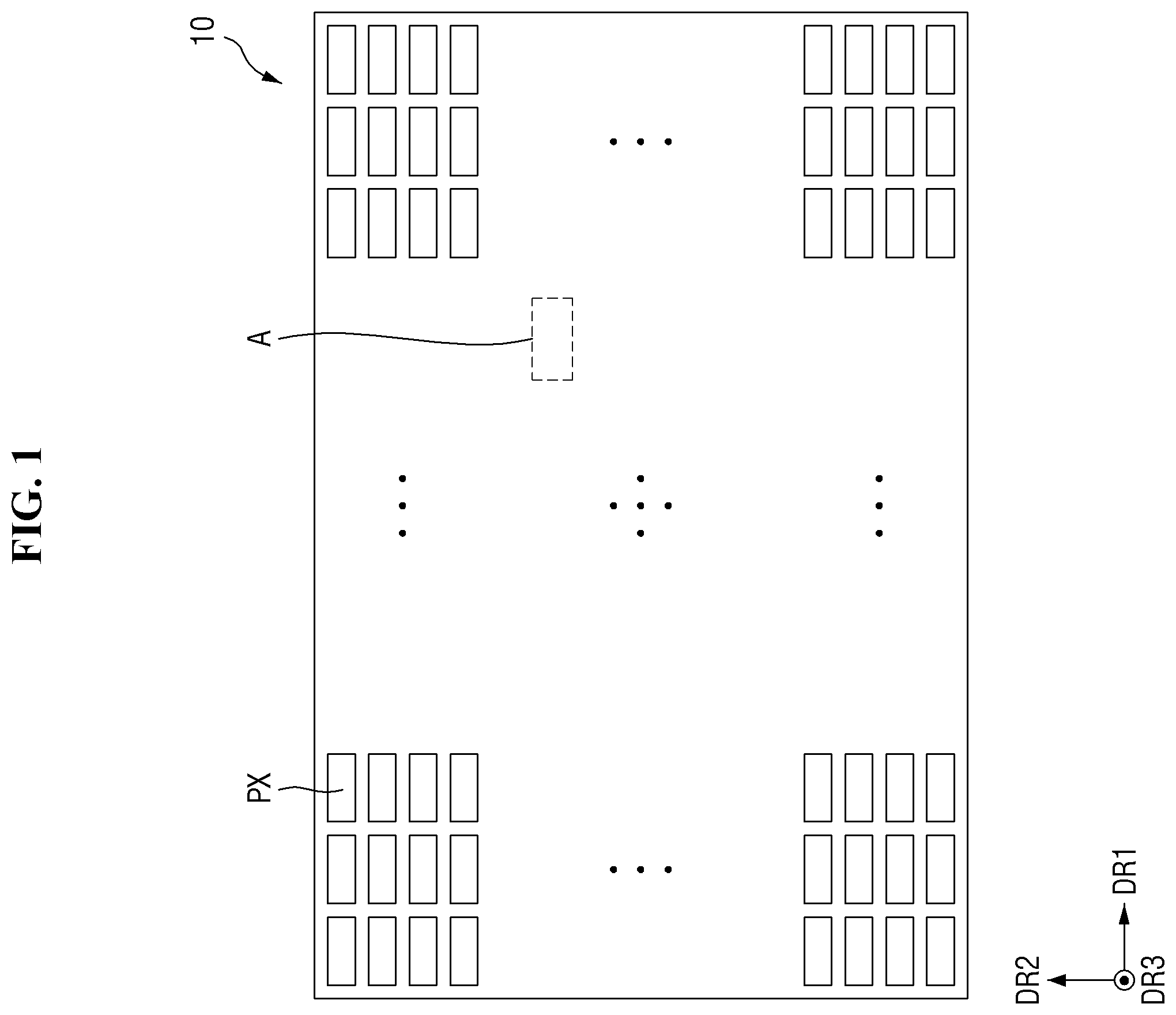
is a plan view of a display device 10 according to one or more embodiments. are enlarged layout views of examples of an area A of .
Referring to , the display device 10 according to one or more embodiments is a device for displaying moving images or still images. The display device 10 may be used as a display screen in portable electronic devices such as mobile phones, smartphones, tablet personal computers (PCs), smart watches, watch phones, mobile communication terminals, electronic notebooks, electronic books, portable multimedia players (PMPs), navigation devices and ultra-mobile PCs (UMPCs), as well as in various products such as televisions, notebook computers, monitors, billboards and the Internet of things (IoT).
The display device 10 may be in the form of a flat panel.
For example, the display device 10 may be shaped like a rectangular plane having long sides in a first direction DR 1 and short sides in a second direction DR 2 intersecting the first direction DR 1 . Each corner where a long side extending in the first direction DR 1 meets a short side extending in the second direction DR 2 may be rounded with a suitable curvature (e.g., a predetermined curvature) or may be right-angled. The planar shape of the display device 10 is not limited to a quadrilateral shape but may also be another polygonal shape, a circular shape, or an oval shape. The display device 10 may be formed flat, but an embodiment is not limited thereto. For example, the display device 10 may include curved portions formed at left and right ends and having a constant or varying curvature.
In addition, the display device 10 may be formed to be flexible so that it can be curved, bent, folded, and/or rolled.
The display device 10 includes a plurality of pixels PX for displaying an image. The pixels PX may be arranged parallel to each other along the first direction DR 1 and the second direction DR 2 in a matrix.
Referring to , each of the pixels PX may include two or more subpixels RP, GP and BP arranged parallel to each other along the first direction DR 1 or the second direction DR 2 . Each of the subpixels RP, GP, and BP may emit light in a wavelength region corresponding to any one of a plurality of different colors.
That is, the display device 10 includes a plurality of subpixels RP, GP, and BP arranged parallel to each other along the first direction DR 1 and the second direction DR 2 in a matrix. In addition, a plurality of pixels PX, each including two or more neighboring subpixels RP, GP, and BP among the subpixels RP, GP, and BP, may be provided.
illustrate a case where each of the pixels PX includes three subpixels RP, GP, and BP corresponding to different colors. However, this is only an example, and the subpixels of each pixel PX according to one or more embodiments are not limited to those illustrated in .
As illustrated in , the display device 10 may include a plurality of emission areas EA_R, EA_G, and EA_B corresponding to the subpixels RP, GP, and BP and a plurality of pixel drivers PD_R, PD_G, and PD_B corresponding to the subpixels RP, GP, and BP. The pixel drivers PD_R, PD_G, and PD_B may be disposed in a non-emission area NEA which is an area between the emission areas EA_R, EA_G, and EA_B.
Each of the emission areas EA_R, EA_G, and EA_B corresponding to the subpixels RP, GP, and BP may have a rectangular, square, or rhombus planar shape. For example, each of the emission areas EA_R, EA_G, and EA_B may have a rectangular planar shape having short sides in the first direction DR 1 and long sides in the second direction DR 2 . Alternatively, each of the emission areas EA_R, EA_G, and EA_B may have a square or rhombus planar shape including sides having the same length in the first direction DR 1 and the second direction DR 2 .
In at least some of the subpixels RP, GP, and BP, a pixel driver PD may be disposed in the non-emission area NEA neighboring an emission area EA in the first direction DR 1 or the second direction DR 2 .
The subpixels RP, GP, and BP may include a first subpixel RP corresponding to a first color having a wavelength band (e.g., a predetermined wavelength band), a second subpixel GP corresponding to a second color having a wavelength band (e.g., a predetermined wavelength band) lower than that of the first color, and a third subpixel BP corresponding to a third color having a wavelength band (e.g., a predetermined wavelength band) lower than that of the second color. Here, the first color may be red having a wavelength band of approximately 600 to 750 nm, the second color may be green having a wavelength band of approximately 480 to 560 nm, and the third color may be blue having a wavelength band of approximately 370 to 460 nm. However, this is only an example, and the first, second and third subpixels RP, GP, and BP according to one or more embodiments of the present specification are not limited thereto.
Each of the subpixels RP, GP, and BP may include a light emitting element disposed in an emission area EA_R, EA_G, or EA_B. The light emitting element may be a light emitting diode including a photoelectric conversion material of an inorganic semiconductor. For example, the light emitting element may be a flip chip-type micro-light emitting diode, but one or more embodiments of the present specification is not limited thereto.
As illustrated in , the first subpixel RP, the second subpixel GP, and the third subpixel BP may be alternately disposed along the first direction DR 1 .
Alternatively, as illustrated in , the first subpixel RP and the second subpixel GP may be alternately disposed along the first direction DR 1 , and the third subpixel BP may be alternately disposed with each of the first subpixel RP and the second subpixel GP along the second direction DR 2 . In this case, each of the pixels PX may include one first subpixel RP and one second subpixel GP neighboring each other in the first direction DR 1 and at least one third subpixel BP neighboring at least one of the first subpixel RP and the second subpixel GP in the second direction DR 2 .
As illustrated in , the area of the first subpixel RP, the area of the second subpixel GP, and the area of the third subpixel BP may be substantially the same, but an embodiment of the present specification is not limited thereto. At least any one of the area of the first subpixel RP, the area of the second subpixel GP, and the area of the third subpixel BP may be different from another one. Alternatively, any two of the area of the first subpixel RP, the area of the second subpixel GP, and the area of the third subpixel BP may be substantially the same, and the other one may be different from the two. Alternatively, the area of the first subpixel RP, the area of the second subpixel GP, and the area of the third subpixel BP may be different from each other.
is a cross-sectional view of an example of a plane cut along the line B-B′ of .
Referring to , the display device 10 according to one or more embodiments includes a substrate 110 including a plurality of emission areas EA_R, EA_G, and EA_B corresponding to a plurality of subpixels RP, GP, and BP for displaying an image, a plurality of light emitting elements LE respectively disposed in the emission areas EA_R, EA_G, and EA_B of a first surface of the substrate 110 and respectively corresponding to the subpixels RP, GP, and BP, a first planarization layer 120 disposed on the first surface of the substrate 110 and covering the light emitting elements LE, and an array layer 130 disposed on the first planarization layer 120 .
Here, the array layer 130 includes a plurality of pixel drivers PD_R, PD_G, and PD_B respectively corresponding to the subpixels RP, GP, and BP, disposed in the non-emission area NEA which is an area between the emission areas EA_R, EA_G, and EA_B, and each including at least one transistor.
The emission areas EA_R, EA_G, and EA_B include a first emission area EA_R corresponding to the first color having a suitable wavelength band (e.g., a predetermined wavelength band), a second emission area EA_G corresponding to the second color having a wavelength band lower than that of the first color, and a third emission area EA_B corresponding to the third color having a wavelength band lower than that of the second color. For example, the first color, the second color, and the third color may be red, green, and blue.
The light emitting elements LE respectively corresponding to the subpixels RP, GP, and BP may emit light of the third color. In this case, the array layer 130 may further include a plurality of wavelength conversion patterns WCP_R, WCP_G, and TP.
The wavelength conversion patterns WCP_R, WCP_G, and TP may include a first wavelength conversion pattern WCP_R corresponding to the first emission area EA_R of the first subpixel RP and converting light of the third color emitted from a light emitting element LE into light of the first color, a second wavelength conversion pattern WCP_G corresponding to the second emission area EA_G of the second subpixel GP and converting light of the third color emitted from a light emitting element LE into light of the second color, and a transmission pattern TP corresponding to the third emission area EA_B of the third subpixel BP and transmitting light of the third color emitted from a light emitting element LE.
For example, the first wavelength conversion pattern WCP_R may include a base resin made of an organic material, which is cured by ultraviolet rays or heat and has light-transmitting properties, and wavelength conversion particles of the first color that are dispersed in the base resin and convert light of the third color into light of the first color having a higher wavelength band than the third color.
Similarly, the second wavelength conversion pattern WCP_G may include a base resin and wavelength conversion particles of the second color that are dispersed in the base resin and convert light of the third color into light of the second color having a higher wavelength band than the third color.
The transmission pattern TP may include a base resin.
Here, each of the wavelength conversion particles of the first color and the wavelength conversion particles of the second color may be provided as a phosphor.
In addition, each of the first wavelength conversion pattern WCP_R, the second wavelength conversion pattern WCP_G, and the transmission pattern TP may further include scatterers that are dispersed in the base resin and scatter light of a light emitting element LE.
In addition, according to one or more embodiments, the array layer 130 may further include a plurality of color filter patterns CF_R, CF_G, and CF_B respectively corresponding to the emission areas EA_R, EA_G, and EA_B and respectively overlapping the wavelength conversion patterns WCP_R, WCP_G, and TP and a black matrix BM corresponding to the non-emission area NEA.
The color filter patterns CF_R, CF_G, and CF_B may include a first color filter pattern CF_R corresponding to the first emission area EA_R of the first subpixel RP and transmitting light of the first color, a second color filter pattern CF_G corresponding to the second emission area EA_G of the second subpixel GP and transmitting light of the second color, and a third color filter pattern CF_B corresponding to the third emission area EA_B of the third subpixel BP and transmitting light of the third color.
The black matrix BM may be made of a material that absorbs or blocks light. The black matrix BM may reduce incidence or emission of light to or from the non-emission area NEA.
As mentioned above, each of the light emitting elements LE may be provided as a flip chip-type micro-light emitting diode.
In this case, each of the light emitting elements LE may include a base substrate BSUB, an n-type semiconductor NSEM, an active layer MQW, a p-type semiconductor PSEM, a first contact electrode CTE 1 , and a second contact electrode CTE 2 .
The base substrate BSUB may be a sapphire substrate, but one or more embodiments are not limited thereto.
The n-type semiconductor NSEM may be disposed on a surface of the base substrate BSUB. For example, the n-type semiconductor NSEM may be disposed on a lower surface of the base substrate BSUB.
The n-type semiconductor NSEM may be made of GaN doped with an n-type dopant such as Si, Ge, or Sn.
The active layer MQW may be disposed on a portion of the n-type semiconductor NSEM.
The active layer MQW may include a material having a single or multiple quantum well structure. When the active layer MQW includes a material having a multiple quantum well structure, a plurality of well layers and a plurality of barrier layers may be alternately stacked. In this case, the well layers may be made of InGaN, and the barrier layers may be made of GaN or AlGaN, but one or more embodiments are not limited thereto.
Alternatively, the active layer MQW may have a structure in which a semiconductor material having a large band gap energy and a semiconductor material having a small band gap energy are alternately stacked or may include different Group Ill to V semiconductor materials depending on the wavelength band of light that it emits.
The p-type semiconductor PSEM may be disposed on the active layer MQW. The p-type semiconductor PSEM may be made of GaN doped with a p-type dopant such as Mg, Zn, Ca, Se, or Ba.
The first contact electrode CTE 1 may be disposed on the p-type semiconductor PSEM.
The second contact electrode CTE 2 may be disposed on a portion of the n-type semiconductor NSEM except for a portion on which the active layer MQW is disposed. The portion of the n-type semiconductor NSEM on which the second contact electrode CTE 2 is disposed may be spaced from the portion of the surface of the n-type semiconductor NSEM on which the active layer MQW is disposed.
The first contact electrode CTE 1 may be bonded to an anode AND through an anode contact electrode ANDC.
The second contact electrode CTE 2 may be bonded to a cathode CTD through a cathode contact electrode CTDC.
The first planarization layer 120 may be made of an organic layer such as acryl resin, epoxy resin, phenolic resin, polyamide resin, or polyimide resin.
In addition, the display device 10 may further include a bank buffer layer 111 disposed on the first surface of the substrate 110 and covered with the first planarization layer 120 .
The bank buffer layer 111 may correspond to the non-emission area NEA and may cover a portion of an edge of the anode AND and a portion of an edge of the cathode CTD which correspond to edges of each of the emission areas EA_R, EA_G, and EA_B.
Because the bank buffer layer 111 prevents the edge of the anode AND and the edge of the cathode CTD from being directly exposed to the first planarization layer 120 made of an organic layer, the surface of the anode AND and the surface of the cathode CTD can be prevented from being damaged relatively quickly by reacting with impurities such as moisture or ions introduced through the organic layer.
The bank buffer layer 111 may not be disposed in an area where the anode AND and the cathode CTD face each other, that is, an area overlapping each light emitting element LE. Accordingly, a process of mounting the light emitting elements LE may be relatively easy.
is a block diagram of the display device 10 according to one or more embodiments.
Referring to , the display device 10 according to one or more embodiments may include a display panel 100 , a gate driver GDR, a source driver 200 , a timing controller 300 , and a power supply unit 400 .
The display panel 100 may include wirings for supplying various signals or various voltages to a plurality of pixel drivers PD (PD_R, PD_G, and PD_B) respectively corresponding to a plurality of subpixels RP, GP, and BP.
For example, the display panel 100 may include gate wirings, data wirings, and voltage wirings.
The gate wirings may extend in the first direction DR 1 and include scan write wirings GWL, scan initialization wirings GIL, scan control wirings GCL, sweep signal wirings SWPL, pulse width modulation (PWM) emission wirings PWEL, and pulse amplitude modulation (PAM) emission wirings PAEL.
The data wirings may extend in the second direction DR 2 and may include PWM data wirings PWM_DL and PAM data wirings PAM_DL. The PAM data wirings PAM_DL may include first PAM data wirings RDL connected to pixel drivers PD_R of first subpixels RP, second PAM data wirings GDL connected to pixel drivers PD_G of second subpixels GP, and third PAM data wirings BDL connected to pixel drivers PD_B of third subpixels BP. The first PAM data wirings RDL may be electrically connected to each other, the second PAM data wirings GDL may be electrically connected to each other, and the third PAM data wirings BDL may be electrically connected to each other.
The display panel 100 may include voltage wirings corresponding to a first power voltage PWM_VDD, a second power voltage PAM_VDD, a third power voltage VSS, an initialization voltage VI, and gate level voltages VGH and VGL.
Each of the pixel drivers PD_R, PD_G, and PD_B of the subpixels RP, GP and BP may be connected to any one of the scan write wirings GWL, any one of the scan initialization wirings GIL, any one of the scan control wirings GCL, any one of the sweep signal wirings SWPL, any one of the PWM emission wirings PWEL, and any one of the PAM emission wirings PAEL. In addition, each of the pixel drivers PD_R of the first subpixels RP may be connected to any one of the PWM data wirings PWM_DL and any one of the first PAM data wirings RDL. In addition, each of the pixel drivers PD_G of the second subpixels GP may be connected to any one of the PWM data wirings PWM_DL and any one of the second PAM data wirings GDL. In addition, each of the pixel drivers PD_B of the third subpixels BP may be connected to any one of the PWM data wirings PWM_DL and any one of the third PAM data wirings BDL.
The display panel 100 may include the gate driver GDR for transmitting signals respectively to the gate wirings including the scan write wirings GWL, the scan initialization wirings GIL, the scan control wirings GCL, the sweep signal wirings SWPL, the PWM emission wirings PWEL, and the PAM emission wirings PAEL. Although the gate driver GDR is illustrated in as being disposed at an edge of the display panel 100 in the first direction DR 1 for the sake of brevity, the gate driver GDR according to one or more embodiments may also be disposed at both edges of the display panel 100 in the first direction DR 1 or may be divided into a plurality of drivers between the pixel drivers PD.
The gate driver GDR may include a first scan signal driver SCDR 1 , a second scan signal driver SCDR 2 , a sweep signal driver SWDR, and an emission signal driver EMDR.
The first scan signal driver SCDR 1 may output scan initialization signals to the scan initialization wirings GIL and output scan write signals to the scan write wirings GWL according to a first scan driving control signal received from the timing controller 300 . That is, the first scan signal driver SCDR 1 may output the scan initialization signals and the scan write signals.
The second scan signal driver SCDR 2 may output scan control signals to the scan control wirings GCL according to a second scan driving control signal received from the timing controller 300 .
The sweep signal driver SWDR may receive a first emission control signal and a sweep control signal from the timing controller 300 .
The sweep signal driver SWDR may output PWM emission signals to the PWM emission wirings PWEL according to the first emission control signal and output sweep signals to the sweep signal wirings SWPL according to the sweep control signal. That is, the sweep signal driver SWDR may output the PWM emission signals and the sweep signals.
The emission signal driver EMDR may output PAM emission signals to the PAM emission wirings PAEL according to a second emission control signal received from the timing controller 300 .
The timing controller 300 receives digital video data and timing signals TS. The timing controller 300 may generate a scan timing control signal for controlling the operation timing of the gate driver GDR according to the timing signals TS. The scan timing control signal may include the first scan driving control signal, the second scan driving control signal, the first emission control signal, the second emission control signal, and the sweep control signal.
The timing controller 300 outputs the first scan driving control signal, the second scan driving control signal, the first emission control signal, the second emission control signal, and the sweep control signal to the gate driver GDR.
In addition, the timing controller 300 may further generate a source control signal DCS for controlling the operation timing of the source driver 200 . The timing controller 300 outputs the digital video data DATA and the source control signal DCS to the source driver 200 .
The source driver 200 converts the digital video data DATA into analog PWM data voltages and outputs the analog PWM data voltages to the PWM data wirings PWM_DL. Accordingly, the PWM data voltages may be supplied to the pixel drivers PD_R, PD_G, and PD_B of the subpixels RP, GP, and BP selected by the scan write signals of the gate driver GDR.
The power supply unit 400 may commonly output a first PAM data voltage to the first PAM data wirings RDL, commonly output a second PAM data voltage to the second PAM data wirings GDL, and commonly output a third PAM data voltage to the third PAM data wirings BDL. In addition, the power supply unit 400 may generate a plurality of various voltages and supply them to the display panel 100 .
The power supply unit 400 may supply various voltages such as the first power voltage PWM_VDD, the second power voltage PAM_VDD, the third power voltage VSS, the initialization voltage VI, and the gate level voltages VGL and VGH to the display panel 100 .
The first power voltage PWM_VDD and the second power voltage PAM_VDD may be high potential driving voltages for driving the light emitting elements LE.
The third power voltage VSS may be a low potential driving voltage for driving the light emitting elements LE.
The initialization voltage VI may be a voltage for initializing outputs of the pixel drivers PD_R, PD_G, and PD_B of the subpixels RP, GP, and BP.
The gate level voltages VGL and VGH may be voltages for turning on and off transistors included in each of the pixel drivers PD_R, PD_G, and PD_B and may be supplied to the gate driver GDR or the pixel drivers PD_R, PD_G, and PD_B.
Each of the source driver 200 , the timing controller 300 , and the power supply unit 400 may be formed as an integrated circuit. In addition, the source driver 200 may be formed as a plurality of integrated circuits.
These integrated circuits may be mounted on a flexible film disposed under a second surface of the substrate 110 .
is an equivalent circuit diagram of an example of any one pixel driver PD of .
Referring to , a pixel driver PD of any one subpixel disposed on a k th horizontal line (where k is a natural number equal to or greater than 1) of the display panel 100 according to one or more embodiments may be connected to a k th scan write wiring GWLk, a k th scan initialization wiring GILk, a k th scan control wiring GCLk, a k th sweep signal wiring SWPLk, a k th PWM emission wiring PWELk, and a k th PAM emission wiring PAELk.
In addition, the pixel driver PD of any one subpixel may be connected to a PWM data wiring PWM_DL and a PAM data wiring PAM_DL. For ease of description, the PWM data wiring PWM_DL may hereinafter be referred to as a first data wiring, and the PAM data wiring PAM_DL may hereinafter be referred to as a second data wiring.
In addition, the pixel driver PD of any one subpixel may be connected to a first power wiring PWM_VDL to which the first power voltage PWM_VDD is applied, a second power wiring PAM_VDL to which the second power voltage PAM_VDD is applied, a third power wiring VSL to which the third power voltage VSS is applied, an initialization voltage wiring VIL to which the initialization voltage VI is applied, and a gate voltage wring VGHL to which a predetermined gate level voltage VGH for turning off a transistor is applied.
A light emitting element LE may be connected between the pixel driver PD and the third power wiring VSL and may emit light based on a driving current Ids supplied from the pixel driver PD.
A first electrode of the light emitting element LE may be connected to the pixel driver PD, and a second electrode of the light emitting element LE may be connected to the third power wiring VSL.
The first electrode of the light emitting element LE may be an anode (i.e., a pixel electrode) corresponding to the first contact electrode CTE 1 (see ) on the p-type semiconductor PSEM (see ).
The second electrode of the light emitting element LE may be a cathode (i.e., a common electrode) corresponding to the second contact electrode CTE 2 (see ) on the n-type semiconductor NSEM (see ).
The light emitting element LE may be an inorganic light emitting element including a first electrode, a second electrode, and an inorganic semiconductor disposed between the first electrode and the second electrode. For example, the light emitting element LE may be, but is not limited to, a micro-light emitting diode including an inorganic semiconductor.
The pixel driver PD may include a first pixel driving circuit unit PDU 1 , a second pixel driving circuit unit PDU 2 , and a third pixel driving circuit unit PDU 3 .
The first pixel driving circuit unit PDU 1 generates a control current Ic according to a PWM data voltage of the PWM data wiring PWM_DL and supplies the PWM data voltage to a third node N 3 between the first pixel driving circuit unit PDU 1 and the third pixel driving circuit unit PDU 3 .
A pulse width of the driving current Ids flowing through the light emitting element LE may be adjusted by the control current Ic of the first pixel driving circuit unit PDU 1 . Accordingly, the first pixel driving circuit unit PDU 1 may be a PWM unit that performs pulse width modulation of the driving current Ids flowing through the light emitting element LE.
The first pixel driving circuit unit PDU 1 may include first through seventh transistors T 1 through T 7 and a first capacitor PC 1 .
The first transistor T 1 generates the control current Ic according to the PWM data voltage applied to a first electrode of the first transistor T 1 .
The second transistor T 2 may be connected between the first data wiring PWM_DL and the first electrode of the first transistor T 1 , and a gate electrode of the second transistor T 2 may be connected to the k th scan write wiring GWLk. The second transistor T 2 is turned on by a k th scan write signal of the k th scan write wiring GWLk to supply the PWM data voltage of the first data wiring PWM_DL to the first electrode of the first transistor T 1 .
The third transistor T 3 may be connected between the initialization voltage wiring VIL and the gate electrode of the first transistor T 1 , and a gate electrode of the third transistor T 3 may be connected to the k th scan initialization wiring GILk. The third transistor T 3 is turned on by a k th scan initialization signal of the k th scan initialization wiring GILk to connect the initialization voltage wiring VIL to the gate electrode of the first transistor T 1 . Accordingly, during a period in which the third transistor T 3 is turned on, the gate electrode of the first transistor T 1 may be initialized to the initialization voltage VI of the initialization voltage wiring VIL.
Here, a second gate level voltage VGL of the k th scan initialization signal may be different from the initialization voltage VI of the initialization voltage wiring VIL. In particular, because a difference voltage between the second gate level voltage VGL and the initialization voltage VI is greater than a threshold voltage of the third transistor T 3 , the third transistor T 3 may be stably turned on even after the initialization voltage VI is applied to the gate electrode of the first transistor T 1 . Therefore, when the third transistor T 3 is turned on, the initialization voltage VI may be stably applied to the gate electrode of the first transistor T 1 regardless of the threshold voltage of the third transistor T 3 .
The third transistor T 3 may include a plurality of transistors connected in series. For example, the third transistor T 3 may include a first sub-transistor T 31 and a second sub-transistor T 32 . Therefore, it is possible to prevent the voltage of the gate electrode of the first transistor T 1 from leaking through the third transistor T 3 . A first electrode of the first sub-transistor T 31 may be connected to the gate electrode of the first transistor T 1 , and a second electrode of the first sub-transistor T 31 may be connected to a first electrode of the second sub-transistor T 32 . A second electrode of the second sub-transistor T 32 may be connected to the initialization voltage wiring VIL.
The fourth transistor T 4 may be connected between the gate electrode of the first transistor T 1 and a second electrode of the first transistor T 1 , and a gate electrode of the fourth transistor T 4 may be connected to the k th scan write wiring GWLk. The fourth transistor T 4 is turned on by the k th scan write signal of the k th scan write wiring GWLk to connect the gate electrode and the second electrode of the first transistor T 1 . Accordingly, during a period in which the fourth transistor T 4 is turned on, the first transistor T 1 may operate as a diode (e.g., the first transistor T 1 may be diode-connected).
The fourth transistor T 4 may include a plurality of transistors connected in series. For example, the fourth transistor T 4 may include a third sub-transistor T 41 and a fourth sub-transistor T 42 . Therefore, it is possible to prevent the voltage of the gate electrode of the first transistor T 1 from leaking through the fourth transistor T 4 . A first electrode of the third sub-transistor T 41 may be connected to the second electrode of the first transistor T 1 , and a second electrode of the third sub-transistor T 41 may be connected to a first electrode of the fourth sub-transistor T 42 . A second electrode of the fourth sub-transistor T 42 may be connected to the gate electrode of the first transistor T 1 .
The fifth transistor T 5 may be connected between the first power wiring PWM_VDL and the first electrode of the first transistor T 1 , and a gate electrode of the fifth transistor T 5 may be connected to the k th PWM emission wiring PWELk.
The sixth transistor T 6 may be connected between the second electrode of the first transistor T 1 and the third node N 3 , and a gate electrode of the sixth transistor T 6 may be connected to the k th PWM emission wiring PWELk.
The fifth transistor T 5 and the sixth transistor T 6 are turned on by the k th PWM emission signal of the k th PWM emission wiring PWELk to connect the first power wiring PWM_VDL and the first transistor T 1 and connect the first transistor T 1 and the third node N 3 . Accordingly, the control current Ic generated by the first transistor T 1 is supplied to the third node N 3 .
The seventh transistor T 7 may be connected between the gate voltage wiring VGHL and a first node N 1 , and a gate electrode of the seventh transistor T 7 may be connected to the k th scan control wiring GCLk. The first node N 1 is a contact point between the k th sweep signal wiring SWPLk and the first capacitor PC 1 . The seventh transistor T 7 may be turned on by the k th scan control signal of the k th scan control wiring GCLk to supply a first gate level voltage VGH of the gate voltage wiring VGHL to the first node N 1 . Accordingly, during a period in which the initialization voltage VI is applied to the gate electrode of the first transistor T 1 and a period in which the PWM data voltage of the PWM data wiring PWM_DL and a threshold voltage Vth 1 of the first transistor T 1 are programmed, it is possible to prevent a voltage change of the gate electrode of the first transistor T 1 from being reflected in a k th sweep signal of the k th sweep signal wiring SWPLk by the first capacitor PC 1 .
The first capacitor PC 1 may be disposed between the gate electrode of the first transistor T 1 and the first node N 1 .
The second pixel driving circuit unit PDU 2 generates the driving current Ids to be supplied to the light emitting element LE according to a PAM data voltage of the second data wiring PAM_DL. The second pixel driving circuit unit PDU 2 may be a PAM unit that performs pulse amplitude modulation. The second pixel driving circuit unit PDU 2 may be a constant current generating unit that generates a constant driving current Ids according to the PAM data voltage.
The second pixel driving circuit unit PDU 2 of each of the subpixels RP, GP, and BP may receive a constant PAM data voltage regardless of the luminance of the subpixel RP, GP, or BP and generate the same driving current Ids.
The second pixel driving circuit unit PDU 2 may include eighth through fourteenth transistors T 8 through T 14 and a second capacitor PC 2 .
The eighth transistor T 8 generates the driving current Ids to be supplied to the light emitting element LE.
The ninth transistor T 9 may be connected between the second data wiring PAM_DL and a first electrode of the eighth transistor T 8 , and a gate electrode of the ninth transistor T 9 may be connected to the k th scan write wiring GWLk. The ninth transistor T 9 is turned on by the k th scan write signal of the k th scan write wiring GWLk to apply the PAM data voltage of the second data wiring PAM_DL to the first electrode of the eighth transistor T 8 .
The tenth transistor T 10 may be connected between the initialization voltage wiring VIL and a gate electrode of the eighth transistor T 8 , and a gate electrode of the tenth transistor T 10 may be connected to the k th scan initialization wiring GILk. The tenth transistor T 10 is turned on by the k th scan initialization signal of the k th scan initialization wiring GILk to connect the initialization voltage wiring VIL to the gate electrode of the eighth transistor T 8 . Accordingly, during a period in which the tenth transistor T 10 is turned on, the gate electrode of the eighth transistor T 8 may be initialized to the initialization voltage VI of the initialization voltage wiring VIL. Here, the second gate level voltage VGL of the k th scan initialization signal may be different from the initialization voltage VI of the initialization voltage wiring VIL. In particular, because a difference voltage between the second gate level voltage VGL and the initialization voltage VI is greater than a threshold voltage of the tenth transistor T 10 , the tenth transistor T 10 may be stably turned on even after the initialization voltage VI is applied to the gate electrode of the eighth transistor T 8 . Therefore, when the tenth transistor T 10 is turned on, the initialization voltage VI may be stably applied to the gate electrode of the eighth transistor T 8 regardless of the threshold voltage of the tenth transistor T 10 .
The tenth transistor T 10 may include a plurality of transistors connected in series. For example, the tenth transistor T 10 may include a fifth sub-transistor T 101 and a sixth sub-transistor T 102 . Therefore, it is possible to prevent the voltage of the gate electrode of the eighth transistor T 8 from leaking through the tenth transistor T 10 . A first electrode of the fifth sub-transistor T 101 may be connected to the gate electrode of the eighth transistor T 8 , and a second electrode of the fifth sub-transistor T 101 may be connected to a first electrode of the sixth sub-transistor T 102 . A second electrode of the sixth sub-transistor T 102 may be connected to the initialization voltage wiring VIL.
The eleventh transistor T 11 may be connected between the gate electrode of the eighth transistor T 8 and a second electrode of the eighth transistor T 8 , and a gate electrode of the eleventh transistor T 11 may be connected to the k th scan write wiring GWLk. The eleventh transistor T 11 is turned on by the k th scan write signal of the k th scan write wiring GWLk to connect the gate electrode of the eighth transistor T 8 and the second electrode of the eighth transistor T 8 . Accordingly, during a period in which the eleventh transistor T 11 is turned on, the eighth transistor T 8 may operate as a diode (e.g., the eighth transistor T 8 may be diode-connected).
The eleventh transistor T 11 may include a plurality of transistors connected in series. For example, the eleventh transistor T 11 may include a seventh sub-transistor T 111 and an eighth sub-transistor T 112 . Therefore, it is possible to prevent the voltage of the gate electrode of the eighth transistor T 8 from leaking through the eleventh transistor T 11 . A first electrode of the seventh sub-transistor T 111 may be connected to the second electrode of the eighth transistor T 8 , and a second electrode of the seventh sub-transistor T 111 may be connected to a first electrode of the eighth sub-transistor T 112 . A second electrode of the eighth sub-transistor T 112 may be connected to the gate electrode of the eighth transistor T 8 .
The twelfth transistor T 12 may be connected between the second power wiring PAM_VDL and the first electrode of the eighth transistor T 8 , and a gate electrode of the twelfth transistor T 12 may be connected to the k th PWM emission wiring PWELk. The twelfth transistor T 12 is turned on by the k th PWM emission signal of the k th PWM emission wiring PWELk to connect the first electrode of the eighth transistor T 8 to the second power wiring PAM_VDL.
The thirteenth transistor T 13 may be connected between the first power wiring PWM_VDL and a second node N 2 , and a gate electrode of the thirteenth transistor T 13 may be connected to the k th scan control wiring GCLk. The thirteenth transistor T 13 is turned on by the k th scan control signal of the k th scan control wiring GCLk to connect the first power wiring PWM_VDL to the second node N 2 .
The fourteenth transistor T 14 may be connected between the second power wiring PAM_VDL and the second node N 2 , and a gate electrode of the fourteenth transistor T 14 may be connected to the k th PWM emission wiring PWELk. The fourteenth transistor T 14 is turned on by the k th PWM light emission signal of the k th PWM emission wiring PWELk to connect the second power wiring PAM_VDL to the second node N 2 . Therefore, when the fourteenth transistor T 14 is turned on, the second power voltage PAM_VDD of the second power wiring PAM_VDL may be applied to the second node N 2 .
The second node N 2 is a contact point to which a second electrode of the thirteenth transistor T 13 , a second electrode of the fourteenth transistor T 14 , and the second capacitor PC 2 are connected.
The second capacitor PC 2 may be connected between the gate electrode of the eighth transistor T 8 and the second node N 2 .
The third pixel driving circuit unit PDU 3 adjusts a period during which the driving current Ids generated by the second pixel driving circuit unit PDU 2 is supplied to the light emitting element LE according to the control current Ic that is supplied to the third node N 3 and generated by the first pixel driving circuit unit PDU 1 .
The third pixel driving circuit unit PDU 3 may include fifteenth through eighteenth transistors T 15 through T 18 and a third capacitor PC 3 .
The fifteenth transistor T 15 may be connected between the second electrode of the eighth transistor T 8 of the second pixel driving circuit unit PDU 2 and the seventeenth transistor T 17 , and a gate electrode of the fifteenth transistor T 15 may be connected to the third node N 3 . The fifteenth transistor T 15 is turned on or turned off according to the voltage of the third node N 3 . When the fifteenth transistor T 15 is turned on, the driving current Ids of the eighth transistor T 8 may be supplied to the light emitting element LE through the seventeenth transistor T 17 . That is, when the fifteenth transistor T 15 is turned off, the driving current Ids of the eighth transistor T 8 may not be supplied to the light emitting element LE. Therefore, a turn-on period of the fifteenth transistor T 15 may be substantially the same as a light emission period of the light emitting element LE.
The sixteenth transistor T 16 may be connected between the initialization voltage wiring VIL and the third node N 3 , and a gate electrode of the sixteenth transistor T 16 may be connected to the k th scan control wiring GCLk. The sixteenth transistor T 16 is turned on by the k th scan control signal of the k th scan control wiring GCLk to connect the initialization voltage wiring VIL to the third node N 3 . Accordingly, during a period in which the sixteenth transistor T 16 is turned on, the third node N 3 may be initialized to the initialization voltage VI of the initialization voltage wiring VIL.
The sixteenth transistor T 16 may include a plurality of transistors connected in series. For example, the sixteenth transistor T 16 may include a ninth sub-transistor T 161 and a tenth sub-transistor T 162 . Therefore, it is possible to prevent the voltage of the third node N 3 from leaking through the sixteenth transistor T 16 . A first electrode of the ninth sub-transistor T 161 may be connected to the third node N 3 , and a second electrode of the ninth sub-transistor T 161 may be connected to a first electrode of the tenth sub-transistor T 162 . A second electrode of the tenth sub-transistor T 162 may be connected to the initialization voltage wiring VIL.
The seventeenth transistor T 17 may be connected between a second electrode of the fifteenth transistor T 15 and a first electrode of the light emitting element LE, and a gate electrode of the seventeenth transistor T 17 may be connected to the k th PAM emission wiring PAELk. The first electrode of the light emitting element LE corresponds to the anode AND. The seventeenth transistor T 17 is turned on by the k th PAM emission signal of the k th PAM emission wiring PAELk to connect the second electrode of the fifteenth transistor T 15 to the first electrode of the light emitting element LE.
The eighteenth transistor T 18 may be connected between the initialization voltage wiring VIL and the first electrode of the light emitting element LE, and a gate electrode of the eighteenth transistor T 18 may be connected to the k th scan control wiring GCLk. The eighteenth transistor T 18 is turned on by the k th scan control signal of the k th scan control wiring GCLk to connect the initialization voltage wiring VIL to the first electrode of the light emitting element LE. Accordingly, during a period in which the eighteenth transistor T 18 is turned on, the first electrode of the light emitting element LE may be initialized to the initialization voltage VI of the initialization voltage wiring VIL.
The third capacitor PC 3 may be connected between the third node N 3 and the initialization voltage wiring VIL.
The third node N 3 may be a contact point to which a second electrode of the sixth transistor T 6 , the gate electrode of the fifteenth transistor T 15 , the first electrode of the ninth sub-transistor T 161 , and the third capacitor PC 3 are connected.
Any one of the first and second electrodes of each of the first through eighteenth transistors T 1 through T 18 may be a source electrode, and the other may be a drain electrode. A channel of each of the first through eighteenth transistors T 1 through T 18 may be made of any one of polysilicon, amorphous silicon, and an oxide semiconductor. When the channel of each of the first through eighteenth transistors T 1 through T 18 is made of polysilicon, it may be formed by a low temperature polysilicon (LTPS) process.
Although a case where each of the first through eighteenth transistors T 1 through T 18 is formed as a P-type metal oxide semiconductor field effect transistor (MOSFET) has been mainly described in , one or more embodiments are not limited thereto. For example, at least one of the first through eighteenth transistors T 1 through T 18 may also be formed as an N-type MOSFET.
For example, in order to increase the black expressing capability of the light emitting element LE by blocking a leakage current, the first sub-transistor T 31 and the second sub-transistor T 32 of the third transistor T 3 , the third sub-transistor T 41 and the fourth sub-transistor T 42 of the fourth transistor T 4 , the fifth sub-transistor T 101 and the sixth sub-transistor T 102 of the tenth transistor T 10 , and the seventh sub-transistor T 111 and the eighth sub-transistor T 112 of the eleventh transistor T 11 may be formed as N-type MOSFETs.
In this case, a gate electrode of the third sub-transistor T 41 and a gate electrode of the fourth sub-transistor T 42 of the fourth transistor T 4 and a gate electrode of the seventh sub-transistor T 111 and a gate electrode of the eighth sub-transistor T 112 of the eleventh transistor T 11 may be connected to a k th control signal. The k th scan initialization signal GILk and the k th control signal may have pulses generated using the first gate level voltage VGH.
In addition, channels of the first sub-transistor T 31 and the second sub-transistor T 32 of the third transistor T 3 , the third sub-transistor T 41 and the fourth sub-transistor T 42 of the fourth transistor T 4 , the fifth sub-transistor T 101 and the sixth sub-transistor T 102 of the tenth transistor T 10 , and the seventh sub-transistor T 111 and the eighth sub-transistor T 112 of the eleventh transistor T 11 may be made of an oxide semiconductor, and channels of the other transistors may be made of polysilicon.
Alternatively, any one of the first sub-transistor T 31 and the second sub-transistor T 32 of the third transistor T 3 may be formed as an N-type MOSFET and the other may be formed as a P-type MOSFET. In this case, a channel of a transistor formed as an N-type MOSFET from among the first sub-transistor T 31 and the second sub-transistor T 32 of the third transistor T 3 may be made of an oxide semiconductor, and a channel of a transistor formed as a P-type MOSFET may be made of polysilicon.
Alternatively, any one of the third sub-transistor T 41 and the fourth sub-transistor T 42 of the fourth transistor T 4 may be formed as an N-type MOSFET, and the other may be formed as a P-type MOSFET. In this case, a channel of a transistor formed as an N-type MOSFET from among the third sub-transistor T 41 and the fourth sub-transistor T 42 of the fourth transistor T 4 may be made of an oxide semiconductor, and a channel of a transistor formed as a P-type MOSFET may be made of polysilicon.
Alternatively, any one of the fifth sub-transistor T 101 and the sixth sub-transistor T 102 of the tenth transistor T 10 may be formed as an N-type MOSFET, and the other may be formed as a P-type MOSFET. In this case, a channel of a transistor formed as an N-type MOSFET from among the fifth sub-transistor T 101 and the sixth sub-transistor T 102 of the tenth transistor T 10 may be made of an oxide semiconductor, and a channel of a transistor formed as a P-type MOSFET may be made of polysilicon.
Alternatively, any one of the seventh sub-transistor T 111 and the eighth sub-transistor T 112 of the eleventh transistor T 11 may be formed as an N-type MOSFET, and the other may be formed as a P-type MOSFET. In this case, a channel of a transistor formed as an N-type MOSFET from among the seventh sub-transistor T 111 and the eighth sub-transistor T 112 of the eleventh transistor T 11 may be made of an oxide semiconductor, and a channel of a transistor formed as a P-type MOSFET may be made of polysilicon.
is a layout view of an example of any one subpixel of . is a cross-sectional view of an example of a plane cut along the line C-C′ of . is a layout view illustrating a first conductive layer CDL 1 and a light emitting element LE of . is a layout view illustrating the first conductive layer CDL 1 , the light emitting element LE, a semiconductor layer SEL, a second conductive layer CDL 2 , and a third conductive layer CDL 3 of . is a layout view illustrating a fourth conductive layer CDL 4 of . is a layout view illustrating the first conductive layer CDL 1 , the light emitting element LE, the semiconductor layer SEL, the second conductive layer CDL 2 , the third conductive layer CDL 3 , and the fourth conductive layer CDL 4 of . is a layout view illustrating a fifth conductive layer CDL 5 of . is a layout view illustrating a sixth conductive layer CDL 6 of .
Referring to , the display device 10 according to one or more embodiments includes the substrate 110 including a plurality of emission areas EA (EA_R, EA_G, and EA_B of ) corresponding to a plurality of subpixels RP, GP, and BP, a plurality of light emitting elements LE respectively disposed in the emission areas EA of the first surface of the substrate 110 , the first planarization layer 120 disposed on the first surface of the substrate 110 and covering the light emitting elements LE, and the array layer 130 disposed on the first planarization layer 120 .
The array layer 130 includes a plurality of pixel drivers PD respectively corresponding to the subpixels RP, GP, and BP. The pixel drivers PD are disposed in the non-emission area NEA, which is an area between the emission areas EA, and each include at least one transistor T 1 through T 18 (see ).
The display device 10 according to the present embodiment may further include a plurality of anodes AND disposed in respective portions of the emission areas EA of the first surface of the substrate 110 and respectively corresponding to the subpixels RP, GP, and BP and a plurality of cathodes CTD disposed in other respective portions of the emission areas EA of the first surface of the substrate 110 and respectively corresponding to the subpixels RP, GP, and BP.
The anodes AND and the cathodes CTD may be made of the first conductive layer CDL 1 on the first surface of the substrate 110 and may be covered with the first planarization layer 120 . That is, the first planarization layer 120 further covers the anodes AND and the cathodes CTD as well as the light emitting elements LE.
The substrate 110 may include a plurality of emission areas EA respectively corresponding to the subpixels RP, GP, and BP and the non-emission area NEA which is an area between the emission areas EA.
The substrate 110 may be a rigid substrate made of a glass material.
Alternatively, the substrate 110 may be a flexible substrate made of a plastic material that can be bent, folded, or rolled. In this case, the substrate 110 may include an insulating material, e.g., polymer resin such as polyimide (PI).
The first conductive layer CDL 1 may be a single layer or a multilayer made of any one or more selected from molybdenum (Mo), aluminum (AI), chromium (Cr), gold (Au), titanium (Ti), nickel (Ni), neodymium (Nd), copper (Cu), and alloys thereof.
The anodes AND are respectively connected to the pixel drivers PD, and the cathodes CTD are connected to the third power wiring VSL.
In order to connect each of the cathodes CTD to the third power wiring VSL, the array layer 130 may further include a plurality of first cathode auxiliary electrodes CTDA 1 that are made of the second conductive layer CDL 2 (see ) on a first gate insulating layer 131 and respectively connected to the cathodes CTD through first cathode contact holes CTDH 1 penetrating the first gate insulating layer 131 , the first planarization layer 120 , and the bank buffer layer 111 (e.g., see ), a plurality of second cathode auxiliary electrodes CTDA 2 that are made of the fourth conductive layer CDL 4 (see ) on an interlayer insulating layer 133 and respectively connected to the first cathode auxiliary electrodes CTDA 1 through second cathode contact holes CTDH 2 penetrating the interlayer insulating layer 133 and a second gate insulating layer 132 , and a plurality of third cathode auxiliary electrodes CTDA 3 that are made of the fifth conductive layer CDL 5 (see ) on a second planarization layer 134 and respectively connected to the second cathode auxiliary electrodes CTDA 2 through third cathode contact holes CTDH 3 penetrating the second planarization layer 134 .
The third power wiring VSL made of the sixth conductive layer CDL 6 (see ) on the third planarization layer 135 may be connected to the third cathode auxiliary electrodes CTDA 3 through fourth cathode contact holes CTDH 4 penetrating a third planarization layer 135 .
Accordingly, the cathode CTD of each emission area EA may be connected to the third power wiring VSL through a first cathode contact hole CTDH 1 , a first cathode auxiliary electrode CTDA 1 , a second cathode contact hole CTDH 2 , a second cathode auxiliary electrode CTDA 2 , a third cathode contact hole CTDH 3 , a third cathode auxiliary electrode CTDA 3 , and a fourth cathode contact hole CTDH 4 .
In addition, in order to connect the anodes AND to the pixel drivers PD, respectively, the array layer 130 may further include a plurality of first anode auxiliary electrodes ANDA 1 that are made of the second conductive layer CDL 2 (see ) on the first gate insulating layer 131 and respectively connected to the anodes AND through first anode contact holes ANDH 1 penetrating the first gate insulating layer 131 , the first planarization layer 120 , and the bank buffer layer 111 (e.g., see ), and a plurality of second anode auxiliary electrodes ANDA 2 that are made of the fourth conductive layer CDL 4 (see ) on the interlayer insulating layer 133 and respectively connected to the first anode auxiliary electrodes ANDA 1 through second anode contact holes ANDH 2 penetrating the interlayer insulating layer 133 and the second gate insulating layer 132 .
Each of the second anode auxiliary electrodes ANDA 2 may be connected to a seventeenth drain electrode D 17 of a seventeenth transistor T 17 through third anode contact holes ANDH 3 penetrating the interlayer insulating layer 133 , the second gate insulating layer 132 , and the first gate insulating layer 131 .
A seventeenth source electrode S 17 of the seventeenth transistor T 17 may be connected to a first connection electrode CCE 1 made of the fourth conductive layer CDL 4 (see ) on the interlayer insulating layer 133 through a first connection auxiliary contact hole CCH 1 penetrating the interlayer insulating layer 133 , the second gate insulating layer 132 , and the first gate insulating layer 131 . The first connection auxiliary contact hole CCH 1 may be provided in plural numbers, which may be suitable for reducing resistance of the seventeenth source electrode S 17 .
In addition, each of the second anode auxiliary electrodes ANDA 2 may be connected to an eighteenth drain electrode D 18 of an eighteenth transistor T 18 through a fourth anode contact hole ANDH 4 (e.g., see ) penetrating the interlayer insulating layer 133 , the second gate insulating layer 132 , and the first gate insulating layer 131 .
Accordingly, the anode AND of each emission area EA may be connected to the seventeenth drain electrode D 17 and the eighteenth drain electrode D 18 through a first anode contact hole ANDH 1 , a first anode auxiliary electrode ANDA 1 , a second anode contact hole ANDH 2 , a second anode auxiliary electrode ANDA 2 , third anode contact holes ANDH 3 , and a fourth anode contact hole ANDH 4 .
In each of the emission areas EA, a light emitting element LE may be disposed on an anode AND and a cathode CTD and may be connected to a pixel driver PD through the anode AND.
That is, the first contact electrode CTE 1 of the light emitting element LE may be disposed on the anode AND and electrically connected to the anode AND and thus may be connected to the pixel driver PD through the anode AND. In addition, the second contact electrode CTE 2 of the light emitting element LE may be disposed on the cathode CTD and electrically connected to the cathode CTD and thus may be connected to the third power wiring VSL through the cathode CTD.
As illustrated in , a second power wiring PAM_VDL may include two or more wiring patterns disposed on different layers and connected to each other to reduce resistance.
For example, the second power wiring PAM_VDL may include a first wiring pattern VDLP 1 disposed as the first conductive layer CDL 1 (see ) on the first surface of the substrate 110 , a second wiring pattern VDLP 2 disposed as the second conductive layer CDL 2 (see ) on the first gate insulating layer 131 , a third wiring pattern VDLP 3 disposed as the fourth conductive layer CDL 4 (see ) on the interlayer insulating layer 133 , and a fourth wiring pattern VDLP 4 disposed as the fifth conductive layer CDL 5 (see ) on the second planarization layer 134 .
The first wiring pattern VDLP 1 may be made of the first conductive layer CDL 1 on the first surface of the substrate 110 , together with the anode AND and the cathode CTD. The first wiring pattern VDLP 1 may correspond to the non-emission area NEA and extend in the second direction DR 2 .
The second wiring pattern VDLP 2 may be made of the second conductive layer CDL 2 on the first gate insulating layer 131 , together with gate electrodes G. The second wiring pattern VDLP 2 may be shaped like an island overlapping a portion of the first wiring pattern VDLP 1 . The second wiring pattern VDLP 2 may be connected to the first wiring pattern VDLP 1 through first power contact holes VDCH 1 penetrating the first gate insulating layer 131 and the first planarization layer 120 .
The third wiring pattern VDLP 3 may be made of the fourth conductive layer CDL 4 (see ) on the interlayer insulating layer 133 , together with gate wirings VIL, GIL, GCL, PWEL, PWAL, and SWPL extending in the first direction DR 1 . The third wiring pattern VDLP 3 may extend in the first direction DR 1 . The third wiring pattern VDLP 3 may be connected to the second wiring pattern VDLP 2 through second power contact holes VDCH 2 penetrating the interlayer insulating layer 133 and the second gate insulating layer 132 .
The fourth wiring pattern VDLP 4 may be made of the fifth conductive layer CDL 5 (see ) on the second planarization layer 134 , together with the data wirings PWM_DL and PAM_DL extending in the second direction DR 2 . The fourth wiring pattern VDLP 4 may correspond to the non-emission area NEA and may extend in the second direction DR 2 . That is, the fourth wiring pattern VDLP 4 may overlap the first wiring pattern VDLP 1 . The fourth wiring pattern VDLP 4 may be connected to the third wiring pattern VDLP 3 through third power contact holes VDCH 3 penetrating the second planarization layer 134 .
Referring to through 14 , the array layer 130 may include the first gate insulating layer 131 covering the semiconductor layer CH 17 , S 17 , and D 17 (e.g., see and SEL in ) on the first planarization layer 120 , the second gate insulating layer 132 covering the second conductive layer G 17 , CTDA 1 , ANDA 1 (e.g., see and CDL 2 in ) on the first gate insulating layer 131 , the interlayer insulating layer 133 covering the third conductive layer CDL 3 (see ) on the second gate insulating layer 132 , the second planarization layer 134 covering the fourth conductive layer CCE 1 , ANDA 2 , RWL 1 and CTDA 2 (CDL 4 in ) on the interlayer insulating layer 133 , the third planarization layer 135 covering the fifth conductive layer RWL 2 and CTDA 3 (CDL 5 in ) on the second planarization layer 134 , and the sixth conductive layer RWL 3 and VSL (CDL 6 in ) on the third planarization layer 135 .
The array layer 130 may further include a plurality of reflective wall structures RWS shaped to correspond to edges of the emission areas EA, respectively.
Each of the reflective wall structures RWS may include a first reflective wall layer RWL 1 made of the fourth conductive layer CDL 4 (see ) on the interlayer insulating layer 133 , a first reflective wall hole RWH 1 penetrating the second planarization layer 134 and corresponding to a portion of the first reflective wall layer RWL 1 and an emission area EA, a second reflective wall layer RWL 2 made of the fifth conductive layer CDL 5 (see ) on the second planarization layer 134 , covering the first reflective wall hole RWH 1 (e.g., see ) and contacting a portion of the first reflective wall layer RWL 1 through the first reflective wall hole RWH 1 , a second reflective wall hole RWH 2 (e.g., see ) penetrating the third planarization layer 135 and corresponding to a portion of the second reflective wall layer RWL 2 and the emission area EA, and a third reflective wall layer RWL 3 made of the sixth conductive layer CDL 6 (see ) on the third planarization layer 135 , covering the second reflective wall hole RWH 2 and contacting a portion of the second reflective wall layer RWL 2 through the second reflective wall hole RWH 2 .
The reflective wall structures RWS may surround the emission areas EA to reflect light emitted from the light emitting elements LE toward a light emission surface. Accordingly, the light emission efficiency of the emission areas EA can be improved, and the luminance of the display device 10 can be improved.
The array layer 130 may further include a fourth planarization layer 136 covering the reflective wall structures RWS, each composed of the first reflective wall layer RWL 1 , the second reflective wall layer RWL 2 , and the third reflective wall layer RWL 3 , and the sixth conductive layer CDL 6 and VSL.
The emission areas EA may include the first emission area EA_R corresponding to the first color, the second emission area EA_G corresponding to the second color, and the third emission area EA_B corresponding to the third color.
In addition, each of the emission areas EA may include a light emitting element LE emitting light of the third color.
Accordingly, the array layer 130 of the display device 10 according to the present embodiment may further include a plurality of wavelength conversion patterns WCP for changing light of the third color emitted from the light emitting elements LE to a higher wavelength band.
That is, the array layer 130 may further include a plurality of light guide holes LGH respectively corresponding to the emission areas EA, penetrating the fourth planarization layer 136 and respectively being surrounded by the reflective wall structures RWS and a plurality of wavelength conversion patterns WCP respectively disposed in the light guide holes LGH and converting characteristics of light emitted from the light emitting elements LE.
The wavelength conversion patterns WCP may fill the light guide holes LGH, respectively.
The light guide holes LGH and the light emitting elements LE correspond to the emission areas EA, respectively, and the wavelength conversion patterns WCP are disposed in the light guide holes LGH, respectively. Therefore, the wavelength conversion patterns WCP may overlap the light emitting elements LE, respectively.
The wavelength conversion patterns WCP may include the first wavelength conversion pattern WCP_R (see ) that corresponds to the first emission area EA_R emitting light of the first color and converts light of the third color emitted from a light emitting element LE into light of the first color, the second wavelength conversion pattern WCP_G (see ) that corresponds to the second emission area EA_G emitting light of the second color and converts light of the third color emitted from a light emitting element LE into light of the second color, and the transmission pattern TP (see ) that corresponds to the third emission area EA_B emitting light of the third color and transmits light of the third color emitted from a light emitting element LE.
In the first emission area EA_R, a portion of light of the third color emitted from the light emitting element LE may be converted into light of the first color by the first wavelength conversion pattern WCP_R, but the other portion may be transmitted through the first wavelength conversion pattern WCP_R as the light of the third color. In addition, in the second emission area EA_G, a portion of light of the third color emitted from the light emitting element LE may be converted into light of the second color by the second wavelength conversion pattern WCP_G, but the other portion may be transmitted through the second wavelength conversion pattern WCP_G as the light of the third color. Accordingly, the color purity of the first color light emitted in the first emission area EA_R and the color purity of the second color light emitted in the second emission area EA_G may be reduced.
In order to prevent this, the array layer 130 according to one or more embodiments may further include a plurality of color filter patterns CF (CF_R, CF_G, and CF_B in ) disposed on the fourth planarization layer 136 and respectively overlapping the wavelength conversion patterns WCP and a black matrix BM disposed on the fourth planarization layer 136 and corresponding to the non-emission area NEA.
The color filter patterns CF may include the first color filter pattern CF_R (see ) that corresponds to the first emission area EA_R emitting light of the first color and transmits the light of the first color, the second color filter pattern CF_G (see ) that corresponds to the second emission area EA_G emitting light of the second color and transmits the light of the second color, and the third color filter pattern CF_B (see ) that corresponds to the third emission area EA_B emitting light of the third color and transmits the light of the third color.
The black matrix BM is designed to reduce light emission in the non-emission area NEA or reflection of external light in the non-emission area NEA. The black matrix BM may be made of a light blocking material or a light absorbing material.
Referring to , the first conductive layer CDL 1 on the first surface of the substrate 110 may include the anode AND and the cathode CTD of each of the emission areas EA and the first wiring pattern VDLP 1 .
The first wiring pattern VDLP 1 may be spaced from the anode AND and the cathode CTD, may correspond to the non-emission area NEA, and may extend in the second direction DR 2 .
In addition, as illustrated in , the display device 10 according to the present embodiment may further include the bank buffer layer 111 disposed on the first surface of the substrate 110 and corresponding to the non-emission area NEA.
The bank buffer layer 111 may cover the first wiring pattern VDLP 1 of the non-emission area NEA and a portion of an edge of the anode AND and a portion of an edge of the cathode CTD that correspond to edges of each emission area EA.
For example, for electrical connection between each of the anode AND and the cathode CTD and the light emitting element LE in each emission area EA, the bank buffer layer 111 may include a hole corresponding to each emission area EA and exposing the anode AND and the cathode CTD. As another example, the bank buffer layer 111 may include a hole corresponding to the anode AND of each emission area EA and a hole corresponding to the cathode CTD of each emission area EA.
For example, the bank buffer layer 111 may be made of an inorganic layer such as a silicon nitride layer, a silicon oxynitride layer, a silicon oxide layer, a titanium oxide layer, or an aluminum oxide layer.
The light emitting element LE may be disposed on the anode AND and the cathode CTD and may be electrically connected to each of the anode AND and the cathode CTD.
The light emitting element LE may include the base substrate BSUB, the n-type semiconductor NSEM disposed on the base substrate BSUB, the active layer MQW disposed on a portion of the n-type semiconductor NSEM, the p-type semiconductor PSEM disposed on the active layer MQW, the first contact electrode CTE 1 disposed the p-type semiconductor PSEM, and the second contact electrode CTE 2 disposed on other portion of the n-type semiconductor NSEM.
The first contact electrode CTE 1 of the light emitting element LE may be fixed on the anode AND through the anode contact electrode ANDC, and the second contact electrode CTE 2 of the light emitting element LE may be fixed on the cathode CTD through the cathode contact electrode CTDC.
The first planarization layer 120 may be disposed on the bank buffer layer 111 and may flatly cover the light emitting element LE.
The first planarization layer 120 may be made of an organic layer such as acryl resin, epoxy resin, phenolic resin, polyamide resin, or polyimide resin.
The array layer 130 may include a plurality of pixel drivers PD disposed on the first planarization layer 120 in the non-emission area NEA and respectively corresponding to the subpixels RP, GP, and BP.
The pixel drivers PD included in the array layer 130 may be implemented as the semiconductor layer SEL (see ) on the first planarization layer 120 , the second conductive layer CDL 2 (see ) on the first gate insulating layer 131 , the third conductive layer CDL 3 (see ) on the second gate insulating layer 132 , the fourth conductive layer CDL 4 (see ) on the interlayer insulating layer 133 , the fifth conductive layer CDL 5 (see ) on the second planarization layer 134 , and the sixth conductive layer CDL 6 (see ) on the third planarization layer 135 .
Each of the pixel drivers PD may include at least one transistor T 1 through T 18 (see ).
For example, each pixel driver PD may include the first through eighteenth transistors T 1 through T 18 (see ) and the first through third capacitors PC 1 through PC 3 (see ).
One or more transistors T 1 through T 18 (see ) included in each of the pixel drivers PD may be implemented as the semiconductor layer SEL (see ) on the first planarization layer 120 and the second conductive layer CDL 2 (see ) on the first gate insulating layer 131 and may be connected to signal wirings respectively made of the fourth conductive layer CDL 4 (see ) on the interlayer insulating layer 133 and the fifth conductive layer CDL 5 (see ) on the second planarization layer 134 .
Referring to , each of the transistors T 1 , T 2 , T 31 , T 32 , T 41 , T 42 , T 5 through T 9 , T 101 , T 102 , T 111 , T 112 , T 12 through T 15 , T 161 , T 162 , T 17 and T 18 included in each pixel driver PD includes a channel CH 1 , CH 2 , CH 31 , CH 32 , CH 41 , CH 42 , CH 5 , CH 6 , CH 7 , CH 8 , CH 9 , CH 101 , CH 102 , CH 111 , CH 112 , CH 12 , CH 13 , CH 14 , CH 15 , CH 161 , CH 162 , CH 17 or CH 18 , a source electrode S 1 , S 2 , S 31 , S 32 , S 41 , S 42 , S 5 , S 6 , S 7 , S 8 , S 9 , S 101 , S 102 , S 111 , S 112 , S 12 , S 13 , S 14 , S 15 , S 161 , S 162 , S 17 or S 18 connected to an end of the channel, a drain electrode D 1 , D 2 , D 31 , D 32 , D 41 , D 42 , D 5 , D 6 , D 7 , D 8 , D 9 , D 101 , D 102 , D 111 , D 112 , D 12 , D 13 , D 14 , D 15 , D 161 , D 162 , D 17 or D 18 connected to the other end of the channel, and a gate electrode G 1 , G 2 , G 31 , G 32 , G 41 , G 42 , G 5 , G 6 , G 7 , G 8 , G 9 , G 101 , G 102 , G 111 , G 112 , G 12 , G 13 , G 14 , G 15 , G 161 , G 162 , G 17 or G 18 overlapping the channel.
The channels CH 1 , CH 2 , CH 31 , CH 32 , CH 41 , CH 42 , CH 5 through CH 9 , CH 101 , CH 102 , CH 111 , CH 112 , CH 12 through CH 15 , CH 161 , CH 162 , CH 17 and CH 18 , the source electrodes S 1 , S 2 , S 31 , S 32 , S 41 , S 42 , S 5 through S 9 , S 101 , S 102 , S 111 , S 112 , S 12 through S 15 , S 161 , S 162 , S 17 and S 18 , and the drain electrodes D 1 , D 2 , D 31 , D 32 , D 41 , D 42 , D 5 through D 9 , D 101 , D 102 , D 111 , D 112 , D 12 through D 15 , D 161 , D 162 , D 17 and D 18 may be made of the semiconductor layer SEL (see ) on the first planarization layer 120 (see ).
The semiconductor layer SEL may be made of any one of polysilicon, amorphous silicon, and an oxide semiconductor.
For example, the semiconductor layer SEL may be made of low temperature polysilicon (LTPS).
In addition, portions of the semiconductor layer SEL excluding the channels CH overlapping the gate electrodes G may be conductive.
In addition, the gate electrodes G 1 , G 2 , G 31 , G 32 , G 41 , G 42 , G 5 through G 9 , G 101 , G 102 , G 111 , G 112 , G 12 through G 15 , G 161 , G 162 , G 17 and G 18 of the transistors T 1 , T 2 , T 31 , T 32 , T 41 , T 42 , T 5 through T 9 , T 101 , T 102 , T 111 , T 112 , T 12 through T 15 , T 161 , T 162 , T 17 and T 18 included in each pixel driver PD may be made of the second conductive layer CDL 2 (see ) on the first gate insulating layer 131 (see ).
A first capacitor electrode CE 1 corresponding to an end of the first capacitor PC 1 (see ) may be integrally formed with a first gate electrode G 1 of the first transistor T 1 .
A second capacitor electrode CE 2 corresponding to an end of the second capacitor PC 2 (see ) may be integrally formed with an eighth gate electrode G 8 of the eighth transistor T 8 .
A third capacitor electrode CE 3 corresponding to an end of the third capacitor PC 3 (see ) may be integrally formed with a fifteenth gate electrode G 15 of the fifteenth transistor T 15 .
Accordingly, the first capacitor electrode CE 1 , the second capacitor electrode CE 2 , and the third capacitor electrode CE 3 along with the gate electrodes G 1 , G 2 , G 31 , G 32 , G 41 , G 42 , G 5 through G 9 , G 101 , G 102 , G 111 , G 112 , G 12 through G 15 , G 161 , G 162 , G 17 and G 18 of the transistors T 1 , T 2 , T 31 , T 32 , T 41 , T 42 , T 5 through T 9 , T 101 , T 102 , T 111 , T 112 , T 12 through T 15 , T 161 , T 162 , T 17 and T 18 may be provided as the second conductive layer CDL 2 .
In addition, the second conductive layer CDL 2 may further include a first anode auxiliary electrode ANDA 1 and a first cathode auxiliary electrode CTDA 1 .
In addition, the second conductive layer CDL 2 may further include the second wiring pattern VDLP 2 overlapping a portion of the first wiring pattern VDLP 1 .
In addition, a fourth capacitor electrode CE 4 overlapping the first capacitor electrode CE 1 , a fifth capacitor electrode CE 5 overlapping the second capacitor electrode CE 2 , and a sixth capacitor electrode CE 6 overlapping the third capacitor electrode CE 3 may be made of the third conductive layer CDL 3 (see ) on the second gate insulating layer 132 .
The first capacitor PC 1 (see ) may be arranged by an overlap area between the first capacitor electrode CE 1 and the fourth capacitor electrode CE 4 .
The second capacitor PC 2 (see ) may be arranged by an overlap area between the second capacitor electrode CE 2 and the fifth capacitor electrode CE 5 .
The third capacitor PC 3 (see ) may be arranged by an overlap area between the third capacitor electrode CE 3 and the sixth capacitor electrode CE 6 .
Each of the second conductive layer CDL 2 and the third conductive layer CDL 3 may be a single layer or a multilayer made of any one or more selected from molybdenum (Mo), aluminum (AI), chromium (Cr), gold (Au), titanium (Ti), nickel (Ni), neodymium (Nd), copper (Cu), and alloys thereof.
Each of the first gate insulating layer 131 , the second gate insulating layer 132 , and the interlayer insulating layer 133 may be made of an inorganic layer such as a silicon nitride layer, a silicon oxynitride layer, a silicon oxide layer, a titanium oxide layer, or an aluminum oxide layer.
As illustrated in , the first transistor T 1 may be disposed adjacent to the second transistor T 2 , the third transistor T 3 , the fourth transistor T 4 , the fifth transistor T 5 , and the sixth transistor T 6 .
A first channel CH 1 of the first transistor T 1 overlaps the first gate electrode G 1 of the first transistor T 1 , and both ends of the first channel CH 1 are connected to a first source electrode S 1 and a first drain electrode D 1 , respectively.
The first source electrode S 1 of the first transistor T 1 may be connected to a second drain electrode D 2 of the second transistor T 2 and a fifth drain electrode D 5 of the fifth transistor T 5 .
The first drain electrode D 1 of the first transistor T 1 may be connected to a third sub-source electrode S 41 of the third sub-transistor T 41 of the fourth transistor T 4 and a sixth source electrode S 6 of the sixth transistor T 6 .
A second channel CH 2 of the second transistor T 2 overlaps a second gate electrode G 2 of the second transistor T 2 , and both ends of the second channel CH 2 are connected to a second source electrode S 2 and the second drain electrode D 2 , respectively.
The third transistor T 3 may be composed of the first sub-transistor T 31 and the second sub-transistor T 32 .
A first sub-channel CH 31 of the first sub-transistor T 31 overlaps a first sub-gate electrode G 31 of the first sub-transistor T 31 , and both ends of the first sub-channel CH 31 are connected to a first sub-source electrode S 31 and a first sub-drain electrode D 31 , respectively.
The first sub-source electrode S 31 may be connected to a fourth sub-drain electrode D 42 of the fourth sub-transistor T 42 .
The first sub-drain electrode D 31 may be connected to a second sub-source electrode S 32 of the second sub-transistor T 32 .
A second sub-channel CH 32 of the second sub-transistor T 32 overlaps a second sub-gate electrode G 32 of the second sub-transistor T 32 , and both ends of the second sub-channel CH 32 are connected to the second sub-source electrode S 32 and a second sub-drain electrode D 32 , respectively.
The first sub-gate electrode G 31 and the second sub-gate electrode G 32 may be connected to each other.
The fourth transistor T 4 may be composed of the third sub-transistor T 41 and the fourth sub-transistor T 42 .
A third sub-channel CH 41 of the third sub-transistor T 41 overlaps a third sub-gate electrode G 41 of the third sub-transistor T 41 , and both ends of the third sub-channel CH 41 are connected to the third sub-source electrode S 41 and a third sub-drain electrode D 41 , respectively.
The third sub-source electrode S 41 may be connected to the first drain electrode D 1 of the first transistor T 1 and the sixth source electrode S 6 of the sixth transistor T 6 .
The third sub-drain electrode D 41 may be connected to a fourth sub-source electrode S 42 of the fourth sub-transistor T 42 .
A fourth sub-channel CH 42 of the fourth sub-transistor T 42 overlaps a fourth sub-gate electrode G 42 of the fourth sub-transistor T 42 , and both ends of the fourth sub-channel CH 42 are connected to the fourth sub-source electrode S 42 and the fourth sub-drain electrode D 42 , respectively.
The third sub-gate electrode G 41 and the fourth sub-gate electrode G 42 may be connected to each other. In addition, the third sub-gate electrode G 41 and the fourth sub-gate electrode G 42 may be connected to the second gate electrode G 2 .
A fifth channel CH 5 of the fifth transistor T 5 may overlap a fifth gate electrode G 5 of the fifth transistor T 5 , and both ends of the fifth channel CH 5 may be connected to a fifth source electrode S 5 and the fifth drain electrode D 5 .
The fifth drain electrode D 5 may be connected to the first source electrode S 1 of the first transistor T 1 .
A sixth channel CH 6 of the sixth transistor T 6 may overlap a sixth gate electrode G 6 of the sixth transistor T 6 , and both ends of the sixth channel CH 6 may be connected to the sixth source electrode S 6 and a sixth drain electrode D 6 .
The sixth source electrode S 6 may be connected to the first drain electrode D 1 of the first transistor T 1 and the third sub-source electrode S 41 of the third sub-transistor T 41 .
The fifth gate electrode G 5 and the sixth gate electrode G 6 may be connected to each other.
A seventh channel CH 7 of the seventh transistor T 7 may overlap a seventh gate electrode G 7 of the seventh transistor T 7 , and both ends of the seventh channel CH 7 may be connected to a seventh source electrode S 7 and a seventh drain electrode D 7 .
The eighth transistor T 8 may be disposed adjacent to the ninth transistor T 9 , the tenth transistor T 10 , the eleventh transistor T 11 , and the twelfth transistor T 12 .
An eighth channel CH 8 of the eighth transistor T 8 may overlap the eighth gate electrode G 8 of the eighth transistor T 8 , and both ends of the eighth channel CH 8 may be connected to an eighth source electrode S 8 and an eighth drain electrode D 8 .
The eighth source electrode S 8 may be connected to a ninth source electrode S 9 of the ninth transistor T 9 and a twelfth source electrode S 12 of the twelfth transistor T 12 .
The eighth drain electrode D 8 may be connected to a seventh sub-source electrode S 111 of the seventh sub-transistor T 111 of the eleventh transistor T 11 and a fifteenth source electrode S 15 of the fifteenth transistor T 15 .
A ninth channel CH 9 of the ninth transistor T 9 may overlap a ninth gate electrode G 9 of the ninth transistor T 9 , and both ends of the ninth channel CH 9 may be connected to the ninth source electrode S 9 and a ninth drain electrode D 9 .
The ninth gate electrode G 9 may be connected to the second gate electrode G 2 , the third sub-gate electrode G 41 , and the fourth sub-gate electrode G 42 .
The tenth transistor T 10 may be composed of the fifth sub-transistor T 101 and the sixth sub-transistor T 102 .
A fifth sub-channel CH 101 of the fifth sub-transistor T 101 overlaps a fifth sub-gate electrode G 101 of the fifth sub-transistor T 101 , and both ends of the fifth sub-channel CH 101 are connected to a fifth sub-source electrode S 101 and a fifth sub-drain electrode D 101 , respectively.
A sixth sub-channel CH 102 of the sixth sub-transistor T 102 overlaps a sixth sub-gate electrode G 102 of the sixth sub-transistor T 102 , and both ends of the sixth sub-channel CH 102 are connected to a sixth sub-source electrode S 102 and a sixth sub-drain electrode D 102 , respectively.
The sixth sub-source electrode S 102 may be connected to the fifth sub-drain electrode D 101 .
The fifth sub-gate electrode G 101 and the sixth sub-gate electrode G 102 may be connected to each other. In addition, the fifth sub-gate electrode G 101 and the sixth sub-gate electrode G 102 may be connected to the first sub-gate electrode G 31 and the second sub-gate electrode G 32 .
The eleventh transistor T 11 may be composed of the seventh sub-transistor T 111 and the eighth sub-transistor T 112 .
A seventh sub-channel CH 111 of the seventh sub-transistor T 111 overlaps a seventh sub-gate electrode G 111 of the seventh sub-transistor T 111 , and both ends of the seventh sub-channel CH 111 are connected to the seventh sub-source electrode S 111 and a seventh sub-drain electrode D 111 , respectively.
The seventh sub-source electrode S 111 may be connected to the eighth drain electrode D 8 .
An eighth sub-channel CH 112 of the eighth sub-transistor T 112 overlaps an eighth sub-gate electrode G 112 of the eighth sub-transistor T 112 , and both ends of the eighth sub-channel CH 112 are connected to an eighth sub-source electrode S 112 and an eighth sub-drain electrode D 112 , respectively.
The eighth sub-source electrode S 112 may be connected to the seventh sub-drain electrode D 111 .
The eighth sub-drain electrode D 112 may be connected to the fifth sub-source electrode S 101 .
The seventh sub-gate electrode G 111 and the eighth sub-gate electrode G 112 may be connected to each other. In addition, the seventh sub-gate electrode G 111 and the eighth sub-gate electrode G 112 may be connected to the second gate electrode G 2 , the third sub-gate electrode G 41 , the fourth sub-gate electrode G 42 , and the ninth gate electrode G 9 .
A twelfth channel CH 12 of the twelfth transistor T 12 may overlap a twelfth gate electrode G 12 of the twelfth transistor T 12 , and both ends of the twelfth channel CH 12 may be connected to the twelfth source electrode S 12 and a twelfth drain electrode D 12 .
The twelfth source electrode S 12 may be connected to a fourteenth source electrode S 14 of the fourteenth transistor T 14 .
The twelfth drain electrode D 12 may be connected to the eighth source electrode S 8 and the ninth source electrode S 9 .
A thirteenth channel CH 13 of the thirteenth transistor T 13 may overlap a thirteenth gate electrode G 13 of the thirteenth transistor T 13 , and both ends of the thirteenth channel CH 13 may be connected to a thirteenth source electrode S 13 and a thirteenth drain electrode D 13 .
The thirteenth source electrode S 13 may be connected to the fifth source electrode S 5 .
The thirteenth gate electrode G 13 may be connected to the seventh gate electrode G 7 .
A fourteenth channel CH 14 of the fourteenth transistor T 14 may overlap a fourteenth gate electrode G 14 of the fourteenth transistor T 14 , and both ends of the fourteenth channel CH 14 may be connected to the fourteenth source electrode S 14 and a fourteenth drain electrode D 14 .
The fourteenth source electrode S 14 may be connected to the twelfth source electrode S 12 .
The fourteenth gate electrode G 14 may be connected to the twelfth gate electrode G 12 .
The fifteenth transistor T 15 may be disposed between the eighth transistor T 8 and the seventeenth transistor T 17 , and the sixteenth transistor T 16 may be disposed adjacent to the sixth transistor T 6 and the seventh transistor T 7 . In addition, the seventeenth transistor T 17 and the eighteenth transistor T 18 may be disposed adjacent to the anode AND.
A fifteenth channel CH 15 of the fifteenth transistor T 15 may overlap the fifteenth gate electrode G 15 of the fifteenth transistor T 15 , and both ends of the fifteenth channel CH 15 may be connected to the fifteenth source electrode S 15 and a fifteenth drain electrode D 15 .
The fifteenth source electrode S 15 may overlap an end of an auxiliary connection electrode ACE.
The auxiliary connection electrode ACE may be shaped like an island extending in the second direction DR 2 and may be made of the third conductive layer CDL 3 on the second gate insulating layer 132 . An end of the auxiliary connection electrode ACE may overlap the fifteenth source electrode S 15 , and the other end of the auxiliary connection electrode ACE may be disposed adjacent to the eighth drain electrode D 8 .
The fifteenth drain electrode D 15 may be connected to the seventeenth source electrode S 17 .
The sixteenth transistor T 16 may be composed of the ninth sub-transistor T 161 and the tenth sub-transistor T 162 .
A ninth sub-channel CH 161 of the ninth sub-transistor T 161 overlaps a ninth sub-gate electrode G 161 of the ninth sub-transistor T 161 , and both ends of the ninth sub-channel CH 161 are connected to a ninth sub-source electrode S 161 and a ninth sub-drain electrode D 161 , respectively.
The ninth sub-source electrode S 161 may be connected to the sixth drain electrode D 6 .
A tenth sub-channel CH 162 of the tenth sub-transistor T 162 overlaps a tenth sub-gate electrode G 162 of the tenth sub-transistor T 162 , and both ends of the tenth sub-channel CH 162 are connected to a tenth sub-source electrode S 162 and a tenth sub-drain electrode D 162 , respectively.
The tenth sub-source electrode S 162 may be connected to the ninth sub-drain electrode D 161 .
The ninth sub-gate electrode G 161 and the tenth sub-gate electrode G 162 may be connected to each other. In addition, the ninth sub-gate electrode G 161 and the tenth sub-gate electrode G 162 may be connected to the seventh gate electrode G 7 and the thirteenth gate electrode G 13 .
A seventeenth channel CH 17 of the seventeenth transistor T 17 may overlap a seventeenth gate electrode G 17 of the seventeenth transistor T 17 , and both ends of the seventeenth channel CH 17 may be connected to the seventeenth source electrode S 17 and the seventeenth drain electrode D 17 .
The seventeenth source electrode S 17 may be connected to the fifteenth drain electrode D 15 .
An eighteenth channel CH 18 of the eighteenth transistor T 18 may overlap an eighteenth gate electrode G 18 of the eighteenth transistor T 18 , and both ends of the eighteenth channel CH 18 may be connected to an eighteenth source electrode S 18 and the eighteenth drain electrode D 18 .
The eighteenth drain electrode D 18 may be disposed adjacent to the anode AND.
The eighteenth gate electrode G 18 may be connected to the seventh gate electrode G 7 , the thirteenth gate electrode G 13 , the ninth sub-gate electrode G 161 , and the tenth sub-gate electrode G 162 .
The second gate electrode G 2 , the third sub-gate electrode G 41 , the fourth sub-gate electrode G 42 , the ninth gate electrode G 9 , the seventh sub-gate electrode G 111 , and the eighth sub-gate electrode G 112 to which the scan write signal of the scan write wiring GWLk (see ) is transmitted may be made of different portions of a first gate connection electrode GCE 1 , respectively, and thus may be connected to each other.
The first sub-gate electrode G 31 , the second sub-gate electrode G 32 , the fifth sub-gate electrode G 101 , and the sixth sub-gate electrode G 102 to which the scan initialization signal of the scan initialization wiring GILk (see ) is transmitted may be made of different portions of a second gate connection electrode GCE 2 , respectively, and thus may be connected to each other.
The seventh gate electrode G 7 , the thirteenth gate electrode G 13 , the ninth sub-gate electrode G 161 , the tenth sub-gate electrode G 162 , and the eighteenth gate electrode G 18 to which the scan control signal of the scan control wiring GCLk (see ) is transmitted may be made of different portions of a third gate connection electrode GCE 3 , respectively, and thus may be connected to each other.
The fifth gate electrode G 5 , the sixth gate electrode G 6 , the twelfth gate electrode G 12 , and the fourteenth gate electrode G 14 to which the PWM emission signal of the PWM emission wiring PWELk (see ) is transmitted may be made of different portions, respectively, and thus may be connected to each other.
Referring to , the fourth conductive layer CDL 4 on the interlayer insulating layer 133 (see ) may include the gate wirings GIL, GWL, PWEL, SWPL, PAEL, and GCL, initialization voltage wirings VIL, a gate voltage wiring VGHL, a first power wiring PWM_VDL, and the third wiring pattern VDLP 3 extending in the first direction DR 1 .
In addition, the fourth conductive layer CDL 4 on the interlayer insulating layer 133 (see ) may further include a second anode auxiliary electrode ANDA 2 , a second cathode auxiliary electrode CTDA 2 , and the first reflective wall layer RWL 1 .
The second anode auxiliary electrode ANDA 2 may be connected to the first anode auxiliary electrode ANDA 1 (see ) through a second anode contact hole ANDH 2 . The second anode auxiliary electrode ANDA 2 may be connected to the seventeenth drain electrode D 17 (see ) through third anode contact holes ANDH 3 and may be connected to the eighteenth drain electrode D 18 (see ) through a fourth anode contact hole ANDH 4 .
Accordingly, the anode AND may be connected to the seventeenth drain electrode D 17 and the eighteenth drain electrode D 18 through the first anode auxiliary electrode ANDA 1 and the second anode auxiliary electrode ANDA 2 .
The second cathode auxiliary electrode CTDA 2 and the first reflective wall layer RWL 1 may be integrally formed.
The second cathode auxiliary electrode CTDA 2 may be connected to the first cathode auxiliary electrode CTDA 1 through a second cathode contact hole CTDH 2 . In addition, the second cathode auxiliary electrode CTDA 2 may correspond to a third cathode contact hole CTDH 3 penetrating the second planarization layer 134 .
The second cathode auxiliary electrode CTDA 2 may be connected to a third cathode auxiliary electrode CTDA 3 (see ) through the third cathode contact hole CTDH 3 .
In addition, the fourth conductive layer CDL 4 on the interlayer insulating layer 133 (see ) may further include first through seventh connection electrodes CCE 1 through CCE 7 and first and second data connection electrodes DCE 1 and DCE 2 .
The gate wirings GIL, GWL, PWEL, SWPL, PAEL, and GCL may include a scan initialization wiring GIL, a scan write wiring GWL, a sweep signal wiring SWPL, a scan control wiring GCL, a PWM emission wiring PWEL, and a PAM emission wiring PAEL.
The scan write wiring GWL may be connected to both ends of the first gate connection electrode GCE 1 (see ) through a first scan write wiring contact hole GWCH 1 and a second scan write wiring contact hole GWCH 2 . The first gate connection electrode GCE 1 may include the second gate electrode G 2 , the third sub-gate electrode G 41 , the fourth sub-gate electrode G 42 , the ninth gate electrode G 9 , the seventh sub-gate electrode G 111 , and the eighth sub-gate electrode G 112 .
The scan initialization wiring GIL may be connected to the second gate connection electrode GCE 2 (see ) through a scan initialization wiring contact hole GICH. The second gate connection electrode GCE 2 may include the first sub-gate electrode G 31 , the second sub-gate electrode G 32 , the fifth sub-gate electrode G 101 , and the sixth sub-gate electrode G 102 .
The scan control wiring GCL may be connected to the third gate connection electrode GCE 3 (see ) through a scan control wiring contact hole GCCH. The third gate connection electrode GCE 3 may include the seventh gate electrode G 7 , the thirteenth gate electrode G 13 , the ninth sub-gate electrode G 161 , the tenth sub-gate electrode G 162 , and the eighteenth gate electrode G 18 .
The PWM emission wiring PWEL may be connected to a fourth gate connection electrode GCE 4 (see ) through a PWM emission wiring contact hole PWCH. The fourth gate connection electrode GCE 4 may include the fifth gate electrode G 5 , the sixth gate electrode G 6 , the twelfth gate electrode G 12 , and the fourteenth gate electrode G 14 .
Each of the pixel drivers PD may be connected to two initialization voltage wirings VIL.
Any one of the initialization voltage wirings VIL may be connected to the second sub-source electrode S 32 (see ) of the second sub-transistor T 32 of the third transistor T 3 and the sixth sub-source electrode S 102 (see ) of the sixth sub-transistor T 102 of the tenth transistor T 10 through a first initialization voltage wiring contact hole VICH 1 .
The other initialization voltage wiring VIL may be connected to the tenth sub-source electrode S 162 (see ) of the tenth sub-transistor T 162 of the sixteenth transistor T 16 through a second initialization voltage wiring contact hole VICH 2 .
In addition, the other initialization voltage wiring VIL may be connected to the sixth capacitor electrode CE 6 (see ) through a third initialization voltage wiring contact hole VICH 3 .
The first power wiring PWM_VDL may be connected to the fifth source electrode S 5 (see ) of the fifth transistor T 5 and the thirteenth source electrode S 13 (see ) of the thirteenth transistor T 13 through a first power wiring contact hole WVDH.
A portion of the first power wiring PWM_VDL may correspond to a first power wiring auxiliary contact hole WVDAH penetrating the second planarization layer 134 .
The first power wiring PWM_VDL may be connected to a power auxiliary pattern VDAP made of the fifth conductive layer CDL 5 (see ) on the second planarization layer 134 through the first power wiring auxiliary contact hole WVDAH.
The sweep signal wiring SWPL may be connected to an extension portion CE 4 _EX (see ) of the fourth capacitor electrode CE 4 through a first sweep signal wiring contact hole SWCH 1 .
The sweep signal wiring SWPL may be connected to the seventh drain electrode D 7 (see ) of the seventh transistor T 7 through a second sweep signal wiring contact hole SWCH 2 .
The gate voltage wiring VGHL may be connected to the seventh source electrode S 7 (see ) of the seventh transistor T 7 through a gate voltage wiring contact hole GHCH.
The PAM emission wiring PAEL may be connected to the seventeenth gate electrode G 17 (see ) of the seventeenth transistor T 17 through a PAM emission wiring contact hole PACH.
The third wiring pattern VDLP 3 may extend in the first direction DR 1 and may be connected to the second wiring pattern VDLP 2 through the second power contact holes VDCH 2 .
A portion of the third wiring pattern VDLP 3 may correspond to the third power contact holes VDCH 3 penetrating the second planarization layer 134 .
The third wiring pattern VDLP 3 may be connected to the fourth wiring pattern VDLP 4 made of the fifth conductive layer CDL 5 (see ) on the second planarization layer 134 through the third power contact holes VDCH 3 .
The third wiring pattern VDLP 3 may be connected to the twelfth source electrode S 12 (see ) of the twelfth transistor T 12 and the fourteenth source electrode S 14 (see ) of the fourteenth transistor T 14 through second power wiring contact holes VDCCH.
Accordingly, the twelfth source electrode S 12 of the twelfth transistor T 12 and the fourteenth source electrode S 14 of the fourteenth transistor T 14 may be connected to the second power wiring PAM_VDL corresponding to the third wiring pattern VDLP 3 .
The first connection electrode CCE 1 may be connected to the seventeenth source electrode S 17 (see ) of the seventeenth transistor T 17 through a plurality of first connection auxiliary contact holes CCH 1 .
The second connection electrode CCE 2 may be connected to the first gate electrode G 1 (see ) of the first transistor T 1 through a second connection auxiliary contact hole CCH 2 and may be connected to the first sub-source electrode S 31 (see ) of the first sub-transistor T 31 of the third transistor T 3 and the fourth sub-drain electrode D 42 (see ) of the fourth sub-transistor T 42 of the fourth transistor T 4 through a third connection auxiliary contact hole CCH 3 .
Accordingly, the first gate electrode G 1 may be connected to the first sub-source electrode S 31 and the fourth sub-drain electrode D 42 through the second connection electrode CCE 2 .
The third connection electrode CCE 3 may be connected to the fifth sub-source electrode S 101 (see ) of the fifth sub-transistor T 101 of the tenth transistor T 10 and the eighth sub-drain electrode D 112 (see ) of the eighth sub-transistor T 112 of the eleventh transistor T 11 through a fourth connection auxiliary contact hole CCH 4 . In addition, the third connection electrode CCE 3 may be connected to the eighth gate electrode G 8 (see ) of the eighth transistor T 8 through a fifth connection auxiliary contact hole CCH 5 .
Accordingly, the eighth gate electrode G 8 may be connected to the fifth sub-source electrode S 101 and the eighth sub-drain electrode D 112 through the third connection electrode CCE 3 .
The fourth connection electrode CCE 4 may be connected to the fourth capacitor electrode CE 4 (see ) through a sixth connection auxiliary contact hole CCH 6 , may be connected to the fourteenth drain electrode D 14 (see ) of the fourteenth transistor T 14 through a seventh connection auxiliary contact hole CCH 7 , and may be connected to the thirteenth drain electrode D 13 (see ) of the thirteenth transistor T 13 through an eighth connection auxiliary contact hole CCH 8 .
Accordingly, the fourth capacitor electrode CE 4 of the second capacitor PC 2 may be connected to the thirteenth drain electrode D 13 and the fourteenth drain electrode D 14 through the fourth connection electrode CCE 4 . That is, the fourth connection electrode CCE 4 may correspond to the second node N 2 (see ).
The fifth connection electrode CCE 5 may be connected to the third capacitor electrode CE 3 (see ) and the fifteenth gate electrode G 15 (see ) of the fifteenth transistor T 15 through a ninth connection auxiliary contact hole CCH 9 . In addition, the fifth connection electrode CCE 5 may be connected to the sixth drain electrode D 6 (see ) of the sixth transistor T 6 and the ninth sub-source electrode S 161 (see ) of the ninth sub-transistor T 161 of the sixteenth transistor T 16 through a tenth connection auxiliary contact hole CCH 10 .
Accordingly, the fifteenth gate electrode G 15 may be integrally formed with the third capacitor electrode CE 3 and may be connected to the sixth drain electrode D 6 and the ninth sub-source electrode S 161 through the fifth connection electrode CCE 5 . That is, the fifth connection electrode CCE 5 may correspond to the third node N 3 (see ).
Each of the sixth connection electrodes CCE 6 may be connected to the eighth drain electrode D 8 (see ) of the eighth transistor T 8 through an eleventh connection auxiliary contact hole CCH 11 and may be connected to the auxiliary connection electrode ACE (see ) through a twelfth connection auxiliary contact hole CCH 12 .
The sixth connection electrodes CCE 6 may be provided as a pair arranged in parallel in the second direction DR 2 .
The seventh connection electrode CCE 7 may be connected to the fifteenth source electrode S 15 (see ) of the fifteenth transistor T 15 through a thirteenth connection auxiliary contact hole CCH 13 and may be connected to the auxiliary connection electrode ACE (see ) through a fourteenth connection auxiliary contact hole CCH 14 .
Accordingly, the eighth drain electrode D 8 may be connected to the fifteenth source electrode S 15 through the sixth connection electrode CCE 6 , the auxiliary connection electrode ACE, and the seventh connection electrode CCE 7 .
The first data connection electrode DCE 1 may be connected to the second source electrode S 2 of the second transistor T 2 through a first data connection contact hole DLCH 1 .
The first data connection electrode DCE 1 may correspond to a second data connection contact hole DLCH 2 penetrating the second planarization layer 134 .
The first data connection electrode DCE 1 may be connected to a PWM data wiring PWM_DL (see ) made of the fifth conductive layer CDL 5 (see ) on the second planarization layer 134 through the second data connection contact hole DLCH 2 .
Accordingly, the second source electrode S 2 of the second transistor T 2 may be connected to the PWM data wiring PWM_DL through the first data connection electrode DCE 1 .
The second data connection electrode DCE 2 may be connected to the ninth source electrode S 9 (see ) of the ninth transistor T 9 through a third data connection contact hole DLCH 3 .
The second data connection electrode DCE 2 may correspond to a fourth data connection contact hole DLCH 4 penetrating the second planarization layer 134 .
The second data connection electrode DCE 2 may be connected to a PAM data wiring PAM_DL (see ) made of the fifth conductive layer CDL 5 (see ) on the second planarization layer 134 through the fourth data connection contact hole DLCH 4 .
Accordingly, the ninth source electrode S 9 of the ninth transistor T 9 may be connected to the PAM data wiring PAM_DL through the second data connection electrode DCE 2 .
Referring to , the fifth conductive layer CDL 5 on the second planarization layer 134 may include the PWM data wiring PWM_DL, the PAM data wiring PAM_DL, and the fourth wiring pattern VDLP 4 extending in the second direction DR 2 .
The fifth conductive layer CDL 5 on the second planarization layer 134 may further include the power auxiliary pattern VDAP disposed between the PWM data wiring PWM_DL and the PAM data wiring PAM_DL.
In addition, the fifth conductive layer CDL 5 on the second planarization layer 134 may further include the third cathode auxiliary electrode CTDA 3 and the second reflective wall layer RWL 2 .
The third cathode auxiliary electrode CTDA 3 and the second reflective wall layer RWL 2 may be integrally formed.
The third cathode auxiliary electrode CTDA 3 may be connected to the second cathode auxiliary electrode CTDA 2 (see ) through the third cathode contact hole CTDH 3 of .
A portion of the third cathode auxiliary electrode CTDA 3 may correspond to a fourth cathode contact hole CTDH 4 penetrating the third planarization layer 135 .
The third cathode auxiliary electrode CTDA 3 may be connected to the third power wiring VSL (see ) made of the sixth conductive layer CDL 6 (see ) on the third planarization layer 135 through the fourth cathode contact hole CTDH 4 .
The second reflective wall layer RWL 2 contacts a portion of the first reflective wall layer RWL 1 through the first reflective wall hole RWH 1 penetrating the second planarization layer 134 .
The PWM data wiring PWM_DL may be connected to the first data connection electrode DCE 1 (see ) through the second data connection contact hole DLCH 2 (see ).
The PAM data wiring PAM_DL may be connected to the second data connection electrode DCE 2 (see ) through the fourth data connection contact hole DLCH 4 (see ).
The power auxiliary pattern VDAP may be connected to the first power wiring PWM_VDL (see ) through the first power wiring auxiliary contact hole WVDAH (see ). The resistance of the first power wiring PWM_VDL (see ) may be reduced by the power auxiliary pattern VDAP.
Referring to , the sixth conductive layer CDL 6 on the third planarization layer 135 may include the third power wiring VSL and the third reflective wall layer RWL 3 integrally formed with the third power wiring VSL.
The third power wiring VSL may be connected to the third cathode auxiliary electrode CTDA 3 through the fourth cathode contact hole CTDH 4 penetrating the third planarization layer 135 .
Accordingly, the cathode CTD may be connected to the third power wiring VSL through the first, second, and third cathode auxiliary electrodes CTDA 1 , CTDA 2 and CTDA 3 .
In addition, the third reflective wall layer RWL 3 contacts a portion of the second reflective wall layer RWL 2 through the second reflective wall hole RWH 2 penetrating the third planarization layer 135 .
Accordingly, the first and second reflective wall layers RWL 1 and RWL 2 may be connected to the third power wiring VSL integrally formed with the third reflective wall layer RWL 3 .
The sixth conductive layer CDL 6 is covered with the fourth planarization layer 136 .
A wavelength conversion pattern WCP may be disposed in a light guide hole LGH corresponding to an emission area EA and penetrating the fourth planarization layer 136 and may be surrounded by a reflective wall structure RWS composed of the first, second and third reflective wall layers RWL 1 , RWL 2 and RWL 3 (e.g., see ).
As described above, the display device 10 according to the present embodiment includes a plurality of light emitting elements LE disposed on the substrate 110 and the array layer 130 disposed on the first planarization layer 120 covering the light emitting elements LE.
Therefore, because the light emitting elements LE are disposed under the array layer 130 , misalignment of the light emitting elements LE due to a step difference of the array layer 130 can be prevented.
In addition, because a lighting test can be performed on the light emitting elements LE before the array layer 130 is placed, deterioration of display quality and yield reduction due to defects in the light emitting elements LE can be reduced.
Next, a method of fabricating the display device 10 according to one or more embodiments will be described with reference to through 32 .
is a flowchart illustrating a method of fabricating a display device 10 according to one or more embodiments. is a flowchart illustrating an operation of placing an array layer 130 in . through 33 are process diagrams illustrating each operation of .
Referring to , the method of fabricating the display device 10 according to one or more embodiments include preparing a substrate 110 that includes a plurality of emission areas EA respectively corresponding to a plurality of subpixels RP, GP, and BP for displaying an image (operation ST 10 ), placing a plurality of anodes AND and a plurality of cathodes CTD, which are made of a first conductive layer CDL 1 on a first surface of the substrate 110 and respectively correspond to the subpixels RP, GP, and BP, in the emission areas EA, respectively (operation ST 20 ), placing a plurality of light emitting elements LE, which correspond to the subpixels RP, GP, and BP, on the anodes AND and the cathodes CTD, respectively (operation ST 30 ), placing a first planarization layer 120 that covers the light emitting elements LE (operation ST 40 ), and placing the array layer 130 on the first planarization layer 120 (operation ST 50 ).
In the placing of the array layer 130 (operation ST 50 ), the array layer 130 includes a plurality of pixel drivers PD respectively corresponding to the subpixels RP, GP, and BP, disposed in a non-emission area NEA which is an area between the emission areas EA, and each including at least one transistor T 1 through T 18 . The pixel drivers PD are connected to the anodes AND, respectively.
In addition, the method of fabricating the display device 10 according to the present embodiment may further include, before the placing of the first planarization layer 120 (operation ST 40 ), performing a lighting test on the light emitting elements LE (operation ST 31 ) and, when a defective light emitting element LE is detected by the lighting test (operation ST 32 ), repairing the defective light emitting element LE (operation ST 33 ), and removing at least a portion of the test wiring portion for the lighting test (operation ST 34 ).
According to one or more embodiments, in the placing of the anodes AND and the cathodes CTD (operation ST 20 ), a test wiring portion for the lighting test (operation ST 31 ) may be further provided. That is, the test wiring portion for the lighting test (operation ST 31 ) may be made of the first conductive layer CDL 1 on the first surface of the substrate 110 , together with the anodes AND and the cathodes CTD.
The test wiring portion for the lighting test (operation ST 31 ) may include a first test pad TSTP 1 (see ) and a second test pad TSTP 2 (see ) corresponding to portions of an edge of the first surface of the substrate 110 spaced from the emission areas EA, a first test wiring TSTL 1 (see ) connected between the first test pad TSTP 1 and the anodes AND, and a second test wiring TSTL 2 (see ) connected between the second test pad TSTP 2 and the cathodes CTD.
For example, the first test wiring TSTL 1 may include two or more first test sub-wirings TSTL 11 (see ) connected to anodes AND neighboring each other in a suitable direction (e.g., a predetermined direction, i.e., any one of the first direction DR 1 and the second direction DR 2 ) and a first test main wiring TSTL 12 (see ) connected between the first test pad TSTP 1 and the two or more first test sub-wirings TSTL 11 .
The second test wiring TSTL 2 may include two or more second test sub-wirings TSTL 21 (see ) connected to cathodes CTD neighboring each other in a suitable direction (e.g., a predetermined direction, i.e., any one of the first direction DR 1 and the second direction DR 2 ) and a second test main wiring TSTL 22 (see ) connected between the second test pad TSTP 2 and the two or more second test sub-wirings TSTL 21 .
The method of fabricating the display device 10 according to the present embodiment may further include removing at least a portion of the test wiring portion (operation ST 34 ) after the performing of the lighting test (operation ST 31 ) and before the placing of the first planarization layer 120 (operation ST 40 ).
For example, in the removing of at least a portion of the test wiring portion (operation ST 34 ), the first test pad TSTP 1 , the second test pad TSTP 2 , and the first test wiring TSTL 1 , which correspond to the anodes AND, in the test wiring portion may be removed.
As another example, in the removing of at least a portion of the test wiring portion, the entire test wiring portion, that is, all of the first test pad TSTP 1 , the second test pad TSTP 2 , the first test wiring TSTL 1 , and the second test wiring TSTL 2 corresponding to the cathodes CTD may be removed.
Referring to , the placing of the array layer 130 (operation ST 50 ) may include placing a semiconductor layer SEL on the first planarization layer 120 (operation ST 501 ), placing a first gate insulating layer 131 covering the semiconductor layer SEL (operation ST 502 ), placing a second conductive layer CDL 2 on the first gate insulating layer 131 (operation ST 503 ), placing a second gate insulating layer 132 covering the second conductive layer CDL 2 (operation ST 504 ), placing a third conductive layer CDL 3 on the second gate insulating layer 132 (operation ST 505 ), placing an interlayer insulating layer 133 covering the third conductive layer CDL 3 (operation ST 506 ), placing a fourth conductive layer CDL 4 on the interlayer insulating layer 133 (operation ST 507 ), placing a second planarization layer 134 covering the fourth conductive layer CDL 4 (operation ST 508 ), placing a fifth conductive layer CDL 5 on the second planarization layer 134 (operation ST 509 ), placing a third planarization layer 135 covering the fifth conductive layer CDL 5 (operation ST 510 ), and placing a sixth conductive layer CDL 6 on the third planarization layer 135 (operation ST 511 ).
In the placing of the fourth conductive layer CDL 4 (operation ST 507 ), the fourth conductive layer CDL 4 may include a first reflective wall layer RWL 1 shaped to correspond to edges of each of the emission areas EA.
Before the placing of the fifth conductive layer CDL 5 (operation ST 509 ), the second planarization layer 134 may be patterned to form a first reflective wall hole RWH 1 corresponding to each of the emission areas EA and exposing a portion of the first reflective wall layer RWL 1 .
In the placing of the fifth conductive layer CDL 5 (operation ST 509 ), the fifth conductive layer CDL 5 may include a second reflective wall layer RWL 2 . The second reflective wall layer RWL 2 covers the first reflective wall hole RWH 1 and contacts a portion of the first reflective wall layer RWL 1 through the first reflective wall hole RWH 1 .
Before the placing of the sixth conductive layer CDL 6 (operation ST 511 ), the third planarization layer 135 may be patterned to form a second reflective wall hole RWH 2 corresponding to each of the emission areas EA and exposing a portion of the second reflective wall layer RWL 2 .
In the placing of the sixth conductive layer CDL 6 (operation ST 511 ), the sixth conductive layer CDL 6 may include a third reflective wall layer RWL 3 covering the second reflective wall hole RWH 2 and contacting a portion of the second reflective wall layer RWL 2 through the second reflective wall hole RWH 2 .
Therefore, in the placing of the array layer 130 (operation ST 50 ), a plurality of reflective wall structures RWS shaped to correspond to the edges of the emission areas EA, respectively, and each including the first reflective layer RWL 1 , the second reflective wall layer RWL 2 and the third reflective wall layer RWL 3 may be provided.
In addition, the placing of the array layer 130 (operation ST 50 ) may further include, after the placing of the sixth conductive layer CDL 6 (operation ST 511 ), placing a fourth planarization layer 136 covering the reflective wall structures RWS, each including the first reflective wall layer RWL 1 , the second reflective wall layer RWL 2 , and the third reflective wall layer RWL 3 , and the sixth conductive layer CDL 6 (operation ST 512 ), placing a plurality of light guide holes LGH respectively corresponding to the emission areas EA and respectively surrounded by the reflective wall structures RWS by patterning the fourth planarization layer 136 (operation ST 513 ), and placing a plurality of wavelength conversion patterns WCP in the light guide holes LGH, respectively (operation ST 514 ).
The wavelength conversion patterns WCP overlap the light emitting elements LE, respectively.
In addition, the placing of the array layer 130 (operation ST 50 ) may further include, after the placing of the wavelength conversion patterns WCP (operation ST 514 ), placing a plurality of color filter patterns CF respectively overlapping the wavelength conversion patterns WCP and a black matrix BM corresponding to the non-emission area NEA on the fourth planarization layer 136 (operation ST 515 ).
The emission areas EA may include a first emission area EA_R corresponding to a first color having a suitable wavelength band (e.g., a predetermined wavelength band), a second emission area EA_G corresponding to a second color having a suitable wavelength band (e.g., a predetermined wavelength band) lower than that of the first color, and a third emission area EA_B corresponding to a third color having a suitable wavelength band (e.g., a predetermined wavelength band) lower than that of the second color.
In addition, the light emitting elements LE corresponding to the emission areas EA may emit light of the third color.
In this case, the wavelength conversion patterns WCP may include a first wavelength conversion pattern WCP_R corresponding to the first emission area EA_R and converting light of the third color emitted from a light emitting element LE into light of the first color, a second wavelength conversion pattern WCP_G corresponding to the second emission area EA_G and converting light of the third color emitted from a light emitting element LE into light of the second color, and a transmission pattern TP corresponding to the third emission area EA_B and transmitting light of the third color emitted from a light emitting element LE.
In addition, the color filter patterns CF may include a first color filter pattern CF_R corresponding to the first emission area EA_R and transmitting light of the first color, a second color filter pattern CF_G corresponding to the second emission area EA_G and transmitting light of the second color, and a third color filter pattern CF_B corresponding to the third emission area EA_B and transmitting light of the third color.
In the preparing of the substrate 110 (operation ST 10 ), the substrate 110 may include the emission areas EA respectively corresponding to the subpixels RP, GP, and BP and the non-emission area NEA which is an area between the emission areas EA.
The substrate 110 may be a rigid substrate made of a glass material.
Alternatively, the substrate 110 may be a flexible substrate made of a plastic material that can be bent, folded, or rolled. In this case, the substrate 110 may include an insulating material, e.g., polymer resin such as polyimide (PI).
Referring to , the anodes AND and the cathodes CTD made of the first conductive layer CDL 1 on the first surface of the substrate 110 may be respectively placed in the emission areas EA by patterning the first conductive layer CDL 1 on the first surface of the substrate 110 (operation ST 20 ).
In addition, as illustrated in , in the placing of the anodes AND and the cathodes CTD (operation ST 20 ), first wiring patterns VDLP 1 made of the first conductive layer CDL 1 on the first surface of the substrate 110 , placed in the non-emission area NEA, and extending in the second direction DR 2 may be further provided.
In addition, in the placing of the anodes AND and the cathodes CTD (operation ST 20 ), a test wiring portion for a lighting test may be further provided.
The test wiring portion is made of the first conductive layer CDL 1 on the first surface of the substrate 110 and is connected to the anodes AND and the cathodes CTD.
For example, the test wiring portion may include the first test pad TSTP 1 and the second test pad TSTP 2 adjacent to an edge of the substrate 110 and spaced from each other, the first test wiring TSTL 1 connecting the first test pad TSTP 1 and the anodes AND, and the second test wiring TSTL 2 connecting the second test pad TSTP 2 and the cathodes CTD.
The first test pad TSTP 1 and the second test pad TSTP 2 may be provided for connection to an external device that supplies a test signal for the lighting test.
The first test wiring TSTL 1 may include two or more first test sub-wirings TSTL 11 connected to anodes AND neighboring each other in a suitable direction (e.g., a predetermined direction, e.g., the second direction DR 2 ) from among the anodes AND and the first test main wiring TSTL 12 connecting the first test pad TSTP 1 and the two or more first test sub-wirings TSTL 11 .
The two or more first test sub-wirings TSTL 11 may extend in the second direction DR 2 and may be spaced apart from each other in the first direction DR 1 .
The first test main wiring TSTL 12 may extend in the first direction DR 1 and may be connected to an end of each of the two or more first test sub-wirings TSTL 11 . The first test pad TSTP 1 may be formed of an end of the first test main wiring TSTL 12 .
The second test wiring TSTL 2 may include two or more second test sub-wirings TSTL 21 connected to cathodes CTD neighboring each other in a suitable direction (e.g., a predetermined direction, e.g., the second direction DR 2 ) from among the cathodes CTD and the second test main wiring TSTL 22 connecting the second test pad TSTP 2 and the two or more second test sub-wirings TSTL 21 .
The two or more second test sub-wirings TSTL 21 may extend in the second direction DR 2 and may be spaced from each other in the first direction DR 1 .
The second test main wiring TSTL 22 may extend in the first direction DR 1 and may be connected to an end of each of the two or more second test sub-wirings TSTL 21 . The second test pad TSTP 2 may be formed of an end of the second test main wiring TSTL 22 .
As illustrated in , after the placing of the anodes AND and the cathodes CTD made of the first conductive layer CDL 1 (operation ST 20 ), a bank buffer layer 111 placed on the first surface of the substrate 110 and covering the first conductive layer CDL 1 may be provided.
Next, the bank buffer layer 111 may be patterned to form a plurality of holes corresponding to the emission areas EA, respectively. Accordingly, the anodes AND and the cathodes CTD may be exposed by the bank buffer layer 111 .
Referring to , after the anodes AND and the cathodes CTD are placed, a plurality of light emitting elements LE respectively corresponding to the emission areas EA may be placed on the anodes AND and the cathodes CTD (operation ST 30 ).
The light emitting elements LE may be flip chip-type micro-light emitting diodes. That is, each of the light emitting elements LE may include an n-type semiconductor NSEM, an active layer MQW, and a p-type semiconductor PSEM sequentially stacked on a base substrate BSUB, a first contact electrode CTE 1 placed on the p-type semiconductor PSEM and facing an anode AND, and a second contact electrode CTE 2 placed on the n-type semiconductor NSEM and facing a cathode CTD.
The first contact electrode CTE 1 may be connected to the anode AND through an anode contact electrode ANDC.
The second contact electrode CTE 2 may be connected to the cathode CTD through a cathode contact electrode CTDC.
All of the light emitting elements LE respectively placed in the emission areas EA may be elements that emit light of the third color.
As described above, because the light emitting elements LE are placed before the placing of the array layer 130 (operation ST 50 ), each of the light emitting elements LE may be supported by the anode AND and the cathode CTD on the substrate 110 . Therefore, misalignment of the light emitting elements LE due to a step difference of the array layer 130 can be prevented in advance.
Referring to , a lighting test may be performed on the light emitting elements LE placed on the substrate 110 (operation ST 31 ).
That is, in the lighting test (operation ST 31 ), all of the light emitting elements LE may be driven by supplying a test signal TSTS to the light emitting elements LE through the test wiring portion TSTL 1 and TSTL 2 using a lighting test device TSAA connected to the first test pad TSTP 1 and the second test pad TSTP 2 . Accordingly, it may be checked whether the lighting of the light emitting elements LE is normal.
In the lighting test (operation ST 31 ), one or more light emitting elements that do not emit light of normal luminance, that is, a defective light emitting element LE_DF that is not driven normally may be detected among the light emitting elements LE to which the test signal TSTS is supplied (operation ST 32 ).
In this case, referring to , the defective light emitting element LE_DF may be repaired through a process of placing a new light emitting element LE_NEW at a position from which the defective light emitting element LE_DF has been removed (operation ST 33 ).
Then, the lighting test (operation ST 31 ) may be repeated until a preset number or more of light emitting elements LE from among the light emitting elements LE of all the emission areas EA are confirmed as being normal.
Alternatively, in order to simplify and speed up the fabrication process, the repairing of the defective light emitting element LE_DF (operation ST 33 ) may be performed only a preset number of times.
When the defective light emitting element LE_DF is not detected in the lighting test (operation ST 32 ), at least a portion of the test wiring portion for the lighting test (operation ST 31 ) may be removed before the placing of the first planarization layer 120 (operation ST 40 ).
In this case, the first test pad TSTP 1 , the second test pad TSTP 2 , and the first test wiring TSTL 1 of the test wiring portion for the lighting test (operation ST 31 ) may be removed (operation ST 34 ). That is, all of the cathodes CTD are connected to a third power wiring VSL. Therefore, even if the second test wiring TSTL 2 is maintained, the display device 10 may have no problem in displaying an image. Further, due to the second test wiring TSTL 2 , the resistance of the cathodes CTD may be reduced, and a uniform voltage may be supplied to the cathodes CTD.
Alternatively, the entire test wiring portion for the lighting test (operation ST 31 ) may be removed.
Because the lighting test (operation ST 31 ) is performed on the light emitting elements LE and the defective light emitting element LE_DF is repaired (operations ST 32 and ST 33 ) before the placing of the array layer 130 (operation ST 50 ) as described above, a defect rate of the light emitting elements LE may be eliminated from factors that reduce the yield of the display device 10 .
Referring to , the first planarization layer 120 flatly covering the light emitting elements LE may be placed by applying an organic insulating material onto the entire first surface of the substrate 110 after the light emitting elements LE are placed (operation ST 40 ).
For example, the first planarization layer 120 may be made of any one of acryl resin, epoxy resin, phenolic resin, polyamide resin, and polyimide resin.
Next, referring to , the semiconductor layer SEL may be placed by patterning a semiconductor material layer on the first planarization layer 120 (operation ST 501 ). Then, the first gate insulating layer 131 covering the semiconductor layer SEL may be placed by applying an inorganic insulating material to the entire surface of the first planarization layer 120 (operation ST 502 ).
In the placing of the semiconductor layer SEL (operation ST 501 ), the semiconductor layer SEL may be made of any one of polysilicon, amorphous silicon, and an oxide semiconductor.
As illustrated in , the semiconductor layer SEL may include a channel CH, a source electrode S and a drain electrode D of at least one transistor T 1 through T 18 included in each of the pixel drivers PD of the subpixels RP, GP, and BP.
In the placing of the first gate insulating layer 131 (operation ST 502 ), the first gate insulating layer 131 may be made of at least one of a silicon nitride layer, a silicon oxynitride layer, a silicon oxide layer, a titanium oxide layer, and an aluminum oxide layer.
After the placing of the first gate insulating layer 131 (operation ST 502 ), the first gate insulating layer 131 and the first planarization layer 120 may be patterned to form first power contact holes VDCH 1 , a first anode contact hole ANDH 1 , and a first cathode contact hole CTDH 1 .
One or more first power contact holes VDCH 1 may correspond to a portion of each of the first power patterns VDLP 1 .
The first anode contact hole ANDH 1 corresponds to a portion of each of the anodes AND.
The first cathode contact hole CTDH 1 corresponds to a portion of each of the cathodes CTD.
Referring to , the second conductive layer CDL 2 may be placed by patterning a conductive material layer on the first gate insulating layer 131 (operation ST 503 ). Then, the second gate insulating layer 132 covering the second conductive layer CDL 2 may be placed by applying an inorganic insulating material onto the entire surface of the first gate insulating layer 131 (operation ST 504 ).
In the placing of the second conductive layer CDL 2 (operation ST 503 ), the second conductive layer CDL 2 may be formed as a single layer or a multilayer made of any one or more selected from molybdenum (Mo), aluminum (AI), chromium (Cr), gold (Au), titanium (Ti), nickel (Ni), neodymium (Nd), copper (Cu), and alloys thereof.
As illustrated in , the second conductive layer CDL 2 may include a gate electrode G of at least one transistor T 1 through T 18 included in each of the pixel drivers PD of the subpixels RP, GP, and BP, first through third capacitor electrodes CE 1 through CE 3 , a second wiring pattern VDLP 2 , a first anode auxiliary electrode ANDA 1 , and a first cathode auxiliary electrode CTDA 1 .
In the placing of the second conductive layer CDL 2 (operation ST 503 ), a portion of the semiconductor layer SEL that overlaps the gate electrode G of each of the transistors T 1 through T 18 may be the channel CH of each of the transistors T 1 through T 18 , and both sides of the channel CH of each of the transistors T 1 through T 18 may be the source electrode S and the drain electrode D, respectively. In the semiconductor layer SEL, the source electrode S and the drain electrode D of each of the transistors T 1 through T 18 may be conductive regions.
The first capacitor electrode CE 1 may be formed integrally with a first gate electrode G 1 .
The second capacitor electrode CE 2 may be formed integrally with an eighth gate electrode G 8 .
The third capacitor electrode CE 3 may be formed integrally with a fifteenth gate electrode G 15 .
The second wiring pattern VDLP 2 may overlap a portion of the first wiring pattern VDLP 1 and may be connected to the first wiring pattern VDLP 1 through the first wiring contact holes VDCH 1 .
The first anode auxiliary electrode ANDA 1 may be connected to each of the anodes AND through the first anode contact hole ANDH 1 .
The first cathode auxiliary electrode CTDA 1 may be connected to each of the cathodes CTD through the first cathode contact hole CTDH 1 .
In the placing of the second gate insulating layer 132 (operation ST 504 ), the second gate insulating layer 132 may be made of at least one of a silicon nitride layer, a silicon oxynitride layer, a silicon oxide layer, a titanium oxide layer, and an aluminum oxide layer.
Referring to , the third conductive layer CDL 3 may be placed by patterning a conductive material layer on the second gate insulating layer 132 (operation ST 505 ). In addition, the interlayer insulating layer 133 covering the third conductive layer CDL 3 may be placed by applying an inorganic insulating material onto the entire surface of the second gate insulating layer 132 (operation ST 506 ).
As illustrated in , the third conductive layer CDL 3 may include a fourth capacitor electrode CE 4 overlapping the first capacitor electrode CE 1 , a fifth capacitor electrode CE 5 overlapping the second capacitor electrode CE 2 , and a sixth capacitor electrode CE 6 overlapping the third capacitor electrode CE 3 . In addition, the third conductive layer CDL 3 may further include an auxiliary connection electrode ACE extending in a vertical direction between a fifteenth source electrode S 15 and a seventeenth source electrode S 17 .
In the placing of the third conductive layer CDL 3 (operation ST 505 ), the third conductive layer CDL 3 may be formed as a single layer or a multilayer made of any one or more selected from molybdenum (Mo), aluminum (AI), chromium (Cr), gold (Au), titanium (Ti), nickel (Ni), neodymium (Nd), copper (Cu), and alloys thereof.
In the placing of the interlayer insulating layer 133 (operation ST 506 ), the interlayer insulating layer 133 may be made of at least one of a silicon nitride layer, a silicon oxynitride layer, a silicon oxide layer, a titanium oxide layer, and an aluminum oxide layer.
After the placing of the interlayer insulating layer 133 (operation ST 506 ), at least the interlayer insulating layer 133 from among the interlayer insulating layer 133 , the second gate insulating layer 132 , and the first gate insulating layer 131 may be patterned to form contact holes corresponding to any one of the semiconductor layer SEL, the second conductive layer CDL 2 , and the third conductive layer CDL 3 .
As illustrated in , each of the contact holes may correspond to any one of the semiconductor layer SEL, the second conductive layer CDL 2 , and the third conductive layer CDL 3 , and may include second through fourth anode contact holes ANDH 2 through ANDH 4 , a second cathode contact hole CTDH 2 , second power contact holes VDCH 2 , first and second scan write wiring contact holes GWCH 1 and GWCH 2 , a scan initialization wiring contact hole GICH, a scan control wiring contact hole GCCH, a PWM emission wiring contact hole PWCH, first through third initialization voltage wiring contact holes VICH 1 through VICH 3 , a first power wiring contact hole WVDH, first and second sweep signal wiring contact holes SWCH 1 and SWCH 2 , a gate voltage wiring contact hole GHCH, a PAM emission wiring contact hole PACH, second power wiring contact holes VDCCH, first through fourteenth connection auxiliary contact holes CCH 1 through CCH 14 , and first and third data connection contact holes DLCH 1 and DLCH 3 .
The second anode contact hole ANDH 2 corresponds to a portion of the first anode auxiliary electrode ANDA 1 and penetrates the interlayer insulating layer 133 and the second gate insulating layer 132 .
One or more third anode contact holes ANDH 3 correspond to a portion of a seventeenth drain electrode D 17 and penetrate the interlayer insulating layer 133 , the second gate insulating layer 132 , and the first gate insulating layer 131 .
The fourth anode contact hole ANDH 4 corresponds to a portion of an eighteenth drain electrode D 18 and penetrates the interlayer insulating layer 133 , the second gate insulating layer 132 , and the first gate insulating layer 131 .
The second cathode contact hole CTDH 2 corresponds to a portion of the first cathode auxiliary electrode CTDA 1 and penetrates the interlayer insulating layer 133 and the second gate insulating layer 132 .
One or more second power contact holes VDCH 2 correspond to a portion of the second wiring pattern VDLP 2 and penetrate the interlayer insulating layer 133 and the second gate insulating layer 132 .
The first scan write wiring contact hole GWCH 1 and the second scan write wiring contact hole GWCH 2 correspond to different portions of a first gate connection electrode GCE 1 (see ) including a second gate electrode G 2 , a third sub-gate electrode G 41 , a fourth sub-gate electrode G 42 , a ninth gate electrode G 9 , a seventh sub-gate electrode G 111 , and an eighth sub-gate electrode G 112 and penetrate the interlayer insulating layer 133 and the second gate insulating layer 132 .
The scan initialization wiring contact hole GICH corresponds to a portion of a second gate connection electrode GCE 2 (see ) including a first sub-gate electrode G 31 , a second sub-gate electrode G 32 , a fifth sub-gate electrode G 101 , and a sixth sub-gate electrode G 102 and penetrates the interlayer insulating layer 133 and the second gate insulating layer 132 .
The scan control wiring contact hole GCCH corresponds to a portion of a third gate connection electrode GCE 3 (see ) including a seventh gate electrode G 7 , a thirteenth gate electrode G 13 , a ninth sub-gate electrode G 161 , a tenth sub-gate electrode G 162 , and an eighteenth gate electrode G 18 and penetrates the interlayer insulating layer 133 and the second gate insulating layer 132 .
The PWM emission wiring contact hole PWCH corresponds to a portion of a fourth gate connection electrode GCE 4 (see ) including a fifth gate electrode G 5 , a sixth gate electrode G 6 , a twelfth gate electrode G 12 and a fourteenth gate electrode G 14 and penetrates the interlayer insulating layer 133 and the second gate insulating layer 132 .
The first initialization voltage wiring contact hole VICH 1 corresponds to a portion of the semiconductor layer SEL between a second sub-source electrode S 32 and a sixth sub-source electrode S 102 connected to each other and penetrates the interlayer insulating layer 133 , the second gate insulating layer 132 , and the first gate insulating layer 131 .
The second initialization voltage wiring contact hole VICH 2 corresponds to a portion of a tenth sub-source electrode S 162 and penetrates the interlayer insulating layer 133 , the second gate insulating layer 132 and the first gate insulating layer 131 .
The third initialization voltage wiring contact hole VICH 3 corresponds to a portion of the sixth capacitor electrode CE 6 and penetrates the interlayer insulating layer 133 .
The first power wiring contact hole WVDH corresponds to a portion of the semiconductor layer SEL between a fifth source electrode S 5 and a thirteenth source electrode S 13 connected to each other and penetrates the interlayer insulating layer 133 , the second gate insulating layer 132 , and the first gate insulating layer 131 .
The first sweep signal wiring contact hole SWCH 1 corresponds to an end of an extension portion CE 4 _EX of the fourth capacitor electrode CE 4 and penetrates the interlayer insulating layer 133 .
The second sweep signal wiring contact hole SWCH 2 corresponds to a portion of a seventh drain electrode D 7 and penetrates the interlayer insulating layer 133 , the second gate insulating layer 132 and the first gate insulating layer 131 .
The gate voltage wiring contact hole GHCH corresponds to a portion of a seventh source electrode S 7 and penetrates the interlayer insulating layer 133 , the second gate insulating layer 132 , and the first gate insulating layer 131 .
The PAM emission wiring contact hole PACH corresponds to a portion of a seventeenth gate electrode G 17 and penetrates the interlayer insulating layer 133 and the second gate insulating layer 132 .
The second power wiring contact holes VDCCH correspond to a portion of the semiconductor layer SEL between a twelfth source electrode S 12 and a fourteenth source electrode S 14 connected to each other and penetrate the interlayer insulating layer 133 , the second gate insulating layer 132 , and the first gate insulating layer 131 .
The first connection auxiliary contact holes CCH 1 correspond to a portion of the seventeenth source electrode S 17 and penetrate the interlayer insulating layer 133 , the second gate insulating layer 132 , and the first gate insulating layer 131 .
The second connection auxiliary contact hole CCH 2 corresponds to a portion of the first gate electrode G 1 and penetrates the interlayer insulating layer 133 and the second gate insulating layer 132 .
The third connection auxiliary contact hole CCH 3 corresponds to a portion of the semiconductor layer SEL between a first sub-source electrode S 31 and a fourth sub-drain electrode D 42 and penetrates the interlayer insulating layer 133 , the second gate insulating layer 132 , and the first gate insulating layer 131 .
The fourth connection auxiliary contact hole CCH 4 corresponds to a portion of the semiconductor layer SEL between a fifth sub-source electrode S 101 and an eighth sub-drain electrode D 112 and penetrates the interlayer insulating layer 133 , the second gate insulating layer 132 , and the first gate insulating layer 131 .
The fifth connection auxiliary contact hole CCH 5 corresponds to a portion of the eighth gate electrode G 8 and penetrates the interlayer insulating layer 133 and the second gate insulating layer 132 .
The sixth connection auxiliary contact hole CCH 6 corresponds to a portion of the fourth capacitor electrode CE 4 and penetrates the interlayer insulating layer 133 .
The seventh connection auxiliary contact hole CCH 7 corresponds to a portion of a fourteenth drain electrode D 14 and penetrates the interlayer insulating layer 133 , the second gate insulating layer 132 , and the first gate insulating layer 131 .
The eighth connection auxiliary contact hole CCH 8 corresponds to a portion of a thirteenth drain electrode D 13 and penetrates the interlayer insulating layer 133 , the second gate insulating layer 132 , and the first gate insulating layer 131 .
The ninth connection auxiliary contact hole CCH 9 corresponds to a portion of the fifteenth gate electrode G 15 and penetrates the interlayer insulating layer 133 and the second gate insulating layer 132 .
The tenth connection auxiliary contact hole CCH 10 corresponds to a portion of the semiconductor layer SEL between a sixth drain electrode D 6 and a ninth sub-source electrode S 161 and penetrates the interlayer insulating layer 133 , the second gate insulating layer 132 , and the first gate insulating layer 131 .
The eleventh connection auxiliary contact hole CCH 11 corresponds to a portion of an eighth drain electrode D 8 and penetrates the interlayer insulating layer 133 , the second gate insulating layer 132 , and the first gate insulating layer 131 .
The twelfth connection auxiliary contact hole CCH 12 corresponds to a portion of the auxiliary connection electrode ACE and penetrates the interlayer insulating layer 133 .
The thirteenth connection auxiliary contact hole CCH 13 corresponds to a portion of the fifteenth source electrode S 15 and penetrates the interlayer insulating layer 133 , the second gate insulating layer 132 , and the first gate insulating layer 131 .
The fourteenth connection auxiliary contact hole CCH 14 corresponds to another portion of the auxiliary connection electrode ACE and penetrates the interlayer insulating layer 133 .
The first data connection contact hole DLCH 1 corresponds to a portion of a second source electrode S 2 and penetrates the interlayer insulating layer 133 , the second gate insulating layer 132 , and the first gate insulating layer 131 .
The third data connection contact hole DLCH 3 corresponds to a portion of a ninth source electrode S 9 and penetrates the interlayer insulating layer 133 , the second gate insulating layer 132 , and the first gate insulating layer 131 .
Referring to , the fourth conductive layer CDL 4 may be placed by patterning a conductive material layer on the interlayer insulating layer 133 after the contact holes penetrating at least the interlayer insulating layer 133 are placed (operation ST 507 ). Then, the second planarization layer 134 flatly covering the fourth conductive layer CDL 4 may be placed by applying an organic insulating material onto the entire surface of the interlayer insulating layer 133 (operation ST 508 ).
In the placing of the fourth conductive layer CDL 4 (operation ST 507 ), the fourth conductive layer CDL 4 may be formed as a single layer or a multilayer made of any one or more selected from molybdenum (Mo), aluminum (AI), chromium (Cr), gold (Au), titanium (Ti), nickel (Ni), neodymium (Nd), copper (Cu), and alloys thereof.
As illustrated in , the fourth conductive layer CDL 4 may include a second auxiliary anode ANDA 2 , a second cathode auxiliary electrode CTDA 2 , the first reflective wall layer RWL 1 , gate wirings GIL, GWL, PWEL, SWPL, PAEL, and GCL, an initialization voltage wiring VIL, a gate voltage wiring VGHL, a first power wiring PWM_VDL, and a third wiring pattern VDLP 3 .
The second anode auxiliary electrode ANDA 2 may be connected to the first anode auxiliary electrode ANDA 1 , the seventeenth drain electrode D 17 , and the eighteenth drain electrode D 18 through the second through fourth anode contact holes ANDH 2 through ANDH 4 .
The second cathode auxiliary electrode CTDA 2 may be connected to the first cathode auxiliary electrode CTDA 1 through the second cathode contact hole CTDH 2 .
The first reflective wall layer RWL 1 may be formed to surround each emission area EA.
The gate wirings GIL, GWL, PWEL, SWPL, PAEL, and GCL may include a scan initialization wiring GIL, a scan write wiring GWL, a sweep signal wiring SWPL, a scan control wiring GCL, a PWM emission wiring PWEL, and a PAM emission wiring PAEL.
The scan write wiring GWL may be connected to the first gate connection electrode GCE 1 through the first scan write wiring contact hole GWCH 1 and the second scan write wiring contact hole GWCH 2 .
The scan initialization wiring GIL may be connected to the second gate connection electrode GCE 2 through the scan initialization wiring contact hole GICH.
The scan control wiring GCL may be connected to the third gate connection electrode GCE 3 through the scan control wiring contact hole GCCH.
The PWM emission wiring PWEL may be connected to the fourth gate connection electrode GCE 4 through the PWM emission wiring contact hole PWCH.
The initialization voltage wiring VIL may be connected to the second sub-source electrode S 32 and the sixth sub-source electrode S 102 through the first initialization voltage wiring contact hole VICH 1 .
In addition, the initialization voltage wiring VIL may be connected to the tenth sub-source electrode S 162 through the second initialization voltage wiring contact hole VICH 2 and may be connected to the sixth capacitor electrode CE 6 through the third initialization voltage wiring contact hole VICH 3 .
The first power wiring PWM_VDL may be connected to the fifth source electrode S 5 and the thirteenth source electrode S 13 through the first power wiring contact hole WVDH.
The sweep signal wiring SWPL may be connected to the fourth capacitor electrode CE 4 through the first sweep signal wiring contact hole SWCH 1 and may be connected to the seventh drain electrode D 7 through the second sweep signal wiring contact hole SWCH 2 .
The gate voltage wiring VGHL may be connected to the seventh source electrode S 7 through the gate voltage wiring contact hole GHCH.
The PAM emission wiring PAEL may be connected to the seventeenth gate electrode G 17 through the PAM emission wiring contact hole PACH.
The third wiring pattern VDLP 3 may be connected to the second wiring pattern VDLP 2 through the second power contact holes VDCH 2 .
In the placing of the second planarization layer 134 (operation ST 508 ), the second planarization layer 134 may be made of any one of acryl resin, epoxy resin, phenolic resin, polyamide resin, and polyimide resin.
Referring to , after the placing of the second planarization layer 134 (operation ST 508 ), the second planarization layer 134 may be patterned to form holes corresponding to the fourth conductive layer CDL 4 and penetrating the second planarization layer 134 .
The holes penetrating the second planarization layer 134 may include the first reflective wall hole RWH 1 corresponding to each emission area EA.
The first reflective wall hole RWH 1 may expose a portion of the first reflective wall layer RWL 1 adjacent to the edges of each emission area EA.
In addition, the holes penetrating the second planarization layer 134 may further include a third cathode contact hole CTDH 3 , a first power wiring auxiliary contact hole WVDAH, third power contact holes VDCH 3 , and second and fourth data connection contact holes DLCH 2 and DLCH 4 .
The third cathode contact hole CTDH 3 may correspond to a portion of the second cathode auxiliary electrode CTDA 2 (e.g., see ).
The first power wiring auxiliary contact hole WVDAH may correspond to a portion of the first power wiring PWM_VDL (see ).
The third power contact holes VDCH 3 may correspond to a portion of the third wiring pattern VDLP 3 .
The second data connection contact hole DLCH 2 may correspond to a portion of a first data connection electrode DCE 1 .
The fourth data connection contact hole DLCH 4 may correspond to a portion of a third data connection electrode DCE 3 .
As illustrated in , the fifth conductive layer CDL 5 may be placed by patterning a conductive material layer on the second planarization layer 134 after the holes corresponding to the fourth conductive layer CDL 4 and penetrating the second planarization layer 134 are placed (operation ST 509 ). Then, the third planarization layer 135 flatly covering the fifth conductive layer CDL 5 may be placed by applying an organic insulating material onto the entire surface of the second planarization layer 134 (operation ST 510 ).
In the placing of the fifth conductive layer CDL 5 (operation ST 509 ), the fifth conductive layer CDL 5 may be formed as a single layer or a multilayer made of any one or more selected from molybdenum (Mo), aluminum (AI), chromium (Cr), gold (Au), titanium (Ti), nickel (Ni), neodymium (Nd), copper (Cu), and alloys thereof.
As illustrated in , the fifth conductive layer CDL 5 may include the second reflective wall layer RWL 2 , a third cathode auxiliary electrode CTDA 3 , a PWM data wiring PWM_DL, a PAM data wiring PAM_DL, a fourth wiring pattern VDLP 4 , and a power auxiliary pattern VDAP.
The second reflective wall layer RWL 2 may surround each emission area EA and may contact a portion of the first reflective wall layer RWL 1 through the first reflective wall hole RWH 1 .
The third cathode auxiliary electrode CTDA 3 may be connected to the second cathode auxiliary electrode CTDA 2 through the third cathode contact hole CTDH 3 .
The PWM data wiring PWM_DL may extend in the second direction DR 2 and may be connected to the first data connection electrode DCE 1 through the second data connection contact hole DLCH 2 . Accordingly, the second source electrode S 2 may be connected to the PWM data wiring PWM_DL through the first data connection electrode DCE 1 .
The PAM data wiring PAM_DL may extend in the second direction DR 2 and may be connected to the second data connection electrode DCE 2 through the fourth data connection contact hole DLCH 4 . Accordingly, the ninth source electrode S 9 may be connected to the PAM data wiring PAM_DL through the second data connection electrode DCE 2 .
The fourth wiring pattern VDLP 4 may extend in the second direction DR 2 in parallel with the first wiring pattern VDLP 1 and may be connected to the third wiring pattern VDLP 3 through the third power contact holes VDCH 3 .
The power auxiliary pattern VDAP may correspond to an area between the PWM data wiring PWM_DL and the PAM data wiring PAM_DL and may be connected to the first power wiring PWM_VDL through the first power wiring auxiliary contact hole WVDAH.
In the placing of the third planarization layer 135 (operation ST 510 ), the third planarization layer 135 may be made of any one of acryl resin, epoxy resin, phenolic resin, polyamide resin, and polyimide resin.
Referring to , after the placing of the third planarization layer 135 (operation ST 510 ), the third planarization layer 135 may be patterned to form the second reflective wall hole RWH 2 corresponding to each emission area EA and penetrating the third planarization layer 135 .
The second reflective wall hole RWH 2 may expose a portion of the second reflective wall layer RWL 2 adjacent to the edges of each emission area EA. In addition, the second reflective wall hole RWH 2 may further expose a portion of the second reflective wall layer RWL 2 . Also, a portion of the first reflective wall layer RWL 1 may be exposed by the first reflective wall hole RWH 1 and the second reflective wall hole RWH 2
Next, the sixth conductive layer CDL 6 may be placed by patterning a conductive material layer on the third planarization layer 135 after the second reflective wall hole RWH 2 is placed (operation ST 511 ).
In the placing of the sixth conductive layer CDL 6 , the sixth conductive layer CDL 6 may be formed as a single layer or a multilayer made of any one or more selected from molybdenum (Mo), aluminum (AI), chromium (Cr), gold (Au), titanium (Ti), nickel (Ni), neodymium (Nd), copper (Cu), and alloys thereof.
As illustrated in , the sixth conductive layer CDL 6 may include the third power wiring VSL and the third reflective wall layer RWL 3 integrally formed with each other.
That is, the sixth conductive layer CDL 6 may be placed on the entire surface of the third planarization layer 135 except for the emission areas EA and may form the third power wiring VSL.
In addition, a portion of the sixth conductive layer CDL 6 corresponding to the edges of each of the emission areas EA may form the third reflective wall layer RWL 3 .
The third power wiring VSL may be connected to the third cathode auxiliary electrode CTDA 3 through the fourth cathode contact hole CTDH 4 . Accordingly, the cathode CTD may be connected to the third power wiring VSL through the first through third cathode auxiliary electrodes CTDA 1 through CTDA 3 .
The third reflective wall layer RWL 3 may contact a portion of the second reflective wall layer RWL 2 through the second reflective wall hole RWH 2 . Accordingly, the reflective wall structures RWS, each including the first reflective wall layer RWL 1 , the second reflective wall layer RWL 2 , and the third reflective wall layer RWL 3 , may be provided.
In addition, the third reflective wall layer RWL 3 is integrally formed with the third power wiring VSL and contacts the second reflective wall layer RWL 2 through the second reflective wall hole RWH 2 , and the second reflective wall layer RWL 2 contacts the first reflective wall layer RWL 1 through the first reflective wall hole RWH 1 . Therefore, a third power voltage VSS provided by the third power wiring VSL may be applied to the first reflective wall layer RWL 1 , the second reflective wall layer RWL 2 , and the third reflective wall layer RWL 3 .
Referring to , the fourth planarization layer 136 flatly covering the sixth conductive layer CDL 6 may be placed by applying an organic insulating material onto the entire surface of the third planarization layer 135 (operation ST 512 ).
In the placing of the fourth planarization layer 136 (operation ST 512 ), the fourth planarization layer 136 may be made of any one of acryl resin, epoxy resin, phenolic resin, polyamide resin, and polyimide resin.
Referring to , the light guide holes LGH respectively corresponding to the emission areas EA may be placed by patterning the fourth planarization layer 136 (operation ST 513 ).
Each of the light guide holes LGH is surrounded by a reflective wall structure RWS corresponding to the edges of each of the emission areas EA.
The first and second reflective wall holes RWH 1 and RWH 2 of the reflective wall structures RWS and the light guide holes LGH may expose the interlayer insulating layer 133 corresponding to each of the emission areas EA.
Referring to , after the light guide holes LGH are provided, the wavelength conversion patterns WCP may be placed to fill the light guide holes LGH, respectively (operation ST 514 ).
The wavelength conversion patterns WCP may include the first wavelength conversion pattern WCP_R corresponding to the first emission area EA_R, which emits light of the first color, and converting light of the third color emitted from a light emitting element LE into light of the first color, the second wavelength conversion pattern WCP_G corresponding to the second emission area EA_G, which emits light of the second color, and converting light of the third color emitted from a light emitting element LE into light of the second color, and the transmission pattern TP corresponding to the third emission area EA_B, which emits light of the third color, and transmitting light of the third color emitted from a light emitting element LE.
Because the wavelength conversion patterns WCP are respectively placed to fill the light guide holes LGH as described above, an increase in a thickness of the display device 10 due to the placement of the wavelength conversion patterns WCP can be prevented. Therefore, this may be desirable in making the display device 10 slim.
In addition, because the wavelength conversion patterns WCP are placed only inside the light guide holes LGH, process errors that occur during the placement of the wavelength conversion patterns WCP can be reduced.
Referring to , the color filter patterns CF may be respectively placed on the wavelength conversion patterns WCP corresponding to the emission areas EA, and the black matrix BM may be placed on the fourth planarization layer 136 in the non-emission area NEA (operation ST 515 ).
The color filter patterns CF may include the first color filter pattern CF_R (see ) corresponding to the first emission area EA_R, which emits light of the first color, and transmitting light of the first color, the second color filter pattern CF_G (see ) corresponding to the second emission area EA_G, which emits light of the second color, and transmitting light of the second color, and the third color filter pattern CF_B (see ) corresponding to the third emission area EA_B, which emits light of the third color, and transmitting light of the third color.
The black matrix BM is designed to reduce light emission in the non-emission area NEA or reflection of external light in the non-emission area NEA. The black matrix BM may be made of a light blocking material or a light absorbing material.
Through the above process, the display device 10 according to one or more embodiments may be provided.
Next, a tiled display device structured to include a plurality of display devices 10 according to one or more embodiments will be described.
is a plan view of a tiled display device TD according to one or more embodiments.
Referring to , the tiled display device TD may include a plurality of display devices 10 ( 11 through 14 ) and a seam SM. For example, the tiled display device TD may include a first display device 11 , a second display device 12 , a third display device 13 , and a fourth display device 14 .
The display devices 11 through 14 may be arranged in a matrix of M (M is a positive integer) rows and N (N is a positive integer) columns. For example, the first display device 11 and the second display device 12 may neighbor each other in the first direction DR 1 . The first display device 11 and the third display device 13 may neighbor each other in the second direction DR 2 . The third display device 13 and the fourth display device 14 may neighbor each other in the first direction DR 1 . The second display device 12 and the fourth display device 14 may neighbor each other in the second direction DR 2 .
However, the number and arrangement of the display devices 11 through 14 in the tiled display device TD are not limited to those illustrated in . The number and arrangement of the display devices 11 through 14 in the tiled display device TD may be determined by the size of each of the display devices 10 and the tiled display device TD and the shape of the tiled display device TD.
The display devices 11 through 14 may have the same size, but one or more embodiment of the present specification are not limited thereto. For example, the display devices 11 through 14 may also have different sizes.
Each of the display devices 11 through 14 may be shaped like a rectangle including long sides and short sides. The long sides or short sides of the display devices 11 through 14 may be connected to each other. Some or all of the display devices 11 through 14 may be disposed at an edge of the tiled display device TD and may form a side of the tiled display device TD. At least one of the display devices 11 through 14 may be disposed at at least one corner of the tiled display device TD and may form two adjacent sides of the tiled display device TD. At least one of the display devices 11 through 14 may be surrounded by other display devices.
Each of the display devices 11 through 14 may be substantially the same as the display device 10 described above with reference to through 14 . Therefore, a description of each of the display devices 11 through 14 will be omitted.
The seam SM may include a coupling member or an adhesive member. In this case, the display devices 11 through 14 may be connected to each other through the coupling member or the adhesive member of the seam SM. The seam SM may be disposed between the first display device 11 and the second display device 12 , between the first display device 11 and the third display device 13 , between the second display device 12 and the fourth display device 14 , and between the third display device 13 and the fourth display device 14 .
is an enlarged layout view illustrating the front of portion TD_C of in detail.
Referring to , the seam SM may have a planar shape of a cross or a plus sign in a central area of the tiled display device TD in which the first display device 11 , the second display device 12 , the third display device 13 , and the fourth display device 14 are adjacent to each other. The seam SM may be disposed between the first display device 11 and the second display device 12 , between the first display device 11 and the third display device 13 , between the second display device 12 and the fourth display device 14 , and between the third display device 13 and the fourth display device 14 .
The first display device 11 may include first pixels PX 1 arranged in a matrix along the first direction DR 1 and the second direction DR 2 to display an image. The second display device 12 may include second pixels PX 2 arranged in a matrix along the first direction DR 1 and the second direction DR 2 to display an image. The third display device 13 may include third pixels PX 3 arranged in a matrix along the first direction DR 1 and the second direction DR 2 to display an image. The fourth display device 14 may include fourth pixels PX 4 arranged in a matrix along the first direction DR 1 and the second direction DR 2 to display an image.
A minimum distance between the first pixels PX 1 neighboring in the first direction DR 1 may be defined as a first horizontal separation distance GH 1 , and a minimum distance between the second pixels PX 2 neighboring in the first direction DR 1 may be defined as a second horizontal separation distance GH 2 . The first horizontal separation distance GH 1 and the second horizontal separation distance GH 2 may be substantially the same.
The seam SM may be disposed between the first pixels PX 1 and the second pixels PX 2 neighboring in the first direction DR 1 . A minimum distance G 12 between the first pixels PX 1 and the second pixels PX 2 neighboring in the first direction DR 1 may be the sum of a minimum distance GHS 1 between the first pixels PX 1 and the seam SM in the first direction DR 1 , a minimum distance GHS 2 between the second pixels PX 2 and the seam SM in the first direction DR 1 , and a width GSM 1 of the seam SM in the first direction DR 1 .
The minimum distance G 12 between the first pixels PX 1 and the second pixels PX 2 neighboring in the first direction DR 1 , the first horizontal separation distance GH 1 , and the second horizontal separation distance GH 2 may be substantially the same. To this end, the minimum distance GHS 1 between the first pixels PX 1 and the seam SM in the first direction DR 1 may be smaller than the first horizontal separation distance GH 1 , and the minimum distance GHS 2 between the second pixels PX 2 and the seam SM in the first direction DR 1 may be smaller than the second horizontal separation distance GH 2 . In addition, the width GSM 1 of the seam SM in the first direction DR 1 may be smaller than the first horizontal separation distance GH 1 or the second horizontal separation distance GH 2 .
A minimum distance between the third pixels PX 3 neighboring in the first direction DR 1 may be defined as a third horizontal separation distance GH 3 , and a minimum distance between the fourth pixels PX 4 neighboring in the first direction DR 1 may be defined as a fourth horizontal separation distance GH 4 . The third horizontal separation distance GH 3 and the fourth horizontal separation distance GH 4 may be substantially the same.
The seam SM may be disposed between the third pixels PX 3 and the fourth pixels PX 4 neighboring in the first direction DR 1 . A minimum distance G 34 between the third pixels PX 3 and the fourth pixels PX 4 neighboring in the first direction DR 1 may be the sum of a minimum distance GHS 3 between the third pixels PX 3 and the seam SM in the first direction DR 1 , a minimum distance GHS 4 between the fourth pixels PX 4 and the seam SM in the first direction DR 1 , and the width GSM 1 of the seam SM in the first direction DR 1 .
The minimum distance G 34 between the third pixels PX 3 and the fourth pixels PX 4 neighboring in the first direction DR 1 , the third horizontal separation distance GH 3 , and the fourth horizontal separation distance GH 4 may be substantially the same. To this end, the minimum distance GHS 3 between the third pixels PX 3 and the seam SM in the first direction DR 1 may be smaller than the third horizontal separation distance GH 3 , and the minimum distance GHS 4 between the fourth pixels PX 4 and the seam SM in the first direction DR 1 may be smaller than the fourth horizontal separation distance GH 4 . In addition, the width GSM 1 of the seam SM in the first direction DR 1 may be smaller than the third horizontal separation distance GH 3 or the fourth horizontal separation distance GH 4 .
A minimum distance between the first pixels PX 1 neighboring in the second direction DR 2 may be defined as a first vertical separation distance GV 1 , and a minimum distance between the third pixels PX 3 neighboring in the second direction DR 2 may be defined as a third vertical separation distance GV 3 . The first vertical separation distance GV 1 and the third vertical separation distance GV 3 may be substantially the same.
The seam SM may be disposed between the first pixels PX 1 and the third pixels PX 3 neighboring in the second direction DR 2 . A minimum distance G 13 between the first pixels PX 1 and the third pixels PX 3 neighboring in the second direction DR 2 may be the sum of a minimum distance GVS 1 between the first pixels PX 1 and the seam SM in the second direction DR 2 , a minimum distance GVS 3 between the third pixels PX 3 and the seam SM in the second direction DR 2 , and a width GSM 2 of the seam SM in the second direction DR 2 .
The minimum distance G 13 between the first pixels PX 1 and the third pixels PX 3 neighboring in the second direction DR 2 , the first vertical separation distance GV 1 , and the third vertical separation distance GV 3 may be substantially the same. To this end, the minimum distance GVS 1 between the first pixels PX 1 and the seam SM in the second direction DR 2 may be smaller than the first vertical separation distance GV 1 , and the minimum distance GVS 3 between the third pixels PX 3 and the seam SM in the second direction DR 2 may be smaller than the third vertical separation distance GV 3 . In addition, the width GSM 2 of the seam SM in the second direction DR 2 may be smaller than the first vertical separation distance GV 1 or the third vertical separation distance GV 3 .
A minimum distance between the second pixels PX 2 neighboring in the second direction DR 2 may be defined as a second vertical separation distance GV 2 , and a minimum distance between the fourth pixels PX 4 neighboring in the second direction DR 2 may be defined as a fourth vertical separation distance GV 4 . The second vertical separation distance GV 2 and the fourth vertical separation distance GV 4 may be substantially the same.
The seam SM may be disposed between the second pixels PX 2 and the fourth pixels PX 4 neighboring in the second direction DR 2 . A minimum distance G 24 between the second pixels PX 2 and the fourth pixels PX 4 neighboring in the second direction DR 2 may be the sum of a minimum distance GVS 2 between the second pixels PX 2 and the seam SM in the second direction DR 2 , a minimum distance GVS 4 between the fourth pixels PX 4 and the seam SM in the second direction DR 2 , and the width GSM 2 of the seam SM in the second direction DR 2 .
The minimum distance G 24 between the second pixels PX 2 and the fourth pixels PX 4 neighboring in the second direction DR 2 , the second vertical separation distance GV 2 , and the fourth vertical separation distance GV 4 may be substantially the same. To this end, the minimum distance GVS 2 between the second pixels PX 2 and the seam SM in the second direction DR 2 may be smaller than the second vertical separation distance GV 2 , and the minimum distance GVS 4 between the fourth pixels PX 4 and the seam SM in the second direction DR 2 may be smaller than the fourth vertical separation distance GV 4 . In addition, the width GSM 2 of the seam SM in the second direction DR 2 may be smaller than the second vertical separation distance GV 2 or the fourth vertical separation distance GV 4 .
As illustrated in , in order to prevent the seam SM from being recognized between images displayed by the display devices 11 through 14 , the minimum distance between pixels of neighboring display devices may be substantially the same as the minimum distance between pixels of each of the display devices.
is a cross-sectional view of an example of a plane cut along the line I-I′ of .
Referring to , each of the first display device 11 and the second display device 12 may further include a front cover structure 140 covering an array layer 130 .
A substrate 110 may include a first surface FS on which a plurality of light emitting elements LE are disposed, a second surface BS opposite the first surface FS, and side surfaces SS disposed between the first surface FS and the second surface BS. For example, the first surface FS may be a top surface, and the second surface BS may be a rear surface or a bottom surface.
The substrate 110 may further include a chamfered surface CSF disposed between the first surface FS and a side surface SS and a chamfered surface CSB disposed between the second surface BS and the side surface SS. Because the chamfered surfaces CSF and CSB are separate surface from the first surface FS, the light emitting elements LE are not disposed on the chamfered surfaces CSF and CSB.
Due to the chamfered surfaces CSF and CSB, the substrates 110 of the first display device 11 and the second display device 12 can be prevented from colliding with each other and thus being damaged.
When the first surface FS and the second surface BS have a quadrilateral shape, the chamfered surfaces CSF and CSB may be disposed adjacent to four corners of each of the first surface FS and the second surface BS.
The front cover structure 140 may oppose the first surface FS and may face the chamfered surfaces CSF and CSB of the substrate 110 .
That is, the front cover structure 140 may be wider than the substrate 110 in the first direction DR 1 and the second direction DR 2 and may protrude further than the substrate 110 . Accordingly, in the first display device 11 and the second display device 12 , a distance GSUB between the substrates 110 may be greater than a distance GCOV between front covers 141 through 143 .
The front cover structure 140 may include an adhesive member 141 covering the array layer 130 , a light transmittance control layer 142 disposed on the adhesive member 141 , and an anti-glare layer 143 disposed on the light transmittance control layer 142 .
The adhesive member 141 may cover the array layer 130 and may be attached to the array layer 130 . The adhesive member 141 may be a transparent adhesive member that transmits light. For example, the adhesive member 141 may be an optically clear adhesive film or an optically clear resin.
The light transmittance control layer 142 is attached onto the adhesive member 141 . The light transmittance control layer 142 may be wider than the substrate 110 in the first direction DR 1 and the second direction DR 2 .
The light transmittance control layer 142 is designed to reduce transmittance of light reflected from the array layer 130 of a display device 10 . Due to the light transmittance control layer 142 , the gap GSUB between the substrates 110 of the first display device 11 and the second display device 12 may be prevented from being recognized from the outside.
The anti-glare layer 143 is designed to prevent external light from being reflected from the surface of a display device 10 by diffusely reflecting the external light. Due to the anti-glare layer 143 , a contrast ratio of an image displayed by the display device 10 can be improved. The anti-glare layer 143 may be wider than the substrate 110 .
The light transmittance control layer 142 may be implemented as a phase delay layer, and the anti-glare layer 143 may be implemented as a polarizing plate. However, this is only an example, and the structure of the front cover structure 140 according to one or more embodiments is not limited thereto.
Although a cross section of an area between the first display device 11 and the third display device 13 of , a cross section of an area between the third display device 13 and the fourth display device 14 , and a cross section of an area between the second display device 12 and the fourth display device 14 are not separately illustrated, they are substantially the same as the cross section of the area between the first display device 11 and the second display device 12 illustrated in and thus will not be described.
is an enlarged layout view illustrating the back of portion TD_B of in detail. is a cross-sectional view of an example of a plane cut along the line II-II′ of .
For ease of description, illustrates the second surface BS (i.e., the rear surface) of any one display device ( 10 ) from among the display devices 11 through 14 and rear display pads DPD_B disposed on the second surface BS.
Referring to , any one display device 10 may further include the rear display pads DPD_B arranged parallel to each other on an edge of the second surface BS of the substrate 110 .
Referring to , any one display device 10 may further include top display pads DPD_F disposed on an edge of the first surface FS (i.e., the top surface) of the substrate 110 , side wirings SIL respectively connecting the top display pads DPD_F and the rear display pads DPD_B, an overcoat layer OC covering the side wirings SIL, rear connection wirings BCL having respective ends connected to the rear display pads DPD_B and circuit board pads DPD_B′, respectively, corresponding to the other respective ends of the rear connection wirings BCL and to which a circuit board CBD is connected, a first rear insulating layer IS 1 disposed on the second surface BS of the substrate 110 , a second rear insulating layer IS 2 covering the first rear insulating layer IS 1 , and a conductive adhesive member CAM electrically connecting and fixing the circuit board CBD to the circuit board pads DPD_B′.
The top display pads DPD_F may correspond to the rear display pads DPD_B one-to-one.
The top display pads DPD_F may be respectively connected to respective ends of wirings, each being made of at least one of a second conductive layer CDL 2 , a third conductive layer CDL 3 , and a fourth conductive layer CDL 4 .
For example, the top display pads DPD_F may be disposed one-to-one at respective ends of data wirings DL (PWM_DL and PAM_DL) made of the fourth conductive layer CDL 4 .
Here, each of the top display pads DPD_F of the data wirings DL may include a first pad layer PDL 1 and a second pad layer PDL 2 stacked sequentially. For example, the first pad layer PDL 1 may be made of the same layer as a fifth conductive layer CDL 5 , and the second pad layer PDL 2 may be made of the same layer as a sixth conductive layer CDL 6 . However, this is only an example, and the structure of the top display pads DPD_F according to one or more embodiments is not limited thereto.
The side wirings SIL may be disposed on the first surface FS of the substrate 110 , an upper chamfered surface CSF connected to the first surface FS, a side surface SS, a lower chamfered surface CSB connected to the second surface BS, and the second surface BS. That is, the side wirings SIL may contact the upper chamfered surface CSF, the side surface SS, and the lower chamfered surface CSB.
Respective ends of the side wirings SIL may be disposed on the top display pads DPD_F on the first surface FS and may be electrically connected to the top display pads DPD_F, respectively. The other respective ends of the side wirings SIL may be disposed on the rear display pads DPD_B on the second surface BS and may be electrically connected to the rear display pads DPD_B, respectively.
Accordingly, the top display pads DPD_F and the rear display pads DPD_B may be connected to each other through the side wirings SIL, respectively.
The overcoat layer OC is disposed on the first surface FS, the upper chamfered surface CSF connected to the first surface FS, the side surface SS, the lower chamfered surface CSB connected to the second surface BS, and the second surface BS. The overcoat layer OC covers the side wirings SIL. The overcoat layer OC may be made of an organic layer such as acryl resin, epoxy resin, phenolic resin, polyamide resin, or polyimide resin.
The rear display pads DPD_B may be arranged parallel to each other on an edge of the second surface BS of the substrate 110 . The rear display pads DPD_B may be made of a transparent conductive oxide such as indium tin oxide (ITO) or indium zinc oxide (IZO).
The rear connection wirings BCL may be disposed on the second surface BS of the substrate 110 . Each of the rear connection wirings BCL may be a single layer or a multilayer made of any one or more selected from molybdenum (Mo), aluminum (AI), chromium (Cr), gold (Au), titanium (Ti), nickel (Ni), neodymium (Nd), copper (Cu), and alloys thereof.
Respective ends of the rear connection wirings BCL may be connected to the rear display pads DPD_B, respectively.
The first rear insulating layer IS 1 is disposed on the second surface BS of the substrate 110 .
The first rear insulating layer IS 1 may flatly cover portions other than a portion of each of the rear display pads DPD_B and the rear connection wirings BCL connected to the side wirings SIL or the circuit board CBD.
The first rear insulating layer IS 1 may be made of an organic layer such as acryl resin, epoxy resin, phenolic resin, polyamide resin, or polyimide resin.
The second rear insulating layer IS 2 is disposed on the second surface BS of the substrate 110 and covers the first rear insulating layer IS 1 . Here, a portion of each of the rear display pads DPD_B and the rear connection wirings BCL connected to the side wirings SIL or the circuit board CBD is not covered with the second rear insulating layer IS 2 .
The second rear insulating layer IS 2 may be made of a silicon nitride layer, a silicon oxynitride layer, a silicon oxide layer, a titanium oxide layer, or an aluminum oxide layer.
The circuit board CBD may be opposite to the second surface BS of the substrate 110 and may be connected to a portion of each of the rear connection wirings BCL or the circuit board pads DPD_B′ disposed at the other respective ends of the rear connection wirings BCL through the conductive adhesive member CAM. The circuit board CBD may be implemented as a flexible film.
The conductive adhesive member CAM may be an anisotropic conductive film or an anisotropic conductive paste.
is a block diagram of the tiled display device TD according to one or more embodiments.
In , the first display device 11 , which is any one of the display devices 11 through 14 , and a host system HOST are illustrated for ease of description.
Referring to , the tiled display device TD according to one or more embodiments may include the host system HOST, a broadcast tuning unit 510 , a signal processing unit 520 , a display unit 530 , a speaker 540 , a user input unit 550 , a hard disk drive (HDD) 560 , a network communication unit 570 , a user interface (UI) generating unit 580 , and a control unit 590 .
The host system HOST may be implemented as any one of a television system, a home theater system, a set-top box, a navigation system, a DVD player, a Blu-ray player, a PC, a mobile phone system, and a tablet.
A user's command may be input to the host system HOST in various forms. For example, the user's command may be input to the host system HOST through a touch input. Alternatively, the user's command may be input to the host system HOST through a keyboard input or a button input of a remote controller.
The host system HOST may receive original video data corresponding to an original image from the outside. The host system HOST may divide the original video data by the number of display devices. For example, for the first display device 11 , the second display device 12 , the third display device 13 and the fourth display device 14 , the host system HOST may divide the original video data into first video data corresponding to a first image, second video data corresponding to a second image, third video data corresponding to a third image, and fourth video data corresponding to a fourth image. The host system HOST may transmit the first video data to the first display device 11 , transmit the second video data to the second display device 12 , transmit the third video data to the third display device 13 , and transmit the fourth video data to the fourth display device 14 .
The first display device 11 may display the first image according to the first video data, the second display device 12 may display the second image according to the second video data, the third display device 13 may display the third image according to the third video data, and the fourth display device 14 may display the fourth image according to the fourth video data. Accordingly, a user may view the original image into which the first through fourth images displayed on the first through fourth display devices 11 through 14 are combined.
The first display device 11 may include the broadcast tuning unit 510 , the signal processing unit 520 , the display unit 530 , the speaker 540 , the user input unit 550 , the HDD 560 , the network communication unit 570 , the UI generating unit 580 , and the control unit 590 .
The broadcast tuning unit 510 may tune a suitable channel frequency (e.g., a predetermined channel frequency) under the control of the control unit 590 and receive a broadcast signal of a corresponding channel through an antenna. The broadcast tuning unit 510 may include a channel detection module and a radio frequency (RF) demodulation module.
The broadcast signal demodulated by the broadcast tuning unit 510 is processed by the signal processing unit 520 and then output to the display unit 530 and the speaker 540 . Here, the signal processing unit 520 may include a demultiplexer 521 , a video decoder 522 , a video processor 523 , an audio decoder 524 , and an additional data processor 525 .
The demultiplexer 521 separates the demodulated broadcast signal into a video signal, an audio signal, and additional data. The video signal, the audio signal, and the additional data are restored by the video decoder 522 , the audio decoder 524 , and the additional data processor 525 , respectively. Here, the video decoder 522 , the audio decoder 524 , and the additional data processor 525 restore the video signal, the audio signal, and the additional data in a decoding format corresponding to an encoding format used when the broadcast signal is transmitted.
The decoded video signal is converted by the video processor 523 to fit the vertical frequency, resolution, aspect ratio, etc. that meet the output standard of the display unit 530 , and the decoded audio signal is output to the speaker 540 .
The display unit 530 includes a display panel 100 on which an image is displayed and a panel driver controlling driving of the display panel 100 .
The user input unit 550 may receive a signal transmitted by the host system HOST. The user input unit 550 may be provided to allow to input a user's commands regarding communication with other display devices 12 through 14 as well as data regarding channel selection and UI menu selection and manipulation transmitted by the host system HOST.
The HDD 560 stores various software programs including OS programs, recorded broadcast programs, moving images, photographs, and other data. The HDD 560 may be formed of a storage medium such as a hard disk or a non-volatile memory.
The network communication unit 570 is for short-distance communication with the host system HOST and other display devices 12 through 14 . The network communication unit 570 can be implemented as a communication module including an antenna pattern that can implement mobile communication, data communication, Bluetooth, RF, Ethernet, etc.
The network communication unit 570 may, through antenna electrodes, transmit and receive radio signals to and from at least one of a base station, an external terminal, and a server on a mobile communication network constructed according to technical standards or communication methods for mobile communication (e.g., Global System for Mobile communication (GSM), Code Division Multi Access (CDMA), Code Division Multi Access 2000 (CDMA2000), Enhanced Voice-Data Optimized or Enhanced Voice-Data Only (EV-DO), Wideband CDMA (WCDMA), High Speed Downlink Packet Access (HSDPA), High Speed Uplink Packet Access (HSUPA), Long Term Evolution (LTE), Long Term Evolution-Advanced (LTE-A), 5G, etc.).
The network communication unit 570 may also transmit and receive radio signals in a communication network according to wireless Internet technologies through the antenna electrodes. The wireless Internet technologies include, for example, Wireless LAN (WLAN), Wireless-Fidelity (Wi-Fi), Wi-Fi Direct, Digital Living Network Alliance (DLNA), Wireless Broadband (WiBro), World Interoperability for Microwave Access (WiMAX), HSDPA, HSUPA, LTE, and LTE-A. The antenna electrodes transmit and receive data according to at least one wireless Internet technology within a range including even Internet technologies not listed above.
In addition, the first through fourth display devices 11 through 14 may include the antenna electrodes to transmit and receive radio signals to and from each other. The first display device 11 may transmit a first radio signal, and the second through fourth display devices 12 through 14 may receive the first radio signal. In addition, the second display device 12 may transmit a second radio signal, and the first, third and fourth display devices 11 , 13 , and 14 may receive the second radio signal. In addition, the third display device 13 may transmit a third radio signal, and the first, second, and fourth display devices 11 , 12 , and 14 may receive the third radio signal. In addition, the fourth display device 14 may transmit a fourth radio signal, and the first through third display devices 11 through 13 may receive the fourth radio signal.
The UI generating unit 580 generates a UI menu for wireless communication with the host system HOST and the second through fourth display devices 12 through 14 and can be implemented by an algorithm code and an on-screen display integrated circuit (OSD IC). The UI menu for communication with the host system HOST and the second through fourth display devices 12 through 14 may be a menu for designating a desired digital television for communication and selecting a desired function.
The control unit 590 is responsible for overall control of the first display device 11 and responsible for communication control of the host system HOST and the second through fourth display devices 12 through 14 . The control unit 590 can be implemented by a micro controller unit (MCU) that stores a corresponding algorithm code for control and executes the stored algorithm code.
The control unit 590 controls a control command and data corresponding to the input and selection of the user input unit 550 to be transmitted to the host system HOST and the second through fourth display devices 12 through 14 through the network communication unit 570 . In addition, when a control command (e.g., a predetermined control command) and data are received from the host system HOST and the second through fourth display devices 12 through 14 , the control unit 590 performs an operation according to the control command.
A display device according to one or more embodiments includes a plurality of light emitting elements disposed on a first surface of a substrate, a first planarization layer covering the light emitting elements, and an array layer disposed on the first planarization layer and including a plurality of pixel drivers respectively connected to the light emitting elements.
That is, according to one or more embodiments, because the array layer is disposed on the first planarization layer covering the light emitting elements, it may be placed after the light emitting elements are tested for a lighting defect and repaired. Therefore, a light emitting element having a lighting defect can be easily repaired, thus reducing the influence of a defect rate of the light emitting elements on the display quality of the display device. Accordingly, this may be desirable in increasing the yield and decreasing the fabrication cost of the display device. In addition, because the light emitting elements are tested and repaired before the array layer is placed, damage to the array layer due to the test and repair of the light emitting elements can be prevented.
In addition, because the light emitting elements are disposed on the first surface of the substrate rather than on the array layer, misalignment of the light emitting elements due to a step difference of the array layer can be prevented.
However, the effects, aspects, and features of embodiments of the present disclosure are not restricted to the one set forth herein. The above and other effects, aspects, and features of embodiments of the present disclosure will become more apparent to one of daily skill in the art to which the present disclosure pertains by referencing the claims.
Figures (20)
Citations
This patent cites (30)
- US10152914
- US10825393
- US11610938
- US11650701
- US11721276
- US11776970
- US11778877
- US11785824
- US11798954
- US11810906
- US11908841
- US12002816
- US12004377
- US12068435
- US12074146
- US2021/0384392
- US2022/0045124
- US2022/0052240
- US2022/0115470
- US2022/0208850
- US2022/0285428
- US2022/0352443
- US2023/0082959
- US2023/0083578
- US2023/0102618
- US2023/0200137
- US2023/0238402
- US2024/0290753
- US115835715
- US2023-0041119