Memory Chip and Operating Method Thereof
Abstract
A memory chip includes a first decoding device and a memory device. The first decoding device is configured to generate multiple word line signals. The memory device is configured to generate a third data signal based on a first data signal and a second data signal. The memory device includes a first memory circuit and a second memory circuit. The first memory circuit is configured to generate the first data signal at a first node according to the word line signals during a first period. The second memory circuit is configured to generate the second data signal at a second node different from the first node according to the word line signals during a second period after the first period. A method of operating a memory chip is also disclosed herein.
Claims (11)
1. A memory chip, comprising a memory device, the memory device comprising: a first memory circuit configured to output a first data signal at a first node; a first controlling circuit, comprising: a first switch, a control terminal of the first switch being configured to receive a first enable signal, a first terminal of the first switch coupled to the first node; a second switch, a control terminal of the second switch being configured to receive a pulse signal, a first terminal of the second switch coupled to the first node; and a third switch, a control terminal of the third switch being configured to receive the first enable signal, a first terminal of the third switch coupled to a second terminal of the second switch; a second memory circuit configured to output a second data signal at a second node; a second controlling circuit, comprising: a fourth switch, a control terminal of the fourth switch being configured to receive a second enable signal, a first terminal of the fourth switch coupled to the second node; a fifth switch, a control terminal of the fifth switch being configured to receive the pulse signal, a first terminal of the fifth switch coupled to the second node; and a sixth switch, a control terminal of the sixth switch being configured to receive the second enable signal, a first terminal of the sixth switch coupled to a second terminal of the fifth switch; and a first logic circuit configured to perform a first logic operation to generate the first enable signal according to a first clock signal and a second clock signal, wherein a frequency of the second clock signal is approximately twice of a frequency of the first clock signal.
Show 10 dependent claims
2. The memory chip of claim 1 , wherein the first logic circuit is further configured to perform a second logic operation to generate the second enable signal according to the first clock signal and a complementary signal of the second clock signal.
3. The memory chip of claim 2 , wherein the memory device further comprises: a second logic circuit configured to perform a third logic operation to generate the pulse signal according to a third clock signal and a fourth clock signal, wherein a frequency of the fourth clock signal is approximately twice of a frequency of the third clock signal.
4. The memory chip of claim 3 , wherein the frequency of the third clock signal is approximately sixty-four times of the frequency of the second clock signal.
5. The memory chip of claim 1 , wherein the first memory circuit comprises: a seventh switch, a first terminal of the seventh switch coupled to the first node; and an eighth switch, a first terminal of the eighth switch coupled to a second terminal of the seventh switch.
6. The memory chip of claim 5 , wherein a type of the second switch, the third switch, the fifth switch and the sixth switch is different from a type of the first switch, the fourth switch, the seventh switch and the eighth switch.
7. The memory chip of claim 6 , wherein the second memory circuit is further configured to generate the second data signal at least according to a word line signal and a bit line signal, a control terminal of the seventh switch is configured to receive the bit line signal, and a control terminal of the eighth switch is configured to receive the word line signal.
8. The memory chip of claim 1 , wherein the memory device further comprises: a third memory circuit configured to output a third data signal at a third node; and a third controlling circuit, comprising: a seventh switch, a control terminal of the seventh switch being configured to receive a third enable signal, a first terminal of the seventh switch coupled to the third node; and an eighth switch, a control terminal of the eighth switch being configured to receive the pulse signal, a first terminal of the eighth switch coupled to the third node.
9. The memory chip of claim 8 , wherein the third controlling circuit further comprises: a ninth switch, a control terminal of the ninth switch being configured to receive the third enable signal, a first terminal of the ninth switch coupled to a second terminal of the eighth switch.
10. The memory chip of claim 9 , wherein the memory device further comprises: a fourth memory circuit configured to output a fourth data signal at a fourth node; and a fourth controlling circuit, comprising: a tenth switch, a control terminal of the tenth switch being configured to receive a fourth enable signal, a first terminal of the tenth switch coupled to the fourth node; and an eleventh switch, a control terminal of the eleventh switch being configured to receive the pulse signal, a first terminal of the eleventh switch coupled to the fourth node.
11. The memory chip of claim 10 , wherein the fourth controlling circuit further comprises: a twelfth switch, a control terminal of the twelfth switch being configured to receive the fourth enable signal, a first terminal of the twelfth switch coupled to a second terminal of the eleventh switch.
Full Description
Show full text →
CROSS-REFERENCE TO RELATED APPLICATION
This application is a divisional application of U.S. application Ser. No. 17/746,477, filed on May 17, 2022, which claims priority to Taiwan application Serial Number 110143053, filed Nov. 18, 2021, which is herein incorporated by reference in its entirety.
BACKGROUND
Technical Field
The present disclosure relates to a memory technology. More particularly, the present disclosure relates to a memory chip and a method of operating a memory chip.
Description of Related Art
A near field communication chip includes a memory device for storing data. The memory device may be constructed by thin film transistors (TFT). However, resistances between sources and drains of the TFT are larger, and corresponding mobility is low. The uniformity of the TFT is poor and is not suitable for designing amplifiers. Thus, techniques associated with the development for designing memory circuit structures suitable for TFT elements are important issues in the field.
SUMMARY
The present disclosure provides a memory chip. The memory chip includes a first encoding device and a memory device. The first encoding device is configured to generate a plurality of word line signals. The memory device is configured to generate a third data signal according to a first data signal and a second data signal. The memory device includes a first memory circuit and a second memory circuit. The first memory circuit is configured to generate the first data signal according to the plurality of word line signals at a first node during a first period. The second memory circuit is configured to generate the second data signal according to the plurality of word line signals at a second node different from the first node during a second period after the first period.
The present disclosure provides a memory chip. The memory chip includes a memory device. The memory device includes a first memory circuit, a first controlling circuit, a second memory circuit and a second controlling circuit. The first memory circuit is configured to output a first data signal at a first node. The first controlling circuit includes a first switch, a second switch and a third switch. A control terminal of the first switch is configured to receive a first enable signal, and a first terminal of the first switch is coupled to the first node. A control terminal of the second switch is configured to receive a pulse signal, and a first terminal of the second switch is coupled to the first node. A control terminal of the third switch is configured to receive the first enable signal, and a first terminal of the third switch is coupled to a second terminal of the second switch. The second controlling circuit includes a fourth switch, a fifth switch and a sixth switch. A control terminal of the fourth switch is configured to receive a second enable signal, and a first terminal of the fourth switch is coupled to the second node. A control terminal of the fifth switch is configured to receive the pulse signal, and a first terminal of the fifth switch is coupled to the second node. A control terminal of the sixth switch is configured to receive the second enable signal, and a first terminal of the sixth switch is coupled to a second terminal of the fifth switch.
The present disclosure provides a method of operating a memory chip. The method includes: providing N word line signals and M bit line signals to each of a first memory circuit and a second memory circuit, for M and N are positive integers; storing first bits in the first memory circuit; storing second bits in the second memory circuit; generating a first data signal according to the first bits, the N word line signals and the M bit line signals, when the second memory circuit is deactivated; generating a second data signal according to the second bits, the N word line signals and the M bit line signals, when the second memory circuit is deactivated; and combining the first data signal and the second data signal. Each of a number of the first bits and a number of the second bits are M multiplied by N.
It is to be understood that both the foregoing general description and the following detailed description are by examples, and are intended to provide further explanation of the disclosure as claimed.
BRIEF DESCRIPTION OF THE DRAWINGS
Aspects of the present disclosure are best understood from the following detailed description when read with the accompanying figures. It is noted that, in accordance with the standard practice in the industry, various features are not drawn to scale. In fact, the dimensions of the various features may be arbitrarily increased or reduced for clarity of discussion.
is a schematic diagram of a memory chip illustrated according to one embodiment of this disclosure.
is a schematic diagram of a memory chip illustrated according to one embodiment of this disclosure.
is a schematic diagram of a memory device illustrated according to one embodiment of this disclosure.
is a schematic diagram of a memory device illustrated according to one embodiment of this disclosure.
is a timing diagram of a memory device performing operations according to enable signals, illustrated according to one embodiment of this disclosure.
A is a schematic diagram of a logic circuit illustrated according to one embodiment of this disclosure.
B is a schematic diagram of a logic circuit illustrated according to one embodiment of this disclosure.
is a schematic diagram of a memory device illustrated according to one embodiment of this disclosure.
is a schematic diagram of a logic circuit illustrated according to one embodiment of this disclosure.
is a schematic diagram of a logic circuit illustrated according to one embodiment of this disclosure.
is a timing diagram of a memory chip generating data signals, illustrated according to one embodiment of this disclosure.
is a timing diagram of a memory chip generating data signals, illustrated according to one embodiment of this disclosure.
DETAILED DESCRIPTION
The following disclosure provides many different embodiments, or examples, for implementing different features of the provided subject matter. Specific examples of components and arrangements are described below to simplify the present disclosure. These are, of course, merely examples and are not intended to be limiting. For example, the formation of a first feature over or on a second feature in the description that follows may include embodiments in which the first and second features are formed in direct contact, and may also include embodiments in which additional features may be formed between the first and second features, such that the first and second features may not be in direct contact. In addition, the present disclosure may repeat reference numerals and/or letters in the various examples. This repetition is for the purpose of simplicity and clarity and does not in itself dictate a relationship between the various embodiments and/or configurations discussed.
Further, spatially relative terms, such as “beneath,” “below,” “lower,” “above,” “upper” and the like, may be used herein for ease of description to describe one element or feature's relationship to another element(s) or feature(s) as illustrated in the figures. The spatially relative terms are intended to encompass different orientations of the device in use or operation in addition to the orientation depicted in the figures. The apparatus may be otherwise oriented (rotated 90 degrees or at other orientations) and the spatially relative descriptors used herein may likewise be interpreted accordingly.
The terms applied throughout the following descriptions and claims generally have their ordinary meanings clearly established in the art or in the specific context where each term is used. Those of ordinary skill in the art will appreciate that a component or process may be referred to by different names. Numerous different embodiments detailed in this specification are illustrative only, and in no way limits the scope and spirit of the disclosure or of any exemplified term.
It is worth noting that the terms such as “first” and “second” used herein to describe various elements or processes aim to distinguish one element or process from another. However, the elements, processes and the sequences thereof should not be limited by these terms. For example, a first element could be termed as a second element, and a second element could be similarly termed as a first element without departing from the scope of the present disclosure.
In the following discussion and in the claims, the terms “comprising,” “including,” “containing,” “having,” “involving,” and the like are to be understood to be open-ended, that is, to be construed as including but not limited to. As used herein, instead of being mutually exclusive, the term “and/or” includes any of the associated listed items and all combinations of one or more of the associated listed items.
Reference will now be made in detail to the present embodiments of the disclosure, examples of which are illustrated in the accompanying drawings. Wherever possible, the same reference numbers are used in the drawings and the description to refer to the same or like parts.
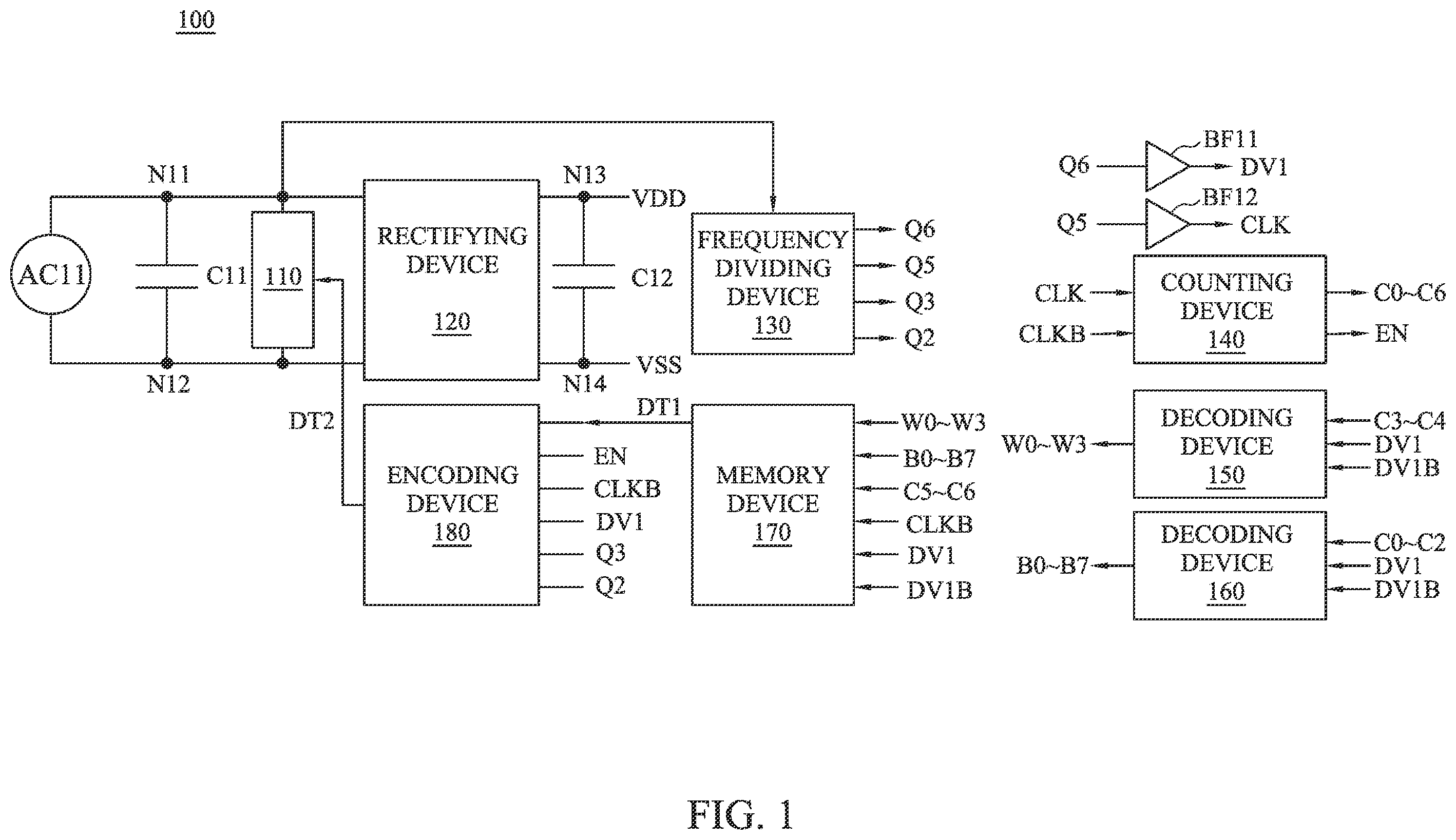
is a schematic diagram of a memory chip 100 illustrated according to one embodiment of this disclosure. In some embodiments, the memory chip 100 may implemented by a communication chip of near field communication. As illustratively shown in , the memory chip 100 includes a communication device 110 , a rectifying device 120 , a frequency dividing device 130 , a counting device 140 , decoding devices 150 , 160 , a memory device 170 , an encoding device 180 and buffering devices BF 11 , BF 12 .
As illustratively shown in , the communication device 110 is configured to receive a voltage signal AC 11 at nodes N 11 and N 12 . The rectifying device 120 is configured to receive the voltage signal AC 11 at the nodes N 11 and N 12 , and configured to generate voltage signals VDD and VSS at nodes N 13 and N 14 , respectively, according to the voltage signal AC 11 . In some embodiments, the rectifying device 120 is configured to transform the voltage signal AC 11 into voltage signals VDD and VSS. In some embodiments, a voltage level of the voltage signal VDD is higher than a voltage level of the voltage signal VSS.
In some embodiments, the memory chip 100 further includes capacitors C 11 and C 12 . As illustratively shown in , the capacitor C 11 is configured to receive the voltage signal AC 11 at the nodes N 11 and N 12 . The capacitor C 12 is configured to receive the voltage signal VDD at the node N 13 , and configured to receive the voltage signal VSS at the node N 14 . In some embodiments, a capacitance of the capacitor C 11 is approximately thirty-nine pico-farad.
As illustratively shown in , the frequency dividing device 130 is configured to receive the voltage signal AC 11 at the node N 11 , and configured to generate voltage signals Q 2 , Q 3 , Q 5 and Q 6 according to the voltage signal AC 11 . In some embodiments, the voltage signals Q 2 , Q 3 , Q 5 and Q 6 are implemented as clock signals. In some embodiments, a frequency of the voltage signal Q 6 corresponds to a frequency of the voltage signal AC 11 , a frequency of the voltage signal Q 5 is approximately a half of the frequency of the voltage signal Q 6 , a frequency of the voltage signal Q 3 is approximately one-fourth of the frequency of the voltage signal Q 5 , a frequency of the voltage signal Q 2 is approximately a half of the frequency of the voltage signal Q 3 .
In some embodiments, the buffering device BF 11 is configured to generate a clock signal DV 1 according to the voltage signal Q 6 , and the buffering device BF 12 is configured to generate a clock signal CLK according to the voltage signal Q 5 . As illustratively shown in , an input terminal of the buffering device BF 11 is configured to receive the voltage signal Q 6 , an output terminal of the buffering device BF 11 is configured to output the clock signal CLK. In some embodiments, each of the buffering devices BF 11 and BF 12 includes one or more inverters coupled in series. In some embodiments, a frequency of the clock signal DV 1 is substantially equal to the frequency of the voltage signal Q 6 , and a frequency of the clock signal CLK is substantially equal to the frequency of the voltage signal Q 5 . Further details of the clock signals CLK and DV 1 are described below in embodiments associated with to .
As illustratively shown in , the counting device 140 is configured to generate clock signals C 0 -C 6 and an enable signal EN according to clock signals CLK and CLKB. In some embodiments, the clock signal CLKB is a complementary signal of the clock signal CLK. In some embodiments, a frequency of a signal is equal to a frequency of a complementary signal of the signal. In some embodiments, the counting device 140 is implemented by a non-synchronize counter. Further details of the clock signals C 0 -C 6 , CLKB and the enable signal EN are described below in embodiments associated with to .
As illustratively shown in , the decoding device 150 is configured to generate word line signals W 0 -W 3 according to the clock signals C 3 , C 4 , DV 1 and DV 1 B. The decoding device 160 is configured to generate bit line signals B 0 -B 7 according to the clock signals C 0 -C 2 , DV 1 and DV 1 B. In some embodiments, the clock signal DV 1 B is a complementary signal of the clock signal DV 1 . In some embodiments, the decoding devices 150 and 160 are implemented by synchronize decoders. Further details of the word line signals W 0 -W 3 , the bit line signals B 0 -B 7 and the clock signal DV 1 B are described below in embodiments associated with to .
As illustratively shown in , the memory device 170 is configured to generate a data signal DT 1 according to the word line signals W 0 -W 3 , the bit line signals B 0 -B 7 and the clock signals DV 1 , DV 1 B, C 5 , C 6 , CLKB.
As illustratively shown in , the encoding device 180 is configured to output a data signal DT 2 according to the data signal DT 1 , the enable signal EN and the clock signal DV 1 and the voltage signal Q 2 , Q 3 . In some embodiments, the encoding device 180 is configured to encode the data signal DT 1 according to ISO format, to generate the data signal DT 2 . In some embodiments, the encoding device 180 is configured to transmit the data signal DT 2 to the communication device 110 , and the communication device 110 is configured to transmit the data signal DT 2 to external apparatuses and/or devices.
is a schematic diagram of a memory chip 200 illustrated according to one embodiment of this disclosure. As illustratively shown in , the memory chip 200 includes a counting device 240 , decoding devices 250 , 260 and a memory device 270 . Referring to and , the memory chip 200 is an embodiment of the memory chip 100 . The counting device 240 , the decoding devices 250 , 260 and the memory device 270 correspond to the counting device 140 , the decoding devices 150 , 160 and the memory device 170 , respectively. Therefore, some descriptions are not repeated for brevity. In some embodiments, the memory device further includes various devices correspond to the communication device 110 , the rectifying device 120 , the frequency dividing device 130 , the encoding device 180 and the buffering devices BF 11 , BF 12 .
In some embodiments, the counting device 240 is configured to provide various signals, such as the clock signals C 3 -C 4 shown in , to the decoding device 250 , and configured to provide various signals, such as the clock signals C 0 -C 2 shown in , to the decoding device 260 . The decoding device 250 is configured to generate the word line signals W 0 -W 3 . The decoding device 260 is configured to generate the bit line signals B 0 -B 7 . The memory device 270 is configured to operate according to the word line signals W 0 -W 3 and the bit line signals B 0 -B 7 .
In some embodiments, the memory device 270 includes memory circuits 271 - 274 . In some embodiments, each of the memory circuits 271 - 274 is configured to operate synchronously according to the word line signals W 0 -W 3 and the bit line signals B 0 -B 7 . In some embodiments, each of the memory circuits 271 - 274 is configured to store thirty-two bits of data, in which the number of the thirty-two bits corresponds to the number of the word line signals W 0 -W 3 multiplying the number of the bit line signals B 0 -B 7 . In the embodiments described above, the memory device 270 is configured to store one hundred and twenty-eight bits of data. In some embodiments, each of the memory circuits 271 - 274 is implemented by a dynamic programmable read only memory. In some embodiments, each of the memory circuits 271 - 274 is referred to as a data bank.
In various embodiments, the memory device 270 may include various numbers of memory circuit, and the decoding device 250 is configured to generate word line signals with corresponding numbers.
In some approaches, a memory device only includes one memory circuit. An encoding device need to generate a large amount of word line signals to perform non-synchronize controlling to the memory circuit. As a result, the decoding device and a counting device configured to control the decoding device occupy a larger area, and may generate a short-circuit current when phases of the word line signal are overlapped.
Compared to the above approaches, in some embodiments of the present disclosure, the decoding device 250 performs synchronize controlling to the memory circuits 271 - 274 by the same word line signals W 0 -W 3 , such that the decoding device 250 and the counting device 240 occupy a smaller area, and short-circuit currents are reduced.
is a schematic diagram of a memory device 300 illustrated according to one embodiment of this disclosure. As illustratively shown in , the memory device 300 includes a memory circuit 310 and a controlling circuit 320 . Referring to and , the memory device 300 is an embodiment of the memory device 270 . Each of the memory circuits 271 - 274 may be implemented as the memory circuit 310 . Therefore, some descriptions are not repeated for brevity.
As illustratively shown in , the memory circuit 310 and the controlling circuit 320 are coupled to each other a node N 32 . In some embodiments, the controlling circuit 320 is configured to adjust a voltage level of the node N 32 according to an enable signal ENB and the pulse signal PL, to control the memory circuit 310 . The memory circuit 310 is configured to be activated or deactivated according to the voltage level of the node N 32 , and is configured to generate a data signal DT 31 according to a word line signal WM and a bit line signal BN when being activated. It is noted that N and M of the word line signal WM and the bit line signal BN are integers larger than or equal to zero. Referring to and , the data signal DT 31 is an embodiment of the data signal DT 1 , the word line signal WM corresponds to the word line signals W 0 -W 3 , and the bit line signal BN corresponds to the bit line signals B 0 -B 7 . In some embodiments, the enable signal ENB is a complementary signal of the enable signal EN.
In some embodiments, the memory circuit 310 includes switches T 31 and T 32 . As illustratively shown in , a control terminal of the switch T 31 is configured to receive the bit line signal BN, a terminal of the switch T 31 is coupled to the node N 32 , another terminal of the switch T 31 is coupled to a node N 31 . A control terminal of the switch T 32 is configured to receive the word line signal WM, a terminal of the switch T 32 is coupled to the node N 31 , another terminal of the switch T 32 is configured to receive the voltage signal VSS or a ground voltage signal.
In some embodiments, the controlling circuit 320 includes switches T 33 -T 35 . As illustratively shown in , a control terminal of the switch T 33 is configured to receive the enable signal ENB, a terminal of the switch T 33 is coupled to a node N 33 , another terminal of the switch T 33 is configured to receive the voltage signal VDD or other voltage signals having an enable voltage level. A control terminal of the switch T 34 is configured to receive the pulse signal PL, a terminal of the switch T 34 is coupled to the node N 33 , another terminal of the switch T 34 is coupled to the node N 32 . A control terminal of the switch T 35 is configured to receive the enable signal ENB, a terminal of the switch T 35 is coupled to the node N 32 , another terminal of the switch T 35 is configured to receive the voltage signal VSS or the ground voltage signal.
In some embodiments, a type of the switches T 31 , T 32 and T 35 is different from a type of the switches T 33 and T 34 . For example, the switches T 31 , T 32 and T 35 are implemented by N-type thin film transistors (NTFT), and the switches T 33 and T 34 are implemented by P-type thin film transistors (PTFT).
In some embodiments, when the switch T 33 is turned on according to the enable signal ENB, the switch T 35 is turned off according to the enable signal ENB. When the switch T 33 is turned off according to the enable signal ENB, the switch T 35 is turned on according to the enable signal ENB.
In some embodiments, the switch T 35 is configured to be turned on to pull the voltage level of the node N 32 to a voltage level of the voltage signal VSS. When the node N 32 has the voltage level of the voltage signal VSS, a voltage difference between the nodes N 32 and N 34 is substantially equal to zero, and the memory circuit 310 does not generate the data signal DT 31 . Alternatively stated, the switch T 35 is configured to be turned on to deactivate the memory circuit 310 .
In some embodiments, the switch T 33 is configured to be turned on to pull the voltage level of the node N 33 to a voltage level of the voltage signal VDD. When the node N 33 have the voltage level of the voltage signal VDD, the switch T 34 may be turned to charge the node N 32 , such that the memory circuit 310 may generate the data signal DT 31 according to the word line signal WM and the bit line signal BN. Alternatively stated, the switch T 33 is configured to be turned on to activate the memory circuit 310 .
In some approaches, a node for outputting data signals in a memory device needs to be charged frequently, and a control circuit needs to provide a larger current, such that the required area is larger and leakage currents tend to be generated.
Compared to the above approaches, in some embodiments of the present disclosure, the controlling circuit 320 is configured to deactivate or activate the memory circuit 310 according to the enable signal ENB. The memory circuit 310 does not have a current passing through when being deactivated, and the memory circuit 310 has a smaller current passing through when being activated. The controlling circuit 320 is configured to charge the node N 32 at proper moments according to the pulse signal PL. As a result, the required area of the memory device 300 is smaller and leakage currents are reduced. Accordingly, a signal quality of the data signal DT 31 is better.
is a schematic diagram of a memory device 400 illustrated according to one embodiment of this disclosure. Referring to and , the memory device 400 is an embodiment of the memory device 170 . As illustratively shown in , the memory device 400 includes memory circuits 410 - 413 and controlling circuits 420 - 423 . Referring to and , the memory device 400 is an embodiment of the memory device 270 . The memory circuits 410 - 413 correspond to the memory circuits 271 - 274 , respectively. Therefore, some descriptions are not repeated for brevity.
As illustratively shown in , the memory circuit 410 is coupled to the controlling circuit 420 at a node N 40 , the memory circuit 411 is coupled to the controlling circuit 421 at a node N 41 , the memory circuit 412 is coupled to the controlling circuit 422 at a node N 42 , the memory circuit 413 is coupled to the controlling circuit 423 at a node N 43 . In some embodiments, the nodes N 40 -N 43 are electrically isolated from each other.
In some embodiments, the controlling circuit 420 is configured to control the memory circuit 410 according to an enable signal ENB 0 and the pulse signal PL, such that the memory circuit 410 generates a data signal DT 40 at the node N 40 . In some embodiments, the controlling circuit 420 includes switches T 403 -T 405 . Referring to and , configurations of the switches T 403 -T 405 are similar with the configurations of the switches T 33 -T 35 , and operations of the controlling circuit 420 controlling the memory circuit 410 generating the data signal DT 40 according to the enable signal ENB 0 and the pulse signal PL are similar with the operations of the controlling circuit 320 controlling the memory circuit 310 generating the data signal DT 31 according to the enable signal ENB and the pulse signal PL. Therefore, some descriptions are not repeated for brevity.
In some embodiments, the controlling circuit 421 is configured to control the memory circuit 411 according to an enable signal ENB 1 and the pulse signal PL, such that the memory circuit 411 generates a data signal DT 41 at the node N 41 . In some embodiments, the controlling circuit 421 includes switches T 413 -T 415 . Referring to and , configurations of the switches T 413 -T 415 are similar with the configurations of the switches T 33 -T 35 , and operations of the controlling circuit 421 controlling the memory circuit 411 generating the data signal DT 41 according to the enable signal ENB 1 and the pulse signal PL are similar with the operations of the controlling circuit 320 controlling the memory circuit 310 generating the data signal DT 31 according to the enable signal ENB and the pulse signal PL. Therefore, some descriptions are not repeated for brevity.
In some embodiments, the controlling circuit 422 is configured to control the memory circuit 412 according to an enable signal ENB 2 and the pulse signal PL, such that the memory circuit 412 generates a data signal DT 42 at the node N 42 . In some embodiments, the controlling circuit 422 includes switches T 423 -T 425 . Referring to and , configurations of the switches T 423 -T 425 are similar with the configurations of the switches T 33 -T 35 , and operations of the controlling circuit 422 controlling the memory circuit 412 generating the data signal DT 42 according to the enable signal ENB 2 and the pulse signal PL are similar with the operations of the controlling circuit 320 controlling the memory circuit 310 generating the data signal DT 31 according to the enable signal ENB and the pulse signal PL. Therefore, some descriptions are not repeated for brevity.
In some embodiments, the controlling circuit 423 is configured to control the memory circuit 413 according to an enable signal ENB 3 and the pulse signal PL, such that the memory circuit 413 generates a data signal DT 43 at the node N 43 . In some embodiments, the controlling circuit 423 includes switches T 433 -T 435 . Referring to and , configurations of the switches T 433 -T 435 are similar with the configurations of the switches T 33 -T 35 , and operations of the controlling circuit 423 controlling the memory circuit 413 generating the data signal DT 43 according to the enable signal ENB 3 and the pulse signal PL are similar with the operations of the controlling circuit 320 controlling the memory circuit 310 generating the data signal DT 31 according to the enable signal ENB and the pulse signal PL. Therefore, some descriptions are not repeated for brevity.
Referring to and , in some embodiments, each of the memory circuits 410 - 413 is configured to generate a corresponding one of the data signals DT 40 -DT 43 according to the word line signals W 0 -W 4 . In some embodiments, each of the memory circuits 410 - 413 is configured to generate the corresponding one of the data signals DT 40 -DT 43 according to the bit line signals B 0 -B 7 .
In some embodiments, a type of the switches T 403 , T 404 , T 413 , T 414 , T 423 , T 424 , T 433 and T 434 is different from a type of the switches T 405 , T 415 , T 425 and T 435 . For example, the switches T 403 , T 404 , T 413 , T 414 , T 423 , T 424 , T 433 and T 434 are implemented by PTFT, and the switches T 405 , T 415 , T 425 and T 435 are implemented by NTFT.
is a timing diagram 500 of the memory device 400 shown in performing operations according to the enable signals ENB 0 -ENB 3 , illustrated according to one embodiment of this disclosure. As illustratively shown in , the timing diagram 500 includes periods P 51 -P 510 arranged continuously in order.
As illustratively shown in , during the period P 53 , the enable signal ENB 0 has a voltage level VL, and the enable signals ENB 1 -ENB 3 have a voltage level VH. Referring to and , during the period P 53 , in response to the enable signal ENB 0 having the voltage level VL, the switch T 403 is turned on and the switch T 405 is turned off, such that the memory circuit 410 generates the data signal DT 40 . During the period P 53 , in response to the enable signals ENB 1 -ENB 3 having the voltage level VH, the switches T 415 , T 425 and T 435 are turned on and the switches T 413 , T 423 and T 433 are turned off, such that the memory circuits 411 - 413 are deactivated. In some embodiments, each of the memory circuits 410 - 413 does not generate a corresponding one of the data signals DT 40 -DT 43 when being deactivated.
As illustratively shown in , during the period P 54 , the enable signal ENB 1 has the voltage level VL, and the enable signals ENB 0 , ENB 2 and ENB 3 have the voltage level VH. Referring to and , during the period P 54 , in response to the enable signal ENB 1 having the voltage level VL, the switch T 413 is turned on and the switch T 415 is turned off, such that the memory circuit 411 generates the data signal DT 41 . During the period P 54 , in response to the enable signals ENB 0 , ENB 2 and ENB 3 having the voltage level VH, the switches T 405 , T 425 and T 435 are turned on and the switches T 403 , T 423 and T 433 are turned off, such that the memory circuits 410 , 412 and 413 are deactivated.
As illustratively shown in , during the period P 55 , the enable signal ENB 2 has the voltage level VL, and the enable signals ENB 0 , ENB 1 and ENB 3 have the voltage level VH. Referring to and , during the period P 55 , in response to the enable signal ENB 2 having the voltage level VL, the switch T 423 is turned on and the switch T 425 is turned off, such that the memory circuit 412 generates the data signal DT 42 . During the period P 55 , in response to the enable signals ENB 0 , ENB 1 and ENB 3 having the voltage level VH, the switches T 405 , T 415 and T 435 are turned on and the switches T 403 , T 413 and T 433 are turned off, such that the memory circuits 410 , 411 and 413 are deactivated.
As illustratively shown in , during the period P 56 , the enable signal ENB 3 has the voltage level VL, and the enable signals ENB 0 -ENB 2 have the voltage level VH. Referring to and , during the period P 56 , in response to the enable signal ENB 3 having the voltage level VL, the switch T 433 is turned on and the switch T 435 is turned off, such that the memory circuit 413 generates the data signal DT 43 . During the period P 56 , in response to the enable signals ENB 0 -ENB 2 having the voltage level VH, the switches T 415 , T 425 and T 405 are turned on and the switches T 413 , T 423 and T 403 are turned off, such that the memory circuits 410 - 412 are deactivated.
Referring to to , in some embodiments, during the periods P 53 -P 56 , the memory circuits 410 - 413 are activated in order, and generates the data signals DT 40 -DT 43 in order according to the same word line signals W 0 -W 3 and the same bit line signals B 0 -B 7 when being activated.
As illustratively shown in , operations of the periods P 57 -P 510 are similar with the operations of the periods P 53 -P 56 , respectively, and operations of the periods P 51 -P 52 are similar with the operations of the periods P 55 -P 56 , respectively. Therefore, some descriptions are not repeated for brevity.
A is a schematic diagram of a logic circuit 600 A illustrated according to one embodiment of this disclosure. Referring to and A, in some embodiments, the logic circuit 600 A is included in the memory device 400 . Referring to , and A , in some embodiments, the logic circuit 600 A is configured to generate the enable signals ENB 0 -ENB 3 according to the clock signals C 5 and C 6 .
In some embodiments, the logic circuit 600 A includes logic elements NR 60 -NR 63 and IV 60 -IV 63 . In some embodiments, each of the logic elements NR 60 -NR 63 is implemented by a NOR logic gate, and each of the logic elements IV 60 -IV 63 is implemented by an inverter. In some embodiments, the logic elements IV 60 -IV 63 are configured to operate according to the clock signal DV 1 . In various embodiments, the logic elements NR 60 -NR 63 and IV 60 -IV 63 may be implemented by various types of logic elements.
As illustratively shown in A , two input terminals of the logic element NR 60 are configured to receive the clock signals C 5 and C 6 , respectively, and an output terminal of the logic element NR 60 is configured to output an enable signal EN 0 . An input terminal of the logic element IV 60 is configured to receive the enable signal EN 0 , and an output terminal of the logic element IV 60 is configured to output the enable signal ENB 0 . In some embodiments, the enable signal EN 0 is a complementary signal of the enable signal ENB 0 .
As illustratively shown in A , two input terminals of the logic element NR 61 are configured to receive clock signals CB 5 and C 6 , respectively, and an output terminal of the logic element NR 61 is configured to output an enable signal EN 1 . An input terminal of the logic element IV 61 is configured to receive the enable signal EN 1 , and an output terminal of the logic element IV 61 is configured to output the enable signal ENB 1 . In some embodiments, the enable signal EN 1 is a complementary signal of the enable signal ENB 1 , and the clock signal CB 5 is a complementary signal of the clock signal C 5 .
As illustratively shown in A , two input terminals of the logic element NR 62 are configured to receive clock signals C 5 and CB 6 , respectively, and an output terminal of the logic element NR 62 is configured to output an enable signal EN 2 . An input terminal of the logic element IV 62 is configured to receive the enable signal EN 2 , and an output terminal of the logic element IV 62 is configured to output the enable signal ENB 2 . In some embodiments, the enable signal EN 2 is a complementary signal of the enable signal ENB 2 , and the clock signal CB 6 is a complementary signal of the clock signal C 6 .
As illustratively shown in A , two input terminals of the logic element NR 63 are configured to receive the clock signals CB 5 and CB 6 , respectively, and an output terminal of the logic element NR 63 is configured to output an enable signal EN 3 . An input terminal of the logic element IV 63 is configured to receive the enable signal EN 3 , and an output terminal of the logic element IV 63 is configured to output the enable signal ENB 3 . In some embodiments, the enable signal EN 3 is a complementary signal of the enable signal ENB 3 .
B is a schematic diagram of a logic circuit 600 B illustrated according to one embodiment of this disclosure. Referring to and B , in some embodiments, the logic circuit 600 B is included in the memory device 400 . Referring to , and B , the logic circuit 600 B is configured to generate the data signal DT 1 according to the data signal DT 40 -DT 43 .
In some embodiments, the logic circuit 600 A includes a logic element OR 61 . In some embodiments, the logic element OR 61 is implemented by an OR logic gate. In various embodiments, the logic element OR 61 may implemented by various types of logic elements.
As illustratively shown in B , the logic element OR 61 is configured to receive the data signal DT 40 -DT 43 , and configured to perform an OR operation to the data signal DT 40 -DT 43 to generate the data signal DT 1 . In some embodiments, the data signal DT 1 includes information of the data signal DT 40 -DT 43 . For example, each of the data signal DT 40 -DT 43 includes thirty-two bits of information, and the data signal DT 1 includes corresponding one hundred and twenty-eight bits of information.
is a schematic diagram of a memory device 700 illustrated according to one embodiment of this disclosure. As illustratively shown in , the memory device 700 includes a memory circuit 710 and a controlling circuit 720 . The controlling circuit 720 is configured to control the memory circuit 710 , such that the memory circuit 710 generates a data signal DT 71 at a node N 71 . Referring to and , the memory device 700 is an embodiment of the memory device 300 . Operations of the memory circuit 710 and the controlling circuit 720 generating the data signal DT 71 correspond to the operations of the memory circuit 310 and the controlling circuit 320 generating the data signal DT 31 . Therefore, some descriptions are not repeated for brevity.
In some embodiments, the controlling circuit 720 includes switches T 73 -T 75 . In some embodiments, the switch T 75 is implemented by a NTFT, and the switches T 73 and T 74 are implemented by a PTFT. The switches T 73 -T 75 are configured to operate according to the enable signal ENB and the pulse signal PL. Referring to and , configurations of the switches T 73 -T 75 and operations of the switches T 73 -T 75 according to the enable signal ENB and the pulse signal PL are similar with the configurations of the switches T 33 -T 35 and operations of the switches T 33 -T 35 according to the enable signal ENB and the pulse signal PL. Therefore, some descriptions are not repeated for brevity.
In some embodiments, the memory circuit 710 includes switches Z 0 -Z 7 , X 00 -X 03 , X 10 -X 13 , X 20 -X 23 , X 30 -X 33 , X 40 -X 43 , X 50 -X 53 , X 60 -X 63 and X 70 -X 73 . Referring to and , the memory circuit 710 is an embodiment of each of the memory circuits 410 - 413 . In some embodiments, each of the memory circuits 410 - 413 has the configuration of the memory circuit 710 . In the embodiments described above, operations of the memory circuits 410 - 413 generating the data signals DT 40 -DT 43 are similar with operations of the memory circuit 710 generating the data signal DT 71 . In some embodiments, the switches Z 0 -Z 7 , X 00 -X 03 , X 10 -X 13 , X 20 -X 23 , X 30 -X 33 , X 40 -X 43 , X 50 -X 53 , X 60 -X 63 and X 70 -X 73 are implemented as NTFT.
As illustratively shown in , control terminals of the switches Z 0 -Z 7 are configured to receive the bit line signals B 0 -B 7 , respectively. First terminals the switches Z 0 -Z 7 are coupled to a node N 71 . Second terminals the switches Z 0 -Z 7 are coupled to nodes N 72 -N 79 , respectively.
As illustratively shown in , control terminals of the switches X 00 , X 10 , X 20 , X 30 , X 40 , X 50 , X 60 and X 70 are configured to receive the word line signal W 0 , control terminals of the switches X 01 , X 11 , X 21 , X 31 , X 41 , X 51 , X 61 and X 71 are configured to receive the word line signal W 1 , control terminals of the switches X 02 , X 12 , X 22 , X 32 , X 42 , X 52 , X 62 and X 72 are configured to receive the word line signal W 2 , control terminals of the switches X 03 , X 13 , X 23 , X 33 , X 43 , X 53 , X 63 and X 73 are configured to receive the word line signal W 3 .
As illustratively shown in , first terminals of the switches X 00 -X 03 are coupled to the node N 79 , first terminals of the switches X 10 -X 13 are coupled to the node N 78 , first terminals of the switches X 20 -X 23 are coupled to the node N 77 , first terminals of the switches X 30 -X 33 are coupled to the node N 76 , first terminals of the switches X 40 -X 43 are coupled to the node N 75 , first terminals of the switches X 50 -X 53 are coupled to the node N 74 , first terminals of the switches X 60 -X 63 are coupled to the node N 73 , first terminals of the switches X 70 -X 73 are coupled to the node N 72 . Second terminals of the switches Z 0 -Z 7 , X 00 -X 03 , X 10 -X 13 , X 20 -X 23 , X 30 -X 33 , X 40 -X 43 , X 50 -X 53 , X 60 -X 63 and X 70 -X 73 are configured to receive the voltage signal VSS or the ground voltage.
In the embodiment shown in , the memory circuit 710 is configured to store thirty-two bits of data. Each of the switches X 00 -X 03 , X 10 -X 13 , X 20 -X 23 , X 30 -X 33 , X 40 -X 43 , X 50 -X 53 , X 60 -X 63 and X 70 -X 73 is configured to read one corresponding bit of data, to generate the data signal DT 71 having thirty-two bits.
Referring to and , for integers i and j larger than or equal to zero and smaller than or equal to seven, and a integer k larger than or equal to zero and smaller than or equal to three, configurations of the switches Zi and Xjk and operations of the switches Zi and Xjk generating the data signal DT 71 according to the word line signals W 0 -W 3 and the bit line signals B 0 -B 7 are similar with the configurations of the switches T 31 and T 32 and operations of the switches T 31 and T 32 generating the data signal DT 31 according to the word line signal WM and the bit line signal BN. Therefore, some descriptions are not repeated for brevity.
In some embodiments, the memory circuit 710 further includes a cutting area 712 . As illustratively shown in , the cutting area 712 is located between the switches Z 0 -Z 7 , X 00 -X 03 , X 10 -X 13 , X 20 -X 23 , X 30 -X 33 , X 40 -X 43 , X 50 -X 53 , X 60 -X 6 , X 70 -X 73 and a voltage source providing the voltage signal VSS. In some embodiments, the cutting area 712 includes bus lines configured to perform laser cutting.
is a schematic diagram of a logic circuit 800 illustrated according to one embodiment of this disclosure. Referring to and , in some embodiments, the logic circuit 800 is included in the decoding device 160 . As illustratively shown in , the logic circuit 800 is configured to generate the bit line signals B 0 -B 7 according to clock signals C 0 -C 2 and CB 0 -CB 2 . In some embodiments, the clock signals CB 0 -CB 2 are complementary signals of the clock signals C 0 -C 2 , respectively.
In some embodiments, the logic circuit 800 includes logic elements ND 81 -ND 84 , NR 81 -NR 88 , NV 81 -NV 86 and IV 81 -IV 86 . In some embodiments, each of the logic elements ND 81 -ND 84 is implemented by a NAND logic gate, each of the logic elements NR 81 -NR 88 is implemented by a NOR logic gate, and each of the logic elements NV 81 -NV 86 and IV 81 -IV 86 is implemented by an inverter. In some embodiments, each of the logic elements IV 81 -IV 86 is configured to operate according to the clock signal DV 1 .
As illustratively shown in , an input terminal of the logic element IV 81 is configured to receive the clock signal CB 2 , and an output terminal of the logic element IV 81 is coupled to an input terminal of the logic element NV 81 . An output terminal of the logic element NV 81 is configured to output the enable signal EL 2 . An input terminal of the logic element IV 82 is configured to receive the clock signal C 2 , and an output terminal of the logic element IV 82 is coupled to an input terminal of the logic element NV 82 . An output terminal of the logic element NV 82 is configured to output the enable signal ELB 2 .
As illustratively shown in , two input terminals of the logic element ND 81 is configured to receive the clock signal C 1 and C 0 , respectively, and an output terminal of the logic element ND 81 is coupled to an input terminal of the logic element IV 83 . An output terminal of the logic element IV 83 is coupled to an input terminal of the logic element NV 83 . An input terminal of the logic element NR 81 is configured to receive the enable signal EL 2 , another input terminal of the logic element NR 81 is coupled to an output terminal of the logic element NV 83 , and an output terminal of the logic element NR 81 is configured to output the bit line signal B 0 . An input terminal of the logic element NR 82 is configured to receive the enable signal ELB 2 , another input terminal of the logic element NR 82 is coupled to the output terminal of the logic element NV 83 , and an output terminal of the logic element NR 82 is configured to output the bit line signal B 4 .
As illustratively shown in , two input terminals of the logic element ND 82 is configured to receive the clock signal C 1 and CB 0 , respectively, and an output terminal of the logic element ND 82 is coupled to an input terminal of the logic element IV 84 . An output terminal of the logic element IV 84 is coupled to an input terminal of the logic element NV 84 . An input terminal of the logic element NR 83 is configured to receive the enable signal EL 2 , another input terminal of the logic element NR 83 is coupled to an output terminal of the logic element NV 84 , and an output terminal of the logic element NR 83 is configured to output the bit line signal B 1 . An input terminal of the logic element NR 84 is configured to receive the enable signal ELB 2 , another input terminal of the logic element NR 84 is coupled to the output terminal of the logic element NV 84 , and an output terminal of the logic element NR 84 is configured to output the bit line signal B 5 .
As illustratively shown in , two input terminals of the logic element ND 83 is configured to receive the clock signal CB 1 and C 0 , respectively, and an output terminal of the logic element ND 83 is coupled to an input terminal of the logic element IV 85 . An output terminal of the logic element IV 85 is coupled to an input terminal of the logic element NV 85 . An input terminal of the logic element NR 85 is configured to receive the enable signal EL 2 , another input terminal of the logic element NR 85 is coupled to an output terminal of the logic element NV 85 , and an output terminal of the logic element NR 85 is configured to output the bit line signal B 2 . An input terminal of the logic element NR 86 is configured to receive the enable signal ELB 2 , another input terminal of the logic element NR 86 is coupled to the output terminal of the logic element NV 85 , and an output terminal of the logic element NR 86 is configured to output the bit line signal B 6 .
As illustratively shown in , two input terminals of the logic element ND 84 is configured to receive the clock signal CB 1 and CB 0 , respectively, and an output terminal of the logic element ND 84 is coupled to an input terminal of the logic element IV 86 . An output terminal of the logic element IV 86 is coupled to an input terminal of the logic element NV 86 . An input terminal of the logic element NR 87 is configured to receive the enable signal EL 2 , another input terminal of the logic element NR 87 is coupled to an output terminal of the logic element NV 86 , and an output terminal of the logic element NR 87 is configured to output the bit line signal B 3 . An input terminal of the logic element NR 88 is configured to receive the enable signal ELB 2 , another input terminal of the logic element NR 88 is coupled to the output terminal of the logic element NV 86 , and an output terminal of the logic element NR 88 is configured to output the bit line signal B 7 .
is a schematic diagram of a logic circuit 900 illustrated according to one embodiment of this disclosure. Referring to and , in some embodiments, the logic circuit 900 is included in the decoding device 150 . As illustratively shown in , the logic circuit 900 is configured to generate the pulse signal PL according to clock signals CLKB and DV 1 B, and configured to generate word line signals W 0 -W 3 according to the pulse signal PL, the clock signals C 3 -C 4 and CB 3 -CB 4 . In some embodiments, the clock signals CB 3 -CB 4 are complementary signals of the clock signals C 3 -C 4 , respectively.
In some embodiments, the logic circuit 900 includes logic elements AD 91 -AD 94 , NR 91 -NR 95 , NV 91 -NV 94 and IV 91 -IV 94 . In some embodiments, each of the logic elements AD 91 -AD 94 is implemented by an AND logic gate, each of the logic elements NR 91 -NR 95 is implemented by a NOR logic gate, and each of the logic elements NV 91 -NV 94 and IV 91 -IV 94 is implemented by an inverter. In some embodiments, each of the logic elements IV 91 -IV 94 is configured to operate according to the clock signal DV 1 .
As illustratively shown in , two input terminals of the logic element NR 91 is configured to receive the clock signals CLKB and DV 1 B, respectively, and an output terminal of the logic element NR 91 is configured to output the pulse signal PL.
As illustratively shown in , two input terminals of the logic element NR 92 is configured to receive the clock signals C 3 and C 4 , respectively, and an output terminal of the logic element NR 92 is coupled to an input terminal of the logic element IV 91 . An output terminal of the logic element IV 91 is coupled to an input terminal of the logic element NV 91 . An input terminal of the logic element AD 91 is coupled to an output terminal of the logic element NV 91 , another input terminal of the logic element AD 91 is configured to receive the pulse signal PL, and an output terminal of the logic element AD 91 is configured to output the word line signal W 0 .
As illustratively shown in , two input terminals of the logic element NR 93 is configured to receive the clock signals CB 3 and C 4 , respectively, and an output terminal of the logic element NR 93 is coupled to an input terminal of the logic element IV 92 . An output terminal of the logic element IV 92 is coupled to an input terminal of the logic element NV 92 . An input terminal of the logic element AD 92 is coupled to an output terminal of the logic element NV 92 , another input terminal of the logic element AD 92 is configured to receive the pulse signal PL, and an output terminal of the logic element AD 92 is configured to output the word line signal W 1 .
As illustratively shown in , two input terminals of the logic element NR 94 is configured to receive the clock signals C 3 and CB 4 , respectively, and an output terminal of the logic element NR 94 is coupled to an input terminal of the logic element IV 93 . An output terminal of the logic element IV 93 is coupled to an input terminal of the logic element NV 93 . An input terminal of the logic element AD 93 is coupled to an output terminal of the logic element NV 93 , another input terminal of the logic element AD 93 is configured to receive the pulse signal PL, and an output terminal of the logic element AD 93 is configured to output the word line signal W 2 .
As illustratively shown in , two input terminals of the logic element NR 95 is configured to receive the clock signals CB 3 and CB 4 , respectively, and an output terminal of the logic element NR 95 is coupled to an input terminal of the logic element IV 94 . An output terminal of the logic element IV 94 is coupled to an input terminal of the logic element NV 94 . An input terminal of the logic element AD 94 is coupled to an output terminal of the logic element NV 94 , another input terminal of the logic element AD 94 is configured to receive the pulse signal PL, and an output terminal of the logic element AD 94 is configured to output the word line signal W 3 .
is a timing diagram 1000 of the memory chip 100 shown in generating the data signal DT 1 , illustrated according to one embodiment of this disclosure. As illustratively shown in , the timing diagram 1000 includes periods Q 1 -Q 15 arranged continuously in order. Referring to , and , in the embodiment shown in , the memory device 170 may be implemented by the memory device 400 and/or the memory device 700 , to operate according to the timing diagram 1000 .
Referring to and , the period P 53 corresponds to the periods Q 1 -Q 15 . In some embodiments, during the periods Q 1 -Q 15 , the enable signal ENB 0 has the voltage level VL, and the enable signals ENB 1 -ENB 3 has the voltage level VH. Accordingly, referring to , and , during the periods Q 1 -Q 15 , the memory circuit 410 is configured to generate the data signal DT 40 at the node N 40 , and the memory circuits 411 - 413 are deactivated.
As illustratively shown in , during the period Q 1 , the clock signals CLK, C 0 -C 2 and DV 1 have the voltage level VL, such that the pulse signal PL has the voltage level VH, the bit line signal B 7 and the word line signal W 0 have the voltage level VL.
Referring to and , during the period Q 1 , the switch Z 7 is turned off according to the bit line signal B 7 , the switch X 70 is turned off according to the word line signal W 0 , and the switch T 74 is turned off according to the pulse signal PL.
As illustratively shown in , during the period Q 2 , the clock signals CLK and C 0 -C 2 have the voltage level VL, and the clock signal DV 1 has the voltage level VH, such that the pulse signal PL has the voltage level VL, the bit line signal B 7 has the voltage level VH, and the word line signal W 0 has the voltage level VL.
Referring to and , during the period Q 2 , the switch Z 7 is turned on according to the bit line signal B 7 , the switch X 70 is turned off according to the word line signal W 0 , the switch T 74 is turned on according to the pulse signal PL, and the switch T 73 is turned on according to the enable signal ENB. At this moment, the switches T 73 and T 74 provide the voltage signal VDD to the node N 71 to charge the node N 71 , such that the data signal DT 71 is pulled to the voltage level VH. Accordingly, the data signal DT 1 including the data signal DT 71 has the voltage level VH. In some embodiments, the period Q 2 is referred to as a charging period.
As illustratively shown in , during the period Q 3 , the clock signals DV 1 and C 0 -C 2 have the voltage level VL, and the clock signal CLK has the voltage level VH, such that the pulse signal PL has the voltage level VH, the bit line signal B 7 has the voltage level VH, and the word line signal W 0 has the voltage level VH.
Referring to and , during the period Q 3 , the switch Z 7 is turned on according to the bit line signal B 7 , the switch X 70 is turned on according to the word line signal W 0 , the switch T 74 is turned off according to the pulse signal PL, and the switch T 73 is turned on according to the enable signal ENB. At this moment, the node N 71 is discharged through the switches Z 7 and X 70 to generate the data signal DT 71 .
In the embodiment shown in , a bit corresponding to the switches Z 7 and X 70 has a first logic value, such as a logic value of 1, such that the data signal DT 71 has the voltage level VH during the period Q 3 . Accordingly, the data signal DT 1 including information of the data signal DT 71 has the voltage level VH.
As illustratively shown in , during the period Q 4 , the clock signals C 0 -C 2 have the voltage level VL, and the clock signals CLK and DV 1 have the voltage level VH, such that the pulse signal PL has the voltage level VH, the bit line signal B 7 has the voltage level VH, and the word line signal W 0 has the voltage level VH.
Referring to and , during the period Q 4 , the switch Z 7 is turned on according to the bit line signal B 7 , the switch X 70 is turned on according to the word line signal W 0 , the switch T 74 is turned off according to the pulse signal PL, and the switch T 73 is turned on according to the enable signal ENB. At this moment, the node N 71 is discharged through the switches Z 7 and X 70 to generate the data signal DT 71 .
In the embodiment shown in , the bit corresponding to the switches Z 7 and X 70 has the first logic value, such that the data signal DT 71 has the voltage level VH during the period Q 4 . Accordingly, the data signal DT 1 including information of the data signal DT 71 has the voltage level VH.
As illustratively shown in , during the period Q 5 , the clock signals CLK, C 1 -C 2 and DV 1 have the voltage level VL, and the clock signal C 0 has the voltage level VH, such that the pulse signal PL has the voltage level VH, the bit line signal B 7 has the voltage level VH, and the word line signal W 0 has the voltage level VH.
Referring to and , during the period Q 5 , the switch Z 7 is turned on according to the bit line signal B 7 , the switch X 70 is turned on according to the word line signal W 0 , the switch T 74 is turned off according to the pulse signal PL, and the switch T 73 is turned on according to the enable signal ENB. At this moment, the node N 71 is discharged through the switches Z 7 and X 70 to generate the data signal DT 71 . In some embodiments, the periods Q 3 -Q 5 are referred to as discharging periods.
In the embodiment shown in , the bit corresponding to the switches Z 7 and X 70 has the first logic value, such that the data signal DT 71 has the voltage level VH during the period Q 5 . Accordingly, the data signal DT 1 including information of the data signal DT 71 has the voltage level VH.
As illustratively shown in , during the period Q 6 , the clock signals CLK and C 1 -C 2 have the voltage level VL, and the clock signals C 0 and DV 1 have the voltage level VH, such that the pulse signal PL, the bit line signal B 7 and the word line signal W 0 have the voltage level VL, and the bit line signal B 6 has the voltage level VH.
Referring to and , during the period Q 6 , the switch Z 7 is turned off according to the bit line signal B 7 , the switch Z 6 is turned on according to the bit line signal B 6 , the switch X 60 is turned off according to the word line signal W 0 , the switch T 74 is turned on according to the pulse signal PL, and the switch T 73 is turned on according to the enable signal ENB. At this moment, the switches T 73 and T 74 provide the voltage signal VDD to the node N 71 to charge the node N 71 , such that the data signal DT 71 is pulled to the voltage level VH. Accordingly, the data signal DT 1 including information of the data signal DT 71 has the voltage level VH. In some embodiments, the period Q 6 is referred to as a charging period.
As illustratively shown in , during the period Q 7 , the pulse signal PL has the voltage level VH, the bit line signal B 6 has the voltage level VH, and the word line signal W 0 has the voltage level VH, such that the switch Z 6 is turned on according to the bit line signal B 6 , the switch X 60 is turned on according to the word line signal W 0 , the switch T 74 is turned off according to the bit line signal B 6 , and the switch T 73 is turned on according to the enable signal ENB. At this moment, the node N 71 is discharged through the switches Z 6 and X 60 to generate the data signal DT 71 and the corresponding data signal DT 1 .
In some embodiments, operations of the memory device 700 discharging through the switches Z 6 and X 60 according to the pulse signal PL, the bit line signal B 6 and the word line signal W 0 during the period Q 7 , to generate the data signal DT 71 are similar with the operations of the memory device 700 discharging through the switches Z 7 and X 70 according to the pulse signal PL, the bit line signal B 7 and the word line signal W 0 during the periods Q 3 -Q 5 , to generate the data signal DT 71 . Therefore, some descriptions are not repeated for brevity.
As illustratively shown in , during the period Q 8 , the bit line signals B 6 and B 5 have the voltage level VL, and the bit line signal B 5 has the voltage level VH. In some embodiments, operations of the memory device 700 charging the node N 71 during the period Q 8 according to the pulse signal PL, the bit line signal B 5 and the word line signal W 0 , and discharge through the switches Z 5 and X 50 to generate the data signal DT 71 are similar with the operations of the memory device 700 charging the node N 71 during the periods Q 2 -Q 5 according to the pulse signal PL, the bit line signal B 7 and the word line signal W 0 , and discharge through the switches Z 7 and X 70 to generate the data signal DT 71 . Therefore, some descriptions are not repeated for brevity.
As illustratively shown in , the bit line signals B 4 -B 0 have the voltage level VH during the periods Q 9 -Q 13 , respectively. The node N 71 is discharged through the switches Z 4 -Z 0 during the periods Q 9 -Q 13 , respectively, to generate the data signal DT 71 . Each of operations of the memory device 700 during the period Q 9 corresponding to the bit line signal B 4 , operations of the memory device 700 during the period Q 10 corresponding to the bit line signal B 3 , operations of the memory device 700 during the period Q 11 corresponding to the bit line signal B 2 , operations of the memory device 700 during the period Q 12 corresponding to the bit line signal B 1 , and operations of the memory device 700 during the period Q 13 corresponding to the bit line signal B 0 is similar with the operations of the memory device 700 during the periods Q 2 -Q 5 corresponding to the bit line signal B 7 . Therefore, some descriptions are not repeated for brevity.
In the embodiment shown in , during the periods Q 11 -Q 13 , the bits correspond to the switches X 20 , X 10 and X 00 have a second logic value, such as a logic value of 0, such that the data signal DT 1 has the voltage level VL during the period Q 11 -Q 13 , when the word line signal W 0 has the voltage level VH.
Referring to and , during the periods Q 1 -Q 13 , the switches X 70 , X 60 , X 50 , X 40 , X 30 , X 20 , X 10 and X 00 configured to receive the word line signal W 0 generate the data signal DT 71 in order. In the embodiment shown in , the logic values of eight bits corresponding to the switches X 70 , X 60 , X 50 , X 40 , X 30 , X 20 , X 10 and X 00 are 1, 1, 1, 1, 1, 0, 0 and 0 in order.
As illustratively shown in , during the period Q 14 , the word line signal W 0 has the voltage level VL, and the word line signal W 1 (not shown in ) and the bit line signal B 7 have the voltage level VH. Referring to and , during the period Q 14 , the switch Z 7 is turned on according to the bit line signal B 7 , and the switch X 71 is turned on according to the word line signal W 1 . At this moment, the node N 71 is discharged through the switches Z 7 and X 71 to generate the data signal DT 71 .
As illustratively shown in , during the period Q 15 , the word line signal W 0 has the voltage level VL, and the word line signal W 1 (not shown in ) and the bit line signal B 6 have the voltage level VH. Referring to and , during the period Q 15 , the switch Z 6 is turned on according to the bit line signal B 6 , and the switch X 61 is turned on according to the word line signal W 1 . At this moment, the node N 71 is discharged through the switches Z 6 and X 61 to generate the data signal DT 71 .
In some embodiments, each of operations of the memory device 700 during the period Q 14 corresponding to the bit line signal B 7 and the word line signal W 1 , and operations of the memory device 700 during the period Q 15 corresponding to the bit line signal B 6 and the word line signal W 1 is similar with the operations of the memory device 700 during the periods Q 2 -Q 5 corresponding to the bit line signal B 7 and the word line signal W 1 . Therefore, some descriptions are not repeated for brevity.
In some embodiments, a time length of the periods Q 1 -Q 4 is approximately equal to 1/106000 second. In some embodiments, a frequency of the clock signal DV 1 is approximately equal to two hundred and twelve kHz.
is a timing diagram 1100 of the memory chip 100 shown in generating the data signal DT 1 , illustrated according to one embodiment of this disclosure. As illustratively shown in , the timing diagram 1100 includes periods J 1 -J 9 arranged continuously in order. Referring to , , B , in the embodiment shown in , the memory device 170 may be implemented by the memory device 400 and or the memory device 700 , and may include the logic circuit 600 B, to operate according to the timing diagram 1100 .
As illustratively shown in , during the period J 1 , the clock signals C 3 -C 6 have the voltage level VL, such that the word line signal W 0 and the enable signals ENB 1 -ENB 3 have the voltage level VH, and the word line signals W 1 -W 3 and the enable signal ENB 0 have the voltage level VL.
Referring to and , the switches X 00 , X 10 , X 20 , X 30 , X 40 , X 50 , X 60 and X 70 are turned on according to the word line signal W 0 , such that the memory device 700 generates the data signal DT 71 corresponding to the bits of the switches X 00 , X 10 , X 20 , X 30 , X 40 , X 50 , X 60 and X 70 .
Similarly, referring to and , during the period J 1 , the controlling circuit 420 is configured to activate the memory circuit 410 according to the enable signal ENB 0 , such that the memory circuit 410 generates the data signal DT 40 corresponding to the word line signal W 0 . At this moment, the controlling circuits 421 - 423 are configured to deactivate the memory circuits 411 - 413 , such that the nodes N 41 -N 43 have the voltage level VL.
As illustratively shown in , during the period J 2 , the clock signals C 4 -C 6 have the voltage level VL, the clock signal C 3 has the voltage level VH, such that the word line signal W 1 and the enable signals ENB 1 -ENB 3 have the voltage level VH, and the word line signals W 0 , W 2 -W 3 and the enable signal ENB 0 have the voltage level VL.
Referring to and , during the period J 2 , the switches X 01 , X 11 , X 21 , X 31 , X 41 , X 51 , X 61 and X 71 are turned on according to the word line signal W 1 , such that the memory device 700 generates the data signal DT 71 corresponding to the bits of the switches X 01 , X 11 , X 21 , X 31 , X 41 , X 51 , X 61 and X 71 .
Similarly, referring to and , during the period J 2 , the controlling circuit 420 is configured to activate the memory circuit 410 according to the enable signal ENB 0 , such that the memory circuit 410 generates the data signal DT 40 corresponding to the word line signal W 1 . At this moment, the controlling circuits 421 - 423 are configured to deactivate the memory circuits 411 - 413 , such that the nodes N 41 -N 43 have the voltage level VL.
Referring to and , the period J 1 corresponds to the periods Q 1 -Q 13 , and the period J 2 corresponds to the periods Q 14 -Q 15 . In some embodiments, the memory circuit is configured to operate according to the word line signal W 0 during the periods J 1 and Q 1 -Q 13 , and operate according to the word line signal W 1 during the periods J 2 and Q 14 -Q 15 .
In some embodiments, a time length of the period J 1 is approximately equal to a time length of the periods Q 1 -Q 13 . As illustratively shown in and , a frequency of the clock signal DV 1 is approximately equal to twice of a frequency of the clock signal CLK, the frequency of the clock signal CLK is approximately equal to twice of a frequency of the clock signal C 0 , the frequency of the clock signal CLK is approximately equal to twice of a frequency of the clock signal C 0 , the frequency of the clock signal C 0 is approximately equal to twice of a frequency of the clock signal C 1 , the frequency of the clock signal C 1 is approximately equal to twice of a frequency of the clock signal C 2 , the frequency of the clock signal C 2 is approximately equal to twice of a frequency of the clock signal C 3 , the frequency of the clock signal C 3 is approximately equal to twice of a frequency of the clock signal C 4 , the frequency of the clock signal C 4 is approximately equal to twice of a frequency of the clock signal C 5 , and the frequency of the clock signal C 5 is approximately equal to twice of a frequency of the clock signal C 6 .
As illustratively shown in , during the period J 3 , the clock signals C 3 , C 5 -C 6 have the voltage level VL, the clock signal C 4 has the voltage level VH, such that the word line signal W 2 and the enable signals ENB 1 -ENB 3 have the voltage level VH, and the word line signals W 0 , W 1 , W 3 and the enable signal ENB 0 have the voltage level VL.
Referring to and , during the period J 3 , the switches X 02 , X 12 , X 22 , X 32 , X 42 , X 52 , X 62 and X 72 are turned on according to the word line signal W 2 , such that the memory device 700 generates the data signal DT 71 corresponding to the bits of the switches X 02 , X 12 , X 22 , X 32 , X 42 , X 52 , X 62 and X 72 .
Similarly, referring to and , during the period J 3 , the controlling circuit 420 is configured to activate the memory circuit 410 according to the enable signal ENB 0 , such that the memory circuit 410 generates the data signal DT 40 corresponding to the word line signal W 2 . At this moment, the controlling circuits 421 - 423 are configured to deactivate the memory circuits 411 - 413 , such that the nodes N 41 -N 43 have the voltage level VL.
As illustratively shown in , during the period J 4 , the clock signals C 5 -C 6 have the voltage level VL, the clock signals C 3 and C 4 have the voltage level VH, such that the word line signal W 3 and the enable signals ENB 1 -ENB 3 have the voltage level VH, and the word line signals W 0 , W 1 , W 2 and the enable signal ENB 0 have the voltage level VL.
Referring to and , during the period J 4 , the switches X 03 , X 13 , X 23 , X 33 , X 43 , X 53 , X 63 and X 73 are turned on according to the word line signal W 3 , such that the memory device 700 generates the data signal DT 71 corresponding to the bits of the switches X 03 , X 13 , X 23 , X 33 , X 43 , X 53 , X 63 and X 73 .
Similarly, referring to and , during the period J 4 , the controlling circuit 420 is configured to activate the memory circuit 410 according to the enable signal ENB 0 , such that the memory circuit 410 generates the data signal DT 40 corresponding to the word line signal W 3 . At this moment, the controlling circuits 421 - 423 are configured to deactivate the memory circuits 411 - 413 , such that the nodes N 41 -N 43 have the voltage level VL.
As illustratively shown in , during the period J 5 , the clock signals C 3 , C 4 and C 6 have the voltage level VL, the clock signal C 5 has the voltage level VH, such that the word line signal W 0 and the enable signals ENB 0 , ENB 2 and ENB 3 have the voltage level VH, and the word line signals W 3 , W 1 , W 2 and the enable signal ENB 1 have the voltage level VL.
Referring to and , during the period J 5 , the switches X 00 , X 10 , X 20 , X 30 , X 40 , X 50 , X 60 and X 70 are turned on according to the word line signal W 0 , such that the memory device 700 generates the data signal DT 71 corresponding to the bits of the switches X 00 , X 10 , X 20 , X 30 , X 40 , X 50 , X 60 and X 70 .
Similarly, referring to and , during the period J 5 , the controlling circuit 421 is configured to activate the memory circuit 411 according to the enable signal ENB 1 , such that the memory circuit 411 generates the data signal DT 41 corresponding to the word line signal W 0 . At this moment, the controlling circuits 420 , 422 and 423 are configured to deactivate the memory circuits 410 , 412 and 413 according to the enable signals ENB 0 , ENB 2 and ENB 3 , such that the nodes N 40 , N 42 and N 43 have the voltage level VL.
During the period J 6 , the enable signal ENB 1 has the voltage level VL, the memory circuit 411 generates the data signal DT 41 corresponding to the word line signals W 1 -W 3 in order. Operations of the memory circuit 411 generating the data signal DT 41 according to the enable signal ENB 1 and the word line signals W 1 -W 3 during the period J 6 are similar with the operations of the memory circuit 410 generating the data signal DT 40 according to the enable signal ENB 0 and the word line signals W 1 -W 3 during the periods J 2 -J 4 . Therefore, some descriptions are not repeated for brevity.
During the period J 7 , the enable signal ENB 2 has the voltage level VL, the memory circuit 412 generates the data signal DT 42 corresponding to the word line signals W 0 -W 3 in order. Operations of the memory circuit 412 generating the data signal DT 42 according to the enable signal ENB 2 and the word line signals W 0 -W 3 during the period J 7 are similar with the operations of the memory circuit 410 generating the data signal DT 40 according to the enable signal ENB 0 and the word line signals W 0 -W 3 during the periods J 1 -J 4 . Therefore, some descriptions are not repeated for brevity.
During the period J 8 , the enable signal ENB 3 has the voltage level VL, the memory circuit 413 generates the data signal DT 43 corresponding to the word line signals W 0 -W 3 in order. Operations of the memory circuit 413 generating the data signal DT 43 according to the enable signal ENB 3 and the word line signals W 0 -W 3 during the period J 8 are similar with the operations of the memory circuit 410 generating the data signal DT 40 according to the enable signal ENB 0 and the word line signals W 0 -W 3 during the periods J 1 -J 4 . Therefore, some descriptions are not repeated for brevity.
During the period J 9 , the enable signal ENB 0 has the voltage level VL, the memory circuit 410 generates the data signal DT 40 corresponding to the word line signals W 0 -W 3 in order. Operations of the memory circuit 410 generating the data signal DT 41 according to the enable signal ENB 0 and the word line signals W 0 -W 3 during the period J 9 are similar with the operations of the memory circuit 410 generating the data signal DT 40 according to the enable signal ENB 0 and the word line signals W 0 -W 3 during the periods J 1 -J 4 . Therefore, some descriptions are not repeated for brevity.
Referring to and , the periods J 1 -J 4 correspond to the period P 53 , the periods J 5 -J 6 correspond to the period P 54 , the period J 7 corresponds to the period P 55 , the period J 8 corresponds to the period P 56 , the period J 9 correspond to the period P 57 .
As illustratively shown in , during the periods J 1 -J 8 , the memory circuits 410 - 413 are configured to generate the data signals DT 40 -DT 43 in order. Referring to and B , during the periods J 1 -J 8 , the logic circuit 600 B is configured to combine the data signals DT 41 -DT 43 together to generate the data signal DT 1 .
The controlling timing and the circuit configurations described above in present disclosure are for illustration purpose. Other controlling timing and circuit configurations are contemplated as being within the scope of the present disclosure.
In summary, in some embodiments of the present disclosure, the memory chip 100 controls the memory device 170 according to the clock signals C 0 -C 6 , such that the memory circuits 410 - 413 in the memory device 170 generate data signals DT 40 -DT 43 according to the same word line signals W 0 -W 3 in order. As a result, a required current of the memory device 170 is lower, and a required area of the decoding device 150 generating the word line signals W 0 -W 3 is smaller. In some embodiments, the memory device 170 is suitable for low temperature poly silicon processes.
Although the present disclosure has been described in considerable detail with reference to certain embodiments thereof, other embodiments are possible. Therefore, the spirit and scope of the appended claims should not be limited to the description of the embodiments contained herein.
It will be apparent to those skilled in the art that various modifications and variations can be made to the structure of the present disclosure without departing from the scope or spirit of the disclosure. In view of the foregoing, it is intended that the present disclosure cover modifications and variations of this disclosure provided they fall within the scope of the following claims.
Figures (11)
Citations
This patent cites (10)
- US4301535
- US4447893
- US6870752
- US7738305
- US2005/0207229
- US2014/0347933
- US2015/0070980
- US2017/0011799
- US2018/0040377
- USI742728