Display Device Having Multiple Start Signals for Emission Control Scanning Drivers
Abstract
A display panel and a display device are disclosed, the display panel includes a plurality of display regions, a peripheral region surrounding the plurality of display regions, a plurality of light-emission control scan driving circuits provided in the peripheral region, a first start signal line, and a second start signal line. The first start signal line is different from the second start signal line, the plurality of display regions include a first display region and a second display region, the plurality of light-emission control scan driving circuits include a first light-emission control scan driving circuit and a second light-emission control scan driving circuit, the first start signal line is configured to provide a first start signal to the first light-emission control scan driving circuit, and the second start signal line is configured to provide a second start signal to the second light-emission control scan driving circuit.
Claims (14)
1. A display panel, comprising a display region, a peripheral region surrounding the display region, a plurality of scan driving circuits provided in the peripheral region, a first start signal line, and a second start signal line, wherein the first start signal line is different from the second start signal line, the plurality of scan driving circuits comprise a first scan driving circuit, and a second scan driving circuit, the first start signal line is electrically connected to the first scan driving circuit, and is configured to provide a first start signal to the first scan driving circuit, and the second start signal line is electrically connected to the second scan driving circuit, and is configured to provide a second start signal to the second scan driving circuit; the first start signal line and the second start signal line are provided at a side, close to the display region, of the plurality of scan driving circuits, and an extending direction of the first start signal line and an extending direction of the second start signal line are the same; the first scan driving circuit comprises a plurality of cascaded first shift register units, each stage of the plurality of cascaded first shift register units comprises a first output electrode, and a plurality of first output electrodes of the plurality of cascaded first shift register units are configured to sequentially output first pulse signals; the second scan driving circuit comprises a plurality of cascaded second shift register units, each stage of the plurality of cascaded second shift register units comprises a second output electrode, and a plurality of second output electrodes of the plurality of cascaded second shift register units are configured to sequentially output second pulse signals; the first start signal line is at least partially overlapped with each of the plurality of first output electrodes, and is at least partially overlapped with each of the plurality of second output electrodes; and the second start signal line is at least partially overlapped with each of the plurality of first output electrodes, and is at least partially overlapped with each of the plurality of second output electrodes; wherein the display region comprises a first display region and a second display region, each image frame of the first display region includes a first sub-frame and a second sub-frame, and the first sub-frame and the second sub-frame are not overlapped with each other, and a duration of a blanking sub-period between the first sub-frame and the second sub-frame is half of a duration of a blanking period, and the blanking period is a time period between two adjacent image frames, in the first sub-frame, the second sub-frame, and the two adjacent image frames, pixel data is input, and in the blanking sub-period and blanking period, the pixel data is not present; and wherein in a case where the first display region and the second display region are displayed, a pulse width of the second start signal is larger than a pulse width of the first start signal, so that brightness of the first display region is identical to brightness of the second display region.
Show 13 dependent claims
2. The display panel according to claim 1 , wherein a length of the first start signal line along the extending direction of the first start signal line is a first length, a length of the second start signal line along the extending direction of the second start signal line is a second length, and a difference between the first length and the second length is less than a predetermined error value.
3. The display panel according to claim 1 , wherein the first start signal line and the second start signal line are both extended from an end which is close to a last row of pixel units in the display region to an end which is close to a first row of pixel units in the display region.
4. The display panel according to claim 1 , wherein a scanning direction of the first scan driving circuit is the same as a scanning direction of the second scan driving circuit, and the extending direction of the first start signal line and the extending direction of the second start signal line are both parallel to the scanning direction of the first scan driving circuit and the scanning direction of the second scan driving circuit.
5. The display panel according to claim 1 , wherein the extending direction of the first start signal line is intersected with an extending direction of the first output electrode, and is intersected with an extending direction of the second output electrode; and the extending direction of the second start signal line is intersected with the extending direction of the first output electrode, and is intersected with the extending direction of the second output electrode.
6. The display panel according to claim 5 , wherein the extending direction of the first start signal line is perpendicular to the extending direction of the first output electrode, and is perpendicular to the extending direction of the second output electrode; and the extending direction of the second start signal line is perpendicular to the extending direction of the first output electrode, and is perpendicular to the extending direction of the second output electrode.
7. The display panel according to claim 1 , wherein a first-stage first shift register unit of the plurality of cascaded first shift register units is electrically connected to the first start signal line; and a first-stage second shift register unit of the plurality of cascaded second shift register units is electrically connected to the second start signal line.
8. The display panel according to claim 7 , wherein each stage of the plurality of cascaded first shift register units further comprises a first input electrode, and the plurality of first output electrodes of the plurality of cascaded first shift register units are electrically connected to the rows of pixel units, respectively, to sequentially provide the first light-emission control pulse signals; a first input electrode of the first-stage first shift register unit is electrically connected to the first start signal line, and in the plurality of cascaded first shift register units, except the first-stage first shift register unit, a first input electrode of any one of the first shift register units of other stages is electrically connected to a first output electrode of a first shift register unit of a preceding stage before the any one of the first shift register units of other stages; each stage of the plurality of cascaded second shift register units further comprises a second input electrode, and the plurality of second output electrodes of the plurality of cascaded second shift register units are electrically connected to the rows of pixel units, respectively, to sequentially provide the second light-emission control pulse signals; and a second input electrode of the first-stage second shift register unit is electrically connected to the second start signal line, and in the plurality of cascaded second shift register units, except the first-stage second shift register unit, a second input electrode of any one of the second shift register units of other stages is electrically connected to the second output electrode of a second shift register unit of a preceding stage before the any one of the second shift register units of other stages.
9. The display panel according to claim 8 , wherein the display region comprises a first pixel circuit, the first pixel circuit comprises a first light-emission control sub-circuit, and the first light-emission control sub-circuit is configured to receive the first light-emission control pulse signal and control the pixel unit to emit light in response to the first light-emission control pulse signal; and the display region comprises a second pixel circuit, the second pixel circuit comprises a second light-emission control sub-circuit, and the second light-emission control sub-circuit is configured to receive the second light-emission control pulse signal and control the pixel unit to emit light in response to the second light-emission control pulse signal.
10. The display panel according to claim 9 , further comprising a plurality of first light-emission control lines and a plurality of second light-emission control lines, wherein at least every two adjacent first light-emission control lines of the plurality of first light-emission control lines are electrically connected to same one first output electrode of the plurality of first output electrodes; and at least every two adjacent second light-emission control lines of the plurality of second light-emission control lines are electrically connected to same one second output electrode of the plurality of second output electrodes.
11. The display panel according to claim 1 , wherein the first start signal line and the second start signal line are provided at a side, away from the display region, of the plurality of scan driving circuits.
12. The display panel according to claim 1 , further comprising a control circuit, wherein the control circuit is configured to be electrically connected to the first start signal line to provide the first start signal, and electrically connected to the second start signal line to provide the second start signal.
13. The display panel according to claim 12 , wherein the control circuit is provided at an end, close to a last row of pixel units in the display region, of the display panel.
14. A display device, comprising the display panel according to claim 1 .
Full Description
Show full text →
CROSS REFERENCE TO RELATED APPLICATIONS
This application is a continuation of U.S. application Ser. No. 16/766,020, filed on May 21, 2020, which is a national stage application of International Application No. PCT/CN2019/094269, filed on Jul. 1, 2019. All the aforementioned patent applications are hereby incorporated by reference in their entireties.
TECHNICAL FIELD
Embodiments of the present disclosure relate to a display panel and a display device.
BACKGROUND
Bendability is one of the main advantages of an AMOLED (active-matrix organic light-emitting diode) flexible screen, and a foldable screen is an example of the AMOLED flexible screen. The foldable screen usually divides the entire screen into two parts, and one part is a primary screen and the other part is a secondary screen. For example, in the case where the foldable screen is in a flat state, the primary screen and the secondary screen emit light at the same time, while in a folded state, the primary screen emits light and the secondary screen does not emit light, or the secondary screen emits light and the primary screen does not emit light.
SUMMARY
At least an embodiment of the present disclosure provides a display panel, comprising a plurality of display regions, a peripheral region surrounding the plurality of display regions, a plurality of light-emission control scan driving circuits provided in the peripheral region, a first start signal line, and a second start signal line. The first start signal line is different from the second start signal line, the plurality of display regions comprise a first display region and a second display region which are side by side but not overlapped with each other, the first display region comprises rows of first pixel units arranged in array, the second display region comprises rows of second pixel units arranged in array, the plurality of light-emission control scan driving circuits comprise a first light-emission control scan driving circuit for controlling the rows of first pixel units to emit light, and a second light-emission control scan driving circuit for controlling the rows of second pixel units to emit light, the first start signal line is electrically connected to the first light-emission control scan driving circuit, and is configured to provide a first start signal to the first light-emission control scan driving circuit, and the second start signal line is electrically connected to the second light-emission control scan driving circuit, and is configured to provide a second start signal to the second light-emission control scan driving circuit.
For example, in the display panel provided by an embodiment of the present disclosure, the rows of first pixel units in the first display region are arranged continuously, and the rows of second pixel units in the second display region are arranged continuously.
For example, in the display panel provided by an embodiment of the present disclosure, the first start signal line and the second start signal line are provided at a side, close to the plurality of display regions, of the plurality of light-emission control scan driving circuits, and an extending direction of the first start signal line and an extending direction of the second start signal line are the same.
For example, in the display panel provided by an embodiment of the present disclosure, the first light-emission control scan driving circuit comprises a plurality of cascaded first light-emission control shift register units, each stage of the plurality of cascaded first light-emission control shift register units comprises a first output electrode, and a plurality of first output electrodes of the plurality of cascaded first light-emission control shift register units are configured to sequentially output first light-emission control pulse signals; the second light-emission control scan driving circuit comprises a plurality of cascaded second light-emission control shift register units, each stage of the plurality of cascaded second light-emission control shift register units comprises a second output electrode, and a plurality of second output electrodes of the plurality of cascaded second light-emission control shift register units are configured to sequentially output second light-emission control pulse signals; the first start signal line is at least partially overlapped with each of the plurality of first output electrodes, and is at least partially overlapped with each of the plurality of second output electrodes; and the second start signal line is at least partially overlapped with each of the plurality of first output electrodes, and is at least partially overlapped with each of the plurality of second output electrodes.
For example, in the display panel provided by an embodiment of the present disclosure, a length of the first start signal line along the extending direction of the first start signal line is a first length, a length of the second start signal line along the extending direction of the second start signal line is a second length, and a difference between the first length and the second length is less than a predetermined error value.
For example, in the display panel provided by an embodiment of the present disclosure, the first start signal line and the second start signal line are both extended from an end which is close to a last row of second pixel units in the second display region to an end which is close to a first row of first pixel units in the first display region.
For example, in the display panel provided by an embodiment of the present disclosure, a scanning direction of the first light-emission control scan driving circuit is the same as a scanning direction of the second light-emission control scan driving circuit, and the extending direction of the first start signal line and the extending direction of the second start signal line are both parallel to the scanning direction of the first light-emission control scan driving circuit and the scanning direction of the second light-emission control scan driving circuit.
For example, in the display panel provided by an embodiment of the present disclosure, the extending direction of the first start signal line is intersected with an extending direction of the first output electrode, and is intersected with an extending direction of the second output electrode; and the extending direction of the second start signal line is intersected with the extending direction of the first output electrode, and is intersected with the extending direction of the second output electrode.
For example, in the display panel provided by an embodiment of the present disclosure, the extending direction of the first start signal line is perpendicular to the extending direction of the first output electrode, and is perpendicular to the extending direction of the second output electrode; and the extending direction of the second start signal line is perpendicular to the extending direction of the first output electrode, and is perpendicular to the extending direction of the second output electrode.
For example, in the display panel provided by an embodiment of the present disclosure, a first-stage first light-emission control shift register unit of the plurality of cascaded first light-emission control shift register units is electrically connected to the first start signal line; and a first-stage second light-emission control shift register unit of the plurality of cascaded second light-emission control shift register units is electrically connected to the second start signal line.
For example, in the display panel provided by an embodiment of the present disclosure, each stage of the plurality of cascaded first light-emission control shift register units further comprises a first input electrode, and the plurality of first output electrodes of the plurality of cascaded first light-emission control shift register units are electrically connected to the rows of first pixel units, respectively, to sequentially provide the first light-emission control pulse signals; the first input electrode of the first-stage first light-emission control shift register unit is electrically connected to the first start signal line, and in the plurality of cascaded first light-emission control shift register units, except the first-stage first light-emission control shift register unit, the first input electrode of any one of the first light-emission control shift register units of other stages is electrically connected to the first output electrode of a first light-emission control shift register unit of a preceding stage before the any one of the first light-emission control shift register units of other stages; each stage of the plurality of cascaded second light-emission control shift register units further comprises a second input electrode, and the plurality of second output electrodes of the plurality of cascaded second light-emission control shift register units are electrically connected to the rows of second pixel units, respectively, to sequentially provide the second light-emission control pulse signals; and the second input electrode of the first-stage second light-emission control shift register unit is electrically connected to the second start signal line, and in the plurality of cascaded second light-emission control shift register units, except the first-stage second light-emission control shift register unit, the second input electrode of any one of the second light-emission control shift register units of other stages is electrically connected to the second output electrode of a second light-emission control shift register unit of a preceding stage before the any one of the second light-emission control shift register units of other stages.
For example, in the display panel provided by an embodiment of the present disclosure, the first pixel unit comprises a first pixel circuit, the first pixel circuit comprises a first light-emission control sub-circuit, and the first light-emission control sub-circuit is configured to receive the first light-emission control pulse signal and control the first pixel unit to emit light in response to the first light-emission control pulse signal; and the second pixel unit comprises a second pixel circuit, the second pixel circuit comprises a second light-emission control sub-circuit, and the second light-emission control sub-circuit is configured to receive the second light-emission control pulse signal and control the second pixel unit to emit light in response to the second light-emission control pulse signal.
For example, the display panel provided by an embodiment of the present disclosure further comprises a plurality of first light-emission control lines and a plurality of second light-emission control lines. The plurality of first light-emission control lines are electrically connected to the plurality of first output electrodes in one-to-one correspondence, respectively, and the plurality of first light-emission control lines are electrically connected to the first light-emission control sub-circuits in the first pixel units of different rows in one-to-one correspondence, respectively; and the plurality of second light-emission control lines are electrically connected to the plurality of second output electrodes in one-to-one correspondence, respectively, and the plurality of second light-emission control lines are electrically connected to the second light-emission control sub-circuits in the second pixel units of different rows in one-to-one correspondence, respectively.
For example, the display panel provided by an embodiment of the present disclosure further comprises a plurality of first light-emission control lines and a plurality of second light-emission control lines. At least every two adjacent first light-emission control lines of the plurality of first light-emission control lines are electrically connected to same one first output electrode of the plurality of first output electrodes; and at least every two adjacent second light-emission control lines of the plurality of second light-emission control lines are electrically connected to same one second output electrode of the plurality of second output electrodes.
For example, in the display panel provided by an embodiment of the present disclosure, the plurality of display regions further comprise a third display region and a third start signal line, the third display region and the first display region are side by side and not overlapped with each other, the third display region and the second display region are side by side and not overlapped with each other, the third display region comprises rows of third pixel units arranged in array, the plurality of light-emission control scan driving circuits further comprise a third light-emission control scan driving circuit for controlling the rows of third pixel units to emit light, and the third start signal line is electrically connected to the third light-emission control scan driving circuit, and is configured to provide a third start signal to the third light-emission control scan driving circuit.
For example, in the display panel provided by an embodiment of the present disclosure, wherein the first start signal line and the second start signal line are provided at a side, away from the plurality of display regions, of the plurality of light-emission control scan driving circuits.
For example, the display panel provided by an embodiment of the present disclosure further comprises a control circuit. The control circuit is configured to be electrically connected to the first start signal line to provide the first start signal, and electrically connected to the second start signal line to provide the second start signal.
For example, in the display panel provided by an embodiment of the present disclosure, the control circuit is provided at an end, close to a last row of second pixel units in the second display region, of the display panel.
For example, in the display panel provided by an embodiment of the present disclosure, the control circuit comprises a timing controller.
For example, in the display panel provided by an embodiment of the present disclosure, the display panel is a foldable display panel and comprises a folding axis, and the first display region and the second display region are divided along the folding axis.
At least an embodiment of the present disclosure provides a display device, comprising the display panel provided by any one of the embodiments of the present disclosure.
BRIEF DESCRIPTION OF THE DRAWINGS
In order to clearly illustrate the technical solution of the embodiments of the present disclosure, the drawings of the embodiments will be briefly described in the following. It is obvious that the described drawings in the following are only related to some embodiments of the present disclosure and thus are not limitative of the present disclosure.
is a schematic diagram of a display panel;
is a circuit diagram of a pixel circuit;
is a timing diagram of a driving method for the pixel circuit illustrated in ;
A to C are circuit diagrams of the pixel circuit illustrated in corresponding to the three stages in , respectively;
is a circuit diagram of a light-emission control shift register unit;
is a timing diagram of a driving method for the light-emission control shift register unit illustrated in ;
A to E are schematic circuit diagrams of the light-emission control shift register unit illustrated in corresponding to the five stages in , respectively;
is a schematic diagram of the bright-and-dark screen on a display panel;
is a schematic diagram of a light-emission control scan driving circuit used for the display panel illustrated in ;
A is a schematic diagram of a display panel provided by at least one embodiment of the present disclosure;
B is a schematic diagram of another display panel provided by at least one embodiment of the present disclosure;
is a schematic diagram of a first light-emission control scan driving circuit and a second light-emission control scan driving circuit which are used for the display panel illustrated in A ;
A is a schematic diagram of yet another display panel provided by at least one embodiment of the present disclosure;
B is a schematic diagram of yet another display panel provided by at least one embodiment of the present disclosure;
is a schematic diagram of yet another display panel provided by at least one embodiment of the present disclosure;
is a timing diagram of a driving method provided by at least one embodiment of the present disclosure;
is a timing diagram of another driving method provided by at least one embodiment of the present disclosure;
is a timing diagram of yet another driving method provided by at least one embodiment of the present disclosure;
is a timing diagram of yet another driving method provided by at least one embodiment of the present disclosure;
is a timing diagram of yet another driving method provided by at least one embodiment of the present disclosure;
is a timing diagram of yet another driving method provided by at least one embodiment of the present disclosure;
is a timing diagram of yet another driving method provided by at least one embodiment of the present disclosure;
is a schematic diagram of yet another display panel provided by at least one embodiment of the present disclosure;
is a timing diagram of yet another driving method provided by at least one embodiment of the present disclosure;
is a schematic diagram of another display panel;
is a timing diagram of a driving method corresponding to the display panel illustrated in ;
A is a schematic diagram of yet another display panel provided by at least one embodiment of the present disclosure;
B is a schematic diagram of yet another display panel provided by at least one embodiment of the present disclosure;
C is a schematic diagram of yet another display panel provided by at least one embodiment of the present disclosure;
D is a schematic diagram of still another display panel provided by at least one embodiment of the present disclosure;
is a schematic diagram of an image frame and a blanking period;
is a timing diagram of still another driving method provided by at least one embodiment of the present disclosure;
is a schematic diagram of a first sub-frame, a second sub-frame, a third sub-frame, and a blanking sub-period; and
is a schematic diagram of a display device provided by at least one embodiment of the present disclosure.
DETAILED DESCRIPTION
In order to make objects, technical details and advantages of the embodiments of the disclosure apparent, the technical solutions of the embodiments will be described in a clearly and fully understandable way in connection with the drawings related to the embodiments of the disclosure. Apparently, the described embodiments are just a part but not all of the embodiments of the disclosure. Based on the described embodiments herein, those skilled in the art can obtain other embodiment(s), without any inventive work, which should be within the scope of the disclosure.
Unless otherwise defined, all the technical and scientific terms used herein have the same meanings as commonly understood by one of ordinary skill in the art to which the present disclosure belongs. The terms “first,” “second,” etc., which are used in the description and the claims of the present application for disclosure, are not intended to indicate any sequence, amount or importance, but distinguish various components. Also, the terms such as “a,” “an,” etc., are not intended to limit the amount, but indicate the existence of at least one. The terms “comprise,” “comprising,” “include,” “including,” etc., are intended to specify that the elements or the objects stated before these terms encompass the elements or the objects and equivalents thereof listed after these terms, but do not preclude the other elements or objects. The phrases “connect”, “connected”, “coupled”, etc., are not intended to define a physical connection or mechanical connection, but may include an electrical connection, directly or indirectly. “On,” “under,” “right,” “left” and the like are only used to indicate relative position relationship, and when the position of the object which is described is changed, the relative position relationship may be changed accordingly.
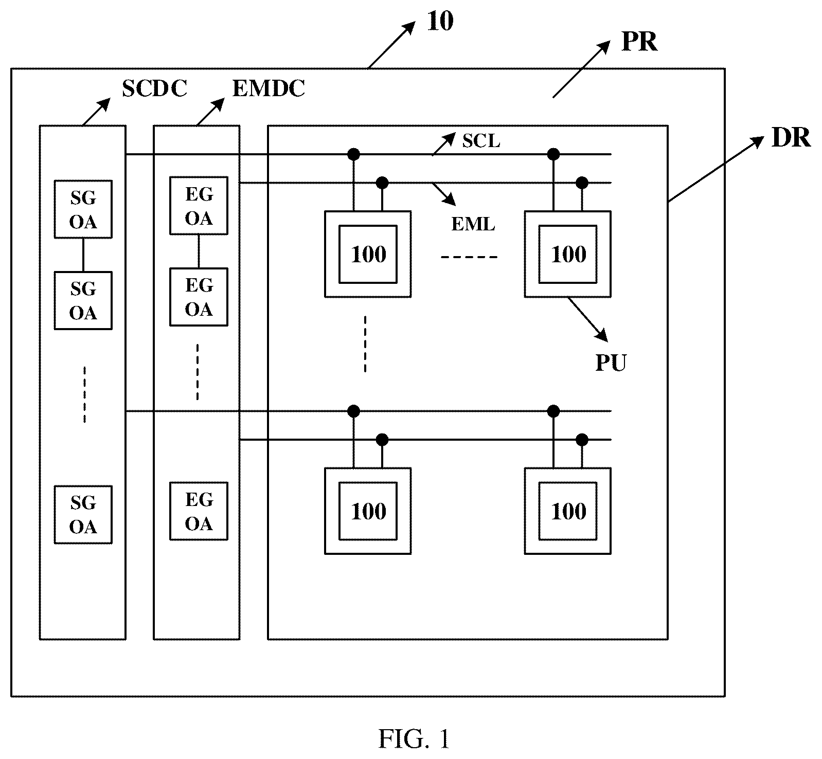
illustrates a display panel 10 , and the display panel 10 includes a display region DR and a peripheral region PR surrounding the display region DR. For example, a plurality of pixel units PU arranged in array are provided in the display region DR, and each pixel unit PU includes a pixel circuit 100 . For example, the pixel circuit 100 is used to drive the pixel unit PU to emit light. For example, a light-emission control scan driving circuit EMDC and a switch control scan driving circuit SCDC are provided in the peripheral region PR.
It should be noted that the sizes of the display region DR and the peripheral region PR illustrated in are only schematic, and the embodiments of the present disclosure do not limit the sizes of the display region DR and the peripheral region PR.
For example, the light-emission control scan driving circuit EMDC includes a plurality of cascaded light-emission control shift register units EGOA, and is configured to sequentially output light-emission control pulse signals, for example, the light-emission control pulse signals are provided to the pixel units PU to control the pixel units PU to emit light. For example, the light-emission control scan driving circuit EMDC is electrically connected to a pixel unit PU through a light-emission control line EML, so that a light-emission control pulse signal can be supplied to the pixel unit PU through the light-emission control line EML. For example, the light-emission control pulse signal is supplied to the light-emission control sub-circuit in the pixel circuit 100 in the pixel unit PU, so that the light-emission control pulse signal can control the light-emission control sub-circuit to be turned on or turned off. The pixel circuit 100 and the light-emission control sub-circuit will be described below, and are not repeated here for simplicity.
For example, the switch control scan driving circuit SCDC includes a plurality of cascaded switch control shift register units SGOA, and is configured to sequentially output switch control pulse signals, for example, the switch control pulse signals are provided to the pixel units PU to control the pixel units PU to perform operations such as data writing or threshold voltage compensation. For example, the switch control scan driving circuit SCDC is electrically connected to a pixel unit PU through a switch control line SCL, so that a switch control pulse signal can be supplied to the pixel unit PU through the switch control line SCL. For example, the switch control pulse signal is supplied to the data writing sub-circuit in the pixel circuit 100 in the pixel unit PU, so that the switch control pulse signal can control the data writing sub-circuit to be turned on or turned off. The data writing sub-circuit will described below, and is not repeated here for simplicity.
For example, in some embodiments, the pixel circuit 100 in may adopt the circuit structure illustrated in , and the working principle of the pixel circuit 100 illustrated in are described below in combination with to D .
As illustrated in , the pixel circuit 100 includes a driving sub-circuit 110 , a data writing sub-circuit 120 , a compensation sub-circuit 130 , a light-emission control sub-circuit 140 , a first reset sub-circuit 150 , a second reset sub-circuit 160 , and a light-emitting element D 1 .
The driving sub-circuit 110 is configured to control a driving current for driving the light-emitting element D 1 to emit light. For example, the driving sub-circuit 110 may be implemented as a first transistor T 1 , a gate electrode of the first transistor T 1 is connected to a first node N 1 , a first electrode of the first transistor T 1 is connected to a second point N 2 , and a second electrode of the first transistor T 1 is connected to a third node N 3 .
The data writing sub-circuit 120 is configured to write a data signal DATA to the driving sub-circuit 110 in response to a scan signal GATE (an example of the switch control pulse signal), for example, write the data signal DATA to the second node N 2 . For example, the data writing sub-circuit 120 may be implemented as a second transistor T 2 , a gate electrode of the second transistor T 2 is configured to receive the scan signal GATE, a first electrode of the second transistor T 2 is configured to receive the data signal DATA, and a second electrode of the second transistor T 2 is connected to the second node N 2 .
The compensation sub-circuit 130 is configured to store the data signal DATA that is written therein, and compensate the driving sub-circuit 110 in response to the scan signal GATE. For example, the compensation sub-circuit 130 may be implemented to include a third transistor T 3 and a storage capacitor CST. A gate electrode of the third transistor T 3 is configured to receive the scan signal GATE, a first electrode of the third transistor T 3 is connected to the third node N 3 , a second electrode of the third transistor T 3 is connected to a first electrode of the storage capacitor CST (that is, the first node N 1 ), and a second electrode of the storage capacitor CST is configured to receive a first voltage VDD.
The light-emission control sub-circuit 140 is configured to apply the first voltage VDD to the driving sub-circuit 110 in response to a light-emission control pulse signal EM 3 and cause the driving current of the driving sub-circuit 110 to be applied to the light-emitting element D 1 . For example, the driving current is applied to the anode of the light-emitting element D 1 . For example, the light-emission control sub-circuit 140 may be implemented to include a fifth transistor T 5 and a sixth transistor T 6 . A gate electrode of the fifth transistor T 5 is configured to receive the light-emission control pulse signal EM 3 , a first electrode of the fifth transistor T 5 is configured to receive the first voltage VDD, and a second electrode of the fifth transistor T 5 is connected to the second node N 2 . A gate electrode of the sixth transistor T 6 is configured to receive the light-emission control pulse signal EM 3 , a first electrode of the sixth transistor T 6 is connected to the third node N 3 , and a second electrode of the sixth transistor T 6 is connected to the light-emitting element D 1 .
The first reset sub-circuit 150 is configured to apply a reset voltage VINT to the driving sub-circuit 110 in response to a reset signal RST (an example of the switch control pulse signal), for example, apply the reset voltage VINT to the first node N 1 . For example, the reset sub-circuit 150 may be implemented as a fourth transistor T 4 , a gate electrode of the fourth transistor T 4 is configured to receive the reset signal RST, a first electrode of the fourth transistor T 4 is configured to receive the reset voltage VINT, and a second electrode of the fourth transistor T 4 is connected to the first node N 1 .
The second reset sub-circuit 160 is configured to apply the reset voltage VINT to the light-emitting element D 1 in response to the reset signal RST, for example, apply the reset voltage VINT to the anode of the light-emitting element D 1 , so that the light-emitting element D 1 can be reset. For example, the second reset sub-circuit 160 may be implemented as a seventh transistor T 7 , a gate electrode of the seventh transistor T 7 is configured to receive the reset signal RST, a first electrode of the seventh transistor T 7 is configured to receive the reset voltage VINT, and a second electrode of the seventh transistor T 7 is connected to the light-emitting element D 1 .
For example, the light-emitting element D 1 may adopt an OLED, and is configured to be connected to the light-emitting control sub-circuit 140 and the second reset sub-circuit 160 , and to receive a second voltage VSS. For example, the light-emitting element OLED may be of various types, such as top emission, bottom emission, etc., and may emit red light, green light, blue light, or white light, etc. The embodiments of the present disclosure are not limited in this aspect. For example, the anode of the OLED is connected to the second electrode of the sixth transistor T 6 and the second electrode of the seventh transistor T 7 , and the cathode of the OLED is configured to receive the second voltage VSS.
It should be noted that, in the embodiments of the present disclosure, for example, the second voltage VSS is maintained at a low level, and the first voltage VDD is maintained at a high level. In the descriptions of the embodiments of the present disclosure, the first node, the second node, and the third node do not represent components that actually exist, but represent meeting points of the related electrical connections in the circuit diagram. The following embodiments are the same and will not be repeated here.
In addition, each of the transistors adopted in the embodiments of the present disclosure may be a thin film transistor, a field effect transistor or other switching component having the same characteristics. In the embodiments of the present disclosure, the thin film transistor is taken as an example for description. The source electrode and drain electrode of the transistor used here may be structurally symmetrical, so that the source electrode and the drain electrode may be structurally indistinguishable. In the embodiments of the present disclosure, in order to distinguish the two electrodes of the transistor except the gate electrode, one electrode is directly described as the first electrode, and the other electrode is described as the second electrode.
The transistors in the pixel circuit 100 illustrated in are all described by using P-type transistors as an example. In this case, the first electrode may be a source electrode, and the second electrode may be a drain electrode. The embodiments of the present disclosure include but are not limited to the configuration of . For example, the transistors in the pixel circuit 100 may also adopt a mixture of P-type transistors and N-type transistors, as long as the port polarities of the selected types of transistors are correspondingly connected according to the port polarities of the corresponding transistors in the embodiments of the present disclosure.
The working principle of the pixel circuit 100 illustrated in is described below with reference to the timing diagram illustrated in and the schematic diagrams illustrated in A to C . As illustrated in , there are included three stages, which are a initialization stage 1 , a data writing and compensation stage 2 , and a light-emitting stage 3 , and illustrates the timing waveform of each signal in each stage.
It should be noted that, A is a schematic diagram in the case where the pixel circuit 100 illustrated in is in the initialization stage 1 , B is a schematic diagram in the case where the pixel circuit 100 illustrated in is in the data writing and compensation stage 2 , and C is a schematic diagram in the case where the pixel circuit 100 illustrated in is in the light-emitting stage 3 . In addition, the transistors marked with dashed lines in A to C indicate that the transistors are in a turn-off state in the corresponding stage. The transistors illustrated in A to C are all described by using P-type transistors as an example, that is, each transistor is turned on when the gate electrode is connected to a low level, and is turned off when the gate electrode is connected to a high level.
In the initialization stage 1 , as illustrated in and A , the reset signal RST is at a low level, and the fourth transistor T 4 and the seventh transistor T 7 are turned on. The fourth transistor T 4 that is turned on may apply the reset voltage VINT (a low-level signal, for example, may be grounded or other low-level signal) to the gate electrode of the first transistor T 1 , thereby completing the reset of the first transistor T 1 . The reset voltage VINT is applied to the anode of the light-emitting element D 1 through the seventh transistor T 7 that is turned on, thereby completing the reset of the light-emitting element D 1 . Resetting the light-emitting element D 1 in the initialization stage 1 can improve the contrast.
In the data writing and compensation stage 2 , as illustrated in and B , the scan signal GATE is at a low level, the second transistor T 2 and the third transistor T 3 are turned on, and the first transistor T 1 maintains the turn-on state of the previous stage.
The data signal DATA charges the first node N 1 (that is, charges the storage capacitor CST) through the second transistor T 2 , the first transistor T 1 , and the third transistor T 3 that are turned on, that is, the level of the first node N 1 becomes larger. It is easy to understand that the level of the second node N 2 is maintained at the level Vdata of the data signal DATA, and according to the characteristics of the first transistor T 1 , when the level of the first node N 1 increases to Vdata+Vth, the first transistor T 1 is turned off, and the charging process ends. It should be noted that, Vdata represents the level of the data signal DATA, and Vth represents the threshold voltage of the first transistor T 1 . Because the first transistor T 1 is described here by using a P-type transistor as an example, the threshold voltage Vth is a negative value.
After the data writing and compensation stage 2 , the level of the first node N 1 and the level of the third node N 3 are both at Vdata+Vth, which means that the voltage information with the data signal DATA and the threshold voltage Vth is stored in the storage capacitor CST, in order to provide grayscale display data and compensate the threshold voltage of the first transistor T 1 during the subsequent light-emitting stage.
In the light-emitting stage 3 , as illustrated in and C , the light-emission control pulse signal EM 3 is at a low level, and the fifth transistor T 5 and the sixth transistor T 6 are turned on; meanwhile, because the level of the first node N 1 remains at Vdata+Vth, and the level of the second node N 2 is the first voltage VDD, the first transistor T 1 also remains in turn-on state in this stage.
As illustrated in C , in the light-emitting stage 4 , the anode and cathode of the light-emitting element D 1 are connected to the first voltage VDD (high level) and the second voltage VSS (low level) respectively, so that the light-emitting element D 1 emits light under the action of the driving current flowing through the first transistor T 1 .
Specifically, the value of the driving current IDI flowing through the light-emitting element D 1 may be obtained according to the following formula:
I D 1 = K ( V GS - Vth ) 2 = K [ ( Vdata + Vth - VDD ) - Vth ] 2 = K ( Vdata - VDD ) 2
In the above formula, Vth represents the threshold voltage of the first transistor T 1 , V GS represents the voltage between the gate electrode and the source electrode of the first transistor T 1 , and K is a constant value. It can be seen from the above formula that the driving current IDI flowing through the light-emitting element D 1 is no longer related to the threshold voltage Vth of the first transistor T 1 , but only related to the voltage Vdata of the data signal DATA that controls the light-emission grayscale of the pixel circuit 100 , so that the compensation of the pixel circuit 100 may be realized, which solves the problem of the threshold voltage drift caused by the process and long-term operation of the driving transistor (the first transistor T 1 in the embodiment of the present disclosure), and eliminates the influence of the threshold voltage drift on the driving current I D1 , thereby improving the effect of the display panel that adopts the pixel circuit 100 .
As can be seen from the above, the pixel circuit 100 illustrated in emits light during the light-emitting stage 3 , for example, the light-emission brightness of the pixel circuit 100 may be adjusted by controlling the time maintained by the light-emitting stage 3 , that is, the light-emission brightness of the pixel unit PU that adopts the pixel circuit 100 may be adjusted by controlling the pulse width of the light-emission control pulse signal.
The light-emission control scan driving circuit EMDC illustrated in includes a plurality of cascaded light-emission control shift register units EGOA. For example, each stage of the plurality of cascaded light-emission control shift register units EGOA may adopt the circuit structure illustrated in . The working principle of the light-emission control shift register unit EGOA illustrated in is described below with reference to to E .
As illustrated in , the light-emission control shift register unit EGOA includes 10 transistors (first transistor M 1 , second transistor M 2 , . . . , tenth transistor M 10 ) and three capacitors (first capacitor C 1 , second capacitor C 2 , and third capacitor C 3 ). For example, in the case where a plurality of light-emission control shift register units EGOA are cascaded, the first electrode of the first transistor M 1 in the first-stage light-emission control shift register unit EGOA is configured to receive a start signal ESTV, while the first electrode of the first transistor M 1 in any one of the light-emission control shift register units of other stages is connected to the light-emission control shift register unit of a preceding stage, which is before the any one of the light-emission control shift register units of other stages, to receive the light-emission control pulse signal EM output by the light-emission control shift register unit of the preceding stage. In addition, CK in and represents a first clock signal, and CB represents a second clock signal. For example, the first clock signal CK and the second clock signal CB may both adopt a pulse signal with a duty cycle greater than 50%; VGH represents a third voltage, for example, the third voltage is maintained at a high level, VGL represents a fourth voltage, for example, the fourth voltage is maintained at a low level, and N 1 , N 2 , N 3 , and N 4 represent the first node, the second node, the third node, and the fourth node, respectively. For the connection relationship between each transistor and each capacitor in , reference may be made to that illustrated in , and details are not repeated here.
The transistors in the light-emission control shift register unit EGOA illustrated in are all described by using P-type transistors as an example. In this case, the first electrode may be a source electrode, and the second electrode may be a drain electrode. The embodiments of the present disclosure include but are not limited to the configuration of . For example, the transistors in the light-emission control shift register unit EGOA may also adopt a mixture of P-type transistors and N-type transistors, as long as the port polarities of the selected types of transistors are correspondingly connected according to the port polarities of the corresponding transistors in the embodiments of the present disclosure.
The working principle of the light-emission control shift register unit EGOA illustrated in is described below with reference to the timing diagram illustrated in and the schematic diagrams illustrated in A to E . As illustrated in , five stages are included, which are a first stage P 1 , a second stage P 2 , a third stage P 3 , a fourth stage, P 4 and a fifth stage P 5 , and illustrates the timing waveform of each signal in each stage.
It should be noted that, A is a schematic diagram in the case where the light-emission control shift register unit EGOA illustrated in is in the first stage P 1 , B is a schematic diagram in the case where the light-emission control shift register unit EGOA illustrated in is in the second stage P 2 , C is a schematic diagram in the case where the light-emission control shift register unit EGOA illustrated in is in the third stage P 3 , D is a schematic diagram in the case where the light-emission control shift register unit EGOA illustrated in is in the fourth stage P 4 , and E is a schematic diagram in the case where the light-emission control shift register unit EGOA illustrated in is in the fifth stage P 5 . In addition, the transistors marked with dashed lines in A to E indicate that the transistors are in a turn-off state in the corresponding stage. The transistors illustrated in A to E are all described by using P-type transistors as an example, that is, each transistor is turned on when the gate electrode is connected to a low level, and is turned off when the gate electrode is connected to a high level.
In the first stage P 1 , as illustrated in and A , the first clock signal CK is at a low level, so the first transistor M 1 and the third transistor M 3 are turned on, and the first transistor M 1 that is turned on transmits the high-level start signal ESTV to the first node N 1 , so that the level of the first node N 1 becomes a high level, and the second transistor M 2 , the eighth transistor M 8 , and the tenth transistor M 10 are turned off. In addition, the third transistor M 3 that is turned on transmits the low-level fourth voltage VGL to the second node N 2 , so that the level of the second node N 2 becomes a low level, so the fifth transistor M 5 and the sixth transistor M 6 are turned on. Because the second clock signal CB is at a high level, the seventh transistor M 7 is turned off. In addition, due to the storage effect of the third capacitor C 3 , the level of the fourth node N 4 may be maintained at a high level, so that the ninth transistor M 9 is turned off. In the first stage P 1 , because both the ninth transistor M 9 and the tenth transistor M 10 are turned off, the light-emission control pulse signal EM output by the light-emission control shift register unit EGOA remains at the previous low level.
In the second stage P 2 , as illustrated in and B , the second clock signal CB is at a low level, so the fourth transistor M 4 and the seventh transistor M 7 are turned on. Because the first clock signal CK is at a high level, the first transistor M 1 and the third transistor M 3 are turned off. Due to the storage effect of the first capacitor C 1 , the second node N 2 may continue to maintain the low level of the previous stage, and the fifth transistor M 5 and the sixth transistor M 6 are turned on. The high-level third voltage VGH is transmitted to the first node N 1 through the fifth transistor M 5 and the fourth transistor M 4 that are turned on, so that the level of the first node N 1 continues to maintain the high level of the previous stage, so the second transistor M 2 , the eighth transistor M 8 , and the tenth transistor M 10 are turned off. In addition, the low-level second clock signal CB is transmitted to the fourth node N 4 through the sixth transistor M 6 and the seventh transistor M 7 that are turned on, so that the level of the fourth node N 4 becomes a low level, so the ninth transistor M 9 is turned on, and the ninth transistor M 9 that is turned on outputs the high-level third voltage VGH, so the light-emission control pulse signal EM output by the light-emission control shift register unit EGOA in the second stage P 2 is at a high level.
In the third stage P 3 , as illustrated in and C , the first clock signal CK is at a low level, so the first transistor M 1 and the third transistor M 3 are turned on. The second clock signal CB is at a high level, so the fourth transistor M 4 and the seventh transistor M 7 are turned off. Due to the storage effect of the third capacitor C 3 , the level of the fourth node N 4 may maintain the low level of the previous stage, so that the ninth transistor M 9 remains in the turn-on state, and the ninth transistor M 9 that is turned on outputs the high-level third voltage VGH, so the light-emission control pulse signal EM output by the light-emission control shift register unit EGOA in the third stage P 3 is still at a high level.
In the fourth stage P 4 , as illustrated in and D , the first clock signal CK is at a high level, so the first transistor M 1 and the third transistor M 3 are turned off. The second clock signal CB is at a low level, so the fourth transistor M 4 and the seventh transistor M 7 are turned on. Due to the storage effect of the second capacitor C 2 , the level of the first node N 1 maintains the high level of the previous stage, so that the second transistor M 2 , the eighth transistor M 8 , and the tenth transistor M 10 are turned off. Due to the storage effect of the first capacitor C 1 , the second node N 2 continues to maintain the low level of the previous stage, so that the fifth transistor M 5 and the sixth transistor M 6 are turned on. In addition, the low-level second clock signal CB is transmitted to the fourth node N 4 through the sixth transistor M 6 and the seventh transistor M 7 that are turned on, so that the level of the fourth node N 4 becomes a low level, so the ninth transistor M 9 is turned on, and the ninth transistor M 9 that is turned on outputs the high-level third voltage VGH, so the light-emission control pulse signal EM output by the light-emission control shift register unit EGOA in the second stage P 2 is still at a high level.
In the fifth stage P 5 , as illustrated in and E , the first clock signal CK is at a low level, so the first transistor M 1 and the third transistor M 3 are turned on. The second clock signal CB is at a high level, so the fourth transistor M 4 and the seventh transistor M 7 are turned off. The first transistor M 1 that is turned on transmits the low-level start signal ESTV to the first node N 1 , so that the level of the first node N 1 becomes a low level, so the second transistor M 2 , the eighth transistor M 8 , and the tenth transistor M 10 is turned on. The second transistor M 2 that is turned on transmits the low-level first clock signal CK to the second node N 2 , so that the level of the second node N 2 may be further lowered, the second node N 2 continues to maintain the low level of the previous stage, and the fifth transistor M 5 and the sixth transistor M 6 are turned on. In addition, the eighth transistor M 8 that is turned on transmits the high-level third voltage VGH to the fourth node N 4 , so that the level of the fourth node N 4 becomes a high level, so the ninth transistor M 9 is turned off. The tenth transistor M 10 that is turned on outputs the low-level fourth voltage VGL, so the light-emission control pulse signal EM output by the light-emission control shift register unit EGOA in the fifth stage P 5 becomes a low-level.
As described above, the pulse width of the light-emission control pulse signal EM output by the light-emission control shift register unit EGOA is related to the pulse width of the start signal ESTV, for example, the two are equal. Therefore, the pulse width of the light-emission control pulse signal EM output by the light-emission control shift register unit EGOA may be adjusted by adjusting the pulse width of the start signal ESTV, so that the light-emission time of the corresponding pixel unit PU may be adjusted, and thus the light-emission of the pixel unit PU is adjusted.
Continuing to return to and , in order to drive the pixel circuit 100 in the pixel unit PU to work normally, it is necessary to provide the light-emission control pulse signal and the switch control pulse signal (for example, the scan signal GATE, the reset signal RST) to the pixel circuit 100 . For example, the light-emission control pulse signals may be sequentially output through the light-emission control scan driving circuit EMDC to respectively control the light-emission control sub-circuits in the pixel circuits 100 in the rows of pixel units PU. For example, the switch control pulse signals may be sequentially output through the switch control scan driving circuit SCDC to respectively control the data writing sub-circuits, the compensation sub-circuits, and the reset sub-circuits in the pixel circuits 100 in the rows of pixel units PU. It should be noted that the implementation of the switch control shift register unit SGOA is not limited in the embodiments of the present disclosure, as long as it can output the above-mentioned switch control pulse signal.
illustrates a foldable display panel 10 , and the display panel 10 includes a first display region DR 1 , a second display region DR 2 , and a peripheral region PR surrounding the first display region DR 1 and the second display region DR 2 . For example, rows of pixel units PU arranged in array are provided in the first display region DR 1 and the second display region DR 2 , which are not illustrated in . For example, similar to the display panel 10 illustrated in , the light-emission control scan driving circuit EMDC and the switch control scan driving circuit SCDC may be provided in the peripheral region PR, which is not illustrated in .
As illustrated in , the display panel 10 can be bent along a folding axis 600 , and the display panel 10 may be divided into a primary screen including the first display region DR 1 and a secondary screen including the second display region DR 2 along the folding axis 600 . For example, in the case where the display panel 10 is in a flat state, both the primary screen and the secondary screen can be displayed; while in the case where the display panel 10 is in a folded state, for example, only one of the primary screen and the secondary screen can be displayed, or, both the primary screen and the secondary screen can be displayed at the same time. The following embodiments are described by taking the case where the primary screen is displayed while the secondary screen is not displayed in the folded state as an example, and details are not described herein again.
After the display panel 10 is used for a long time, because the light-emission time of the primary screen is longer than the light-emission time of the secondary screen, the attenuation of the light-emitting element in the pixel unit PU in the primary screen (that is, the first display region DR 1 ) is stronger than the attenuation of the light-emitting element in the pixel unit PU in the secondary screen (that is, the second display region DR 2 ), so that in the case where both the primary screen and the secondary screen of the display panel 10 need to be displayed, for example, the same grayscale voltage value is input to the primary screen and the secondary screen, the brightness of the primary screen may be less than the brightness of the secondary screen, thereby causing the problem of the bright-and-dark screen illustrated in .
For example, in the case where the display panel 10 illustrated in includes N rows of pixel units PU, the light-emission control scan driving circuit EMDC for the display panel 10 illustrated in is illustrated in . As illustrated in , the light-emission control scan driving circuit EMDC includes a plurality of cascaded light-emission control shift register units EGOA. For example, the EGOA may adopt the circuit structure illustrated in . As illustrated in , the first-stage light-emission control shift register unit EGOA( 1 ) is configured to receive the start signal ESTV and output the light-emission control pulse signal EM( 1 ) for the first row of pixel units PU. In the following description, the number in parenthesis indicate the corresponding number of the stage of the light-emission control shift register unit or the number of the row of the pixel units corresponding to the light-emission control pulse signal, which is not repeated. For example, except the first-stage light-emission control shift register unit EGOA( 1 ), any one of the light-emission control shift register units of other stages receives the light-emission control pulse signal output by the light-emission control shift register unit of a preceding stage which is before the any one of the light-emission control shift register units of other stages.
As described above, in the case where the display panel 10 illustrated in adopts the light-emission control scan driving circuit EMDC illustrated in , for example, in the case where the display panel 10 is in the folded state and only the primary screen is displayed, it is necessary to write the grayscale voltage value corresponding to a black frame to the secondary screen at this time, that is, even if the secondary screen does not need to be displayed, the data signal DATA still needs to be provided to the secondary screen. Moreover, the pixel circuit 100 in the pixel unit PU in the secondary screen still needs to store the data signal DATA by the storage capacitor (such as the storage capacitor CST in ), so the secondary screen may be affected by the leakage of the storage capacitor, especially, this effect is more severer when displaying low grayscale, which may cause the problem of mura (uneven display brightness).
The display panel, the display device, and the driving method provided by the embodiments of the present disclosure are proposed to solve the above problems, and the embodiments and examples of the present disclosure are described in detail below with reference to the drawings.
At least one embodiment of the present disclosure provides a display panel, as illustrated in A , the display panel 10 includes a plurality of display regions, a peripheral region PR surrounding the plurality of display regions, a plurality of light-emission control scan driving circuits provided in the peripheral region PR, a first start signal line ESL 1 , and a second start signal line ESL 2 , and the first start signal line ESL 1 is different from the second start signal line ESL 2 .
For example, in some embodiments, the plurality of display regions include a first display region DR 1 and a second display region DR 2 which are side by side but not overlapped with each other, the first display region DR 1 includes rows of first pixel units PU 1 arranged in array, and the second display region DR 2 includes rows of second pixel units PU 2 arranged in array. For example, the rows of first pixel units PU 1 in the first display region DR 1 are arranged continuously, and the rows of second pixel units PU 2 in the second display region DR 2 are arranged continuously.
For example, in some embodiments, the plurality of light-emission control scan driving circuits include a first light-emission control scan driving circuit EMDC 1 for controlling the rows of first pixel units PU 1 to emit light, and a second light-emission control scan driving circuit EMDC 2 for controlling the rows of second pixel units PU 2 to emit light.
The first start signal line ESL 1 is electrically connected to the first light-emission control scan driving circuit EMDC 1 , and is configured to provide a first start signal ESTV 1 to the first light-emission control scan driving circuit EMDC 1 , and the second start signal line ESL 2 is electrically connected to the second light-emission control scan driving circuit EMDC 2 , and is configured to provide a second start signal ESTV 2 to the second light-emission control scan driving circuit EMDC 2 .
It should be noted that the sizes of the first display region DR 1 , the second display region DR 2 , and the peripheral region PR illustrated in A are only schematic, and the embodiments of the present disclosure do not limit the sizes of the first display region DR 1 , the second display region DR 2 , and the peripheral region PR.
As illustrated in A , the first start signal line ESL 1 is electrically connected to the first light-emission control scan driving circuit EMDC 1 to provide the first start signal ESTV 1 , and the first light-emission control scan driving circuit EMDC 1 can be triggered by the first start signal ESTV 1 to sequentially output a first light-emission control pulse signal EM 1 . For example, the first light-emission control pulse signal EM 1 is provided to the first pixel unit PU 1 in the first display region DR 1 , for example, to control the light-emission control sub-circuit in the pixel circuit in the first pixel unit PU 1 .
As illustrated in A , the second start signal line ESL 2 is electrically connected to the second light-emission control scan driving circuit EMDC 2 to provide the second start signal ESTV 2 , and the second light-emission control scan driving circuit EMDC 2 can be triggered by the second start signal ESTV 2 to sequentially output a second light-emission control pulse signal EM 2 . For example, the second light-emission control pulse signal EM 2 is provided to the second pixel unit PU 2 in the second display region DR 2 , for example, to control the light-emission control sub-circuit in the pixel circuit in the second pixel unit PU 2 .
In the display panel 10 provided by the embodiment of the present disclosure, by setting the first start signal line ESL 1 , the first light-emission control scan driving circuit EMDC 1 is triggered by the first start signal ESTV 1 to output the first light-emission control pulse signal EM 1 , so as to control the rows of first pixel units PU 1 in the first display region DR 1 to emit light; and by setting the second start signal line ESL 2 , the second light-emission control scan driving circuit EMDC 2 is triggered by the second start signal ESTV 2 to output the second light-emission control pulse signal EM 2 , so as to control the rows of second pixel units PU 2 in the second display region DR 2 to emit light. Compared to the display panel that uses only one start signal line, the display panel 10 provided by the embodiment of the present disclosure can implement independent control of the plurality of display regions by setting a plurality of separate start signal lines.
For example, in some embodiments, the display panel 10 illustrated in A may be a foldable display panel and includes a folding axis 600 , and the first display region DR 1 and the second display region DR 2 are divided along the folding axis 600 . The foldable display panel 10 according to the embodiment of the present disclosure may be foldable in various ways, for example, by a flexible region, hinge, etc. of the display panel 10 , and the position of the flexible region or the hinge corresponds to the folding axis 600 , the embodiments of the present disclosure do not limit the way to achieve folding.
For example, the first display region DR 1 of the display panel 10 illustrated in A corresponds to the primary screen, and the second display region DR 2 corresponds to the secondary screen. For example, in the case where only the primary screen (that is, the first display region DR 1 ) is required for display and the secondary screen (that is, the second display region DR 2 ) is not required for display, the first start signal ESTV 1 and the second start signal ESTV 2 that are different may be respectively provided through the first start signal line ESL 1 and the second start signal line ESL 2 , so as to control the first light-emission control scan driving circuit EMDC 1 to sequentially output the first light-emission control pulse signals EM 1 , and the first light-emission control pulse signals EM 1 can control the rows of first pixel units PU 1 in the first display region DR 1 to perform display; and control the second light-emission control scan driving circuit EMDC 2 to output the second light-emission control pulse signal EM 2 with a fixed level, and the second light-emission control pulse signal EM 2 can control the rows of second pixel units PU 2 in the second display region DR 2 not to emit light, thereby displaying the black frame.
For another example, in the case where only the secondary screen (that is, the second display region DR 2 ) is required for display and the primary screen (that is, the first display region DR 1 ) is not required for display, the first start signal ESTV 1 and the second start signal ESTV 2 that are different may be respectively provided through the first start signal line ESL 1 and the second start signal line ESL 2 , so as to control the second light-emission control scan driving circuit EMDC 2 to sequentially output the second light-emission control pulse signals EM 2 , and the second light-emission control pulse signals EM 2 can control the rows of second pixel units PU 2 in the second display region DR 2 to perform display; and control the first light-emission control scan driving circuit EMDC 1 to output the first light-emission control pulse signal EM 1 with a fixed level, and the first light-emission control pulse signal EM 1 can control the rows of first pixel units PU 1 in the first display region DR 1 not to emit light, thereby displaying the black frame.
For example, the display panel 10 illustrated in A may be a foldable display panel. In the case where the display panel 10 is in the folded state and the primary screen is displayed while the secondary screen is not displayed, the rows of second pixel units PU 2 in the second display region DR 2 may be made not to display, so that the data signals DATA no longer need to be provided to the secondary screen, and thus the power consumption of the display panel may be reduced. In addition, because the pixel circuit 100 in the second pixel unit PU 2 in the second display region DR 2 no longer requires the storage capacitor to store the data signals DATA, the problem of mura due to leakage of the storage capacitor may also be eliminated or avoided.
It should be noted that examples of the first start signal ESTV 1 and the second start signal ESTV 2 applied in the case where the display panel 10 is in the folded state are described below, and not repeated here.
In addition, it should be noted that, in the display panel 10 provided by the embodiment of the present disclosure, the size of the first pixel unit PU 1 and the size of the second pixel unit PU 2 may be the same, in this case, the resolution of the first display region DR 1 is the same as the resolution of the second display region DR 2 ; the size of the first pixel unit PU 1 and the size of the second pixel unit PU 2 may also be different, in this case, the resolution of the first display region DR 1 and the resolution of the second display region DR 2 are different. For example, in the case where the primary screen is needed to display content with a higher resolution, the first pixel unit PU 1 may be smaller than the second pixel unit PU 2 .
In the display panel 10 provided by some embodiments of the present disclosure, as illustrated in A , the first start signal line ESL 1 and the second start signal line ESL 2 are provided at a side, close to the plurality of display regions (the first display region DR 1 and the second display region DR 2 ), of the plurality of light-emission control scan driving circuits (the first light-emission control scan driving circuit EMDC 1 and the second light-emission control scan driving circuit EMDC 2 ), and the extending direction of the first start signal line ESL 1 and the extending direction of the second start signal line ESL 2 are the same.
It should be noted that, the embodiments of the present disclosure are not limited to the above situation. For example, as illustrated in B , the first start signal line ESL 1 and the second start signal line ESL 2 may also be provided at a side, away from the plurality of display regions (the first display region DR 1 and the second display region DR 2 ), of the plurality of light-emission control scan driving circuits (the first light-emission control scan driving circuit EMDC 1 and the second light-emission control scan driving circuit EMDC 2 ).
For example, in the embodiments of the present disclosure, an end, which is close to the last row of second pixel units PU 2 in the second display region DR 2 , of the display panel is called the near end (for example, an end close to the control circuit), and an end, which is close to the first row of first pixel units PU 1 in the first display region DR 1 , of the display panel is called the far end (for example, an end away from the control circuit). For example, in the display panel 10 provided by some embodiments of the present disclosure, as illustrated in A , the first start signal line ESL 1 and the second start signal line ESL 2 are both extended from the near end to the far end.
In the case where the first display region DR 1 in the display panel 10 illustrated in A includes N rows of first pixel units PU 1 (N is an integer greater than 1), and the second display region DR 2 includes N rows of second pixel units PU 2 , illustrates an example of the first light-emission control scan driving circuit EMDC 1 , the second light-emission control scan driving circuit EMDC 2 , the first start signal line ESL 1 , and the second start signal line ESL 2 in the display panel 10 illustrated in A .
As illustrated in , the first light-emission control scan driving circuit EMDC 1 includes a plurality of cascaded first light-emission control shift register units EGOA 1 , for example, includes a first-stage first light-emission control shift register unit EGOA 1 ( 1 ), a second-stage first light-emission control shift register unit EGOA 1 ( 2 ), . . . , an Nth-stage first light-emission control shift register unit EGOA 1 (N). Each stage of the plurality of cascaded first light-emission control shift register units EGOA 1 includes a first output electrode OE 1 , and a plurality of first output electrodes OE 1 of the plurality of cascaded first light-emission control shift register units EGOA 1 are configured to sequentially output the first light-emission control pulse signals EM 1 . For example, the first-stage first light-emission control shift register unit EGOA 1 ( 1 ) outputs the first light-emission control pulse signal EM 1 ( 1 ), for example, the first light-emission control pulse signal EM 1 ( 1 ) is provided to the first row of first pixel units PU 1 in the first display region DR 1 to control the first row of first pixel units PU 1 to emit light.
As illustrated in , the second light-emission control scan driving circuit EMDC 2 includes a plurality of cascaded second light-emission control shift register units EGOA 2 , for example, includes a first-stage second light-emission control shift register unit EGOA 2 ( 1 ), a second-stage second light-emission control shift register unit EGOA 2 ( 2 ), . . . , an Nth-stage second light-emission control shift register unit EGOA 2 (N). Each stage of the plurality of cascaded second light-emission control shift register units EGOA 2 includes a second output electrode OE 2 , and a plurality of second output electrodes OE 2 of the plurality of cascaded second light-emission control shift register units EGOA 2 are configured to sequentially output the second light-emission control pulse signals EM 2 . For example, the first-stage second light-emission control shift register unit EGOA 2 ( 1 ) outputs the second light-emission control pulse signal EM 2 ( 1 ), for example, the second light-emission control pulse signal EM 2 ( 1 ) is provided to the first row of second pixel units PU 2 in the second display region DR 2 to control the first row of second pixel units PU 2 to emit light.
For example, the first start signal line ESL 1 is at least partially overlapped with each of the plurality of first output electrodes OE 1 , and is at least partially overlapped with each of the plurality of second output electrodes OE 2 ; and the second start signal line ESL 2 is at least partially overlapped with each of the plurality of first output electrodes OE 1 , and is at least partially overlapped with each of the plurality of second output electrodes OE 2 .
It should be noted that, the widths and lengths of the first output electrode OE 1 and the second output electrode OE 2 illustrated in are only schematic, and the lengths and the widths of the first start signal line ESL 1 and the second start signal line ESL 2 are only schematic, and the embodiments of the present disclosure are not limited in this aspect.
In the display panel provided by some embodiments of the present disclosure, the first output electrode OE 1 is at least partially overlapped with the first start signal line ESL 1 and the second start signal line ESL 2 , and the second output electrode OE 2 is at least partially overlapped with the first start signal line ESL 1 and the second start signal line ESL 2 ; thus, the parasitic capacitances generated between the first output electrode OE 1 and the first start signal line ESL 1 , and the second start signal line ESL 2 , and the parasitic capacitances generated between the second output electrode OE 2 and the first start signal line ESL 1 , and the second start signal line ESL 2 are approximately equal; thus, the signal delay caused by the first start signal ESTV 1 , and the second start signal ESTV 2 to the first light-emission control pulse signal EM 1 , and the signal delay caused by the first start signal ESTV 1 , and the second start signal ESTV 2 to the second light-emission control pulse signal EM 2 are approximately equal; thus, the problem of split-screen of primary screen and secondary screen of the display panel can be eliminated or avoided.
For example, as illustrated in , in the display panel 10 provided by some embodiments of the present disclosure, the length of the first start signal line ESL 1 along the extending direction of the first start signal line ESL 1 is the first length, the length of the second start signal line ESL 2 along the extending direction of the second start signal line ESL 2 is the second length, and the difference between the first length and the second length is less than a predetermined error value. For example, the predetermined error value is from 1 μm to 10 μm, for example, the first length and the second length may be made equal.
For example, in order to make the first length and the second length equal, the extending direction of the first start signal line ESL 1 and the extending direction of the second start signal line ESL 2 may be parallel to each other, so that the extending direction of the first output electrode OE 1 and the extending direction of the second output electrode OE 2 are parallel to each other, and the extending direction of the first start signal line ESL 1 is perpendicular to the extending direction of the first output electrode OE 1 . In this way, the problem of split-screen display of the display panel can be further eliminated or avoided.
For example, as illustrated in A , in some embodiments, the scanning direction of the first light-emission control scan driving circuit EMDC 1 is the same as the scanning direction of the second light-emission control scan driving circuit EMDC 2 , and the extending direction of the first start signal line ESL 1 and the extending direction of the second start signal line ESL 2 are both parallel to the scanning direction of the first light-emission control scan driving circuit EMDC 1 and the scanning direction of the second light-emission control scan driving circuit EMDC 2 . For example, the scanning direction of the first light-emission control scan driving circuit EMDC 1 is from the first row of first pixel units PU 1 in the first display region DR 1 to the last row of first pixel units PU 1 in the first display region DR 1 , and the scanning direction of the second light-emission control scan driving circuit EMDC 2 is from the first row of second pixel units PU 2 in the second display region DR 2 to the last row of second pixel units PU 2 in the second display region DR 2 .
For example, as illustrated in , in some embodiments, the extending direction of the first start signal line ESL 1 is intersected with the extending direction of the first output electrode OE 1 , and is intersected with the extending direction of the second output electrode OE 2 ; and the extending direction of the second start signal line ESL 2 is intersected with the extending direction of the first output electrode OE 1 , and is intersected with the extending direction of the second output electrode OE 2 .
For example, as illustrated in , in some embodiments, the extending direction of the first start signal line ESL 1 is perpendicular to the extending direction of the first output electrode OE 1 , and is perpendicular to the extending direction of the second output electrode OE 2 ; and the extending direction of the second start signal line ESL 2 is perpendicular to the extending direction of the first output electrode OE 1 , and is perpendicular to the extending direction of the second output electrode OE 2 .
For example, as illustrated in , in the display panel provided by some embodiments, the first-stage first light-emission control shift register unit EGOA 1 ( 1 ) of the plurality of cascaded first light-emission control shift register units EGOA 1 is electrically connected to the first start signal line ESL 1 to receive the first start signal ESTV 1 .
The first-stage second light-emission control shift register unit EGOA 2 ( 1 ) of the plurality of cascaded second light-emission control shift register units EGOA 2 is electrically connected to the second start signal line ESL 2 to receive the second start signal ESTV 2 .
For example, as illustrated in A , in the display panel 10 provided by some embodiments, each stage of the plurality of cascaded first light-emission control shift register units EGOA 1 further includes a first input electrode IE 1 , and the plurality of first output electrodes OE 1 of the plurality of cascaded first light-emission control shift register units EGOA 1 are electrically connected to the rows of first pixel units PU 1 , respectively, to sequentially provide the first light-emission control pulse signals EM 1 . The first input electrode IE 1 of the first-stage first light-emission control shift register unit EGOA 1 ( 1 ) is electrically connected to the first start signal line ESL 1 . In the plurality of cascaded first light-emission control shift register units EGOA 1 , except the first-stage first light-emission control shift register unit EGOA 1 ( 1 ), the first input electrode IE 1 of any one of the first light-emission control shift register units EGOA 1 of other stages is electrically connected to the first output electrode OE 1 of a first light-emission control shift register unit EGOA 1 of a preceding stage before the any one of the first light-emission control shift register units EGOA 1 of other stages.
Each stage of the plurality of cascaded second light-emission control shift register units EGOA 2 further includes a second input electrode IE 2 , and the plurality of second output electrodes OE 2 of the plurality of cascaded second light-emission control shift register units EGOA 2 are electrically connected to the rows of second pixel units PU 2 , respectively, to sequentially provide the second light-emission control pulse signals EM 2 . The second input electrode IE 2 of the first-stage second light-emission control shift register unit EGOA 2 ( 1 ) is electrically connected to the second start signal line ESL 2 . In the plurality of cascaded second light-emission control shift register units EGOA 2 , except the first-stage second light-emission control shift register unit EGOA 2 ( 1 ), the second input electrode IE 2 of any one of the second light-emission control shift register units EGOA 2 of other stages is electrically connected to the second output electrode OE 2 of a second light-emission control shift register unit EGOA 2 of a preceding stage before the any one of the second light-emission control shift register units EGOA 2 of other stages.
For example, in the display panel 10 provided by some embodiments, the first pixel unit PU 1 includes a first pixel circuit. For example, the first pixel circuit may adopt the pixel circuit 100 illustrated in , the embodiments of the present disclosure include but are not limited to this, and the first pixel circuit may also adopt other conventional pixel circuit. The first pixel circuit includes a first light-emission control sub-circuit, and the first light-emission control sub-circuit is configured to receive the first light-emission control pulse signal EM 1 , and control the first pixel unit PU 1 to emit light in response to the first light-emission control pulse signal EM 1 .
For example, the second pixel unit PU 2 includes a second pixel circuit, similarly, the second pixel circuit may also adopt the pixel circuit 100 illustrated in , the embodiments of the present disclosure include but are not limited to this, and the second pixel circuit may also adopt other conventional pixel circuit. The second pixel circuit includes a second light-emission control sub-circuit, and the second light-emission control sub-circuit is configured to receive the second light-emission control pulse signal EM 2 , and control the second pixel unit PU 2 to emit light in response to the second light-emission control pulse signal EM 2 .
As illustrated in A , the display panel 10 provided by some embodiments of the present disclosure further includes a plurality of first light-emission control lines EML 1 and a plurality of second light-emission control lines EML 2 .
The plurality of first light-emission control lines EML 1 are electrically connected to the plurality of first output electrodes OE 1 in one-to-one correspondence, respectively, and the plurality of first light-emission control lines EML 1 are electrically connected to the first light-emission control sub-circuits in the first pixel units PU 1 of different rows in one-to-one correspondence, respectively.
The plurality of second light-emission control lines EML 2 are electrically connected to the plurality of second output electrodes OE 2 in one-to-one correspondence, respectively, and the plurality of second light-emission control lines EML 2 are electrically connected to the second light-emission control sub-circuits in the second pixel units PU 2 of different rows in one-to-one correspondence, respectively.
As illustrated in B , in some embodiments of the present disclosure, the display panel 10 includes a plurality of first light-emission control lines EML 1 and a plurality of second light-emission control lines EML 2 . As illustrated in B , every two adjacent first light-emission control lines EML 1 are electrically connected to same one first output electrode OE 1 of the plurality of first output electrodes OE 1 , that is, the first light-emission control pulse signal EM 1 output by the same first light-emission control shift register unit EGOA 1 is used to control two adjacent rows of first pixel units PU 1 . In this case, the number of the first light-emission control shift register units EGOA 1 included in the first light-emission control scan driving circuit EMDC 1 can be reduced by half, so that the area occupied by the first light-emission control scan driving circuit EMDC 1 can be reduced.
Similarly, as illustrated in B , every two adjacent second light-emission control lines EML 2 are electrically connected to same one second output electrode OE 2 of the plurality of second output electrodes OE 2 , that is, the second light-emission control pulse signal EM 2 output by the same second light-emission control shift register unit EGOA 2 is used to control two adjacent rows of second pixel units PU 2 . In this case, the number of the second light-emission control shift register units EGOA 2 included in the second light-emission control scan driving circuit EMDC 2 can be reduced by half, so that the area occupied by the second light-emission control scan driving circuit EMDC 2 can be reduced.
As illustrated in A and B , the display panel 10 provided by some embodiments of the present disclosure further includes a control circuit 500 . For example, the control circuit 500 is configured to be electrically connected to the first start signal line ESL 1 to provide the first start signal ESTV 1 , and electrically connected to the second start signal line ESL 2 to provide the second start signal ESTV 2 .
For example, the control circuit 500 may be an application specific integrated circuit chip or a universal integrated circuit chip. For example, the control circuit 500 may be implemented as a central processing unit (CPU), a field programmable logic gate array (FPGA), or a processing unit of other form having data processing capability and/or instruction execution capability, which is not limited in the embodiments of the present disclosure. For example, the control circuit 500 may be implemented as a timing controller (T-con). For example, the control circuit 500 includes a clock generation circuit or is coupled to a clock generation circuit that is provided independently. The clock generation circuit is used to generate a clock signal, and the pulse width of the clock signal may be adjusted as needed, so that the clock signal may be used to generate, for example, the first start signal ESTV 1 and the second start signal ESTV 2 . The embodiments of the present disclosure do not limit the type and configuration of the clock generation circuit.
For example, as illustrated in A and B , the control circuit 500 is provided at an end, close to the last row of second pixel units PU 2 in the second display region DR 2 , of the display panel 10 .
It should be noted that, the above embodiment is described by taking the display panel 10 including the first display region DR 1 and the second display region DR 2 as an example. Based on the same technical concept, the display panel 10 provided by the embodiments of the present disclosure may further include three or more display regions, correspondingly, the display panel 10 may further include three start signal lines or more start signal lines, which are not limited in the embodiments of the present disclosure.
For example, as illustrated in , in the display panel 10 provided by some embodiments of the present disclosure, the plurality of display regions further include a third display region DR 3 and a third start signal line ESL 3 , the third display region DR 3 and the first display region DR 1 are side by side and not overlapped with each other, the third display region DR 3 and the second display region DR 2 are side by side and not overlapped with each other, and the third display region DR 3 includes rows of third pixel units PU 3 arranged in array. It should be noted that, as illustrated in , the first display region DR 1 , the second display region DR 2 , and the third display region DR 3 are sequentially arranged next to each other, and the embodiments of the present disclosure include, but are not limited to this. The first display region DR 1 , the second display region DR 2 , and the third display region DR 3 may also adopt other arrangements, which are not limited in the embodiments of the present disclosure.
The plurality of light-emission control scan driving circuits further include a third light-emission control scan driving circuit EMDC 3 for controlling the rows of third pixel units PU 3 to emit light, and the third start signal line ESL 3 is electrically connected to the third light-emission control scan driving circuit EMDC 3 , and is configured to provide a third start signal ESTV 3 to the third light-emission control scan driving circuit EMDC 3 .
For example, as illustrated in , the control circuit 500 in the display panel 10 is further electrically connected to the third start signal line ESL 3 to provide the third start signal ESTV 3 .
As illustrated in A , in some embodiments, the display panel 10 further includes a switch control scan driving circuit SCDC for controlling the rows of first pixel units PU 1 and the rows of second pixel units PU 2 to perform the display scanning. For example, the switch control scan driving circuit SCDC includes a plurality of cascaded switch control shift register units SGOA (for example, SGOA( 1 ), SGOA( 2 ), . . . , SGOA(N), SGOA(N+1), SGOA(N+2), . . . , SGOA(2N) illustrated in A ). For example, the first-stage switch control shift register unit SGOA( 1 ) is configured to receive the frame scan signal GSTV, and the switch control scan driving circuit SCDC can be triggered by the frame scan signal GSTV to sequentially output the switch control pulse signals (for example, SC( 1 ), SC( 2 ), . . . , SC(N), SC(N+1), SC(N+2), . . . , SC(2N) illustrated in A ). For example, the switch control pulse signals are provided to the first pixel units PU 1 in the first display region DR 1 and the second pixel units PU 2 in the second display region DR 2 through the switch control lines SCL to control the pixel units to perform operations such as data writing or threshold voltage compensation. For example, the frame scan signal GSTV may be provided by the control circuit 500 .
It should be noted that in A , for the sake of clarity, the first light-emission control scan driving circuit EMDC 1 and the second light-emission control scan driving circuit EMDC 2 are provided at one side of the peripheral region PR, and the switch control scan driving circuit SCDC is provided at the other side of the peripheral region PR, the embodiments of the present disclosure include but are not limited thereto. For example, the switch control scan driving circuit SCDC and the first light-emission control scan driving circuit EMDC 1 , and the second light-emission control scan driving circuit EMDC 2 may also be provided at the same side of the peripheral region PR.
The embodiments of the present disclosure are not limited to the situation illustrated in A . For example, in some other embodiments, as illustrated in B , the switch control scan driving circuit SCDC is provided between the plurality of light-emission control scan driving circuits (for example, the first light-emission control scan driving circuit EMDC 1 and the second light-emission control scan driving circuit EMDC 2 ) and the plurality of display regions (for example, the first display region DR 1 and the second display region DR 2 ). Alternatively, the switch control scan driving circuit SCDC may also be provided at a side, away from the plurality of display regions (for example, the first display region DR 1 and the second display region DR 2 ), of the plurality of light-emission control scan driving circuits (for example, the first light-emission control scan driving circuit EMDC 1 and the second light-emission control scan driving circuit EMDC 2 ).
In addition, in the display panel 10 provided by the embodiments of the present disclosure, it is not limited to provide the plurality of light-emission control scan driving circuits (for example, the first light-emission control scan driving circuit EMDC 1 and the second light-emission control scan driving circuit EMDC 2 ) at one side of the display panel 10 , for example, as illustrated in C , it is also possible to provide the plurality of light-emission control scan driving circuits at both sides of the display panel 10 . In this way, the driving ability of the light-emission scan driving circuit for the corresponding display region can be improved.
For another example, as illustrated in D , it is also possible to provide the first light-emission control scan driving circuit EMDC 1 and the second light-emission control scan driving circuit EMDC 2 at different sides of the display panel 10 , respectively.
At least one embodiment of the present disclosure further provides a driving method for a display panel. For example, as illustrated in A , the display panel 10 includes a plurality of display regions, and the plurality of display regions includes the first display region DR 1 and the second display region DR 2 which are side by side but not overlapped with each other, the first display region DR 1 includes rows of first pixel units PU 1 arranged in array, and the second display region DR 2 includes rows of second pixel units PU 2 arranged in array. The display panel 10 further includes the first light-emission control scan driving circuit EMDC 1 for controlling the rows of first pixel units PU 1 to emit light, and the second light-emission control scan driving circuit EMDC 2 for controlling the rows of second pixel units PU 2 to emit light.
The driving method includes the following operation steps.
Step S 10 : providing the first start signal ESTV 1 to the first light-emission control scan driving circuit EMDC 1 .
Step S 20 : providing the second start signal ESTV 2 to the second light-emission control scan driving circuit EMDC 2 , and the second start signal ESTV 2 and the first start signal ESTV 1 are applied independently, respectively.
In the driving method for the display panel 10 provided by the embodiment of the present disclosure, by providing the first start signal ESTV 1 to the first light-emission control scan driving circuit EMDC 1 , the first light-emission control scan driving circuit EMDC 1 is triggered by the first start signal ESTV 1 to output the first light-emission control pulse signal EM 1 , so as to control the rows of first pixel units PU 1 in the first display region DR 1 to emit light; and by providing the second start signal ESTV 2 to the second light-emission control scan driving circuit EMDC 2 , the second light-emission control scan driving circuit EMDC 2 is triggered by the second start signal ESTV 2 to output the second light-emission control pulse signal EM 2 , so as to control the rows of second pixel units PU 2 in the second display region DR 2 to emit light. Compared to the driving method that uses only one start signal line, the driving method for the display panel 10 provided by the embodiment of the present disclosure can implement independent control of the plurality of display regions by independently applying two start signals, respectively.
For example, the first display region DR 1 in the display panel 10 illustrated in A includes N rows of first pixel units PU 1 (N is an integer greater than 1), and the second display region DR 2 includes N rows of second pixel units PU 2 . However, it should be noted that the embodiments of the present disclosure include but are not limited to this situation. The number of rows of pixel units included in each of the first display region DR 1 and the second display region DR 2 may be equal or unequal, and may be set according to actual needs. The following embodiments are described by taking this case as an example, and are not repeated herein.
The driving method for the display panel provided by some embodiments of the present disclosure further includes the following operation steps.
Step S 30 : in the case where the first display region DR 1 is required for display but the second display region DR 2 is not required for display, causing the first start signal ESTV 1 to be a first pulse signal to enable that the first light-emission control scan driving circuit EMDC 1 sequentially outputs first light-emission control pulse signals EM 1 , and causing the level of the second start signal ESTV 2 to be an invalid level to enable that the second light-emission control scan driving circuit EMDC 2 outputs a second fixed-level signal.
It should be noted that, in the embodiment of the present disclosure, the invalid level is a level that can be selected by the first start signal ESTV 1 or the second start signal ESTV 2 . For example, when the first light-emission control scan driving circuit EMDC 1 receives the first start signal ESTV 1 at the invalid level, the first light-emission control scan driving circuit EMDC 1 may output a signal at a fixed level, and the signal may control the first pixel unit PU 1 in the first display region DR 1 not to emit light. When the second light-emission control scan driving circuit EMDC 2 receives the second start signal ESTV 2 at the invalid level, the second light-emission control scan driving circuit EMDC 2 may output a signal at a fixed level, and the signal may control the second pixel unit PU 2 in the second display region DR 2 not to emit light. In the embodiments of the present disclosure, the invalid level is not limited to a fixed level. The invalid level may be a level that changes within a certain level range, or may be a fixed level, as long as the invalid level satisfies the above conditions. The invalid level in the following embodiment is the same as this and not repeated herein.
For example, the invalid level of the second start signal ESTV 2 may be made to be the high level in the first pulse signal. It should be noted that, the value of the invalid level of the second start signal ESTV 2 and the value of the second fixed level output by the second light-emission control scan driving circuit EMDC 2 may be equal or unequal, and the embodiments of the present disclosure are not limited in this aspect.
Step S 40 : in the case where the second display region DR 2 is required for display but the first display region DR 1 is not required for display, causing the second start signal ESTV 2 to be a second pulse signal to enable that the second light-emission control scan driving circuit EMDC 2 sequentially outputs second light-emission control pulse signals EM 2 , and causing the level of the first start signal ESTV 1 to be the invalid level to enable that the first light-emission control scan driving circuit EMDC 1 outputs a first fixed-level signal. For example, the invalid level of the first start signal ESTV 1 may be made to be the high level in the second pulse signal. It should be noted that, the value of the invalid level of the first start signal ESTV 1 and the value of the first fixed level output by the first light-emission control scan driving circuit EMDC 1 may be equal or unequal, and the embodiments of the present disclosure are not limited in this aspect.
In the driving method provided by some embodiments of the present disclosure, in the case where the first display region DR 1 is required for display but the second display region DR 2 is not required for display, providing data signals DATA to the first display region DR 1 without providing data signals DATA to the second display region DR 2 .
For example, as illustrated in , in the case where the first display region DR 1 in the display panel 10 illustrated in A is required for display but the second display region DR 2 is not required for display, that is, in the case where the primary screen is required for display but the secondary screen is not required for display, the first start signal ESTV 1 may be made to be the first pulse signal, so that the first light-emission control scan driving circuit EMDC 1 is triggered by the first start signal ESTV 1 to sequentially output the first light-emission control pulse signals EM 1 (for example, including EM 1 ( 1 ), . . . , EM 1 (N)), and the first light-emission control pulse signals EM 1 are provided to the N rows of first pixel units PU 1 in the first display region DR 1 to enable the first display region DR 1 to be displayed according to the data signals DATA that are received.
In addition, the level of the second start signal ESTV 2 is made to be the invalid level, for example, the level of the second start signal ESTV 2 is made to be a high level. According to the above description of the working principle of the light-emission control shift register unit EGOA illustrated in , when the start signal is at a high level, the light-emission control signal EM output by the light-emission control shift register unit EGOA illustrated in is at a high level, so that the second start signal ESTV 2 is maintained at a high level, so that the second light-emission control pulse signal EM 2 output by the second light-emission control scan driving circuit EMDC 2 is at a high level. The second light-emission control pulse signal EM 2 is provided to the N rows of second pixel units PU 2 in the second display region DR 2 , so that the second display region DR 2 does not perform display. Because the second display region DR 2 does not need to be displayed, there is no need to provide the data signals DATA to the second display region DR 2 .
In the driving method provided by some embodiments of the present disclosure, in the case where the second display region DR 2 is required for display but the first display region DR 1 is not required for display, providing data signals DATA to the second display region DR 2 without providing data signals DATA to the first display region DR 1 .
For example, as illustrated in , in the case where the second display region DR 2 in the display panel 10 illustrated in A is required for display but the first display region DR 1 is not required for display, that is, in the case where the secondary screen is required for display but the primary screen is not required for display, the second start signal ESTV 2 may be made to be the second pulse signal, so that the second light-emission control scan driving circuit EMDC 2 can be triggered by the second start signal ESTV 2 to sequentially output the second light-emission control pulse signals EM 2 (for example, including EM 2 ( 1 ), . . . , EM 2 (N)), and the second light-emission control pulse signals EM 2 are provided to the N rows of second pixel units PU 2 in the second display region DR 2 to enable the second display region DR 2 to be displayed according to the data signals DATA that are received.
In addition, the level of the first start signal ESTV 1 is made to be the invalid level, for example, the level of the first start signal ESTV 1 is made to be a high level. According to the above description of the working principle of the light-emission control shift register unit EGOA illustrated in , when the start signal is at a high level, the light-emission control signal EM output by the light-emission control shift register unit EGOA illustrated in is at a high level, so that the first start signal ESTV 1 is maintained at a high level, so that the first light-emission control pulse signal EM 1 output by the first light-emission control scan driving circuit EMDC 1 is at a high level. The first light-emission control pulse signal EM 1 is provided to the N rows of first pixel units PU 1 in the first display region DR 1 , so that the first display region DR 1 does not perform display. Because the first display region DR 1 does not need to be displayed, there is no need to provide the data signals DATA to the first display region DR 1 .
In the driving method for the display panel provided by some embodiments of the present disclosure, in the case where only one display region of the display panel is required for display, the start signal received by the light-emission control scan driving circuit that controls the display region is made to be an valid pulse signal, and the level of the start signal received by the light-emission control scan driving circuit that controls other display regions is made to be an invalid level (for example, a high level), so that it is no longer necessary to provide data signals DATA to the display regions that are not required for display, thereby reducing the power consumption of the display panel. In addition, because the storage capacitor in the display region that is not required for display is no longer needs to store the data signals DATA, the problem of mura due to leakage of the storage capacitor can also be eliminated or avoided.
It should be noted that the embodiments of the present disclosure include but are not limited to the above situations. For example, in the driving method for the display panel provided by some embodiments of the present disclosure, in the case where the first display region DR 1 is required for display but the second display region DR 2 is not required for display, the data signals are provided to both the first display region DR 1 and the second display region DR 2 ; and in the case where the second display region DR 2 is required for display but the first display region DR 1 is not required for display, the data signals are provided to both the second display region DR 2 and the first display region DR 1 .
For example, in some embodiments of the present disclosure, the level of the first fixed-level signal may be equal to the level of the second fixed-level signal. The embodiments of the present disclosure include but are not limited to this, for example, the level of the first fixed-level signal may also be unequal to the level of the second fixed-level signal.
The driving method for the display panel provided by some embodiments of the present disclosure further includes the following operation steps.
Step S 51 : in the case where the first display region DR 1 and the second display region DR 2 are required for display, causing the first start signal ESTV 1 to be the first pulse signal to enable that the first light-emission control scan driving circuit EMDC 1 sequentially outputs the first light-emission control pulse signals EM 1 .
Step S 52 : providing the second start signal ESTV 2 to the second light-emission control scan driving circuit EMDC 2 when the last-stage first light-emission control shift register unit EGOA 1 of the plurality of cascaded first light-emission control shift register units EGOA 1 operates; and causing the second start signal ESTV 2 to be the second pulse signal to enable that the second light-emission control scan driving circuit EMDC 2 sequentially outputs second light-emission control pulse signals EM 2 .
For example, as illustrated in , in the case where the first display region DR 1 and the second display region DR 2 in the display panel 10 illustrated in A are required for display, that is, in the case where the primary screen and the secondary screen are required for display, first, the first start signal ESTV 1 may be made to be the first pulse signal, so that the first light-emission control scan driving circuit EMDC 1 is triggered by the first start signal ESTV 1 to sequentially output the first light-emission control pulse signals EM 1 (for example, including EM 1 ( 1 ), . . . , EM 1 (N)), and the first light-emission control pulse signals EM 1 are provided to the N rows of first pixel units PU 1 in the first display region DR 1 to enable the first display region DR 1 to be displayed according to the data signals DATA that are received.
Then, the above step S 52 is executed, the second start signal ESTV 2 is made to be the second pulse signal, so that the second light-emission control scan driving circuit EMDC 2 is triggered by the second start signal ESTV 2 to sequentially output the second light-emission control pulse signals EM 2 (For example, including EM 2 ( 1 ), . . . , EM 2 (N)), and the second light-emission control pulse signals EM 2 are provided to the N rows of second pixel units PU 2 in the second display region DR 2 to enable the second display region DR 2 to be displayed according to the data signals DATA that are received.
It should be noted here that the data signals DATA provided to the display panel need to be corresponding to the region to be displayed, for example, when the first display region DR 1 is displayed, the data signals DATA for the first display region DR 1 are provided to the display panel, and when the second display region DR 2 is displayed, the data signals DATA for the second display region DR 2 are provided to the display panel. For example, the data signals DATA may be provided by the control circuit or a data driving circuit.
For example, in some embodiments of the present disclosure, as illustrated in , the pulse width of the first pulse signal (the first start signal ESTV 1 in ) and the pulse width of the second pulse signal (the second start signal ESTV 2 in ) may be the same. The embodiments of the present disclosure include, but are not limited to this, for example, in some other embodiments of the present disclosure, as illustrated in , the pulse width of the first pulse signal (the first start signal ESTV 1 in ) and the pulse width of the second pulse signal (the second start signal ESTV 2 in ) may also be different.
For example, in the case where the user uses the folded state more frequently (for example, when the display panel is in the folded state, only the primary screen is displayed and the secondary screen is not displayed), after a period of time accumulation, because the lighting time duration of the primary screen is longer than the lighting time duration of the secondary screen, the attenuation of the light-emitting element in the first pixel unit PU 1 in the primary screen is stronger than the attenuation of the light-emitting element in the second pixel unit PU 2 in the secondary screen. In this case, when the display panel is in the flat state, for example, if the same grayscale voltage value is input to the primary screen and the secondary screen, the brightness of the primary screen may be less than the brightness of the secondary screen. In this case, in order to improve the overall brightness uniformity of the primary screen and the secondary screen, the brightness of the primary screen needs to be increased or the brightness of the secondary screen needs to be reduced. For example, as illustrated in , by causing the pulse width of the second start signal ESTV 2 to be larger than the pulse width of the first start signal ESTV 1 , the brightness of the primary screen may be made closer to the brightness of the secondary screen. For example, by adjusting the pulse width of the second start signal ESTV 2 and the pulse width of the first start signal ESTV 1 , it is possible to finally avoid the display panel to occur the problem of the bright-and-dark screen.
As illustrated in , the display panel 10 further includes a third display region DR 3 . The third display region DR 3 and the first display region DR 1 are side by side and not overlapped with each other, the third display region DR 3 and the second display region DR 2 are side by side and not overlapped with each other, the third display region DR 3 includes rows of third pixel units PU 3 arranged in array, and the display panel 10 further includes a third light-emission control scan driving circuit EMDC 3 for controlling the rows of third pixel unit PU 3 to emit light. In this case, the driving method for the display panel provided by some embodiments of the present disclosure further includes the following operation steps.
Step S 60 : providing a third start signal ESTV 3 to the third light-emission control scan driving circuit EMDC 3 ; and the third start signal ESTV 3 and the first start signal ESTV 1 are applied independently, respectively, and the third start signal ESTV 3 and the second start signal ESTV 2 are applied independently, respectively.
The driving method for the display panel provided by some embodiments of the present disclosure further includes the following operation steps.
Step S 71 : in the case where the first display region DR 1 is required for display but the second display region DR 2 and the third display region DR 3 are not required for display, causing the first start signal ESTV 1 to be the first pulse signal to enable that the first light-emission control scan driving circuit EMDC 1 sequentially outputs first light-emission control pulse signals EM 1 .
Step S 72 : causing the level of the second start signal ESTV 2 to be the invalid level to enable that the second light-emission control scan driving circuit EMDC 2 outputs the second fixed-level signal, and causing the level of the third start signal ESTV 3 to be the invalid level to enable that the third light-emission control scan driving circuit EMDC 3 outputs a third fixed-level signal.
In the driving method provided by some embodiments of the present disclosure, in the case where the first display region DR 1 is required for display but the second display region DR 2 and the third display region DR 3 are not required for display, providing data signals DATA to the first display region DR 1 without providing data signals DATA to the second display region DR 2 and the third display region DR 3 .
For example, as illustrated in , in the case where the first display region DR 1 in the display panel 10 illustrated in is required for display but the second display region DR 2 and the third display region DR 3 are not required for display, the first start signal ESTV 1 may be made to be the first pulse signal, so that the first light-emission control scan driving circuit EMDC 1 is triggered by the first start signal ESTV 1 to sequentially output the first light-emission control pulse signals EM 1 (for example, including EM 1 ( 1 ), . . . , EM 1 (N)), and the first light-emission control pulse signals EM 1 are provided to the N rows of first pixel units PU 1 in the first display region DR 1 to enable the first display region DR 1 to be displayed according to the data signals DATA that are received.
In addition, the level of the second start signal ESTV 2 is made to be the invalid level, for example, the level of the second start signal ESTV 2 is made to be a high level, so that the second light-emission control pulse signal EM 2 output by the second light-emission control scan driving circuit EMDC 2 is at a high level. The second light-emission control pulse signal EM 2 is provided to the N rows of second pixel units PU 2 in the second display region DR 2 , so that the second display region DR 2 does not perform display. The level of the third start signal ESTV 3 is made to be the invalid level, for example, the level of the third start signal ESTV 3 is made to be a high level, so that the third light-emission control pulse signal EM 3 output by the third light-emission control scan driving circuit EMDC 3 is at a high level. The third light-emission control pulse signal EM 3 is provided to the N rows of third pixel units PU 3 in the third display region DR 3 , so that the third display region DR 3 does not perform display. Because the second display region DR 2 and the third display region DR 3 are not required for display, there is no need to provide the data signals DATA to the second display region DR 2 and the third display region DR 3 .
For example, in some embodiments of the present disclosure, the level of the second fixed-level signal may be equal to the level of the third fixed-level signal. The embodiments of the present disclosure include but are not limited to this, for example, the level of the second fixed-level signal may also be unequal to the level of the third fixed-level signal.
The driving method for the display panel provided by some embodiments of the present disclosure further includes the following operation steps.
Step S 81 : in the case where the first display region DR 1 and the second display region DR 2 are required for display but the third display region DR 3 is not required for display, causing the first start signal ESTV 1 to be the first pulse signal to enable that the first light-emission control scan driving circuit EMDC 1 sequentially outputs the first light-emission control pulse signals EM 1 .
Step S 82 : providing the second start signal ESTV 2 to the second light-emission control scan driving circuit EMDC 2 when the last-stage first light-emission control shift register unit EGOA 1 of the plurality of cascaded first light-emission control shift register units EGOA 1 operates, causing the second start signal ESTV 2 to be the second pulse signal to enable that the second light-emission control scan driving circuit EMDC 2 sequentially outputs second light-emission control pulse signals EM 2 .
Step S 83 : causing the level of the third start signal ESTV 3 to be the invalid level.
In the driving method provided by some embodiments of the present disclosure, in the case where the first display region DR 1 and the second display region DR 2 are required for display but the third display region DR 3 is not required for display, providing data signals DATA to the first display region DR 1 and the second display region DR 2 without providing data signals DATA to the third display region DR 3 .
For example, as illustrated in , in the case where the first display region DR 1 and the second display region DR 2 are required for display but the third display region DR 3 is not required for display, first, the first start signal ESTV 1 may be made to be the first pulse signal, so that the first light-emission control scan driving circuit EMDC 1 is triggered by the first start signal ESTV 1 to sequentially output the first light-emission control pulse signals EM 1 (for example, including EM 1 ( 1 ), . . . , EM 1 (N)), and the first light-emission control pulse signals EM 1 are provided to the N rows of first pixel units PU 1 in the first display region DR 1 to enable the first display region DR 1 to be displayed according to the data signals DATA that are received.
Then, the above step S 82 is executed, the second start signal ESTV 2 is made to be the second pulse signal, so that the second light-emission control scan driving circuit EMDC 2 is triggered by the second start signal ESTV 2 to sequentially output the second light-emission control pulse signals EM 2 (For example, including EM 2 ( 1 ), . . . , EM 2 (N)), and the second light-emission control pulse signals EM 2 are provided to the N rows of second pixel units PU 2 in the second display region DR 2 to enable the second display region DR 2 to be displayed according to the data signals DATA that are received.
In addition, the level of the third start signal ESTV 3 is made to be the invalid level, for example, the level of the third start signal ESTV 3 is made to be a high level, so that the third light-emission control pulse signal EM 3 output by the third light-emission control scan driving circuit EMDC 3 is at a high level. The third light-emission control pulse signal EM 3 is provided to the N rows of third pixel units PU 3 in the third display region DR 3 , so that the third display region DR 3 does not perform display. Because the third display region DR 3 is not required for display, there is no need to provide the data signals DATA to the third display region DR 3 .
In the driving method for the display panel provided by some embodiments of the present disclosure, in the case where only part of the display regions of the display panel are required for display, the start signals received by the light-emission control scan driving circuits that control the part of the display regions are made to be the valid pulse signal, and the level of the start signal received by the light-emission control scan driving circuit that controls other display regions is made to be the invalid level (for example, a high level), so that it is no longer necessary to provide data signals DATA to the display regions that are not required for display, thereby reducing the power consumption of the display panel. In addition, because the storage capacitor in the display region that is not required for display is no longer needs to store the data signals DATA, the problem of mura due to leakage of the storage capacitor can also be eliminated or avoided.
The driving method for the display panel provided by some embodiments of the present disclosure further includes the following operation steps.
Step S 91 : in the case where the first display region DR 1 , the second display region DR 2 , and the third display region DR 3 are required for display, causing the first start signal ESTV 1 to be the first pulse signal to enable that the first light-emission control scan driving circuit EMDC 1 sequentially outputs the first light-emission control pulse signals EM 1 .
Step S 92 : providing the second start signal ESTV 2 to the second light-emission control scan driving circuit EMDC 2 when the last-stage first light-emission control shift register unit EGOA 1 of the plurality of cascaded first light-emission control shift register units EGOA 1 operates, and causing the second start signal ESTV 2 to be the second pulse signal to enable that the second light-emission control scan driving circuit EMDC 2 sequentially outputs the second light-emission control pulse signals EM 2 .
Step S 93 : providing the third start signal ESTV 3 to the third light-emission control scan driving circuit EMDC 3 when the last-stage second light-emission control shift register unit EGOA 2 of the plurality of cascaded second light-emission control shift register units EGOA 2 operates, and causing the third start signal ESTV 3 to be the third pulse signal to enable that the third light-emission control scan driving circuit EMDC 3 sequentially outputs third light-emission control pulse signals EM 3 .
For example, as illustrated in , in the case where the first display region DR 1 , the second display region DR 2 , and the third display region DR 3 are required for display, first, the first start signal ESTV 1 may be made to be the first pulse signal, so that the first light-emission control scan driving circuit EMDC 1 is triggered by the first start signal ESTV 1 to sequentially output the first light-emission control pulse signals EM 1 (for example, including EM 1 ( 1 ), . . . , EM 1 (N)), and the first light-emission control pulse signals EM 1 are provided to the N rows of first pixel units PU 1 in the first display region DR 1 to enable the first display region DR 1 to be displayed according to the data signals DATA that are received.
Then, the above step S 92 is executed, the second start signal ESTV 2 is made to be the second pulse signal, so that the second light-emission control scan driving circuit EMDC 2 is triggered by the second start signal ESTV 2 to sequentially output the second light-emission control pulse signals EM 2 (For example, including EM 2 ( 1 ), . . . , EM 2 (N)), and the second light-emission control pulse signals EM 2 are provided to the N rows of second pixel units PU 2 in the second display region DR 2 to enable the second display region DR 2 to be displayed according to the data signals DATA that are received.
Then, the above step S 93 is executed, the third start signal ESTV 3 is made to be the third pulse signal, so that the third light-emission control scan driving circuit EMDC 3 is triggered by the third start signal ESTV 3 to sequentially output the third light-emission control pulse signals EM 3 (For example, including EM 3 ( 1 ), . . . , EM 3 (N)), and the third light-emission control pulse signals EM 3 are provided to the N rows of third pixel units PU 3 in the third display region DR 3 to enable the third display region DR 3 to be displayed according to the data signals DATA that are received.
At least one embodiment of the present disclosure further provides a display panel 10 , as illustrated in A , the display panel 10 includes a plurality of display regions, a plurality of light-emission control scan driving circuits, and a control circuit 500 .
The plurality of display regions include the first display region DR 1 and the second display region DR 2 which are side by side but not overlapped with each other, the first display region DR 1 includes rows of first pixel units PU 1 arranged in array, and the second display region DR 2 includes rows of second pixel units PU 2 arranged in array.
The plurality of light-emission control scan driving circuits include the first light-emission control scan driving circuit EMDC 1 for controlling the rows of first pixel units PU 1 to emit light, and the second light-emission control scan driving EMDC 2 for controlling the rows of second pixel units PU 2 to emit light.
The control circuit 500 is electrically connected to the first light-emission control scan driving circuit EMDC 1 and the second light-emission control scan driving circuit EMDC 2 , and is configured to provide the first start signal ESTV 1 to the first light-emission control scan driving circuit EMDC 1 and provide the second start signal ESTV 2 to the second light-emission control scan driving circuit EMDC 2 , and the second start signal ESTV 2 and the first start signal ESTV 1 are independently provided by the control circuit 500 .
For example, as illustrated in A , the control circuit 500 may be electrically connected to the first light-emission control scan driving circuit EMDC 1 through the first start signal line ESL 1 , and the control circuit 500 may be electrically connected to the second light-emission control scan driving circuit EMDC 2 through the second start signal line ESL 2 .
In the display panel 10 provided by some embodiments of the present disclosure, the control circuit 500 is further configured to perform the above steps S 30 and S 40 .
In the display panel 10 provided by some embodiments of the present disclosure, the control circuit 500 is further configured to, in the case where the first display region DR 1 is required for display but the second display region DR 2 is not required for display, provide the data signals DATA to the first display region DR 1 without providing the data signals DATA to the second display region DR 2 ; and in the case where the second display region DR 2 is required for display but the first display region DR 1 is not required for display, provide the data signals DATA to the second display region DR 2 without providing data signals DATA to the first display region DR 1 .
It should be noted that the embodiments of the present disclosure include but are not limited to the above situations. For example, in the display panel provided by some embodiments of the present disclosure, the control circuit 500 is further configured to, in the case where the first display region DR 1 is required for display but the second display region DR 2 is not required for display, provide the data signals DATA to both the first display region DR 1 and the second display region DR 2 ; and in the case where the second display region DR 2 is required for display but the first display region DR 1 is not required for display, provide data signals DATA to both the first display region DR 1 and the second display region DR 2 .
In the display panel 10 provided by some embodiments of the present disclosure, as illustrated in A , the first light-emission control scan driving circuit EMDC 1 includes a plurality of cascaded first light-emission control shift register units EGOA 1 , for example, each of plurality of cascaded first light-emission control shift register units EGOA 1 may adopt the circuit structure illustrated in . The control circuit 500 is further configured to perform the above steps S 51 and S 52 .
In the display panel 10 provided by some embodiments of the present disclosure, as illustrated in , the plurality of display regions further include the third display region DR 3 , the third display region DR 3 and the first display region DR 1 are side by side and not overlapped with each other, the third display region DR 3 and the second display region DR 2 are side by side and not overlapped with each other, and the third display region DR 3 includes rows of third pixel units PU 3 arranged in array. The display panel 10 further includes the third light-emission control scan driving circuit EMDC 3 for controlling the rows of third pixel units PU 3 to emit light, and the control circuit 500 is further configured to perform the above step S 60 .
In the display panel 10 provided by some embodiments of the present disclosure, the control circuit 500 is further configured to perform the above steps S 71 and S 72 .
In the display panel 10 provided by some embodiments of the present disclosure, the control circuit 500 is further configured to, in the case where the first display region DR 1 is required for display but the second display region DR 2 and the third display region DR 3 are not required for display, provide the data signals DATA to the first display region DR 1 without providing the data signals DATA to the second display region DR 2 and the third display region DR 3 .
In the display panel 10 provided by some embodiments of the present disclosure, the control circuit 500 is further configured to perform the above steps S 81 , S 82 , and S 83 .
In the display panel 10 provided by some embodiments of the present disclosure, the control circuit 500 is further configured to, in the case where the first display region DR 1 and the second display region DR 2 are required for display but the third display region DR 3 is not required for display, provide the data signals DATA to the first display region DR 1 and the second display region DR 2 without providing the data signals DATA to the third display region DR 3 .
In the display panel 10 provided by some embodiments of the present disclosure, the control circuit 500 is further configured to perform the above steps S 91 , S 92 , and S 93 .
As illustrated in , as described above, in the case where the first display region DR 1 (the primary screen) of the display panel is required for display but the second display region DR 2 (the secondary screen) is not required for display, the first start signal ESTV 1 and the second start signals ESTV 2 that are different may be applied respectively, so that the second display region DR 2 is not displayed. In this case, it is only necessary to provide the data signals DATA to the first display region DR 1 and not to provide the data signals DATA to the second display region DR 2 .
Taking the case where only the primary screen of the display panel is displayed and the secondary screen is not displayed as an example, the time of the display scanning of the original secondary screen may be used to continue the display scanning of the primary screen, thereby doubling the refresh frequency of the primary screen, for example, the refresh frequency is increased from 60 Hz to 120 Hz.
At least one embodiment of the present disclosure further provides a driving method for a display panel. For example, as illustrated in A , the display panel 10 includes a plurality of display regions, the plurality of display regions include the first display region DR 1 and the second display region DR 2 which are side by side but not overlapped with each other, the first display region DR 1 includes rows of first pixel units PU 1 arranged in array, and the second display region DR 2 includes rows of second pixel units PU 2 arranged in array. The display panel 10 further includes the first light-emission control scan driving circuit EMDC 1 for controlling the rows of first pixel units PU 1 to emit light, and the second light-emission control scan driving circuit EMDC 2 for controlling the rows of second pixel units PU 2 to emit light.
The driving method includes the following operation steps.
Step S 100 : causing each image frame of the first display region DR 1 to include a first sub-frame SF 1 and a second sub-frame SF 2 that are not overlapped with each other.
Step S 200 : in the first sub-frame SF 1 , providing the first start signal ESTV 1 to the first light-emission control scan driving circuit EMDC 1 to enable that the rows of first pixel units PU 1 in the first display region DR 1 completes a display operation; and in the first sub-frame SF 1 , providing the second start signal ESTV 2 to the second light-emission control scan driving circuit EMDC 2 to enable that the second light-emission control scan driving circuit EMDC 2 controls the second display region DR 2 not to emit light.
Step S 300 : in the second sub-frame SF 2 , providing the first start signal ESTV 1 to the first light-emission control scan driving circuit EMDC 1 again to enable that the rows of first pixel units PU 1 in the first display region DR 1 completes a display operation; and in the second sub-frame SF 2 , providing the second start signal ESTV 2 to the second light-emission control scan driving circuit EMDC 2 to enable that the second light-emission control scan driving circuit EMDC 2 controls the second display region DR 2 not to emit light. The second start signal ESTV 2 and the first start signal ESTV 1 are applied independently, respectively, and the display panel 10 can complete one display scanning within the time period of each image frame. For example, if the frequency of the image frame is 60 Hz, the display panel 10 can complete the display scanning from the first row of the first display region DR 1 to the last row of the second display region DR 2 within 1/60 second.
For example, the driving method provided by some embodiments of the present disclosure further includes, in the first sub-frame SF 1 and the second sub-frame SF 2 , providing the data signals DATA to the first display region DR 1 without providing the data signals DATA to the second display region DR 2 .
For example, as illustrated in , each image frame, which is originally used for the first display region DR 1 , is split into the first sub-frames SF 1 and the second sub-frames SF 2 that are not overlapped with each other. For example, in the first sub-frame SF 1 , the first start signal ESTV 1 is provided to the first emission-control scan driving circuit EMDC 1 , so that the first light-emission control scan driving circuit EMDC 1 is triggered by the first start signal ESTV 1 to sequentially output the first light-emission control pulse signals EM 1 (for example, including EM 1 ( 1 ), . . . , EM 1 (N)), and the first light-emission control pulse signals EM 1 are provided to the rows of first pixel units PU 1 in the first display region DR 1 to enable the first display region DR 1 to be displayed according to the data signals DATA that are received.
For example, in the second sub-frame SF 2 , the first start signal ESTV 1 is provided to the first emission-control scan driving circuit EMDC 1 again, so that the first light-emission control scan driving circuit EMDC 1 is triggered by the first start signal ESTV 1 to sequentially output the first light-emission control pulse signals EM 1 (for example, including EM 1 ( 1 ), . . . , EM 1 (N)), and the first light-emission control pulse signals EM 1 are provided to the rows of first pixel units PU 1 in the first display region DR 1 to enable the first display region DR 1 to be displayed again according to the data signals DATA that are received.
In addition, in the second sub-frame SF 2 , the second start signal ESTV 2 is provided to the second light-emission control scan driving circuit EMDC 2 , so that the second light-emission control scan driving circuit EMDC 2 controls the second display region DR 2 not to emit light. For example, in some embodiments, the second start signal ESTV 2 at the invalid level may be provided to the second light-emission control scan driving circuit EMDC 2 , for example, the level of the second start signal ESTV 2 is made to be at a high level, so that the second light-emission control pulse signal EM 2 output by the second light-emission control scan driving circuit EMDC 2 is at a high level, and the second light-emission control pulse signal EM 2 is provided to the rows of second pixel units PU 2 in the second display region DR 2 , thereby controlling the second display region DR 2 not to emit light.
In the case where the display panel 10 includes the control circuit 500 , the first start signal ESTV 1 and the second start signal ESTV 2 required in the above driving method may be provided by the control circuit 500 .
In the driving method for the display panel provided by some embodiments of the present disclosure, by splitting each image frame, which is originally used for the first display region DR 1 , into the first sub-frame SF 1 and the second sub-frame SF 2 that are not overlapped with each other, then causing the first display region DR 1 to be displayed and scanned once in the first sub-frame SF 1 , and to be displayed and scanned once in the second sub-frame SF 2 , thereby causing the refresh frequency of the first display region DR 1 to be changed from the frequency of the original image frame to twice the frequency of the original image frame, so that the display effect of the display panel can be improved.
For example, in some embodiments, the frequency of the image frame is 60 Hz, and after the above driving method is adopted, the refresh frequency of the first display region DR 1 is increased from 60 Hz to 120 Hz. For example, the frequency of the data signals is increased from 60 Hz to 120 Hz.
In combination with and , it is described below that in the case of adopting only one start signal ESTV, it is impossible to improve the refresh frequency of the first display region DR 1 . For example, the display panel illustrated in may adopt the display panel illustrated in .
As illustrated in and , in the case where only one start signal ESTV is used, the second display region DR 2 cannot be controlled individually. For example, in the first frame F 1 , the start signal ESTV is provided to the light-emission control scan driving circuit EMDC, so that the light-emission control scan driving circuit EMDC is triggered by the start signal ESTV to sequentially output the light-emission control pulse signals EM (for example, including EM( 1 ), . . . , EM(N)), and the light-emission control pulse signals EM are provided to the rows of first pixel units PU 1 in the first display region DR 1 to enable the first display region DR 1 to be displayed according to the data signals DATA of the first frame F 1 that are received.
After the first display region DR 1 completes the display operation, the start signal ESTV is provided to the emission-control scan driving circuit EMDC again, so that the light-emission control scan driving circuit EMDC is triggered by the start signal ESTV to sequentially output the light-emission control pulse signals EM (for example, including EM( 1 ), . . . , EM(N)), and the light-emission control pulse signals EM are provided to the rows of first pixel units PU 1 in the first display region DR 1 to enable the first display region DR 1 to be displayed again according to the data signals DATA of the second frame F 2 that are received.
As illustrated in the dotted box in , because no separate start signal is provided to individually control the second display region DR 2 , in the case where the light-emission control scan driving circuit EMDC sequentially outputs the light-emission control pulse signals EM (for example, including EM( 1 ), . . . , EM(N)) again, the (N+1)th-stage light-emission control shift register unit to the (2N)th-stage light-emission control shift register unit of the light-emission control scan driving circuit EMDC also sequentially output the light-emission control pulse signals EM (for example, including EM(N+1), . . . , EM(2N)), so that the second display region DR 2 is displayed according to the data signals DATA of the second frame F 2 that are received. As illustrated in , in this case, the second display region DR 2 , which should not be displayed originally, displays the same picture as the first display region DR 1 , thereby causing a display error.
As illustrated in A , in some embodiments, the display panel 10 further includes the switch control scan driving circuit SCDC for controlling the rows of first pixel units PU 1 and the rows of second pixel units PU 2 to perform the display scanning. For example, the switch control scan driving circuit SCDC includes a plurality of cascaded switch control shift register units SGOA (for example, SGOA( 1 ), SGOA( 2 ), . . . , SGOA(N), SGOA(N+1), SGOA(N+2), . . . , SGOA(2N) illustrated in A ). For example, the first-stage switch control shift register unit SGOA( 1 ) is configured to receive the frame scan signal GSTV, and the switch control scan driving circuit SCDC can be triggered by the frame scan signal GSTV to sequentially output the switch control pulse signals (for example, SC( 1 ), SC( 2 ), . . . , SC(N), SC(N+1), SC(N+2), . . . , SC(2N) illustrated in A ). For example, the switch control pulse signals are provided to the first pixel units PU 1 in the first display region DR 1 and the second pixel units PU 2 in the second display region DR 2 through the switch control lines SCL to control the pixel units to perform operations such as data writing or threshold voltage compensation. For example, the frame scan signal GSTV may be provided by the control circuit 500 .
It should be noted that in A , for the sake of clarity, the first light-emission control scan driving circuit EMDC 1 and the second light-emission control scan driving circuit EMDC 2 are provided at one side of the peripheral region PR, and the switch control scan driving circuit SCDC is provided at the other side of the peripheral region PR, the embodiments of the present disclosure include but are not limited thereto. For example, the switch control scan driving circuit SCDC and the first light-emission control scan driving circuit EMDC 1 , and the second light-emission control scan driving circuit EMDC 2 may also be provided at the same side of the peripheral region PR.
The above driving method for the display panel 10 further includes the following operation steps.
Step S 410 : in the first sub-frame SF 1 , further providing the frame scan signal GSTV to the switch control scan driving circuit SCDC when the first start signal ESTV 1 is provided to the first light-emission control scan driving circuit EMDC 1 ; for example, the frame scan signal GSTV is provided to the first-stage switch control shift register unit SGOA( 1 ) of the plurality of cascaded switch control shift register units.
Step S 420 : in the second sub-frame SF 2 , further providing the frame scan signal GSTV to the switch control scan driving circuit SCDC when the first start signal ESTV 1 is provided to the first light-emission control scan driving circuit EMDC 1 ; for example, the frame scan signal GSTV is provided to the first-stage switch control shift register unit SGOA( 1 ).
As described above, in the first sub-frame SF 1 , when the first start signal ESTV 1 is provided to the first light-emission control scan driving circuit EMDC 1 , it is also necessary to provide the frame scan signal GSTV to the first-stage switch control shift register unit SGOA( 1 ), so that the rows of first pixel units PU 1 can normally perform operations such as data writing and threshold voltage compensation.
In the second sub-frame SF 2 , when the first start signal ESTV 1 is provided to the first light-emission control scan driving circuit EMDC 1 again, it is also necessary to provide the frame scan signal GSTV to the first-stage switch control shift register unit SGOA( 1 ), so that the rows of first pixel units PU 1 can normally perform operations such as data writing and threshold voltage compensation.
In the driving method for the display panel provided by some embodiments of the present disclosure, a blanking sub-period is between the first sub-frame SF 1 and the second sub-frame SF 2 , and the first display region DR 1 does not operate in the blanking sub-period. For example, the duration of the blanking sub-period is half of the duration of a blanking period, and the blanking period is the time period between two adjacent image frames.
For example, illustrates a schematic diagram of an image frame and a blanking period BT. For example, as illustrated in , the period between the first image frame F 1 and the second image frame F 2 is the blanking period BT. For example, in the blanking period BT, the display panel 10 does not perform the display operation.
The driving method for the display panel is further described below with reference to the display panel 10 illustrated in A and the signal timing diagram illustrated in .
For example, in the first sub-frame SF 1 , the frame scan signal GSTV is provided to the first-stage switch control shift register unit SGOA( 1 ), the switch control scan driving circuit SCDC is triggered by the frame scan signal GSTV to sequentially output the switch control pulse signals (for example, SC( 1 ) and SC(N) illustrated in ), and the switch control pulse signals are provided to the first pixel units PU 1 in the first display region DR 1 through the switch control lines SCL to control the first pixel units PU 1 to perform operations such as data writing or threshold voltage compensation. At the same time, the first start signal ESTV 1 is provided to the first light-emission control scan driving circuit EMDC 1 , so that the first light-emission control scan driving circuit EMDC 1 is triggered by the first start signal ESTV 1 to sequentially output the first light-emission control pulse signals EM 1 (for example, including EM 1 ( 1 ) and EM 1 (N) illustrated in ), and the first light-emission control pulse signals EM 1 are provided to the rows of first pixel units PU 1 in the first display region DR 1 to enable the first display region DR 1 to be displayed according to the data signals DATA that are received.
Then, the blanking sub-period is entered, the duration of the blanking sub-period is, for example, half of the duration of the blanking period BT, and in the blanking sub-period, the first display region DR 1 does not operate. At the same time, in the blanking sub-period, the switch control scan driving circuit SCDC still continues to output the switch control pulse signals. For example, in the blanking sub-period, the switch control scan driving circuit SCDC outputs the switch control pulse signals from SC(N+1) to SC(N+M), where M is an integer greater than 1 and (N+M) is less than 2N. Because the second start signal ESTV 2 that is provided always maintains a high level, the second display region DR 2 may not be displayed in the blanking sub-period.
Then, in the second sub-frame SF 2 , the frame scan signal GSTV is provided to the first-stage switch control shift register unit SGOA( 1 ) again, the switch control scan driving circuit SCDC is triggered by the frame scan signal GSTV to sequentially output the switch control pulse signals (for example, SC( 1 ) and SC(N) illustrated in ), and the switch control pulse signals are provided to the first pixel units PU 1 in the first display region DR 1 through the switch control lines SCL to control the first pixel units PU 1 to perform operations such as data writing or threshold voltage compensation. At the same time, the first start signal ESTV 1 is provided to the first light-emission control scan driving circuit EMDC 1 again, so that the first light-emission control scan driving circuit EMDC 1 is triggered by the first start signal ESTV 1 to sequentially output the first light-emission control pulse signals EM 1 (for example, including EM 1 ( 1 ) and EM 1 (N) illustrated in ), and the first light-emission control pulse signals EM 1 are provided to the rows of first pixel units PU 1 in the first display region DR 1 to enable the first display region DR 1 to be displayed according to the data signals DATA that are received.
As illustrated in , when the last-stage switch control shift register unit of the switch control scan driving circuit SCDC outputs the switch control pulse signal SC(2N), at this time, there are M remaining light-emission control shift register units EGOA 1 in the first light-emission control scan driving circuit EMDC 1 do not output the first light-emission control pulse signal EM 1 .
Then, after the second sub-frame SF 2 is completed, entering the blanking sub-period again. It should be noted that the duration of the blanking sub-period illustrated in is only schematic, and the embodiments of the present disclosure include but are not limited to this, for example, the duration of the blanking sub-period may also be greater or less than half of the duration of the blanking period BT.
For example, in some embodiments, the frequency of the image frame is 60 Hz. after the above driving method is adopted, the refresh frequency of the first display region DR 1 is increased from 60 Hz to 120 Hz, and the frequency of the data signals is increased from 60 Hz to 120 Hz.
As illustrated in , the display panel 10 further includes the third display region DR 3 . The third display region DR 3 and the first display region DR 1 are side by side and not overlapped with each other, the third display region DR 3 and the second display region DR 2 are side by side and not overlapped with each other, the third display region DR 3 includes rows of third pixel units PU 3 arranged in array, and the display panel 10 further includes the third light-emission control scan driving circuit EMDC 3 for controlling the rows of third pixel unit PU 3 to emit light. In this case, the driving method for the display panel provided by some embodiments of the present disclosure further includes the following operation steps.
Step S 510 : causing each image frame further includes a third sub-frame SF 3 that is not overlapped with the first sub-frame SF 1 and the second sub-frame SF 2 .
Step S 520 : in the third sub-frame SF 3 , providing the first start signal ESTV 1 to the first light-emission control scan driving circuit EMDC 1 again to enable that the rows of first pixel units PU 1 in the first display region DR 1 completes the display operation.
Step S 530 : in the third sub-frame SF 3 , providing the third start signal ESTV 3 to the third light-emission control scan driving circuit EMDC 3 to enable that the third light-emission control scan driving circuit EMDC 3 controls the third display region DR 3 not to emit light. The third start signal ESTV 3 and the first start signal ESTV 1 are applied independently, respectively.
It should be noted that in the first sub-frame SF 1 and the second sub-frame SF 2 , the third start signal ESTV 3 is also provided to the third light-emission control scan driving circuit EMDC 3 , so that the third light-emission control scan driving circuit EMDC 3 controls the third display region DR 3 not to emit light.
In the case where the display panel 10 includes the control circuit 500 , the third start signal ESTV 3 required in the above driving method may be provided by the control circuit 500 .
For example, in some embodiments, the frequency of the image frame is 60 Hz. After the above driving method is adopted, the refresh frequency of the first display region DR 1 is increased from 60 Hz to 180 Hz, so that the display effect of the first display region DR 1 can be further improved.
For example, in the driving method provided by some embodiments of the present disclosure, the third start signal ESTV 3 and the second start signal ESTV 2 are the same and are applied independently, respectively.
At least one embodiment of the present disclosure further provides a display panel 10 , as illustrated in A , the display panel 10 includes a plurality of display regions, a plurality of light-emission control scan driving circuits, and a control circuit 500 .
The plurality of display regions include the first display region DR 1 and the second display region DR 2 which are side by side but not overlapped with each other, the first display region DR 1 includes rows of first pixel units PU 1 arranged in array, and the second display region DR 2 includes rows of second pixel units PU 2 arranged in array.
The plurality of light-emission control scan driving circuits include the first light-emission control scan driving circuit EMDC 1 for controlling the rows of first pixel units PU 1 to emit light, and the second light-emission control scan driving EMDC 2 for controlling the rows of second pixel units PU 2 to emit light.
Each image frame of the first display region DR 1 includes the first sub-frame SF 1 and the second sub-frame SF 2 that are not overlapped with each other.
The control circuit 500 is electrically connected to the first light-emission control scan driving circuit EMDC 1 and the second light-emission control scan driving circuit EMDC 2 , and is configured to perform the following operations.
In the first sub-frame SF 1 , providing the first start signal ESTV 1 to the first light-emission control scan driving circuit EMDC 1 to enable that the rows of first pixel units PU 1 in the first display region DR 1 completes the display operation; and in the first sub-frame SF 1 , providing the second start signal ESTV 2 to the second light-emission control scan driving circuit EMDC 2 to enable that the second light-emission control scan driving circuit EMDC 2 controls the second display region DR 2 not to emit light; that is, the above step S 200 is performed.
In the second sub-frame SF 2 , providing the first start signal ESTV 1 to the first light-emission control scan driving circuit EMDC 1 again to enable that the rows of first pixel units PU 1 in the first display region DR 1 completes the display operation; and in the second sub-frame SF 2 , providing the second start signal ESTV 2 to the second light-emission control scan driving circuit EMDC 2 to enable that the second light-emission control scan driving circuit EMDC 2 controls the second display region DR 2 not to emit light. The second start signal ESTV 2 and the first start signal ESTV 1 are independently provided by the control circuit 500 , respectively. That is, the above step S 300 is performed.
For example, in the display panel 10 provided by some embodiments of the present disclosure, the control circuit 500 is further configured to, in the first sub-frame SF 1 and the second sub-frame SF 2 , provide the data signals DATA to the first display region DR 1 without providing the data signals DATA to the second display region DR 2 .
As illustrated in A , the display panel 10 provided by some embodiments of the present disclosure further includes the switch control scan driving circuit SCDC for controlling the rows of first pixel units PU 1 and the rows of second pixel units PU 2 to perform the display scanning, and the switch control scan driving circuit SCDC includes a plurality of cascaded switch control shift register units SGOA (for example, SGOA( 1 ), SGOA( 2 ), . . . , SGOA(N), SGOA(N+1), SGOA(N+2), . . . , SGOA(2N) illustrated in A ). For example, the first-stage switch control shift register unit SGOA( 1 ) is configured to receive the frame scan signal GSTV, and the switch control scan driving circuit SCDC can be triggered by the frame scan signal GSTV to sequentially output the switch control pulse signals (for example, SC( 1 ), SC( 2 ), . . . , SC(N), SC(N+1), SC(N+2), . . . , SC(2N) illustrated in A ). For example, the switch control pulse signals are provided to the first pixel units PU 1 in the first display region DR 1 and the second pixel units PU 2 in the second display region DR 2 through the switch control lines SCL to control the pixel units to perform operations such as data writing or threshold voltage compensation. For example, the frame scan signal GSTV may be provided by the control circuit 500 .
In the display panel 10 provided by some embodiments of the present disclosure, the control circuit 500 is further configured to perform the above steps S 410 and S 420 .
As illustrated in , the display panel 10 provided by some embodiments of the present disclosure further includes the third display region DR 3 . The third display region DR 3 and the first display region DR 1 are side by side and not overlapped with each other, the third display region DR 3 and the second display region DR 2 are side by side and not overlapped with each other, and the third display region DR 3 includes rows of third pixel units PU 3 arranged in array. The display panel 10 further includes the third light-emission control scan driving circuit EMDC 3 for controlling the rows of third pixel units PU 3 to emit light, in this case, the control circuit 500 is further configured to perform the above steps S 510 , S 520 , and S 530 .
In the display panel 10 provided by some embodiments of the present disclosure, the control circuit 500 may adopt a timing controller (TCON).
At least one embodiment of the present disclosure further provides a display device 1 . As illustrated in , the display device 1 includes any one of the display panels 10 provided in the above embodiments.
It should be noted that the display device in the present embodiment may be: a liquid crystal panel, a liquid crystal television, a display screen, an OLED panel, an OLED television, an electronic paper, a mobile phone, a tablet computer, a notebook computer, a digital photo frame, a navigator, or any product or component with the display function.
The technical effects of the display device 1 provided by the embodiments of the present disclosure can be with reference to the corresponding description of the display panel 10 in the above embodiments, and details are not described herein again.
What have been described above are only specific implementations of the present disclosure, the protection scope of the present disclosure is not limited thereto, and the protection scope of the present disclosure should be based on the protection scope of the claims.
Figures (20)
Citations
This patent cites (57)
- US9830855
- US10147394
- US10186180
- US10395599
- US10504415
- US10810921
- US10885854
- US10916213
- US2006/0056267
- US2006/0103323
- US2006/0145964
- US2007/0007557
- US2007/0194319
- US2010/0231810
- US2011/0157124
- US2012/0188290
- US2013/0038587
- US2013/0265072
- US2014/0169518
- US2014/0176410
- US2016/0275894
- US2016/0293270
- US2017/0061839
- US2017/0337877
- US2017/0352328
- US2018/0061315
- US2018/0075803
- US2018/0108320
- US2018/0158393
- US2018/0158396
- US2018/0182278
- US2018/0261163
- US2018/0322831
- US2019/0033793
- US2019/0189075
- US2019/0311691
- US2020/0004066
- US2020/0005701
- US2020/0357362
- US2020/0394984
- US2020/0402464
- US2021/0005144
- US2021/0057458
- US106328081
- US106486038
- US107145009
- US107452313
- US107863061
- US108335660
- US109584770
- US109584806
- USH11-272205
- US10-2017-0049777
- US102017010248
- US10-2017-0136684
- US10-2018-0077413
- US10-2021-0013204