Drive Control Circuit, Gate Drive Circuit, Display Substrate and Display Apparatus
Abstract
Provided is a drive control circuit, which includes an input circuit ( 10 ), a first output circuit ( 11 ) and a second output circuit ( 12 ). An input circuit ( 10 ) is configured to control the potentials of a first node (N 1 ) and a second node (N 2 ) under the control of a signal input terminal (INT) and a clock signal terminal. The first output circuit ( 11 ) is configured to output a first power supply signal supplied by a first power supply line (VGH 1 ) to a first output terminal (OUT 1 ) under the control of a first node (N 1 ), or to output a second power supply signal supplied by a second power supply line (VGL 1 ) to the first output terminal (OUT 1 ) under the control of a second node (N 2 ).
Claims (17)
1. A display substrate, comprising: a drive control circuit and a pixel circuit, wherein the drive control circuit comprises an input circuit, a first output circuit, and a second output circuit, wherein: the input circuit is electrically connected with a signal input terminal, a clock signal terminal, a first node and a second node, and is configured to control potentials of the first node and the second node under control of the signal input terminal and the clock signal terminal; the first output circuit is electrically connected with the first node, the second node, a first output terminal, a first power supply line, and a second power supply line, and is configured to output a first power supply signal supplied by the first power supply line to the first output terminal under control of the first node, or to output a second power supply signal supplied by the second power supply line to the first output terminal under control of the second node; the second output circuit is electrically connected with the first node, the second node, a second output terminal, a third power supply line and a fourth power supply line, and is configured to output a fourth power supply signal supplied by the fourth power supply line to the second output terminal under control of the first node, or to output a third power supply signal supplied by the third power supply line to the second output terminal under control of the second node; the drive control circuit is configured to provide a light emitting control signal to the pixel circuit through the first output terminal and provide a second reset control signal to the pixel circuit through the second output terminal; the pixel circuit comprises a data writing sub-circuit configured to provide a data signal under control of a scan signal, and the pixel circuit is configured to receive a first reset control signal from a first reset control line; and within a duration of one frame, an overlapping duration between a reset duration of an anode of a light emitting element under control of the second reset control signal and a duration during which the light emitting element is not driven by the light emitting control signal is longer than twice of an effective level duration of the scan signal, wherein the first reset control signal transits to a low level after the second reset control signal transits to a low level.
11. A display substrate, comprising: a display region and a non-display region located on a periphery the display region, wherein: the display region is provided with a plurality of sub-pixels, at least one sub-pixel of the plurality of sub-pixels comprises a pixel circuit and a light emitting element, wherein the pixel circuit is electrically connected with the light emitting element; the non-display region is provided with a gate drive circuit comprising a plurality of cascaded drive control circuits; the pixel circuit at least comprises a drive sub-circuit, a light emitting control sub-circuit and a second reset sub-circuit; the light emitting control sub-circuit is configured to supply a fifth power supply signal to the drive sub-circuit under control of a light emitting control signal; the drive sub-circuit is configured to drive the light emitting element to emit light by using the fifth power supply signal; the second reset sub-circuit is configured to reset an anode of the light emitting element under control of a second reset control signal; each drive control circuit is electrically connected to a signal input terminal, a first output terminal and a second output terminal, and is configured to provide the light emitting control signal to the pixel circuit through the first output terminal and provide the second reset control signal to the pixel circuit through the second output terminal; the pixel circuit further comprises a data writing sub-circuit configured to provide a data signal under control of a scan signal, and the pixel circuit is configured to receive a first reset control signal from a first reset control line; and within a duration of one frame, an overlapping duration between a reset duration of the anode of the light emitting element under control of the second reset control signal and a duration during which the light emitting element is not driven by the light emitting control signal is longer than twice of an effective level duration of the scan signal, wherein the first reset control signal transits to a low level after the second reset control signal transits to a low level.
Show 15 dependent claims
2. The display substrate according to claim 1 , wherein the second output circuit comprises a third output transistor and a fourth output transistor; a control electrode of the third output transistor is electrically connected to the first node, a first electrode of the third output transistor is electrically connected to the fourth power supply line, and a second electrode of the third output transistor is electrically connected to the second output terminal; and a control electrode of the fourth output transistor is electrically connected to the second node, a first electrode of the fourth output transistor is electrically connected to the third power supply line, and a second electrode of the fourth output transistor is electrically connected to the second output terminal.
3. The display substrate according to claim 2 , wherein the second output circuit further comprises: a fourth capacitor; a first electrode plate of the fourth capacitor is electrically connected to the first node, and a second electrode plate of the fourth capacitor is electrically connected to the fourth power supply line.
4. The display substrate according to claim 1 , wherein the first output circuit comprises: a first output transistor and a second output transistor; a control electrode of the first output transistor is electrically connected to the first node, a first electrode of the first output transistor is electrically connected to the first power supply line, and a second electrode of the first output transistor is electrically connected to the first output terminal; and a control electrode of the second output transistor is electrically connected to the second node, a first electrode of the second output transistor is electrically connected to the second power supply line, and a second electrode of the second output transistor is electrically connected to the first output terminal.
5. The display substrate according to claim 1 , wherein: the input circuit comprises: an input sub-circuit, a first control sub-circuit, a second control sub-circuit, and a third control sub-circuit; the input sub-circuit is electrically connected with the signal input terminal, a first clock terminal, the second power supply line, the second node, and a third node, and is configured to control potentials of the second node and the third node under control of the first clock terminal and the signal input terminal; the first control sub-circuit is electrically connected with the second node, the third node, the first power supply line, and a second clock terminal, and is configured to control the potential of the second node under control of the third node and the second clock terminal, or to store signals supplied by the first power supply line or the second clock terminal under control of the second node and the third node; the second control sub-circuit is electrically connected with the third node, the first node and the second clock terminal, and is configured to control the potential of the first node under control of the third node and the second clock terminal; and the third control sub-circuit is electrically connected to the first node, the second node and the first power supply line, and is configured to control the potential of the first node under control of the second node; the input sub-circuit comprises: a third transistor, a fourth transistor and a fifth transistor; a control electrode of the third transistor is electrically connected to the second node, a first electrode of the third transistor is electrically connected to the first clock terminal, and a second electrode of the third transistor is electrically connected to the third node; a control electrode of the fourth transistor is electrically connected with the first clock terminal, a first electrode of the fourth transistor is electrically connected with the signal input terminal, and a second electrode of the fourth transistor is electrically connected with the second node; and a control electrode of the fifth transistor is electrically connected to the first clock terminal, a first electrode of the fifth transistor is electrically connected to the second power supply line, and a second electrode of the fifth transistor is electrically connected to the third node.
6. The display substrate according to claim 1 , wherein: the input circuit comprises: an input sub-circuit, a first control sub-circuit, a second control sub-circuit, and a third control sub-circuit; the input sub-circuit is electrically connected with the signal input terminal, a first clock terminal, the second power supply line, the second node, and a third node, and is configured to control potentials of the second node and the third node under control of the first clock terminal and the signal input terminal; the first control sub-circuit is electrically connected with the second node, the third node, the first power supply line, and a second clock terminal, and is configured to control the potential of the second node under control of the third node and the second clock terminal, or to store signals supplied by the first power supply line or the second clock terminal under control of the second node and the third node; the second control sub-circuit is electrically connected with the third node, the first node and the second clock terminal, and is configured to control the potential of the first node under control of the third node and the second clock terminal; and the third control sub-circuit is electrically connected to the first node, the second node and the first power supply line, and is configured to control the potential of the first node under control of the second node; the first control sub-circuit comprises: a first transistor, a second transistor and a third capacitor; a control electrode of the first transistor is electrically connected to the third node, a first electrode of the first transistor is electrically connected to the first power supply line, and a second electrode of the first transistor is electrically connected to a first electrode of the second transistor; a control electrode of the second transistor is electrically connected with the second clock terminal, and a second electrode of the second transistor is electrically connected with the second node; and a first electrode plate of the third capacitor is electrically connected to the second node, and a second electrode plate of the third capacitor is electrically connected to the second clock terminal.
7. The display substrate according to claim 1 , wherein: the input circuit comprises: an input sub-circuit, a first control sub-circuit, a second control sub-circuit, and a third control sub-circuit; the input sub-circuit is electrically connected with the signal input terminal, a first clock terminal, the second power supply line, the second node, and a third node, and is configured to control potentials of the second node and the third node under control of the first clock terminal and the signal input terminal; the first control sub-circuit is electrically connected with the second node, the third node, the first power supply line, and a second clock terminal, and is configured to control the potential of the second node under control of the third node and the second clock terminal, or to store signals supplied by the first power supply line or the second clock terminal under control of the second node and the third node; the second control sub-circuit is electrically connected with the third node, the first node and the second clock terminal, and is configured to control the potential of the first node under control of the third node and the second clock terminal; and the third control sub-circuit is electrically connected to the first node, the second node and the first power supply line, and is configured to control the potential of the first node under control of the second node; the first control sub-circuit comprises: a first transistor, a second transistor and a third capacitor; a control electrode of the first transistor is electrically connected to the third node, a first electrode of the first transistor is electrically connected to the first power supply line, and a second electrode of the first transistor is electrically connected to a second electrode of the second transistor; a control electrode of the second transistor is electrically connected with the second node, and a first electrode of the second transistor is electrically connected with the second clock terminal; and a first electrode plate of the third capacitor is electrically connected to the second node, and a second electrode plate of the third capacitor is electrically connected to a second electrode of the second transistor.
8. The display substrate according to claim 1 , wherein: the input circuit comprises: an input sub-circuit, a first control sub-circuit, a second control sub-circuit, and a third control sub-circuit; the input sub-circuit is electrically connected with the signal input terminal, a first clock terminal, the second power supply line, the second node, and a third node, and is configured to control potentials of the second node and the third node under control of the first clock terminal and the signal input terminal; the first control sub-circuit is electrically connected with the second node, the third node, the first power supply line, and a second clock terminal, and is configured to control the potential of the second node under control of the third node and the second clock terminal, or to store signals supplied by the first power supply line or the second clock terminal under control of the second node and the third node; the second control sub-circuit is electrically connected with the third node, the first node and the second clock terminal, and is configured to control the potential of the first node under control of the third node and the second clock terminal; and the third control sub-circuit is electrically connected to the first node, the second node and the first power supply line, and is configured to control the potential of the first node under control of the second node; the second control sub-circuit comprises: a sixth transistor, a seventh transistor and a second capacitor; a control electrode of the sixth transistor is electrically connected to the third node, a first electrode of the sixth transistor is electrically connected to the second clock terminal, and a second electrode of the sixth transistor is electrically connected to a first electrode of the seventh transistor; a control electrode of the seventh transistor is electrically connected with the second clock terminal, and a second electrode of the seventh transistor is electrically connected with the first node; and a first electrode plate of the second capacitor is electrically connected to the third node, and a second electrode plate of the second capacitor is electrically connected to the first electrode of the seventh transistor.
9. The display substrate according to claim 1 , wherein: the input circuit comprises: an input sub-circuit, a first control sub-circuit, a second control sub-circuit, and a third control sub-circuit; the input sub-circuit is electrically connected with the signal input terminal, a first clock terminal, the second power supply line, the second node, and a third node, and is configured to control potentials of the second node and the third node under control of the first clock terminal and the signal input terminal; the first control sub-circuit is electrically connected with the second node, the third node, the first power supply line, and a second clock terminal, and is configured to control the potential of the second node under control of the third node and the second clock terminal, or to store signals supplied by the first power supply line or the second clock terminal under control of the second node and the third node; the second control sub-circuit is electrically connected with the third node, the first node and the second clock terminal, and is configured to control the potential of the first node under control of the third node and the second clock terminal; and the third control sub-circuit is electrically connected to the first node, the second node and the first power supply line, and is configured to control the potential of the first node under control of the second node; the third control sub-circuit comprises: an eighth transistor and a first capacitor; a control electrode of the eighth transistor is electrically connected to the second node, a first electrode of the eighth transistor is electrically connected to the first power supply line, and a second electrode of the eighth transistor is electrically connected to the first node; and a first electrode plate of the first capacitor is electrically connected to the first node, and a second electrode plate of the first capacitor is electrically connected to the first power supply line.
10. A gate drive circuit, comprising a plurality of cascaded drive control circuits, each of the plurality of cascaded drive control circuits is the drive control circuit according to claim 1 ; wherein a signal input terminal of a first stage drive control circuit is electrically connected with a start signal line, and a signal input terminal of an (i+1)-th stage drive control circuit is electrically connected with a first output terminal of an i-th stage drive control circuit, wherein, i is an integer greater than 0.
12. The display substrate of claim 11 , wherein the drive control circuit comprises: an input circuit, a first output circuit, and a second output circuit; the input circuit is configured to control potentials of a first node and a second node under control of the signal input terminal and a clock signal terminal; the first output circuit is configured to provide the light emitting control signal to the pixel circuit through the first output terminal under control of the first node and the second node; and the second output circuit is configured to provide the second reset control signal to the pixel circuit through the second output terminal under control of the first node and the second node.
13. The display substrate of claim 12 , wherein the drive control circuit is electrically connected to a clock signal line, a first power supply line, and a second power supply line; the first power supply line and the clock signal line are arranged in a first direction along a direction in which the input circuit is away from the first output circuit, and the second power supply line is located on a side of the second output circuit away from the first output circuit in the first direction; or, the second power supply line and the clock signal line are arranged in the first direction along a direction in which the input circuit is away from the first output circuit, and the first power supply line is located on a side of the second output circuit away from the first output circuit in the first direction.
14. The display substrate of claim 12 , wherein the signal input terminal, the first output terminal and the second output terminal are in a same layer.
15. The display substrate of claim 12 , wherein the input circuit comprises: an input sub-circuit, a first control sub-circuit, a second control sub-circuit, and a third control sub-circuit; the input sub-circuit is electrically connected with the signal input terminal, a first clock terminal, a second power supply line, the second node, and a third node, and is configured to control potentials of the second node and the third node under control of the first clock terminal and the signal input terminal; the first control sub-circuit is electrically connected with the second node, the third node, a first power supply line and a second clock terminal, and is configured to control the potential of the second node under control of the third node and the second clock terminal; the second control sub-circuit is electrically connected with the third node, the first node and the second clock terminal, and is configured to control the potential of the first node under control of the third node and the second clock terminal; the third control sub-circuit is electrically connected to the first node, the second node and the first power supply line, and is configured to control the potential of the first node under control of the second node; and the third control sub-circuit is located between the first output circuit and the second output circuit in a first direction, and the input sub-circuit, the first control sub-circuit and the second control sub-circuit are located on a side of the first output circuit away from the second output circuit in the first direction; the input sub-circuit at least comprises a third transistor; the first control sub-circuit at least comprises a third capacitor; the third control sub-circuit at least comprises an eighth transistor; the first output circuit at least comprises a second output transistor; the second output circuit at least comprises a fourth output transistor; and a control electrode of the third transistor, a control electrode of the second output transistor, a control electrode of the eighth transistor, a control electrode of the fourth output transistor and a first electrode plate of the third capacitor are in an integrated structure.
16. The display substrate of claim 15 , wherein the third control sub-circuit further comprises a first capacitor; the first output circuit further comprises a first output transistor; the second output circuit further comprises a third output transistor and a fourth capacitor; and a control electrode of the first output transistor, a control electrode of the third output transistor, a first electrode plate of the first capacitor and a first electrode plate of the fourth capacitor are in an integrated structure.
17. A display apparatus, comprising the display substrate according to claim 11 .
Full Description
Show full text →
CROSS-REFERENCE TO RELATED APPLICATION
The present application is a U.S. National Phase Entry of International Application No. PCT/CN2022/078427 having an international filing date of Feb. 28, 2022. The above-identified application is hereby incorporated by reference.
TECHNICAL FIELD
The present disclosure relates to, but is not limited to, the field of display technology, in particular to a drive control circuit, a gate drive circuit, a display substrate and a display apparatus.
BACKGROUND
An Organic Light Emitting Diode (OLED) and a Quantum dot Light Emitting Diode (QLED) are active light emitting display devices and have advantages of self-illumination, a wide viewing angle, a high contrast ratio, low power consumption, an extremely high reaction speed, lightness and thinness, bendability, and a low cost, etc.
SUMMARY
The following is a summary of subject matters described herein in detail. The summary is not intended to limit the protection scope of claims.
Embodiments of the present disclosure provide a drive control circuit, a gate drive circuit, a display substrate and a display apparatus.
In one aspect, an embodiment of the present disclosure provides a drive control circuit, including: an input circuit, a first output circuit, and a second output circuit. the input circuit is electrically connected with a signal input terminal, a clock signal terminal, a first node and a second node, and is configured to control the potentials of the first node and the second node under the control of the signal input terminal and the clock signal terminal. The first output circuit is electrically connected with the first node, the second node, the first output terminal, the first power supply line, and the second power supply line, and is configured to output a first power supply signal supplied by the first power supply line to the first output terminal under the control of the first node, or to output a second power supply signal supplied by the second power supply line to the first output terminal under the control of the second node. The second output circuit is electrically connected with the first node, the second node, the second output terminal, the third power supply line and the fourth power supply line, and is configured to output a fourth power supply signal supplied by the fourth power supply line to the second output terminal under the control of the first node, or to output a third power supply signal supplied by the third power supply line to the second output terminal under the control of the second node.
In some exemplary embodiments, the second output circuit includes a third output transistor and a fourth output transistor. A control electrode of the third output transistor is electrically connected to the first node, a first electrode of the third output transistor is electrically connected to the fourth power supply line, and a second electrode of the third output transistor is electrically connected to the second output terminal. A control electrode of the fourth output transistor is electrically connected to the second node, a first electrode of the fourth output transistor is electrically connected to the third power supply line, and a second electrode of the fourth output transistor is electrically connected to the second output terminal.
In some exemplary embodiments, the second output circuit further includes: a fourth capacitor; a first electrode plate of the fourth capacitor is electrically connected to the first node, and a second electrode plate of the fourth capacitor is electrically connected to the fourth power supply line.
In some exemplary embodiments, the first output circuit includes: a first output transistor and a second output transistor. A control electrode of the first output transistor is electrically connected to the first node, a first electrode of the first output transistor is electrically connected to the first power supply line, and a second electrode of the first output transistor is electrically connected to the first output terminal. A control electrode of the second output transistor is electrically connected to the second node, a first electrode of the second output transistor is electrically connected to the second power supply line, and a second electrode of the second output transistor is electrically connected to the first output terminal.
In some exemplary embodiments, the input circuit includes: an input sub-circuit, a first control sub-circuit, a second control sub-circuit, and a third control sub-circuit. The input sub-circuit is electrically connected with the signal input terminal, the first clock terminal, the second power supply line, the second node, and the third node, and is configured to control the potentials of the second node and the third node under the control of the first clock terminal and the signal input terminal. The first control sub-circuit is electrically connected with the second node, the third node, the first power supply line, and the second clock terminal, and is configured to control the potential of the second node under the control of the third node and the second clock terminal, or to store the signal supplied by the first power supply line or the second clock terminal under the control of the second node and the third node. The second control sub-circuit is electrically connected with the third node, the first node and the second clock terminal, and is configured to control the potential of the first node under the control of the third node and the second clock terminal. The third control sub-circuit is electrically connected to the first node, the second node and the first power supply line, and is configured to control the potential of the first node under the control of the second node.
In some exemplary embodiments, the input sub-circuit includes: a third transistor, a fourth transistor and a fifth transistor. A control electrode of the third transistor is electrically connected to the second node, a first electrode of the third transistor is electrically connected to the first clock terminal, and a second electrode of the third transistor is electrically connected to the third node. A control electrode of the fourth transistor is electrically connected with the first clock terminal, a first electrode of the fourth transistor is electrically connected with the signal input terminal, and a second electrode of the fourth transistor is electrically connected with the second node. A control electrode of the fifth transistor is electrically connected to the first clock terminal, a first electrode of the fifth transistor is electrically connected to the second power supply line, and a second electrode of the fifth transistor is electrically connected to the third node.
In some exemplary embodiments, the first control sub-circuit includes: a first transistor, a second transistor and a third capacitor. The control electrode of the first transistor is electrically connected to the third node, the first electrode of the first transistor is electrically connected to the first power supply line, and the second electrode of the first transistor is electrically connected to the first electrode of the second transistor. The control electrode of the second transistor is electrically connected with the second clock terminal, and the second electrode of the second transistor is electrically connected with the second node. A first electrode plate of the third capacitor is electrically connected to the second node, and a second electrode plate of the third capacitor is electrically connected to the second clock terminal.
In some exemplary embodiments, the first control sub-circuit includes: a first transistor, a second transistor and a third capacitor. The control electrode of the first transistor is electrically connected to the third node, the first electrode of the first transistor is electrically connected to the first power supply line, and the second electrode of the first transistor is electrically connected to the second electrode of the second transistor. The control electrode of the second transistor is electrically connected with the second node, and the first electrode of the second transistor is electrically connected with the second clock terminal. The first electrode plate of the third capacitor is electrically connected to the second node, and the second electrode plate of the third capacitor is electrically connected to the second electrode of the second transistor.
In some exemplary embodiments, the second control sub-circuit includes: a sixth transistor, a seventh transistor and a second capacitor. A control electrode of the sixth transistor is electrically connected to the third node, a first electrode of the sixth transistor is electrically connected to the second clock terminal, and a second electrode of the sixth transistor is electrically connected to a first electrode of the seventh transistor. A control electrode of the seventh transistor is electrically connected with the second clock terminal, and a second electrode of the seventh transistor is electrically connected with the first node. A first electrode plate of the second capacitor is electrically connected to the third node, and a second electrode plate of the second capacitor is electrically connected to the first electrode of the seventh transistor.
In some exemplary embodiments, the third control sub-circuit includes: an eighth transistor and a first capacitor. A control electrode of the eighth transistor is electrically connected to the second node, a first electrode of the eighth transistor is electrically connected to the first power supply line, and a second electrode of the eighth transistor is electrically connected to the first node. A first electrode plate of the first capacitor is electrically connected to the first node, and a second electrode plate of the first capacitor is electrically connected to the first power supply line.
In another aspect, an embodiment of the present disclosure provides a gate drive circuit including a plurality of cascaded drive control circuits described above; wherein, a signal input terminal of a first stage drive control circuit is electrically connected with a start signal line, and a signal input terminal of an i+1 stage drive control circuit is electrically connected with a first output terminal of an i stage drive control circuit, wherein, i is an integer greater than 0.
In another aspect, embodiments of the present disclosure provide a display substrate including a display region and a non-display region located on the periphery the display region; the display region is provided with a plurality of sub-pixels, at least one sub-pixel includes a pixel circuit and a light emitting element, wherein the pixel circuit is electrically connected with the light emitting element; the non-display region is provided with a gate drive circuit including a plurality of cascaded drive control circuits. The pixel circuit at least includes a drive sub-circuit, a light emitting control sub-circuit and a second reset sub-circuit; the light emitting control sub-circuit is configured to supply a fifth power supply signal to the drive sub-circuit under the control of the light emitting control signal; the drive sub-circuit is configured to drive the light emitting element to emit light by using the fifth power supply signal; the second reset sub-circuit is configured to reset an anode of the light emitting element under the control of the second reset control signal. The drive control circuit is electrically connected to a signal input terminal, a first output terminal and a second output terminal, and is configured to provide the light emitting control signal to the pixel circuit through the first output terminal and provide a second reset control signal to the pixel circuit through the second output terminal.
In some exemplary embodiments, the pixel circuit further includes: a data writing sub-circuit configured to provide a data signal under control of a scan signal. Within the duration of one frame, the overlapping duration between the reset duration of the anode of the light emitting element under the control of the second reset control signal and the duration during which the light emitting element is not driven by the light emitting control signal is longer than twice the effective level duration of the scan signal.
In some exemplary embodiments, the drive control circuit includes: an input circuit, a first output circuit, and a second output circuit; the input circuit is configured to control the potentials of the first node and the second node under the control of the signal input terminal and the clock signal terminal. The first output circuit is configured to provide a light emitting control signal to the pixel circuit through a first output terminal under the control of the first node and the second node. The second output circuit is configured to provide a second reset control signal to the pixel circuit through a second output terminal under the control of the first node and the second node.
In some exemplary embodiments, the drive control circuit is electrically connected to a clock signal line, a first power supply line, and a second power supply line. The first power supply line and the clock signal line are arranged in a first direction along a direction in which the input circuit is away from the first output circuit, and the second power supply line is located on a side of the second output circuit away from the first output circuit in the first direction. Alternatively, the second power supply line and the clock signal line are arranged in the first direction along a direction in which the input circuit is away from the first output circuit, and the first power supply line is located on a side of the second output circuit away from the first output circuit in the first direction.
In some exemplary embodiments, the signal input terminal, the first output terminal and the second output terminal are of the same layer structure.
In some exemplary embodiments, the input circuit includes: an input sub-circuit, a first control sub-circuit, a second control sub-circuit, and a third control sub-circuit. The input sub-circuit is electrically connected with the signal input terminal, the first clock terminal, the second power supply line, the second node, and the third node, and is configured to control the potentials of the second node and the third node under the control of the first clock terminal and the signal input terminal. The first control sub-circuit is electrically connected with the second node, the third node, the first power supply line and the second clock terminal, and is configured to control the potential of the second node under the control of the third node and the second clock terminal. The second control sub-circuit is electrically connected with the third node, the first node and the second clock terminal, and is configured to control the potential of the first node under the control of the third node and the second clock terminal. The third control sub-circuit is electrically connected to the first node, the second node and the first power supply line, and is configured to control the potential of the first node under the control of the second node. The third control sub-circuit is located between the first output circuit and the second output circuit in a first direction, and the input sub-circuit, the first control sub-circuit and the second control sub-circuit are located on a side of the first output circuit away from the second output circuit in the first direction.
In some exemplary embodiments, the input sub-circuit at least includes a third transistor; the first control sub-circuit at least includes a third capacitor; the third control sub-circuit at least includes an eighth transistor; the first output circuit at least includes a second output transistor; the second output circuit at least includes a fourth output transistor. The control electrode of the third transistor, the control electrode of the second output transistor, the control electrode of the eighth transistor, the control electrode of the fourth output transistor and the first electrode plate of the third capacitor are in an integrated structure.
In some exemplary embodiments, the third control sub-circuit further includes a first capacitor; the first output circuit further includes a first output transistor; the second output circuit further includes a third output transistor and a fourth capacitor. The control electrode of the first output transistor, the control electrode of the third output transistor, the first electrode plate of the first capacitor and the first electrode plate of the fourth capacitor are in an integrated structure.
In some exemplary embodiments, the input sub-circuit further includes a fourth transistor and a fifth transistor; the control electrode of the fourth transistor and the control electrode of the fifth transistor are in an integrated structure, and are electrically connected with the first clock signal line, and further connected with the first electrode of the third transistor through a tenth connection electrode.
In some exemplary embodiments, the first control sub-circuit further includes a second transistor; the second control sub-circuit at least includes a sixth transistor and a seventh transistor. The control electrode of the second transistor is electrically connected with the second clock signal line, and is electrically connected with the second electrode plate of the third capacitor, the second electrode of the sixth transistor and the control electrode of the seventh transistor through an eleventh connection electrode. An orthographic projection of the eleventh connection electrode on the substrate is L-shaped.
In some exemplary embodiments, the input circuit, the first output circuit, and the second output circuit are sequentially arranged in a first direction.
In some exemplary embodiments, the first output terminal includes a first portion, a second portion, and a third portion connected in sequence; the first portion extends in a second direction and is located between the first output circuit and the second output circuit, the second portion extends in the first direction along a side away from the second output circuit, and the third portion extends in the first direction along a side away from the input circuit. The second output terminal includes a fourth portion and a fifth portion connected in sequence; the fourth portion extends along the second direction and is located on a side of the second output circuit away from the first output circuit, and the fifth portion extends along the first direction and is located on a side of the third portion close to the drive control circuit; wherein the second direction crosses the first direction.
In some exemplary embodiments, the input circuit includes: an input sub-circuit, a first control sub-circuit, a second control sub-circuit, and a third control sub-circuit. The input sub-circuit is electrically connected with the signal input terminal, the first clock terminal, the second power supply line, the second node, and the third node, and is configured to control the potentials of the second node and the third node under the control of the first clock terminal and the signal input terminal. The first control sub-circuit is electrically connected with the second node, the third node, the first power supply line, and the second clock terminal, and is configured to store the signal supplied by the first power supply line or the second clock terminal under the control of the second node and the third node. The second control sub-circuit is electrically connected with the third node, the first node and the second clock terminal, and is configured to control the potential of the first node under the control of the third node and the second clock terminal. The third control sub-circuit is electrically connected to the first node, the second node and the first power supply line, and is configured to control the potential of the first node under the control of the second node. The third control sub-circuit is located between the second control sub-circuit and the first output circuit in the first direction, and the input sub-circuit, the second control sub-circuit and the first output circuit surround three sides of the first control sub-circuit.
In some exemplary embodiments, the first control sub-circuit includes a first transistor, a second transistor, and a third capacitor; the third control sub-circuit includes an eighth transistor and a first capacitor; the first output circuit includes a first output transistor and a second output transistor; the second output circuit includes a third output transistor, a fourth output transistor and a fourth capacitor. The control electrode of the second transistor, the control electrode of the second output transistor, the control electrode of the fourth output transistor and the first electrode plate of the third capacitor are in an integrated structure. The control electrode of the first output transistor and the first electrode plate of the first capacitor are in an integrated structure, and the control electrode of the third output transistor and the first electrode plate of the fourth capacitor are in an integrated structure.
In some exemplary embodiments, the second electrode of the first transistor is electrically connected to the second electrode of the second transistor and the second electrode plate of the third capacitor through a forty-first connection electrode.
In some exemplary embodiments, the input sub-circuit includes: a third transistor, a fourth transistor and a fifth transistor. The control electrode of the third transistor and the control electrode of the eighth transistor are in an integrated structure and are electrically connected with the control electrode of the second transistor through a fortieth connection electrode, a thirty-second connection electrode and a forty-second connection electrode in turn; the fortieth connection electrode and the forty-second connection electrode are located on a side of the thirty-second connection electrode away from the substrate. The control electrode of the fourth transistor and the control electrode of the fifth transistor are in an integrated structure, and are electrically connected with the first clock signal line.
In some exemplary embodiments, the second control sub-circuit includes a sixth transistor, a seventh transistor, and a second capacitor; the control electrode of the sixth transistor and the first electrode plate of the second capacitor are in an integrated structure. The first electrode of the sixth transistor is electrically connected to a forty-fourth connection electrode, the forty-fourth connection electrode is electrically connected to the second clock signal line through a thirty-fifth connection electrode, and the forty-fourth connection electrode is electrically connected to the control electrode of the seventh transistor and the first electrode of the second transistor.
In some exemplary embodiments, an active layer of the first transistor, an active layer of the seventh transistor, and an active layer of the eighth transistor are in an integrated structure, and the orthographic projection on the substrate is G-shaped.
In some exemplary embodiments, the second electrode of the first output transistor, the second electrode of the second output transistor and the first output terminal are electrically connected through a forty-seventh connection electrode, and the second electrode of the third output transistor, the second electrode of the fourth output transistor and the second output terminal are electrically connected through a fifty-first connection electrode; both the orthographic projection of the forty-seventh connection electrode and the orthographic projection of the fifty-first connection electrode on the substrate are a “ ” shape.
In another aspect, an embodiment of the present disclosure provides a display apparatus, which includes the aforementioned display substrate.
Other aspects may be understood upon reading and understanding the drawings and the detailed description.
BRIEF DESCRIPTION OF DRAWINGS
Accompanying drawings are used for providing further understanding of technical solutions of the present disclosure, constitute a part of the specification, and together with the embodiments of the present disclosure, are used for explaining the technical solutions of the present disclosure but not to constitute limitations on the technical solutions of the present disclosure. Shapes and sizes of one or more components in the drawings do not reflect true scales, and are only intended to schematically describe contents of the present disclosure.
is a schematic diagram of a pixel circuit according to at least one embodiment of the present disclosure.
is an equivalent circuit diagram of a pixel circuit according to at least one embodiment of the present disclosure.
is a working timing diagram of the pixel circuit provided in .
is a schematic diagram of a drive control circuit according to at least one embodiment of the present disclosure.
is another schematic diagram of a drive control circuit according to at least one embodiment of the present disclosure.
is an equivalent circuit diagram of a drive control circuit according to at least one embodiment of the present disclosure.
is a working sequence diagram of a drive control circuit according to at least one embodiment of the present disclosure.
is another equivalent circuit diagram of a drive control circuit according to at least one embodiment of the present disclosure.
is a schematic diagram of a gate drive circuit according to at least one embodiment of the present disclosure.
is a top view of a drive control circuit according to at least one embodiment of the present disclosure.
is a partial cross-sectional schematic diagram taken along a direction P-P′ in .
A is a top view of the drive control circuit after a semiconductor layer is formed in .
B is a top view of the drive control circuit after a first conductive layer is formed in .
C is a top view of the drive control circuit after a second conductive layer is formed in .
D is a top view of the drive control circuit after a third insulating layer is formed in .
E is a top view of the drive control circuit after a third conductive layer is formed in .
is another top view of the drive control circuit according to at least one embodiment of the present disclosure.
is a partial cross-sectional schematic diagram along a Q-Q′ direction in .
A is a top view of the drive control circuit after a semiconductor layer is formed in .
B is a top view of the drive control circuit after a first conductive layer is formed in .
C is a top view of the drive control circuit after a second conductive layer is formed in .
D is a top view of the drive control circuit after a third insulating layer is formed in .
E is a top view of the drive control circuit after a third conductive layer is formed in .
is a schematic diagram of a display substrate according to at least one embodiment of the present disclosure.
DETAILED DESCRIPTION
The embodiments of the present disclosure will be described below in combination with the drawings in detail. Implementations may be implemented in a plurality of different forms. Those of ordinary skills in the art may easily understand such a fact that implementation modes and contents may be transformed into one or more forms without departing from the purpose and scope of the present disclosure. Therefore, the present disclosure should not be explained as being limited to contents described in following implementation modes only. The embodiments in the present disclosure and features in the embodiments may be combined randomly with each other if there is no conflict.
In the drawings, a size of one or more constituent elements, a thickness of a layer, or a region is sometimes exaggerated for clarity. Therefore, a mode of the present disclosure is not necessarily limited to the size, and a shape and a size of one or more components in the drawings do not reflect a true proportion. In addition, the drawings schematically illustrate ideal examples, and one implementation of the present disclosure is not limited to the shapes, numerical values, or the like shown in the drawings.
Ordinal numerals such as “first”, “second” and “third” in the present disclosure are set to avoid confusion of constituent elements, but not intended for restriction in quantity. In the present disclosure, “a plurality of” represents two or more than two.
In the present disclosure, for convenience, wordings “central”, “up”, “down”, “front”, “back”, “vertical”, “horizontal”, “top”, “bottom”, “inside”, “outside” and the like indicating orientation or positional relationships are used to illustrate positional relationships between constituent elements with reference to the drawings. These wordings are not intended to indicate or imply that involved devices or elements must have specific orientations and be structured and operated in the specific orientations, but only to facilitate describing the present specification and simplify the description, and thus should not be understood as limitations on the present disclosure. The positional relationships between the constituent elements are changed as appropriate based on directions which are used for describing the constituent elements. Therefore, appropriate replacements may be made according to situations without being limited to the wordings described in the specification.
In the present disclosure, unless otherwise specified and defined, terms “mounting”, “mutual connection” and “connection” should be understood in a broad sense. For example, a connection may be a fixed connection, or a detachable connection, or an integrated connection. It may be a mechanical connection or an electrical connection. It may be a direct mutual connection, or an indirect connection through middleware, or internal communication between two components. Those of ordinary skills in the art may understand meanings of the above-mentioned terms in the present disclosure according to situations. An “electrical connection” includes a case where constituent elements are connected together through an element with some electric action. The “element having some electrical function” is not particularly limited as long as electrical signals between the connected constituent elements may be transmitted. Examples of the “element with the certain electrical effect” not only include electrodes and wirings, but include switching elements (such as transistors), resistors, inductors, capacitors, other elements with one or more functions, etc.
In the present disclosure, a transistor refers to an element at least including three terminals, i.e., a gate electrode (gate), a drain electrode, and a source electrode. The transistor has a channel area between the drain electrode (drain electrode terminal, drain region, or drain) and the source electrode (source electrode terminal, source region, or source), and a current can flow through the drain electrode, the channel area, and the source electrode. In the present disclosure, the channel area refers to a region through which a current mainly flows.
In the present disclosure, to distinguish two electrodes of a transistor except a gate electrode, one of the electrodes is referred to as a first electrode and the other electrode is referred to as a second electrode. The first electrode may be a source electrode or a drain electrode, and the second electrode may be a drain electrode or a source electrode. In addition, the gate electrode of the transistor is referred to as a control electrode. In cases that transistors with opposite polarities are used, a current direction changes during operation of a circuit, or the like, functions of the “source electrode” and the “drain electrode” are sometimes interchangeable. Therefore, the “source electrode” and the “drain electrode” are interchangeable in the present disclosure.
In the present disclosure, “parallel” refers to a state in which an angle formed by two straight lines is above −10 degrees and below 10 degrees, and thus may include a state in which the angle is above −5 degrees and below 5 degrees. In addition, “perpendicular” refers to a state in which an angle formed by two straight lines is above 80 degrees and below 100 degrees, and thus may include a state in which the angle is above 85 degrees and below 95 degrees.
In the present disclosure, “film” and “layer” are interchangeable. For example, a “conductive layer” may be replaced with a “conductive film” sometimes. Similarly, an “insulating film” may be replaced with an “insulating layer” sometimes.
In the present disclosure, “about”, “approximate” and “approximately” refer to a case that a boundary is defined not so strictly and a process and measurement error within a range is allowed.
In some exemplary implementations, the display substrate may include: a display region and a non-display region. For example, the non-display region may be located at a periphery of the display region. However, this embodiment is not limited thereto. The display region at least includes: a plurality of sub-pixels, a plurality of gate lines extending along the first direction (for example including: s scan line, s first reset control line, s second reset control line and an light emitting control line), a plurality of data lines and power supply lines extending along the second direction. At least one sub-pixel includes a pixel circuit and a light emitting element. The pixel circuit is electrically connected with the light emitting element, and is configured to drive the light emitting element to emit light. The first direction and the second direction are located in a same plane, and the first direction interacts with the second direction, for example, the first direction may be perpendicular to the second direction. The non-display region may be provided with a plurality of gate drive circuits. Each gate drive circuit may include a plurality of cascaded drive control circuits. The gate drive circuit may be configured to provide a gate drive signal (e.g. a scan signal, a reset control signal, a light emitting control signal and the like) to a pixel circuit of the display region.
In some exemplary embodiments, the pixel circuit of the display region may include at least a drive sub-circuit, a light emitting control sub-circuit, and a second reset sub-circuit. The light emitting control sub-circuit is configured to supply a fifth power supply signal transmitted by the third power supply line to the drive sub-circuit under the control of the light emitting control signal. The drive sub-circuit is configured to drive the light emitting element to emit light using the fifth power supply signal. The second reset sub-circuit is electrically connected to the anode of the light emitting element and is configured to reset the anode of the light emitting element under the control of the second reset control signal. In some examples, the light emitting control sub-circuit may include a first light emitting control sub-circuit and a second light emitting control sub-circuit.
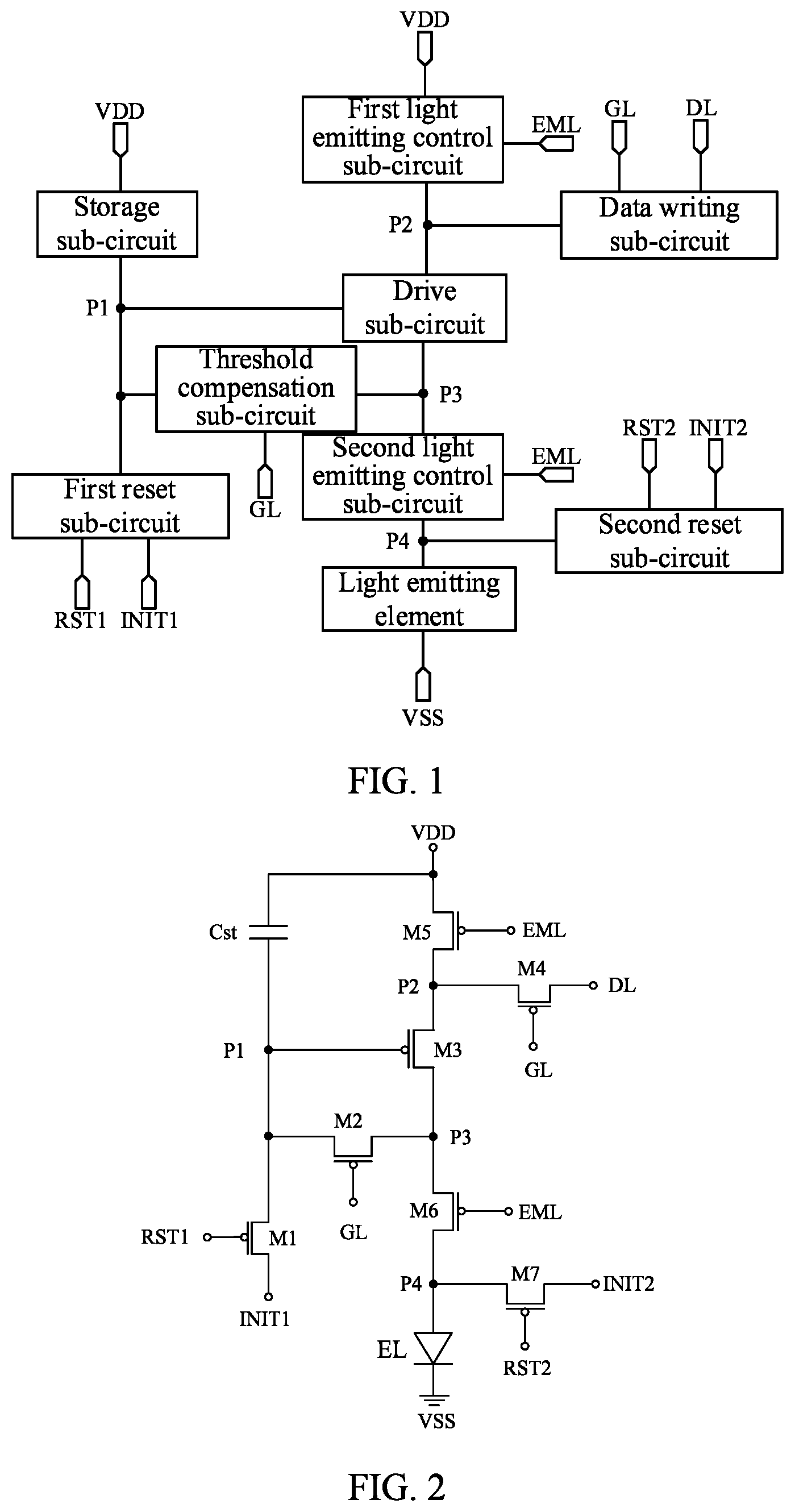
is a schematic diagram of a pixel circuit according to at least one embodiment of the present disclosure. In some exemplary embodiments, as shown in , the pixel circuit of the present embodiment may include a data writing sub-circuit, a drive sub-circuit, a threshold compensation sub-circuit, a storage sub-circuit, a first light emitting control sub-circuit, a second light emitting control sub-circuit, a first reset sub-circuit, and a second reset sub-circuit. The data writing sub-circuit is electrically connected to the scan line GL, the data line DL, and the second pixel node P 2 , and is configured to write the data signal supplied by the data line DL to the second pixel node P 2 under the control of the first scan line GL. The drive sub-circuit is electrically connected to the first pixel node P 1 , the second pixel node P 2 and the third pixel node P 3 , and is configured to provide a drive current to the third pixel node P 3 under the control of the first pixel node P 1 . The first light emitting control sub-circuit is electrically connected to the second pixel node P 2 , the fifth power supply line VDD, and the light emitting control line EML, and is configured to supply a fifth power supply signal transmitted by the fifth power supply line VDD to the second pixel node P 2 under the control of the light emitting control line EML. The second light emitting control sub-circuit, together with the third pixel node P 3 , the fourth pixel node P 4 and the light emitting control line EML, is configured to turn on the third pixel node P 3 and the fourth pixel node P 4 under the control of the light emitting control line EML. The first reset sub-circuit is configured to reset the first pixel node P 1 . The first reset sub-circuit is electrically connected to the first pixel node P 1 , the first reset control line RST 1 , and the first initial signal line INIT 1 , and is configured to supply a first initial signal transmitted by the first initial signal line INIT 1 to the first pixel node P 1 under the control of the first reset control line RST 1 . The second reset sub-circuit is configured to reset the fourth pixel node P 4 . The second reset sub-circuit is electrically connected to the fourth pixel node P 4 , the second reset control line RST 2 , and the second initial signal line INIT 2 , and is configured to supply a second initial signal transmitted by the second initial signal line INIT 2 to the fourth pixel node P 4 under the control of the second reset control line RST 2 . The threshold compensation sub-circuit is electrically connected to the first pixel node P 1 , the third pixel node P 3 and the scan line GL, and is configured to turn on the first pixel node P 1 and the third pixel node P 3 under the control of the scan line GL. The storage sub-circuit is electrically connected to the first pixel node P 1 and the fifth power supply line VDD, and is configured to maintain the potential of the first pixel node P 1 .
is an equivalent circuit diagram of a pixel circuit according to at least one embodiment of the present disclosure. is a working timing diagram of the pixel circuit provided in . The pixel circuit of the present exemplary embodiment is described by taking a 7T1C structure as an example. However, this embodiment is not limited thereto.
In some exemplary embodiments, as shown in , the drive sub-circuit may include a drive transistor M 3 ; the data writing sub-circuit may include a data writing transistor M 4 ; the threshold compensation sub-circuit may include a threshold compensation transistor M 2 ; the first light emitting control sub-circuit may include a first light emitting control transistor M 5 ; the second light emitting control sub-circuit may include a second light emitting control transistor M 6 ; the first reset sub-circuit may include a first reset transistor M 1 ; the second reset sub-circuit may include a second reset transistor M 7 ; and the storage sub-circuit may include a storage capacitor Cst. The light emitting element E 1 may include an anode, a cathode and an organic light emitting layer disposed between the anode and the cathode. In some examples, the organic light-emitting layer may include a multi-layer structure formed by one or more film layers selected from an Emitting Layer (EML), a Hole Injection Layer (HIL), a Hole Transport Layer (HTL), a Hole Block Layer (HBL), an Electron Block Layer (EBL), an Electron Injection Layer (EIL), and an Electron Transport Layer (ETL). For example, under the driving of voltages of the anode and the cathode, the organic light-emitting layer may emit light according to the required gray scale using light emitting properties of the organic materials.
In some exemplary embodiments, the seven transistors of the pixel circuit may be P-type transistors, or may be N-type transistors. Adopting a same type of transistors in a pixel circuit may simplify a process flow, reduce a process difficulty of a display substrate, and improve a yield of products. In some possible embodiments, the seven transistors in the pixel circuit may include P-type transistors and N-type transistors.
In some exemplary embodiments, the seven transistors in the pixel circuit may be low temperature poly-silicon thin film transistors, or may be oxide thin film transistors, or may be low temperature poly-silicon thin film transistors and oxide thin film transistors. An active layer of a Low Temperature Poly-Silicon thin film transistor is made of Low Temperature Poly-Silicon (LTPS), and an active layer of an oxide thin film transistor is made of an oxide semiconductor (Oxide). A Low-temperature Poly-Silicon thin film transistor has advantages such as a high mobility and fast charging, while an oxide thin film transistor has an advantage such as a low leakage current. The Low Temperature Poly-Silicon thin film transistor and the oxide thin film transistor are integrated on one display substrate to form a Low Temperature Polycrystalline Oxide (LTPO) display substrate, and advantages of both the Low Temperature Poly-Silicon thin film transistor and the oxide thin film transistor may be utilized, which may achieve low frequency drive, reduce power consumption, and improve display quality.
In some exemplary embodiments, as shown in , the fifth power supply line VDD is configured to provide a fifth power supply signal of a constant high potential, and the sixth power supply line VSS is configured to provide a sixth power supply signal of a constant low potential. The scan line GL is configured to provide a scan signal SCAN to the pixel circuit, the data line DL is configured to provide a data signal DATA to the pixel circuit, the light emitting control line EML is configured to provide a light emitting control signal EM to the pixel circuit, the first reset control line RST 1 is configured to provide a first reset control signal RESET 1 to the pixel circuit, and the second reset control line RST 2 is configured to provide a second reset control signal RESET 2 to the pixel circuit. In some examples, in a pixel circuit of an n-th row, a first reset control line RST 1 may be electrically connected with a scan line GL of a pixel circuit of an (n−1)-th row to be inputted with a scan signal SCAN(n−1), that is, a first reset control signal RESET 1 ( n ) may be the same as the scan signal SCAN(n−1). Where n is an integer. Thus, signal lines of the display substrate may be reduced, and a narrow bezel of the display substrate may be achieved. However, this embodiment is not limited thereto.
In some exemplary embodiments, the first initial signal line INIT 1 is configured to provide a first initial signal to the pixel circuit, and the second initial signal line INIT 2 is configured to provide a second initial signal to the pixel circuit. The magnitude of the first initial signal and the second initial signal may be the same or different. For example, the first initial signal and the second initial signal may be constant voltage signals whose magnitude may be between the fifth power supply signal and the sixth power supply signal, for example. In some examples, the voltage value of the second initial signal may be less than the voltage value of the first initial signal. For example, the voltage value of the second initial signal may be 2V lower than the voltage value of the first initial signal. However, this embodiment is not limited thereto.
In some exemplary implementations, as shown in , a gate electrode of the data writing transistor M 4 is electrically connected to the scan line GL, a first electrode of the data writing transistor M 4 is electrically connected to the data line DL, and a second electrode of the data writing transistor M 4 is electrically connected to a first electrode of the drive transistor M 3 . A gate of a threshold compensation transistor M 2 is electrically connected with a scan line GL, a first electrode of the threshold compensation transistor M 2 is electrically connected with a gate of the drive transistor M 3 , and a second electrode of the threshold compensation transistor M 2 is electrically connected with a second electrode of the drive transistor M 3 . A gate of a first light emitting control transistor M 5 is electrically connected with an light emitting control line EML, a first electrode of the first light emitting control transistor M 5 is electrically connected with a fifth power supply line VDD, and a second electrode of the first light emitting control transistor M 5 is electrically connected with the first electrode of the drive transistor M 3 . A gate of a second light emitting control transistor M 6 is electrically connected with the light emitting control line EML, a first electrode of the second light emitting control transistor M 6 is electrically connected with the second electrode of the drive transistor M 3 , and a second electrode of the second light emitting control transistor M 6 is electrically connected with an anode of the light emitting element EL. A gate of the first reset transistor M 1 is electrically connected with a first reset control line RST 1 , a first electrode of the first reset transistor M 1 is electrically connected with a first initial signal line INIT 1 , and a second electrode of the first reset transistor M 1 is electrically connected with the gate of the drive transistor M 3 . A gate of the second reset transistor M 7 is electrically connected with a second reset control line RST 2 , a first electrode of the second reset transistor M 7 is electrically connected with a second initial signal line INIT 2 , and a second electrode of the second reset transistor M 7 is electrically connected with the anode of the light emitting element EL. The first electrode plate of the storage capacitor Cst is electrically connected to the gate electrode of the drive transistor M 3 , and the second electrode plate of the storage capacitor Cst is electrically connected to the fifth power supply line VDD. The anode of the light emitting element EL is electrically connected to the fourth pixel node P 4 , and the cathode of the light emitting element EL is electrically connected to the sixth power supply line VSS.
In this example, a first pixel node P 1 is a connection point for the storage capacitor Cst, the first reset transistor M 1 , the drive transistor M 3 , and the threshold compensation transistor M 2 , a second pixel node P 2 is a connection point for the first light emitting control transistor M 5 , the data writing transistor M 4 , and the drive transistor M 3 , a third pixel node P 3 is a connection point for the drive transistor M 3 , the threshold compensation transistor M 2 , and the second light emitting control transistor M 6 , and a fourth pixel node P 4 is a connection point for the second light emitting control transistor M 6 , the second reset transistor M 7 , and the light emitting element EL.
A working process of the pixel circuit shown in will be described below with reference to . The description is given by taking a case in which a plurality of transistors included in the pixel circuit shown in are all P-type transistors as an example.
In some exemplary implementation modes, as shown in , during one frame display period, the working process of the pixel circuit may include a first stage S 11 , a second stage S 12 , a third stage S 13 , and a fourth stage S 14 .
The first stage S 11 is referred to as a first reset stage. The second reset control signal RESET 2 provided by the second reset control line RST 2 is a low-level signal, the second reset transistor M 7 is turned on, and the second initial signal supplied by the second initial signal line INIT 2 is supplied to the fourth pixel node P 4 to reset the anode of the light emitting element EL. The first reset control signal RESET 1 provided by the first reset control line RST 1 is a high-level signal, the scan signal SCAN provided by the scan line GL is a high-level signal, and the light emitting control signal EM provided by the light emitting control line EML is a high-level signal. The first reset transistor M 1 , the data writing transistor M 4 , the threshold compensation transistor M 2 , the first light emitting control transistor M 5 and the second light emitting control transistor M 6 are all turned off. In this stage, the light emitting element EL does not emit light.
The second stage S 12 is referred to as a second reset stage. The first reset control signal RESET 1 provided by the first reset control line RST 1 is a low-level signal, and the first reset transistor M 1 is turned on. The first initial signal provided by the first initial signal line INIT 1 is provided to the first pixel node P 1 to initialize the first pixel node P 1 and clear the original data voltage in the storage capacitor Cst. A scan signal SCAN provided by the scan line GL is a high-level signal, and a light emitting control signal EM provided by the light emitting control line EML is a high-level signal, so that the data writing transistor M 4 , the threshold compensation transistor M 2 , the first light emitting control transistor M 5 , and the second light emitting control transistor M 6 are turned off. The second reset control signal RESET 2 supplied by the second reset control line RST 2 is a low-level signal, and the second reset transistor M 7 is turned on to reset the anode of the light emitting element EL. In this stage, the light emitting element EL does not emit light.
The third stage S 13 is referred to as a data writing stage or a threshold compensation stage. A scan signal SCAN provided by the scan line GL is a low-level signal, a first reset control signal RESET 1 provided by the first reset control line RST 1 and an emitting control signal EM provided by the emitting control line EML are both high-level signals, and the data line DL outputs a data signal DATA. In this phase, the first electrode plate of the storage capacitor Cst is at a low-level, such that the drive transistor M 3 is turned on. The scan signal SCAN is a low-level signal, so that the threshold compensation transistor M 2 , and the data writing transistor M 4 are turned on. The threshold compensation transistor M 2 and the data writing transistor M 4 are turned on, so that the data voltage output by the data line DL is provided to the first pixel node P 1 through the second pixel node P 2 , the turned-on drive transistor M 3 , the third pixel node P 3 , and the turned-on threshold compensation transistor M 2 , and charge the difference between the data voltage output by the data line DL and the threshold voltage of the drive transistor M 3 into the storage capacitor Cst. The voltage of the first electrode plate of the storage capacitor Cst (that is, the first pixel node P 1 ) is Vdata−|Vth|, where Vdata is the data voltage output from the data line DL, and Vth is the threshold voltage of the drive transistor M 3 . The second reset control signal RESET 2 supplied by the second reset control line RST 2 is a low-level signal, and the second reset transistor M 7 is turned on, so that the second initial signal supplied by the second initial signal line INIT 2 is supplied to the anode of the light emitting element EL to ensure that the light emitting element EL does not emit light. The first reset control signal RESET 1 provided by the first reset control line RST 1 is a high-level signal, so that the first reset transistor M 1 is turned off. The light emitting control signal EM provided by the light emitting control signal line EML is a high-level signal, so that the first light emitting control transistor M 5 and the second light emitting control transistor M 6 are turned off.
The fourth stage S 14 is referred to as a light emitting stage. The light emitting control signal EM provided by the light emitting control signal line EML is a low-level signal, so that the first light emitting control transistor M 5 and the second light emitting control transistor M 6 are turned on, and a fifth power supply signal of the high-level output by the fifth power supply line VDD provides a drive voltage to the anode of the light emitting element EL through the turned-on first light emitting control transistor M 5 , the drive transistor M 3 , and the second light emitting control transistor M 6 to drive the light emitting element EL to emit light. The scan signal SCAN supplied by the scan line GL, the first reset control signal RESET 1 supplied by the first reset control line RST 1 , and the second reset control signal RESET 2 supplied by the second reset control line RST 2 are all high-level signals, and the threshold compensation transistor M 2 , the data writing transistor M 4 , the first reset transistor M 1 , and the second reset transistor M 7 are all turned off.
In a drive process of the pixel circuit, a drive current flowing through the drive transistor M 3 is determined by a voltage difference between the gate and the first electrode of the drive transistor T 3 . Because the voltage of the first pixel node P 1 is Vdata−|Vth|, the drive current of the drive transistor M 3 is as follows. I=K ×(Vgs−Vth) 2 =K ×[(Vdd−Vdata+|Vth|)−Vth] 2 =K ×[Vdd−Vdata] 2 .
Among them, I is the drive current flowing through the drive transistor M 3 , that is, the drive current for driving the light emitting element EL; K is a constant; Vgs is the voltage difference between the gate and the first electrode of the drive transistor M 3 ; Vth is the threshold voltage of the drive transistor M 3 ; Vdata is the data voltage output by the data line DL, and Vdd is the fifth power supply signal output from the fifth power supply line VDD.
It may be seen from the above formula that a current flowing through the light emitting element EL has nothing to do with the threshold voltage of the drive transistor M 3 . Therefore, the pixel circuit of this embodiment may better compensate the threshold voltage of the drive transistor M 3 .
In some exemplary embodiments, within the duration of one frame, the overlapping duration between the reset duration of the anode of the light emitting element under the control of the second reset control signal and the duration during which the light emitting element is not driven by the light emitting control signal may be longer than twice the effective level duration of the scan signal supplied by the scan line. For example, the overlapping duration may be approximately three times the effective level duration of the scan signal. The effective level of the scan signal supplied by the scan line may be a low-level.
The present embodiment provides a drive control circuit, which can simultaneously provide a light emitting control signal and a second reset control signal to a pixel circuit in a display region, so that the pixel circuit can control the anode of a light emitting element to be reset by using the second reset control signal, and then control the light emitting element to emit light by using the light emitting control signal. In this example, the reset time of the fourth pixel node under the control of the second reset control signal is longer than the reset time of the first pixel node under the control of the first reset control signal.
In some implementations, the mobility of the hole transport material of the organic small molecule used in the organic light emitting layer of the light emitting element is generally two orders of magnitude higher than that of the electron transport material. Therefore, with the increase of the luminescent duration of the light emitting element, redundant holes will remain, resulting in leakage current and affecting the service life of the light emitting element. The second reset control signal supplied by the embodiment can increase the anode reset time of the light emitting element, so as to maintain the anode reset voltage of the light emitting element for a long time and avoid the formation of leakage current, thereby prolonging the service life of the light emitting element. Moreover, the number of gate drive circuits in the non-display region of the display substrate can be reduced to reduce the area of the circuit of the non-display region, which is beneficial to achieving the narrow bezel design of the display substrate.
is a schematic diagram of a drive control circuit according to at least one embodiment of the present disclosure. In some exemplary implementations, as shown in , the drive control circuit of this embodiment may include: an input circuit 10 , a first output circuit 11 and a second output circuit 12 . The input circuit 10 is electrically connected to a signal input terminal INT, a clock signal terminal (including, for example, a first clock terminal CK and a second clock terminal CB), a first node N 1 and a second node N 2 , and is configured to control the potentials of the first node N 1 and the second node N 2 under the control of the signal input terminal INT and the clock signal terminal. The first output circuit 11 is electrically connected to the first node N 1 , the second node N 2 , the first output terminal OUT 1 , the first power supply line VGH 1 and the second power supply line VGL 1 , and is configured to output a first power supply signal supplied by a first power supply line VGH 1 to a first output terminal OUT 1 under the control of a first node N 1 , or to output a second power supply signal supplied by a second power supply line VGL 1 to a second output terminal OUT 2 under the control of a second node N 2 . The second output circuit 12 is electrically connected to the first node N 1 , the second node N 2 , the second output terminal OUT 2 , the third power supply line VGH 2 and the fourth power supply line VGL 2 , and is configured to output a fourth power supply signal supplied by the fourth power supply line VGL 2 to the second output terminal OUT 2 under the control of the first node N 1 , or to output a third power supply signal supplied by the third power supply line VGH 2 to the second output terminal OUT 2 under the control of the second node N 2 .
In some examples, the first power supply line VGH 1 and the third power supply line VGH 2 may be the same power supply line and the first power supply signal and the third power supply signal may be the same. Alternatively, the first power supply line VGH 1 and the third power supply line VGH 2 may be two different power supply lines, and the first power supply signal supplied by the first power supply line VGH 1 and the third power supply signal supplied by the third power supply line VGH 2 may be the same. Alternatively, the first power supply line VGH 1 and the third power supply line VGH 2 may be two different power supply lines, and the first power supply signal and the third power supply signal may be different. However, this embodiment is not limited thereto.
In some examples, the second power supply line VGL 1 and the fourth power supply line VGL 2 may be the same power supply line, and the second power supply signal and the fourth power supply signal may be the same. Alternatively, the second power supply line VGL 1 and the fourth power supply line VGL 2 may be two different power supply lines, and the second power supply signal supplied by the second power supply line VGL 1 and the fourth power supply signal supplied by the fourth power supply line VGL 2 may be the same. Alternatively, the second power supply line VGL 1 and the fourth power supply line VGL 2 may be two different power supply lines, and the second power supply signal and the fourth power supply signal may be different. However, this embodiment is not limited thereto.
In some examples, the phases of the output signal of the first output terminal OUT 1 and the output signal of the second output terminal OUT 2 may be opposite. However, this embodiment is not limited thereto. For example, the absolute values of the voltages of the effective level of the output signal of the first output terminal OUT 1 and the output signal of the second output terminal OUT 2 may be different.
The drive control circuit provided in this embodiment can provide two kinds of signals (i.e., a light emitting control signal and a second reset control signal) to the pixel circuit. Moreover, the second reset control signal generated by the drive control circuit can maintain the anode reset voltage of the light emitting element for a long time, thus avoiding the formation of leakage current, thereby prolonging the service life of the light emitting element.
is another schematic diagram of a drive control circuit according to at least one embodiment of the present disclosure. In some exemplary embodiments, as shown in , the input circuit 10 may include: an input sub-circuit 100 , a first control sub-circuit 101 , a second control sub-circuit 102 and a third control sub-circuit 103 . The input sub-circuit 100 is electrically connected to the signal input terminal INT, the first clock terminal CK, the second power supply line VGL 1 , the second node N 2 , and the third node N 3 , and is configured to control the potentials of the second node N 2 and the third node N 3 under the control of the first clock terminal CK and the signal input terminal INT. The first control sub-circuit 101 is electrically connected with the second node N 2 , the third node N 3 , the first power supply line VGH 1 , and the second clock terminal CB, and is configured to control the potential of the second node N 2 under the control of the third node N 3 and the second clock terminal CB, or to store the signal supplied by the first power supply line VGH 1 or the second clock terminal CB under the control of the second node N 2 and the third node N 3 . The second control sub-circuit 102 is electrically connected to the first node N 1 , the third node N 3 and the second clock terminal CB, and is configured to control the potential of the first node N 1 under the control of the third node N 3 and the second clock terminal CB. The third control sub-circuit 103 is electrically connected to the first node N 1 , the second node N 2 and the first power supply line VGH 1 , and is configured to control the potential of the first node N 1 under the control of the second node N 2 .
is an equivalent circuit diagram of a drive control circuit according to at least one embodiment of the present disclosure. In some exemplary embodiments, as shown in , the input sub-circuit 100 may include: a third transistor T 3 , a fourth transistor T 4 and a fifth transistor T 5 . The first control sub-circuit 101 may include a first transistor T 1 , a second transistor T 2 , and a third capacitor C 3 . The second control sub-circuit 102 may include: a sixth transistor T 6 , a seventh transistor T 7 and a second capacitor C 2 . The third control sub-circuit 103 may include an eighth transistor T 8 and a first capacitor C 1 . The first output circuit 11 may include a first output transistor T 9 and a second output transistor T 10 . The second output circuit 12 may include a third output transistor T 11 , a fourth output transistor T 12 , and a fourth capacitor C 4 .
In some examples, as shown in , a control electrode of the first transistor T 1 is electrically connected to the third node N 3 , a first electrode of the first transistor T 1 is electrically connected to the first power supply line VGH 1 , and a second electrode of the first transistor T 1 is electrically connected to the first electrode of the second transistor T 2 . A control electrode of the second transistor T 2 is electrically connected to the second clock terminal CB, and a second electrode of the second transistor T 2 is electrically connected to the second node N 2 . A control electrode of the third transistor T 3 is electrically connected to the second node N 2 , a first electrode of the third transistor T 3 is electrically connected to the first clock terminal CK, and a second electrode of the third transistor T 3 is electrically connected to the third node N 3 . A control electrode of the fourth transistor T 4 is electrically connected to the first clock terminal CK, a first electrode of the fourth transistor T 4 is electrically connected to the signal input terminal INT, and a second electrode of the fourth transistor T 4 is electrically connected to the second node N 2 . A control electrode of the fifth transistor T 5 is electrically connected to the first clock terminal CK, a first electrode of the fifth transistor T 5 is electrically connected to the second power supply line VGL 1 , and a second electrode of the fifth transistor T 5 is electrically connected to the third node N 3 . A control electrode of the sixth transistor T 6 is electrically connected to the third node N 3 , a first electrode of the sixth transistor T 6 is electrically connected to the second clock terminal CB, and a second electrode of the sixth transistor T 6 is electrically connected to a first electrode of the seventh transistor T 7 . A control electrode of the seventh transistor T 7 is electrically connected with the second clock terminal CB, and a second electrode of the seventh transistor T 7 is electrically connected with the first node N 1 . A control electrode of the eighth transistor T 8 is electrically connected to the second node N 2 , a first electrode of the eighth transistor T 8 is electrically connected to the first power supply line VGH 1 , and a second electrode of the eighth transistor T 8 is electrically connected to the first node N 1 . A control electrode of the first output transistor T 9 is electrically connected to the first node N 1 , a first electrode is electrically connected to the first power supply line VGH 1 , and a second electrode is electrically connected to the first output terminal OUT 1 . A control electrode of the second output transistor T 10 is electrically connected to the second node N 2 , a first electrode is electrically connected to the second power supply line VGL 1 , and a second electrode is electrically connected to the first output terminal OUT 1 . A control electrode of the third output transistor T 11 is electrically connected to the first node N 1 , a first electrode is electrically connected to the fourth power supply line VGL 2 , and a second electrode is electrically connected to the second output terminal OUT 2 . A control electrode of the fourth output transistor T 12 is electrically connected to the second node N 2 , a first electrode is electrically connected to the third power supply line VGH 2 , and a second electrode is electrically connected to the second output terminal OUT 2 . A first electrode plate of the first capacitor C 1 is electrically connected to the first node N 1 , and a second electrode plate of the first capacitor C 1 is electrically connected to the first power supply line VGH 1 . A first electrode plate of the second capacitor C 2 is electrically connected to the third node N 3 , and a second electrode plate of the second capacitor C 2 is electrically connected to the first electrode of the seventh transistor T 7 . A first electrode plate of the third capacitor C 3 is electrically connected to the second node N 2 , and a second electrode plate of the third capacitor C 3 is electrically connected to the second clock terminal CB. A first electrode plate of the fourth capacitor C 4 is electrically connected to the first node N 1 , and a second electrode plate of the fourth capacitor C 4 is electrically connected to the fourth power supply line VGL 2 .
In this example, the first node N 1 is a connection point of the seventh transistor T 7 , the eighth transistor T 8 , the first output transistor T 9 , the third output transistor T 11 , the first capacitor C 1 , and the fourth capacitor C 4 . The second node N 2 is a connection point of the second transistor T 2 , the third transistor T 3 , the fourth transistor T 4 , the eighth transistor T 8 , the tenth transistor T 10 , the twelfth transistor T 12 and the third capacitor C 3 . The third node N 3 is a connection point of the first transistor T 1 , the third transistor T 3 , the fifth transistor T 5 , the sixth transistor T 6 and the second capacitor C 2 .
In some examples, transistors T 1 to T 12 are of the same type, for example, they are all P-type transistors. However, this embodiment is not limited thereto. For example, a plurality of transistors may all be N-type transistors. In some examples, the P-type transistor may be an LTPS thin film transistor and the N-type transistor may be an oxide thin film transistor such as an IGZO thin film transistor. However, this embodiment is not limited thereto.
In other exemplary embodiments, in , a first voltage stabilizing transistor may be added between the third Node N 3 and the second control sub-circuit 102 , and a second voltage stabilizing transistor may be added between the second node N 2 and the first output circuit 11 and the second output circuit 12 . For example, a control electrode of the first voltage stabilizing transistor may be electrically connected to the second power supply line, a first electrode is electrically connected to the third node, and a second electrode is electrically connected to the gate electrode of the sixth transistor and the first electrode plate of the second capacitor. A control electrode of the second voltage stabilizing transistor may be electrically connected to the second power supply line, a first electrode is electrically connected to the second node, and a second electrode is electrically connected to the first electrode plate of the third capacitor, the control electrode of the second output transistor, and the control electrode of the fourth output transistor. However, this embodiment is not limited thereto. In this example, by adding a voltage stabilizing transistor, the potential of the second node and the third node can be guaranteed to be stable.
is a working sequence diagram of a drive control circuit according to at least one embodiment of the present disclosure. The operation process of the drive control circuit shown in will be described with reference to by taking the operation process of the first-stage drive control circuit as an example. A signal input terminal of the first stage drive control circuit may be electrically connected with the start signal line. The drive control circuit of the present embodiment may include: twelve transistor cells (i.e. transistors T 1 to T 12 ), four capacitor cells (i.e. first capacitor C 1 to fourth capacitor C 4 ), three input terminals (i.e. A first clock terminal CK, a second clock terminal CB and a signal input terminal INT), two output terminals (i.e. a first output terminal OUT 1 and a second output terminal OUT 2 ), and four power supply terminals (i.e. a first power supply line VGH 1 , a second power supply line VGL 1 , a third power supply line VGH 2 and a fourth power supply line VGL 2 ). The first power supply line VGH 1 can continuously provide a high-level first power supply signal, the second power supply line VGL 1 can continuously provide a low-level second power supply signal, the third power supply line VGH 2 can continuously provide a high-level third power supply signal, and the fourth power supply line VGL 2 can continuously provide a low-level fourth power supply signal. For example, the absolute values of the voltages of the effective levels of the first power supply signal, the second power supply signal, the third power supply signal, and the fourth power supply signal may be substantially the same. However, this embodiment is not limited thereto.
As shown in , the working process of the drive control circuit of this example may include the following stages.
The first stage S 21 is referred to as a first shift stage. The signal input terminal INT provides a high-level signal, the first clock terminal CK provides a low-level signal, and the second clock terminal CB provides a high-level signal.
The first clock terminal CK provides a low-level signal, and the fourth transistor T 4 and the fifth transistor T 5 are turned on. The fourth transistor T 4 is turned on, the second node N 2 is at a high potential, and the third transistor T 3 , the eighth transistor T 8 , the second output transistor T 10 and the fourth output transistor T 12 are turned off. The fifth transistor T 5 is turned on, the third node N 3 is at a low potential, and the first transistor T 1 and the sixth transistor T 6 are turned on.
The second clock terminal CB provides a high-level signal, and the second transistor T 2 and the seventh transistor T 7 are turned off. The first node N 1 maintains the high potential of the previous stage, and the first output transistor T 9 and the third output transistor T 11 are turned off. Because both the first output transistor T 9 and the second output transistor T 10 are turned off, the first output terminal OUT 1 maintains the low-level signal before output. Because both the third output transistor T 11 and the fourth output transistor T 12 are turned off, the second output terminal OUT 2 maintains the high-level signal before output.
In the second stage S 22 , it is referred to as an output stage. The signal input terminal INT provides a high-level signal, the first clock terminal CK provides a high-level signal, and the second clock terminal CB provides a low-level signal.
The second clock terminal CB provides a low-level signal, and the second transistor T 2 and the seventh transistor T 7 are turned on. The first clock terminal CK provides a high-level signal, the fourth transistor T 4 and the fifth transistor T 5 are turned off, and the third node N 3 maintains the low potential of the previous stage under the storage function of the second capacitor C 2 . The first transistor T 1 and the sixth transistor T 6 are turned on. The high-level signal supplied by the first power supply line VGH 1 is transmitted to the second node N 2 through the first transistor T 1 and the second transistor T 2 which are turned on, so that the second node N 2 is held at a high potential, so that the third transistor T 3 , the eighth transistor T 8 , the second output transistor T 10 and the fourth output transistor T 12 are all turned off.
A low-level signal supplied by the second clock terminal CB is transmitted to the first node N 1 through a sixth transistor T 6 and a seventh transistor T 7 which are turned on, so that the first node N 1 is at a low potential, and the first output transistor T 9 and the third output transistor T 11 are turned on. The first output terminal OUT 1 outputs a high-level signal supplied by the first power supply line VGH 1 , and the second output terminal OUT 2 outputs a low-level signal supplied by the fourth power supply line VGL 2 .
The third stage S 23 is referred to as a continuous output stage. The signal input terminal INT provides a high-level signal, the first clock terminal CK provides a low-level signal, and the second clock terminal CB provides a high-level signal.
The first clock terminal CK provides a low-level signal, and the fourth transistor T 4 and the fifth transistor T 5 are turned on. The fourth transistor T 4 is turned on, so that the second node N 2 is at a high potential, and the third transistor T 3 , the eighth transistor T 8 , the second output transistor T 10 and the fourth output transistor T 12 are turned off. The fifth transistor T 5 is turned on, so that the third node T 3 is at a low potential, and the first transistor T 1 and the sixth transistor T 6 are turned on. The second clock terminal CB provides a high-level signal, and the second transistor T 2 and the seventh transistor T 7 are turned off. The first node N 1 maintains the low potential of the previous stage, and the first output transistor T 9 and the third output transistor T 11 are turned on. The first output terminal OUT 1 outputs a high-level signal supplied by the first power supply line VGH 1 , and the second output terminal OUT 2 outputs a low-level signal supplied by the fourth power supply line VGL 2 .
The fourth stage S 24 is referred to as a second shift stage. The signal input terminal INT provides a low-level signal, the first clock terminal CK provides a high-level signal, and the second clock terminal CB provides a low-level signal.
The second clock terminal CB provides a low-level signal, and the second transistor T 2 and the seventh transistor T 7 are turned on. The first clock terminal CK provides a high-level signal, and the fourth transistor T 4 and the fifth transistor T 5 are turned off. Under the storage function of the third capacitor C 3 , the second node N 2 maintains the high potential of the previous stage, and the third transistor T 3 , the eighth transistor T 8 , the second output transistor T 10 and the fourth output transistor T 12 are all turned off. Under the storage function of the second capacitor C 2 , the third node N 3 maintains a low potential, and the first transistor T 1 and the sixth transistor T 6 are turned on. A low-level signal supplied by the second clock terminal CB is transmitted to the first node N 1 through a sixth transistor T 6 and a seventh transistor T 7 which are turned on, so that the first node N 1 is at a low potential, and the first output transistor T 9 and the third output transistor T 11 are turned on. The first output terminal OUT 1 outputs a high-level signal supplied by the first power supply line VGH 1 , and the second output terminal OUT 2 outputs a low-level signal supplied by the fourth power supply line VGL 2 .
The fifth stage S 25 is referred to as a pull-down stage. The signal input terminal INT provides a low-level signal, the first clock terminal CK provides a low-level signal, and the second clock terminal CB provides a high-level signal.
The first clock terminal CK provides a low-level signal, and the fourth transistor T 4 and the fifth transistor T 5 are turned on. The second node N 2 is at a low potential, and the third transistor T 3 , the eighth transistor T 8 , the second output transistor T 10 and the fourth output transistor T 12 are all turned on. The third node N 3 is at a low potential, and the first transistor T 1 and the sixth transistor T 6 are turned on. The second clock terminal CB provides a high-level signal, and the second transistor T 2 and the seventh transistor T 7 are turned off. The first node N 1 is at a high potential, and the first output transistor T 9 and the third output transistor T 11 are turned off. The first output terminal OUT 1 outputs a low-level signal supplied by the second power supply line VGL 1 , and the second output terminal OUT 2 outputs a high-level signal supplied by the third power supply line VGH 1 .
The sixth stage S 26 is referred to as a stable stage. The signal input terminal INT provides a low-level signal, the first clock terminal CK provides a high-level signal, and the second clock terminal CB provides a low-level signal.
The first clock terminal CK provides a high-level signal, and the fourth transistor T 4 and the fifth transistor T 5 are turned off. The second node N 2 remain a low potential, and the third transistor T 3 , the eighth transistor T 8 , the second output transistor T 10 and the fourth output transistor T 12 are all turned on. The third node N 3 is at a high potential, and the first transistor T 1 and the sixth transistor T 6 are turned off. The second clock terminal CB provides a low-level signal, and the second transistor T 2 and the seventh transistor T 7 are turned on. The first node N 1 is at a high potential, and the first output transistor T 9 and the third output transistor T 11 are turned off. The first output terminal OUT 1 outputs a low-level signal supplied by the second power supply line VGL 1 , and the second output terminal OUT 2 outputs a high-level signal supplied by the third power supply line VGH 2 .
After the sixth stage S 26 , the fifth stage S 25 and the sixth stage S 26 can be repeated until the signal input terminal INT inputs a high-level signal, and then restart from the first stage S 21 .
According to the working process of the drive control circuit, from the second stage S 22 to the fourth stage S 24 , the first output terminal OUT 1 may output a high-level signal supplied by the first power supply line VGH 1 , and the second output terminal OUT 2 outputs a low-level signal supplied by the fourth power supply line VGL 2 . In other stages, the first output terminal OUT 1 outputs a low-level signal supplied by the second power supply line VGL 1 , and the second output terminal OUT 2 outputs a high-level signal supplied by the third power supply line VGH 2 . For example, the phases of the first output signal supplied by the first output terminal OUT 1 and the second output signal supplied by the second output terminal OUT 2 may be opposite. Taking the example where the effective level of the first output signal is high, and the effective level of the second output signal is low, within a frame duration, the effective level duration of the first output signal and the effective level duration of the second output signal may be approximately the same, and the absolute voltage value of the effective level of the first output signal and the absolute voltage value of the effective level of the second output signal may be approximately the same. Within a frame duration, the overlapping duration of the effective level (for example, high-level) of the first output signal and the effective level (for example, low-level) of the second output signal may be longer than one pulse period of the clock signal. The duty ratio of the first clock signal supplied by the first clock terminal and the second clock signal supplied by the second clock terminal may be the same, and the first clock signal and the second clock signal may be high voltage not at the same time. A duty ratio refers to a proportion of a high-level time length to a whole pulse period within a pulse period (including a high-level time length and a low-level time length). However, this embodiment is not limited thereto. In some examples, due to the presence of the rising edge and the falling edge of the signal, the first output signal may be gradually raised when the second output signal is not completely lowered. However, due to the very small time of the duration, it exceeds the recognition ability of the human eye and will not affect the luminescence of the light emitting element.
In some exemplary embodiments, a first output signal supplied by the first output terminal OUT 1 may be provided to the pixel circuit as a light emitting control signal, and a second output signal supplied by the second output terminal OUT 2 may be provided to the pixel circuit as a second reset control signal. In some examples, the first output signal supplied by the first output terminal of the drive control circuit of the current stage can be transmitted to the signal input terminal of the drive control circuit of the next stage to be as an input signal of the drive control circuit of the next stage. However, this embodiment is not limited thereto.
is another equivalent circuit diagram of a drive control circuit according to at least one embodiment of the present disclosure. In some exemplary embodiments, as shown in , the input sub-circuit 100 may include: a third transistor T 3 , a fourth transistor T 4 and a fifth transistor T 5 . The first control sub-circuit 101 may include a first transistor T 1 ′, a second transistor T 2 ′, and a third capacitor C 3 ′. The second control sub-circuit 102 may include: a sixth transistor T 6 , a seventh transistor T 7 and a second capacitor C 2 . The third control sub-circuit 103 may include an eighth transistor T 8 and a first capacitor C 1 . The first output circuit 11 may include a first output transistor T 9 and a second output transistor T 10 . The second output circuit 12 may include a third output transistor T 11 , a fourth output transistor T 12 , and a fourth capacitor C 4 .
In some examples, as shown in , a control electrode of the first transistor T 1 ′ is electrically connected to the third node N 3 , a first electrode of the first transistor T 1 ′ is electrically connected to the first power supply line VGH 1 , and a second electrode of the first transistor T 1 ′ is electrically connected to the second electrode of the second transistor T 2 ′. A control electrode of the second transistor T 2 ′ is electrically connected with the second node N 2 , and a first electrode of the second transistor T 2 ′ is electrically connected with the second clock terminal CB. A first electrode plate of the third capacitor C 3 ′ is electrically connected to the second node N 2 , and a second electrode plate of the third capacitor C 3 ′ is electrically connected to the second electrode of the second transistor T 2 ′.
The connection relationship between the rest of the transistors and the capacitors of the drive control circuit of the present embodiment can be described as in the previous embodiment and is therefore not described here.
In this example, the first node N 1 is a connection point of the seventh transistor T 7 , the eighth transistor T 8 , the first output transistor T 9 , the third output transistor T 11 , the first capacitor C 1 , and the fourth capacitor C 4 . The second node N 2 is a connection point of the second transistor T 2 ′, the third transistor T 3 , the fourth transistor T 4 , the eighth transistor T 8 , the tenth transistor T 10 , the twelfth transistor T 12 and the third capacitor C 3 ′. The third node N 3 is a connection point of the first transistor T 1 ′, the third transistor T 3 , the fifth transistor T 5 , the sixth transistor T 6 and the second capacitor C 2 .
In other exemplary embodiments, in , a first voltage stabilizing transistor may be disposed between the third Node N 3 and the second control sub-circuit 102 , and a second voltage stabilizing transistor may be disposed between the input sub-circuit 100 and the second node N 2 . For example, a control electrode of the first voltage stabilizing transistor may be electrically connected to the second power supply line, a first electrode is electrically connected to the third node, and a second electrode is electrically connected to the gate electrode of the sixth transistor and the first electrode plate of the second capacitor. A control electrode of the second voltage stabilizing transistor may be electrically connected to the second power supply line, a first electrode is electrically connected to the second electrode of the fourth transistor and the control electrode of the third transistor, and a second electrode is electrically connected to the second node. However, this embodiment is not limited thereto. In this example, by adding a voltage stabilizing transistor, the potential of the second node and the third node can be guaranteed to be stable.
The operation process of the drive control circuit shown in will be described with reference to by taking the operation process of the first-stage drive control circuit as an example. A signal input terminal of the first stage drive control circuit may be electrically connected with the start signal line. The drive control circuit of the present embodiment may include: twelve transistor cells (i.e. transistors T 1 ′ and T 2 ′, and transistors T 3 to T 12 ), four capacitor cells (i.e. first capacitor C 1 , second capacitor C 2 , third capacitor C 3 ′ and fourth capacitor C 4 ), three input terminals (i.e. A first clock terminal CK, a second clock terminal CB and a signal input terminal INT), two output terminals (i.e. a first output terminal OUT 1 and a second output terminal OUT 2 ), and four power supply terminals (i.e. a first power supply line VGH 1 , a second power supply line VGL 1 , a third power supply line VGH 2 and a fourth power supply line VGL 2 ). The first power supply line VGH 1 can continuously provide a high-level first power supply signal, the second power supply line VGL 1 can continuously provide a low-level second power supply signal, the third power supply line VGH 2 can continuously provide a high-level third power supply signal, and the fourth power supply line VGL 2 can continuously provide a low-level fourth power supply signal.
As shown in , the working process of the drive control circuit of this example may include the following stages.
In the first stage S 21 , the first clock terminal CK inputs a low-level signal, the second clock terminal CB inputs a high-level signal, and the signal input terminal INT inputs a high-level signal.
The fourth transistor T 4 and the fifth transistor T 5 are turned on, the second node N 2 is at a high potential, and the third transistor T 3 , the second transistor T 2 ′, the eighth transistor T 8 , the second output transistor T 10 and the fourth output transistor T 12 are turned off. The third node N 3 is at a low potential, and the first transistor T 1 ′ and the sixth transistor T 6 are turned on. The second clock terminal CB inputs a high-level, and the seventh transistor T 7 is turned off. The first node N 1 maintains the high potential of the previous stage, and the first output transistor T 9 and the third output transistor T 11 are turned off. The first output terminal OUT 1 maintains the low-level signal before output, and the second output terminal OUT 2 maintains the high-level signal before output.
In the second stage S 22 , the first clock terminal CK inputs a high-level signal, the second clock terminal CB inputs a low-level signal, and the signal INPUT terminal INPUT inputs a high-level signal.
The fourth transistor T 4 and the fifth transistor T 5 are turned off, the second node N 2 remains at a high potential, and the third transistor T 3 , the second transistor T 2 ′, the eighth transistor T 8 , the second output transistor T 10 and the fourth output transistor T 12 are turned off. The third node N 3 remains at a low potential, and the first transistor T 1 ′ and the sixth transistor T 6 are turned on. The second clock terminal CB inputs a low-level signal, and the seventh transistor T 7 is turned on. The first node N 1 is at a low potential, and the first output transistor T 9 and the third output transistor T 11 are turned on. The first output terminal OUT 1 outputs a high-level signal supplied by the first power supply line VGH 1 , and the second output terminal OUT 2 outputs a low-level signal supplied by the fourth power supply line VGL 2 .
In the third stage S 23 , the first clock terminal CK inputs a low-level signal, the second clock terminal CB inputs a high-level signal, and the signal input terminal INPUT inputs a high-level signal.
The fourth transistor T 4 and the fifth transistor T 5 are turned on, the second node N 2 is at a high potential, and the third transistor T 3 , the second transistor T 2 ′, the eighth transistor T 8 , the second output transistor T 10 and the fourth output transistor T 12 are turned off. The third node N 3 is at a low potential, and the first transistor T 1 ′ and the sixth transistor T 6 are turned on. The second clock terminal CB inputs a high-level signal, and the seventh transistor T 7 is turned off. The first node N 1 remains at a low potential, and the first output transistor T 9 and the third output transistor T 11 are turned on. The first output terminal OUT 1 outputs a high-level signal supplied by the first power supply line VGH 1 , and the second output terminal OUT 2 outputs a low-level signal supplied by the fourth power supply line VGL 2 .
In the fourth stage S 24 , the first clock terminal CK inputs a high-level signal, the second clock terminal CB inputs a low-level signal, and the signal INPUT terminal INPUT inputs a low-level signal.
The fourth transistor T 4 and the fifth transistor T 5 are turned off, the second node N 2 is at a high potential, and the third transistor T 3 , the second transistor T 2 ′, the eighth transistor T 8 , the second output transistor T 10 and the fourth transistor T 12 are turned off. The third node N 3 remains at a low potential, and the first transistor T 1 ′ and the sixth transistor T 6 are turned on. The second clock terminal CB supplies a low-level signal, and the seventh transistor T 7 is turned on. The first node N 1 is at a low potential, and the first output transistor T 9 and the third output transistor T 11 are turned on. The first output terminal OUT 1 outputs a high-level signal supplied by the first power supply line VGH 1 , and the second output terminal OUT 2 outputs a low-level signal supplied by the fourth power supply line VGL 2 .
In the fifth stage S 25 , the first clock terminal CK inputs a low-level signal, the second clock terminal CB inputs a high-level signal, and the signal input terminal INPUT inputs a low-level signal.
The fourth transistor T 4 and the fifth transistor T 5 are turned on, the second node N 2 is at a low potential, and the third transistor T 3 , the second transistor T 2 ′, the eighth transistor T 8 , the second output transistor T 10 and the fourth output transistor T 12 are turned on. The third node N 3 is at a low potential, and the first transistor T 1 ′ and the sixth transistor T 6 are turned on. The second clock terminal CB inputs a high-level signal, and the seventh transistor T 7 is turned off. The first node N 1 is at a high potential, and the first output transistor T 9 and the third output transistor T 11 are turned off. The first output terminal OUT 1 outputs a low-level signal supplied by the second power supply line VGL 1 , and the second output terminal OUT 2 outputs a high-level signal supplied by the third power supply line VGH 2 .
In the sixth stage S 26 , the first clock terminal CK inputs a high-level signal, the second clock terminal CB inputs a low-level signal, and the signal INPUT terminal INPUT inputs a low-level signal.
The fourth transistor T 4 and the fifth transistor T 5 are turned off, the second node N 2 remains at a low potential, and the third transistor T 3 , the second transistor T 2 ′, the eighth transistor T 8 , the second output transistor T 10 and the fourth output transistor T 12 are turned on. The third node N 3 is at a high potential, and the first transistor T 1 ′ and the sixth transistor T 6 are turned off. The second clock terminal CB inputs a low-level signal, and the seventh transistor T 7 is turned on. The first node N 1 is at a high potential, and the first output transistor T 9 and the third output transistor T 11 are turned off. The first output terminal OUT 1 outputs a low-level signal supplied by the second power supply line VGL 1 , and the second output terminal OUT 2 outputs a high-level signal supplied by the third power supply line VGH 2 .
For the rest of the description about the working sequence of the drive control circuit of this embodiment, reference may be made to the description of the foregoing embodiment, so details are not repeated here.
In a drive control circuit provided by the present exemplary embodiment, the first output transistor T 9 and the second output transistor T 10 may be used to control the output of the light emitting control signal, and the third output transistor T 11 and the fourth output transistor T 12 may be used to control the output of the second reset control signal, thereby avoiding the risk of causing excessive output burden of the light emitting control signal or the second reset control signal.
The drive control circuit provided by the present exemplary embodiment supplies a second reset control signal to the pixel circuit. The pixel circuit may use the second reset control signal to write a second initial signal lower than the first initial signal to the anode of the light emitting element, so as to improve the anode reset effect. The second reset control signal of the embodiment can prolong the reset time of the anode of the light emitting element, avoid the formation of leakage current, and prolong the service life of the light emitting element.
is a schematic diagram of a gate drive circuit according to at least one embodiment of the present disclosure. As shown in , the gate drive circuit provided by the present exemplary embodiment may include a plurality of cascaded drive control circuits GOA. A single drive control circuit GOA includes a signal input INT. The structure of the drive control circuit may be as described in the foregoing embodiment, and its realization principle and realization effect are similar, so it will not be described here.
In the present exemplary embodiment, as shown in , a signal input terminal INT of a first stage drive control circuit GOA( 1 ) is connected with a start signal line STV, and a signal input terminal of an i+1 stage drive control circuit GOA(i+1) is electrically connected with a first output terminal of an i stage drive control circuit GOA(i), wherein, i is an integer greater than 0. The first clock terminal CK of the drive control circuit may be electrically connected to the first clock signal line CKL, and the second clock terminal CB may be electrically connected to the second clock signal line CBL.
In the present exemplary embodiment, as shown in , the high-potential power supply line VGH to which each stage drive control circuit is connected may include the first power supply line VGH 1 and the third power supply line VGH 2 , and the low-potential power supply line VGL to which each stage drive control circuit is connected may include the second power supply line VGL 1 and the fourth power supply line VGL 2 . The first power supply line VGH 1 and the third power supply line VGH 2 may be the same line or may be two different lines. The second power supply line VGL 1 and the fourth power supply line VGL 2 may be the same line or may be two different lines. This embodiment is not limited thereto.
is a top view of a drive control circuit according to at least one embodiment of the present disclosure. is a partial cross-sectional schematic diagram taken along a direction P-P′ in . The equivalent circuit of the drive control circuit of this example may be shown in . In the present exemplary embodiment, the first transistor T 1 to the eighth transistor T 8 and the first output transistor T 9 to the fourth output transistor T 12 in the drive control circuit are all P-type transistors and are low-temperature polysilicon thin film transistors. However, this embodiment is not limited thereto. In this example, the first power supply line VGH 1 and the third power supply line VGH 2 supply the same high-level signal, and the second power supply line VGL 1 and the fourth power supply line VGL 2 supply the same low-level signal.
In some exemplary embodiments, as shown in , in a plane parallel to the display substrate, the start signal line STV, the clock signal line, the first power supply line VGH 1 , the drive control circuit, and the second power supply line VGL 1 are arranged in sequence along the first direction X. The start signal line STV, the clock signal line, the first power supply line VGH 1 , and the second power supply line VGL 1 all extend in the second direction Y. The clock signal line may include a first clock signal line CKL and a second clock signal line CBL. The first clock signal line CKL is located on a side of the second clock signal line CBL close to the first power supply line VGH 1 . However, this embodiment is not limited thereto. For example, the first clock signal line may be located on a side of the second clock signal line away from the first power supply line.
In some exemplary embodiments, as shown in , in a plane parallel to the display substrate, the input sub-circuit is adjacent to the first power supply line VGH 1 in the first direction X. The first transistor T 1 and the second transistor T 2 of the first control sub-circuit are adjacent to the first power supply line VGH 1 in the first direction X, and the third capacitor C 3 is located between the input sub-circuit and the first output circuit in the first direction X. The second control sub-circuit is located in the first direction X between the transistor of the first control sub-circuit and the first output circuit. The third control sub-circuit is located between the first output circuit and the second output circuit in the first direction. The second output circuit is adjacent to the second power supply line VGL 1 in the first direction X.
In some exemplary embodiments, as shown in , the fourth transistor T 4 , the fifth transistor T 5 , and the third transistor T 3 of the input sub-circuit are sequentially arranged in a direction away from the first power supply line VGH 1 in the first direction X. The fourth transistor T 4 , the first transistor T 1 and the second transistor T 2 of the first control sub-circuit are sequentially arranged along the second direction Y. The third capacitor C 3 is located between the third transistor T 3 and the second output transistor T 10 in the first direction X. The second capacitor C 2 of the second control sub-circuit is located between the first transistor T 1 and the sixth transistor T 6 in the first direction X. The seventh transistor T 7 is located between the sixth transistor T 6 and the first output transistor T 9 in the first direction X. The eighth transistor T 8 and the first capacitor C 1 of the third control sub-circuit are sequentially arranged along the second direction Y. The second output transistor T 10 and the first output transistor T 9 of the first output circuit are sequentially arranged in the second direction Y. The fourth output transistor T 12 and the third output transistor T 11 of the second output circuit are sequentially arranged in the second direction Y.
In some exemplary embodiments, as shown in , in the direction perpendicular to the display substrate, the non-display region of the display substrate may include: a substrate 30 , and a semiconductor layer 40 , a first conductive layer 41 , a second conductive layer 42 and a third conductive layer 43 disposed on the substrate 30 in sequence. The first insulating layer 31 is disposed between the semiconductor layer 40 and the first conductive layer 41 , the second insulating layer 32 is disposed between the first conductive layer 41 and the second conductive layer 42 , and the third insulating layer 33 is disposed between the second conductive layer 42 and the third conductive layer 43 . In some examples, the first insulating layer 31 to the third insulating layer 33 may be inorganic insulating layers. However, this embodiment is not limited thereto.
A is a top view of the drive control circuit after a semiconductor layer is formed in . As shown in to 12 A , the semiconductor layer 40 in the non-display region at least includes: active layers of a plurality of transistors of the drive control circuit. For example, the semiconductor layer 40 may include an active layer 110 A of the first transistor T 1 to an active layer 180 A of the eighth transistor T 8 , and an active layer of the first output transistor T 9 to an active layer of the fourth output transistor T 12 .
In some examples, a material of the semiconductor layer 40 , for example, may include poly-silicon. An active layer may include at least one channel region and a plurality of doped regions. The channel region may not be doped with an impurity, and has characteristics of a semiconductor. The plurality of doped regions may be on two sides of the channel region and doped with impurities, and thus have conductivity. The impurities may be changed according to the type of the transistor. A doped region of the active layer may be interpreted as a source or a drain of a transistor. For example, a first electrode of the transistor may correspond to the first doped region at a periphery of the channel region of the active layer and doped with impurities, and a second electrode of the transistor may correspond to the second doped region at the periphery of the channel region of the active layer and doped with impurities. In addition, portions of the active layers between the transistors may be interpreted as wirings doped with impurities, and may be used for electrically connecting the transistors.
In some examples, as shown in A , the active layer 110 A of the first transistor T 1 , the active layer 120 A of the second transistor T 2 , the active layer 130 A of the third transistor T 3 , the active layer 140 A of the fourth transistor T 4 , the active layer 150 A of the fifth transistor T 5 , the active layer 160 A of the sixth transistor T 6 , and the active layer 180 A of the eighth transistor T 8 all extend along the second direction Y. The active layer 170 A of the seventh transistor T 7 extends along the first direction X. The active layer 110 A of the first transistor T 1 and the active layer 120 A of the second transistor T 2 may be in an integrated structure such as a strip structure extending in the second direction Y. The active layer 160 A of the sixth transistor T 6 and the active layer 170 A of the seventh transistor T 7 may be in an integrated structure, for example, may be L-shaped.
In some examples, as shown in A , the active layer 110 A of the first transistor T 1 includes: a channel region 110 Aa, and a first doped region 110 Ab and a second doped region 110 Ac located on two sides of the channel region 110 Aa along the second direction Y. The active layer 120 A of the second transistor T 2 includes: a channel region 120 Aa, and a first doped region 120 Ab and a second doped region 120 Ac located on two sides of the channel region 120 Aa along the second direction Y. The first doped region 120 Ab of the active layer 120 A of the second transistor T 2 is connected to the second doped region 110 Ac of the active layer 110 A of the first transistor T 1 . The active layer 130 A of the third transistor T 3 includes: a channel region 130 Aa, and a first doped region 130 Ab and a second doped region 130 Ac located on two sides of the channel region 130 Aa along the second direction Y. The active layer 140 A of the fourth transistor T 4 includes: a channel region 140 Aa, and a first doped region 140 Ab and a second doped region 140 Ac located on two sides of the channel region 140 Aa along the second direction Y. The active layer 150 A of the fifth transistor T 5 includes: a channel region 150 Aa, and a first doped region 150 Ab and a second doped region 150 Ac located on two sides of the channel region 150 Aa along the second direction Y. The active layer 160 A of the sixth transistor T 6 includes: a channel region 160 Aa, and a first doped region 160 Ab and a second doped region 160 Ac located on two sides of the channel region 160 Aa along the second direction Y. The active layer 170 A of the seventh transistor T 7 includes: a channel region 170 Aa, and a first doped region 170 Ab and a second doped region 170 Ac located on two sides of the channel region 170 Aa along the first direction X. The second doped region 160 Ac of the active layer 160 A of the sixth transistor T 6 is connected to the first doped region 170 Ab of the active layer 170 A of the seventh transistor T 7 . The active layer 180 A of the eighth transistor T 8 includes: a channel region 180 Aa, and a first doped region 180 Ab and a second doped region 180 Ac located on two sides of the channel region 180 Aa along the second direction Y.
In some examples, as shown in A , the active layer of the first output transistor T 9 includes a first partition 190 A 1 and a second partition 190 A 2 that are sequentially arranged in the first direction X. The first partition 190 A 1 and the second partition 190 A 2 of the active layer of the first output transistor T 9 each extend in the second direction Y. The first partition 190 A 1 includes channel regions 190 Aa 1 , 190 Aa 2 , and 190 Aa 3 arranged in turn along the second direction Y, a first doped region 190 Ab 1 and a second doped region 190 Ac 1 located on both sides of the channel region 190 Aa 1 along the second direction Y, and a third doped region 190 Ab 2 and a fourth doped region 190 Ac 2 located on both sides of the channel region 190 Aa 3 along the second direction Y. The first doped region 190 Ab 1 and the fourth doped region 190 Ac 2 are located on both sides of the channel region 190 Aa 2 along the second direction Y. The second partition 190 A 2 includes channel regions 190 Aa 4 , 190 Aa 5 , and 190 Aa 6 arranged in turn along the second direction Y, a fifth doped region 190 Ab 3 and a sixth doped region 190 Ac 3 located on both sides of the channel region 190 Aa 4 along the second direction Y, and a seventh doped region 190 Ab 4 and a eighth doped region 190 Ac 4 located on both sides of the channel region 190 Aa 6 along the second direction Y. The fifth doped region 190 Ab 3 and the eighth doped region 190 Ac 4 are located on both sides of the channel region 190 Aa 5 along the second direction Y.
In some examples, as shown in A , the active layer of the second output transistor T 10 includes a first partition 200 A 1 and a second partition 200 A 2 that are sequentially arranged in the first direction X. The first partition 200 A 1 and the second partition 200 A 2 of the active layer of the second output transistor T 10 each extend in the second direction Y. The first partition 200 A 1 includes channel regions 200 Aa 1 , 200 Aa 2 , and 200 Aa 3 arranged in turn along the second direction Y, a first doped region 200 Ab 1 and a second doped region 200 Ac 1 located on both sides of the channel region 200 Aa 1 along the second direction Y, and a third doped region 200 Ab 2 and a fourth doped region 200 Ac 2 located on both sides of the channel region 200 Aa 3 along the second direction Y. The second doped region 200 Ac 1 and the third doped region 200 Ab 2 are located on both sides of the channel region 200 Aa 2 along the second direction Y. The second partition 200 A 2 includes channel regions 200 Aa 4 , 200 Aa 5 , and 200 Aa 6 arranged in turn along the second direction Y, a fifth doped region 200 Ab 3 and a sixth doped region 200 Ac 3 located on both sides of the channel region 200 Aa 4 along the second direction Y, and a seventh doped region 200 Ab 4 and a eighth doped region 200 Ac 4 located on both sides of the channel region 200 Aa 6 along the second direction Y. The sixth doped region 200 Ac 3 and the seventh doped region 200 Ab 4 are located on both sides of the channel region 200 Aa 5 along the second direction Y.
In some examples, as shown in A , the active layer of the third output transistor T 11 includes a first partition 210 A 1 and a second partition 210 A 2 that are sequentially arranged in the first direction X. The first partition 210 A 1 and the second partition 210 A 2 of the active layer of the third output transistor T 11 each extend in the second direction Y. The first partition 210 A 1 includes channel regions 210 Aa 1 , 210 Aa 2 , and 210 Aa 3 arranged in turn along the second direction Y, a first doped region 210 Ab 1 and a second doped region 210 Ac 1 located on both sides of the channel region 210 Aa 1 along the second direction Y, and a third doped region 210 Ab 2 and a fourth doped region 210 Ac 2 located on both sides of the channel region 210 Aa 3 along the second direction Y. The first doped region 210 Ab 1 and the fourth doped region 210 Ac 2 are located on both sides of the channel region 210 Aa 2 along the second direction Y. The second partition 210 A 2 includes channel regions 210 Aa 4 , 210 Aa 5 , and 210 Aa 6 arranged in turn along the second direction Y, a fifth doped region 210 Ab 3 and a sixth doped region 210 Ac 3 located on both sides of the channel region 210 Aa 4 along the second direction Y, and a seventh doped region 210 Ab 4 and a eighth doped region 210 Ac 4 located on both sides of the channel region 210 Aa 6 along the second direction Y. The fifth doped region 210 Ab 3 and the eighth doped region 210 Ac 4 are located on both sides of the channel region 210 Aa 5 along the second direction Y.
In some examples, as shown in A , the active layer of the fourth output transistor T 12 includes a first partition 220 A 1 and a second partition 220 A 2 that are sequentially arranged in the first direction X. The first partition 220 A 1 and the second partition 220 A 2 of the active layer of the fourth output transistor T 12 each extend in the second direction Y. The first partition 220 A 1 includes channel regions 220 Aa 1 , 220 Aa 2 , and 220 Aa 3 arranged in turn along the second direction Y, a first doped region 220 Ab 1 and a second doped region 220 Ac 1 located on both sides of the channel region 220 Aa 1 along the second direction Y, and a third doped region 220 Ab 2 and a fourth doped region 220 Ac 2 located on both sides of the channel region 220 Aa 3 along the second direction Y. The second doped region 220 Ac 1 and the third doped region 220 Ab 2 are located on both sides of the channel region 220 Aa 2 along the second direction Y. The second partition 220 A 2 includes channel regions 220 Aa 4 , 220 Aa 5 , and 220 Aa 6 arranged in turn along the second direction Y, a fifth doped region 220 Ab 3 and a sixth doped region 220 Ac 3 located on both sides of the channel region 220 Aa 4 along the second direction Y, and a seventh doped region 220 Ab 4 and a eighth doped region 220 Ac 4 located on both sides of the channel region 220 Aa 6 along the second direction Y. The sixth doped region 220 Ac 3 and the seventh doped region 220 Ab 4 are located on both sides of the channel region 220 Aa 5 along the second direction Y.
In some examples, as shown in A , the first partition 190 A 1 of the active layer of the first output transistor T 9 and the first partition 200 A 1 of the active layer of the second output transistor T 10 may be in an integrated structure, such as a rectangle. The second partition 190 A 2 of the active layer of the first output transistor T 9 and the second partition 200 A 2 of the active layer of the second output transistor T 10 may are in an integrated structure such as a rectangle. The first partition 210 A 1 of the active layer of the third output transistor T 11 and the first partition 220 A 1 of the active layer of the fourth output transistor T 12 may are in an integrated structure such as a rectangle. The second partition 210 A 2 of the active layer of the third output transistor T 11 and the second partition 220 A 2 of the active layer of the fourth output transistor T 12 may are in an integrated structure such as a rectangle. However, this embodiment is not limited thereto.
B is a top view of the drive control circuit after a first conductive layer is formed in . As shown in to B , the first conductive layer 41 in the non-display region at least includes: control electrodes of a plurality of transistors of the drive control circuit and first electrode plates of a plurality of capacitors. For example, the first conductive layer 41 may include: a control electrode 111 A of the first transistor T 1 , a control electrode 121 A of the second transistor T 2 , control electrodes 131 Aa and 131 Ab of the third transistor T 3 , a control electrode 141 A of the fourth transistor T 4 , a control electrode 151 A of the fifth transistor T 5 , a control electrode 161 A of the sixth transistor T 6 , a control electrode 171 A of the seventh transistor T 7 , a control electrode 181 A of the eighth transistor T 8 , control electrodes 191 Aa, 191 Ab and 191 Ac of the first output transistor T 9 , control electrodes 201 Aa, 201 Ab and 201 Ac of the second output transistor T 10 , control electrodes 211 Aa, 211 Ab and 211 Ac of the third output transistor T 11 , control electrodes 221 Aa, 221 Ab and 221 Ac of the fourth output transistor T 12 , a first electrode plate C 1 - 1 A of the first capacitor C 1 , a first electrode plate C 2 - 1 A of the second capacitor C 2 , a first electrode plate C 3 - 1 A of the third capacitor C 3 , a first electrode plate C 4 - 1 A of the fourth capacitor C 4 , a signal input terminal INT, a first output terminal OUT 1 , a second output terminal OUT 2 , a first connection electrode L 1 and a second connection electrode L 2 . The second output terminal OUT 2 is located in the second direction Y on a side of the first output terminal OUT 1 away from the first output circuit and the second output circuit. The first output terminal OUT 1 and the second output terminal OUT 2 may both extend in the first direction X. The first output terminal OUT 1 of the drive control circuit of this stage can be integrated with the signal input terminal of the drive control circuit of the next stage. However, this embodiment is not limited thereto.
In some examples, as shown in B , the third transistor T 3 may be a double-gate transistor, and the first output transistor T 9 , the second output transistor T 10 , the third output transistor T 11 , and the fourth output transistor T 12 may be a triple-gate transistor to prevent and reduce generation of a leakage current. However, this embodiment is not limited thereto.
In some examples, as shown in B , the control electrode 111 A of the first transistor T 1 , the control electrode 161 A of the sixth transistor T 6 , and the first electrode plate C 2 - 1 A of the second capacitor C 2 may be of an integrated structure. The control electrode 141 A of the fourth transistor T 4 and the control electrode 151 A of the fifth transistor T 5 may be of an integrated structure. The control electrodes 131 Aa and 131 Ab of the third transistor T 3 , the first electrode plate C 3 - 1 A of the third capacitor C 3 , the control electrode 181 A of the eighth transistor T 8 , the control electrodes 201 Aa, 201 Ab and 201 Ac of the second output transistor T 10 , and the control electrodes 221 Aa, 221 Ab and 221 Ac of the fourth output transistor T 12 may be of an integrated structure. The first electrode plate C 1 - 1 A of the first capacitor C 1 , the first electrode plate C 4 - 1 A of the fourth capacitor C 4 , the control electrodes 191 Aa, 191 Ab, and 191 Ac of the first output transistor T 9 , and the control electrodes 211 Aa, 211 Ab, and 211 Ac of the third output transistor T 11 may be of an integrated structure. However, this embodiment is not limited thereto.
C is a top view of the drive control circuit after a second conductive layer is formed in . As shown in to 12 C , the second conductive layer 42 of the non-display region at least includes a second electrode plate that drives a plurality of capacitors of the control circuit. For example, the second conductive layer 42 may include a second electrode plate C 1 - 2 A of the first capacitor C 1 , a second electrode plate C 2 - 2 A of the second capacitor C 2 , a second electrode plate C 3 - 2 A of the third capacitor C 3 , a second electrode plate C 4 - 2 A of the fourth capacitor C 4 , a third connection electrode L 3 , and a fourth connection electrode L 4 . An orthographic projection of the first electrode plate C 1 - 1 A of the first capacitor C 1 on the substrate 30 covers an orthographic projection of the second electrode plate C 1 - 2 A on the substrate 30 . An orthographic projection of the first electrode plate C 2 - 1 A of the second capacitor C 2 on the substrate 30 covers an orthographic projection of the second electrode plate C 2 - 2 A on the substrate 30 . An orthographic projection of the first electrode plate C 3 - 1 A of the third capacitor C 3 on the substrate 30 covers an orthographic projection of the second electrode plate C 3 - 2 A on the substrate 30 . An orthographic projection of the first electrode plate C 4 - 1 A of the fourth capacitor C 4 on the substrate 30 covers an orthographic projection of the second electrode plate C 4 - 2 A on the substrate 30 .
In some examples, as shown in C , the second electrode plate C 1 - 2 A of the first capacitor C 1 and the third connection electrode L 3 may be in an integrated structure. The second electrode plate C 4 - 2 A of the fourth capacitor C 4 and the fourth connection electrode L 4 may be in an integrated structure. However, this embodiment is not limited thereto.
D is a top view of the drive control circuit after a third insulating layer is formed in . As shown in to D , a plurality of via holes is formed on a third insulating layer 33 of the non-display region. The plurality of via holes may include a plurality of first type via holes, a plurality of second type via holes, and a plurality of third type via holes. The third insulating layer 33 , the second insulating layer 32 and the first insulating layer 31 in the first type via holes are removed to expose the surface of the semiconductor layer 40 . The third insulating layer 33 and the second insulating layer 32 in the second type of via holes are removed to expose the surface of the first conductive layer 41 . The third insulating layer 33 inside the third type via holes is removed to expose the surface of the second conductive layer 42 . For example, the first type of via hole may include: a first via hole K 1 to a forty-first via hole K 41 ; the second type of via hole may include a forty-second via hole K 42 to a fifty-ninth via hole K 59 ; and the third type of via hole may include a sixtieth via hole K 60 to a sixty-seventh via hole K 67 .
E is a top view of the drive control circuit after a third conductive layer is formed in . As shown in to 12 E , the third conductive layer 43 of the non-display region may include a plurality of connection electrodes (for example, a fifth connection electrode L 5 to a twenty-fourth connection electrode L 24 ), a first clock signal line CKL, a second clock signal line CBL, a first power supply line VGH 1 , a second power supply line VGL 1 , and a start signal line STV. The start signal line STV, the second clock signal line CBL, the first clock signal line CKL, the first power supply line VGH 1 and the second power supply line VGL 1 all extend along the second direction Y and are arranged in sequence along the first direction X.
In some examples, as shown in to 12 E , the fifth connection electrode L 5 may be electrically connected to the first doped region 140 Ab of the active layer 140 A of the fourth transistor T 4 through the first via hole K 1 , and may be electrically connected to the signal input terminal INT through the forty-second via hole K 42 . The sixth connection electrode L 6 may be electrically connected to the second doped region 140 Ac of the active layer 140 A of the fourth transistor T 4 through the second via hole K 2 , may be electrically connected to the second doped region 120 Ac of the active layer 120 A of the second transistor T 2 through the third via hole K 3 , and may be electrically connected to the control electrode 131 Aa of the third transistor T 3 through the forty-sixth via hole K 46 . The first power supply line VGH 1 may be electrically connected to the first doped region 110 Ab of the active layer 110 A of the first transistor T 1 through the fourth via hole K 4 . The seventh connection electrode L 7 may be electrically connected to the second doped region 150 Ac of the active layer 150 A of the fifth transistor T 5 through the sixth via hole K 6 , may be electrically connected to the second doped region 130 Ac of the active layer 130 A of the third transistor T 3 through the eighth via hole K 8 , and may be electrically connected to the control electrode 161 A of the sixth transistor T 6 through the forty-eighth via hole K 48 . An orthographic projection of the seventh connection electrode L 7 on the substrate may be L-shaped. The eighth connection electrode L 8 may be electrically connected to the second doped region 160 Ac of the active layer 160 A of the sixth transistor T 6 through a tenth via hole K 10 , and may be electrically connected to the second electrode plate C 2 - 2 A of the second capacitor C 2 through two sixty-first via hole K 61 arranged vertically. An orthographic projection of the eighth connection electrode L 8 on the substrate may be T-shaped. The ninth connection electrode L 9 may be electrically connected to the second doped region 170 Ac of the active layer 170 A of the seventh transistor T 7 through the eleventh via hole K 11 , and may be electrically connected to the control electrode 191 Ac of the first output transistor T 9 through the fiftieth via hole K 50 . The tenth connection electrode L 10 may be electrically connected to the first doped region 130 Ab of the active layer 130 A of the third transistor T 3 through a seventh via hole K 7 , and may be electrically connected to the control electrode 151 A of the fifth transistor T 5 through a forty-third via hole K 43 . The first clock signal line CKL may be electrically connected to the control electrode 151 A of the fifth transistor T 5 through two forty-fourth via holes K 44 arranged vertically. The eleventh connection electrode L 11 may be electrically connected to the second electrode plate C 3 - 2 A of the third capacitor C 3 through four sixtieth via holes K 60 arranged vertically. It may be electrically connected to the first doped region 160 Ab of the active layer 160 A of the sixth transistor T 6 through the ninth via hole K 9 , may be electrically connected to the control electrode 171 A of the seventh transistor T 7 through the forty-ninth via hole K 49 , and may be electrically connected to the control electrode 121 A of the second transistor T 2 through the forty-seventh via hole K 47 . An orthographic projection of the eleventh connection electrode L 11 on the substrate may be L-shaped. The second clock signal line CBL may be electrically connected to the control electrode 121 A of the second transistor T 2 through two forty-fifth via holes K 45 arranged vertically.
In some examples, the twelfth connection electrode L 12 may be electrically connected to the first doped region 150 Ab of the active layer 150 A of the fifth transistor T 5 through the fifth via hole K 5 , may be electrically connected to the first doped region 200 Ab 1 of the first partition 200 A 1 of the active layer of the second output transistor T 10 through a plurality (e.g. three) of the twelfth via hole K 12 arranged side by side, may be electrically connected to the fifth doped region 200 Ab 3 of the second partition 200 A 2 of the active layer of the second output transistor T 10 through a plurality (e.g. three) of the thirteenth via hole K 13 arranged side by side, may be electrically connected to the third doped region 200 Ab 2 of the first partition 200 A 1 of the active layer of the second output transistor T 10 through a plurality (e.g. three) of the sixteenth via holes K 16 arranged side by side, and may be electrically connected to the seventh doped region 200 Ab 4 of the second partition 200 A 2 of the active layer of the second output transistor T 10 through a plurality (e.g. three) of the seventeenth via hole K 17 arranged side by side. The twelfth connection electrode L 12 and the second power supply line VGL 1 may be of an integrated structure.
In some examples, the thirteenth connection electrode L 13 may be electrically connected to the second doped region 200 Ac 1 of the first partition 200 A 1 of the active layer of the second output transistor T 10 through a plurality (e.g. three) of the fourteenth via hole K 14 arranged side by side, may be electrically connected to the sixth doped region 200 Ac 3 of the second partition 200 A 2 of the active layer of the second output transistor T 10 through a plurality (e.g. three) of the fifteenth via hole K 15 arranged side by side, may be electrically connected to the fourth doped region 200 Ac 2 of the first partition 200 A 1 of the active layer of the second output transistor T 10 through a plurality (e.g. three) of the eighteenth via hole K 18 arranged side by side, may be electrically connected to the eighth doped region 200 Ac 4 of the second partition 200 A 2 of the active layer of the second output transistor T 10 through a plurality (e.g. three) of the nineteenth via hole K 19 arranged side by side, may be electrically connected to the second doped region 190 Ac 1 of the first partition 190 A 1 of the active layer of the first output transistor T 9 through a plurality (e.g. three) of the twenty-second via hole K 22 arranged side by side, may be electrically connected to the eighth doped region 190 Ac 4 of the second partition 190 A 2 of the active layer of the first output transistor T 9 through a plurality (e.g. three) of the twenty-third via hole K 23 arranged side by side, and may be electrically connected to the first output terminal OUT 1 through two fifty-sixth via holes K 56 arranged side by side.
In some examples, the fourteenth connection electrode L 14 may be electrically connected to the first doped region 190 Ab 1 of a first partition 190 A 1 of the active layer of the first output transistor T 9 through a plurality (e.g. three) of the twentieth via hole K 20 arranged side by side, may be electrically connected to the fifth doped region 190 Ab 3 of the second partition 190 A 2 of the active layer of the first output transistor T 9 through a plurality (e.g. three) of the twenty-first via hole K 21 arranged side by side, and may be electrically connected to the second electrode plate C 1 - 2 A of the first capacitor C 1 through the sixty-second via hole K 62 .
In some examples, the fifteenth connection electrode L 15 may be electrically connected to the third doped region 190 Ab 2 of a first partition 190 A 1 of the active layer of the first output transistor T 9 through a plurality (e.g. three) of the twenty-fourth via hole K 24 arranged side by side, may be electrically connected to the seventh doped region 190 Ab 4 of the second partition 190 A 2 of the active layer of the first output transistor T 9 through a plurality (e.g. three) of the twenty-fifth via hole K 25 arranged side by side, and may be electrically connected to the second electrode plate C 1 - 2 A of the first capacitor C 1 through the sixty-third via hole K 63 .
In some examples, the sixteenth connection electrode L 16 may be electrically connected to the first doped region 180 Ab of the active layer 180 A of the eighth transistor T 8 through the twenty-sixth via hole K 26 , and may be electrically connected to the second connection electrode L 2 through the fifty-first via hole K 51 . The second connection electrode L 2 may be electrically connected to the twenty-second connection electrode L 22 through the fifty-third via hole K 53 . The seventeenth connection electrode L 17 may be electrically connected to the second doped region 180 Ac of the active layer 180 A of the eighth transistor T 8 through the twenty-seventh via hole K 27 , and may be electrically connected to the first electrode plate C 1 - 1 A of the first capacitor C 1 through the fifty-second via hole K 52 .
In some examples, the eighteenth connection electrode L 18 may be electrically connected to the first doped region 220 Ab 1 of a first partition 220 A 1 of the active layer of the fourth output transistor T 12 through a plurality (e.g. three) of the twenty-eighth via hole K 28 arranged side by side, may be electrically connected to the fifth doped region 220 Ab 3 of the second partition 220 A 2 of the active layer of the fourth output transistor T 12 through a plurality (e.g. three) of the twenty-ninth via hole K 29 arranged side by side, may be electrically connected to the third doped region 220 Ab 2 of the first partition 220 A 1 of the active layer of the fourth output transistor T 12 through a plurality (e.g. three) of the thirty-second via hole K 32 arranged side by side, may be electrically connected to the seventh doped region 220 Ab 4 of the second partition 220 A 2 of the active layer of the fourth output transistor T 12 through a plurality (e.g. three) of the thirty-third via hole K 33 arranged side by side, and may be electrically connected to the first connection electrode L 1 through two fifty-fourth via holes K 54 arranged side by side. The first connection electrode L 1 may be electrically connected to the twenty-third connection electrode L 23 through two fifty-fifth via holes K 55 arranged vertically.
In some examples, the nineteenth connection electrode L 19 may be electrically connected to the first doped region 210 Ab 1 of a first partition 210 A 1 of the active layer of the third output transistor T 11 through a plurality (e.g. three) of the thirty-sixth via hole K 36 arranged side by side, may be electrically connected to the fifth doped region 210 Ab 3 of the second partition 210 A 2 of the active layer of the third output transistor T 11 through a plurality (e.g. three) of the thirty-seventh via hole K 37 arranged side by side, and may be electrically connected to the second electrode plate C 4 - 2 A of the fourth capacitor C 4 through the sixty-fourth via hole K 64 .
In some examples, the twentieth connection electrode L 20 may be electrically connected to the second doped region 220 Ac 1 of a first partition 220 A 1 of the active layer of the fourth output transistor T 12 through a plurality (e.g. three) of the thirtieth via hole K 30 arranged side by side, may be electrically connected to the sixth doped region 220 Ac 3 of the second partition 220 A 2 of the active layer of the fourth output transistor T 12 through a plurality (e.g. three) of the thirty-first via hole K 31 arranged side by side, may be electrically connected to the fourth doped region 220 Ac 2 of the first partition 220 A 1 of the active layer of the fourth output transistor T 12 through a plurality (e.g. three) of the thirty-fourth via hole K 34 arranged side by side, may be electrically connected to the eighth doped region 220 Ac 4 of the second partition 220 A 2 of the active layer of the fourth output transistor T 12 through a plurality (e.g. three) of the thirty-fifth via hole K 35 arranged side by side, may be electrically connected to the fourth doped region 210 Ac 2 of the first partition 210 A 1 of the active layer of the third output transistor T 11 through a plurality (e.g. three) of the thirty-eighth via hole K 38 arranged side by side, may be electrically connected to the eighth doped region 210 Ac 4 of the second partition 210 A 2 of the active layer of the third output transistor T 11 through a plurality (e.g. three) of the thirty-ninth via hole K 39 arranged side by side, and may be electrically connected to the second output terminal OUT 2 through two fifty-eighth via holes K 58 arranged side by side.
In some examples, the twenty-first connection electrode L 21 may be electrically connected to the third doped region 210 Ab 2 of the first partition 210 A 1 of the active layer of the third output transistor T 11 through a plurality (e.g. three) of the fortieth via hole K 40 arranged side by side, may be electrically connected to the seventh doped region 210 Ab 4 of the second partition 210 A 2 of the active layer of the third output transistor T 11 through a plurality (e.g. three) of the forty-first via hole K 41 arranged side by side, and may be electrically connected to the second electrode plate C 4 - 2 A of the fourth capacitor C 4 through the sixty-fifth via hole K 65 .
In some examples, the third connection electrode L 3 may be electrically connected to the twenty-fourth connection electrode L 24 through two sixty-seventh via holes K 67 arranged vertically. The twenty-second connection electrode L 22 , the twenty-third connection electrode L 23 , and the twenty-fourth connection electrode L 24 may be electrically connected to a third power supply line near the display region side, for example, may be integrated with the third power supply line. The third power supply line may be configured to provide a high-level power supply signal to an adjacent gate drive circuit. However, this embodiment is not limited thereto.
In some examples, the twenty-fifth connection electrode L 25 may be electrically connected to the first output terminal OUT 1 through two fifty-seventh via holes K 57 arranged side by side. The twenty-sixth connection electrode L 26 may be electrically connected to the second output terminal OUT 2 through two fifty-ninth via holes K 59 arranged side by side. The twenty-fifth connection electrode L 25 and the twenty-sixth connection electrode L 26 may extend in the first direction X. For example, the twenty-fifth connection electrode L 25 may be electrically connected to the light emitting control line to supply the light emitting control signal to the pixel circuit of the display region, and the twenty-sixth connection electrode L 26 may be electrically connected to the second reset control line to supply the second reset control signal to the pixel circuit of the display region. However, this embodiment is not limited thereto.
In some examples, the second power supply line VGL 1 may be electrically connected to the fourth connection electrode L 4 through two sixty-sixth via holes K 66 arranged vertically.
In the embodiments of the present disclosure, “disposed side by side” may mean being disposed in sequence along the first direction X, and “disposed vertically” may mean being disposed in sequence along the second direction Y.
In the present exemplary embodiment, electrical connection with the first clock signal line CKL is achieved through the control electrodes of the fourth transistor and the fifth transistor. The electrical connection to the second clock signal line CBL is achieved through a control electrode of the second transistor and an eleventh connection electrode L 11 . The electrical connection between the second power supply line VGL 1 and the second output circuit is achieved through the fourth connection electrode L 4 . The transmission of a second power supply signal to the first output circuit is achieved through a third connection electrode L 3 and a twenty-fourth connection electrode L 24 . The electrical connection between the first output circuit, the input circuit, and the first power supply line is achieved through the twelfth connection electrode L 12 . The transmission of the first power signal to the second output circuit is achieved through the twenty-third connection electrode L 23 and the first connection electrode L 1 .
In the display substrate provided by the exemplary embodiment, a light emitting control signal and a second reset control signal are provided to a pixel circuit by a drive control circuit, thereby saving arrangement space and achieving a display substrate with a narrow bezel design.
is another top view of the drive control circuit according to at least one embodiment of the present disclosure. is a partial cross-sectional schematic diagram along a Q-Q′ direction in . The equivalent circuit of the drive control circuit of this example may be shown in . In the present exemplary embodiment, the first transistor T 1 ′, the second transistor T 2 ′, the third transistor T 3 to the eighth transistor T 8 and the first output transistor T 9 to the fourth output transistor T 12 in the drive control circuit are all P-type transistors and are low-temperature polysilicon thin film transistors. However, this embodiment is not limited thereto. In this example, the first power supply line VGH 1 and the third power supply line VGH 2 supply the same high-level signal, and the second power supply line VGL 1 and the fourth power supply line VGL 2 supply the same low-level signal.
In some exemplary embodiments, as shown in , in a plane parallel to the display substrate, the start signal line STV, the clock signal line, the second power supply line VGL 1 , the drive control circuit, and the first power supply line VGH 1 are arranged in sequence along the first direction X. The start signal line STV, the clock signal line, the first power supply line VGH 1 , and the second power supply line VGL 1 all extend in the second direction Y. The clock signal line may include a first clock signal line CKL and a second clock signal line CBL. The first clock signal line CKL is located on a side of the second clock signal line CBL close to the second power supply line VGL 1 . However, this embodiment is not limited thereto. For example, the first clock signal line may be located on a side of the second clock signal line away from the first power supply line.
In some exemplary embodiments, as shown in , in a plane parallel to the display substrate, the input sub-circuit is adjacent to the second power supply line VGL 1 in the first direction X. The third capacitor C 3 ′, the second transistor T 2 ′, and the first transistor T 1 ′ of the first control sub-circuit are arranged in the second direction Y. The second transistor T 2 ′ and the third capacitor C 3 ′ are located between the input sub-circuit and the first output circuit in the first direction X. A second capacitor C 2 of the second control sub-circuit is adjacent to the second power supply line VGL 1 . The first transistor T 1 ′ is located between the sixth transistor T 6 and the seventh transistor T 7 in the first direction X. The third control sub-circuit is located on a side of the first output circuit close to the second control sub-circuit. The second output circuit is located between the first output circuit and the first power supply line VGH 1 in the first direction X.
In some exemplary embodiments, as shown in , the fourth transistor T 4 , the third transistor T 3 , and the fifth transistor T 5 of the input sub-circuit are sequentially arranged in a direction away from the second power supply line VGL 1 in the first direction X. The second capacitor C 2 , the sixth transistor T 6 , the first transistor T 1 ′, the seventh transistor T 7 , the eighth transistor T 8 , and the first capacitor C 1 are sequentially arranged in a direction away from the second power supply line VGL 1 in the first direction X. The third capacitor C 3 ′ and the second transistor T 2 ′ are sequentially arranged in the second direction Y and are located between the fifth transistor T 5 and the second output transistor T 10 in the first direction X. The second output transistor T 10 and the first output transistor T 9 are sequentially arranged in the second direction Y, and the fourth output transistor T 12 and the third output transistor T 11 are sequentially arranged in the second direction Y. The fourth capacitor C 4 is located between the first output transistor T 9 and the third output transistor T 11 in the first direction X.
In some exemplary embodiments, as shown in , in the direction perpendicular to the display substrate, the non-display region of the display substrate may include: a substrate 30 , and a semiconductor layer 40 , a first conductive layer 41 , a second conductive layer 42 and a third conductive layer 43 disposed on the substrate 30 in sequence. The first insulating layer 31 is disposed between the semiconductor layer 40 and the first conductive layer 41 , the second insulating layer 32 is disposed between the first conductive layer 41 and the second conductive layer 42 , and the third insulating layer 33 is disposed between the second conductive layer 42 and the third conductive layer 43 . In some examples, the first insulating layer 31 to the third insulating layer 33 may be inorganic insulating layers. However, this embodiment is not limited thereto.
A is a top view of the drive control circuit after a semiconductor layer is formed in . As shown in to 15 , the semiconductor layer 40 in the non-display region at least includes: active layers of a plurality of transistors of the drive control circuit. For example, the semiconductor layer 40 may include an active layer 110 B of the first transistor T 1 ′ to an active layer 180 B of the eighth transistor T 8 , an active layer 190 B of the first output transistor T 9 to an active layer 220 B of the fourth output transistor T 12 .
In some examples, as shown in A , the active layer 110 B of the first transistor T 1 ′, the active layer 140 B of the fourth transistor T 4 , the active layer 150 B of the fifth transistor T 5 , the active layer 160 B of the sixth transistor T 6 , and the active layer 180 B of the eighth transistor T 8 all extend in the second direction Y, the active layer 120 B of the second transistor T 2 ′ extends in the first direction X, and the active layer 130 B of the third transistor T 3 is U-shaped. The active layer 190 B of the first output transistor T 9 , the active layer 200 B of the second output transistor T 10 , the active layer 210 B of the third output transistor T 11 , and the active layer 220 B of the fourth output transistor T 12 are all rectangular.
In some examples, as shown in A , the active layer 110 B of the first transistor T 1 ′ includes: a channel region 110 Ba, and a first doped region 110 Bb and a second doped region 110 Bc located on both sides of the channel region 110 Ba along the second direction Y. The active layer 120 B of the second transistor T 2 ′ includes: a channel region 120 Ba, and a first doped region 120 Bb and a second doped region 120 Bc located on both sides of the channel region 120 Ba along the first direction X. The active layer 130 B of the third transistor T 3 includes: a channel region 130 Ba, and a first doped region 130 Bb and a second doped region 130 Bc located at two sides of the channel region 130 Ba. The active layer 140 B of the fourth transistor T 4 includes: a channel region 140 Ba, and a first doped region 140 Bb and a second doped region 140 Bc located on two sides of the channel region 140 Ba along the second direction Y. The active layer 150 B of the fifth transistor T 5 includes: a channel region 150 Ba, and a first doped region 150 Bb and a second doped region 150 Bc located on two sides of the channel region 150 Ba along the second direction Y. The active layer 160 B of the sixth transistor T 6 includes: a channel region 160 Ba, and a first doped region 160 Bb and a second doped region 160 Bc located on two sides of the channel region 160 Ba along the second direction Y. The active layer 170 b of the seventh transistor T 7 includes: a channel region 170 Ba, and a first doped region 170 Bb and a second doped region 170 Bc located on two sides of the channel region 170 Aa along the first direction X. The active layer 180 B of the eighth transistor T 8 includes: a channel region 180 Ba, and a first doped region 180 Bb and a second doped region 180 Bc located on two sides of the channel region 180 Ba along the second direction Y.
In some examples, the active layer 190 B of the first output transistor T 9 includes channel regions 190 Ba 1 , 190 Ba 2 , 190 Ba 3 , and 190 Ba 4 arranged in sequence along the first direction X, a first doped region 190 Bb 1 and a second doped region 190 Bc 1 on both sides of the channel region 190 Ba 1 along the first direction X, a third doped region 190 Bb 2 and a fourth doped region 190 Bc 2 on both sides of the channel region 190 Ba 4 along the first direction X, and a fifth doped region 190 Bc 3 between the channel regions 190 Ba 2 and 190 Ba 3 . The third doped region 190 Bb 2 is located between channel regions 190 Ba 3 and 190 Ba 4 , and the first doped region 190 Bb 1 is located between channel regions 190 Ba 1 and 190 Ba 2 .
In some examples, the active layer 200 B of the second output transistor T 10 includes channel regions 200 Ba 1 , 200 Ba 2 , 200 Ba 3 , and 200 Ba 4 arranged in sequence along the first direction X, a first doped region 200 Bb 1 and a second doped region 200 Bc 1 on both sides of the channel region 200 Ba 1 along the first direction X, a third doped region 200 Bb 2 and a fourth doped region 200 Bc 2 on both sides of the channel region 200 Ba 4 along the first direction X, and a fifth doped region 200 Bc 3 between the channel regions 200 Ba 2 and 200 Ba 3 . The third doped region 200 Bb 2 is located between channel regions 200 Ba 3 and 200 Ba 4 , and the first doped region 200 Bb 1 is located between channel regions 200 Ba 1 and 200 Ba 2 .
In some examples, the active layer 210 B of the third output transistor T 11 includes channel regions 210 Ba 1 , 210 Ba 2 , 210 Ba 3 , and 210 Ba 4 arranged in sequence along the first direction X, a first doped region 210 Bb 1 and a second doped region 210 Bc 1 on both sides of the channel region 210 Ba 1 along the first direction X, a third doped region 210 Bb 2 and a fourth doped region 210 Bc 2 on both sides of the channel region 210 Ba 4 along the first direction X, and a fifth doped region 210 Bc 3 between the channel regions 210 Ba 2 and 210 Ba 3 . The third doped region 210 Bb 2 is located between channel regions 210 Ba 3 and 210 Ba 4 , and the first doped region 210 Bb 1 is located between channel regions 210 Ba 1 and 210 Ba 2 .
In some examples, the active layer 220 B of the fourth output transistor T 12 includes channel regions 220 Ba 1 , 220 Ba 2 , 220 Ba 3 , and 220 Ba 4 arranged in sequence along the first direction X, a first doped region 220 Bb 1 and a second doped region 220 Bc 1 on both sides of the channel region 220 Ba 1 along the first direction X, a third doped region 220 Bb 2 and a fourth doped region 220 Bc 2 on both sides of the channel region 220 Ba 4 along the first direction X, and a fifth doped region 220 Bc 3 between the channel regions 220 Ba 2 and 220 Ba 3 . The third doped region 220 Bb 2 is located between channel regions 220 Ba 3 and 220 Ba 4 , and the first doped region 220 Bb 1 is located between channel regions 220 Ba 1 and 220 Ba 2 .
In some examples, as shown in A , the active layer 130 B of the third transistor T 3 and the active layer 150 B of the fifth transistor T 5 may be of an integrated structure. The active layer 110 B of the first transistor T 1 ′, the active layer 180 B of the eighth transistor T 8 , and the active layer 170 B of the seventh transistor T 7 may be of an integrated structure. However, this embodiment is not limited thereto.
B is a top view of the drive control circuit after a first conductive layer is formed in . As shown in to B , the first conductive layer 41 in the non-display region at least includes: control electrodes of a plurality of transistors of the drive control circuit and first electrode plates of a plurality of capacitors. For example, the first conductive layer 41 may include: a control electrode 111 B of the first transistor T 1 ′, a control electrode 121 B of the second transistor T 2 ′, a control electrode 131 B of the third transistor T 3 , a control electrode 141 B of the fourth transistor T 4 , a control electrode 151 B of the fifth transistor T 5 , a control electrode 161 B of the sixth transistor T 6 , a control electrode 171 B of the seventh transistor T 7 , a control electrode 181 B of the eighth transistor T 8 , control electrodes 191 Ba, 191 Bb, 191 Bc and 191 Bd of the first output transistor T 9 , control electrodes 201 Ba, 201 Bb, 201 Bc and 201 Bd of the second output transistor T 10 , control electrodes 211 Ba, 211 Bb, 211 Bc and 211 Bd of the third output transistor T 11 , control electrodes 221 Ba, 221 Bb, 221 Bc and 221 Bd of the fourth output transistor T 12 , a first electrode plate C 1 - 1 B of the first capacitor C 1 , a first electrode plate C 2 - 1 B of the second capacitor C 2 , a first electrode plate C 3 - 1 B of the third capacitor C 3 ′, a first electrode plate C 4 - 1 B of the fourth capacitor C 4 , a first output terminal OUT 1 , a second output terminal OUT 2 , and a plurality of connection electrodes (e.g. thirty-first connection electrode L 31 to thirty-fourth connection electrode L 34 ).
In some examples, the first output OUT 1 includes a first portion 301 extending in a second direction Y, a second portion 302 and a third portion 303 extending in a first direction X. The first portion 301 of the first output OUT 1 is located between the first output circuit and the second output circuit. The second portion 302 and the third portion 303 are located on the same side of the first output circuit and the second output circuit in the second direction Y. The second output terminal OUT 2 includes a fourth portion 304 extending in the second direction Y and a fifth portion 305 extending in the first direction X. An orthographic projection of the second output terminal OUT 2 on the substrate may be L-shaped. The fifth portion 305 is located on a side of the third portion 303 close to the second output circuit.
The first output terminal OUT 1 of the current stage drive control circuit can be electrically connected with the signal input terminal of the next stage drive control circuit. However, this embodiment is not limited thereto.
In some examples, as shown in B , the first output transistor T 9 , the second output transistor T 10 , the third output transistor T 11 , and the fourth output transistor T 12 may be a quad-gate transistor to prevent and reduce generation of a leakage current. However, this embodiment is not limited thereto.
In some examples, as shown in B , the control electrode 141 B of the fourth transistor T 4 and the control electrode 151 B of the fifth transistor T 5 may be in an integrated structure. The control electrode 131 B of the third transistor T 3 and the control electrode 181 B of the eighth transistor T 8 may be in an integrated structure. The control electrode 161 B of the sixth transistor T 6 and the first electrode plate C 2 - 1 B of the second capacitor C 2 may be in an integrated structure. The first electrode plate C 1 - 1 B of the first capacitor C 1 and the control electrodes 191 Ba, 191 Bb, 191 Bc and 191 Bd of the first output transistor T 9 may be in an integrated structure. The control electrode 121 B of the second transistor T 2 ′, the first electrode plate C 3 - 1 B of the third capacitor C 3 ′, the control electrodes 201 Ba, 201 Bb, 201 Bc and 201 Bd of the second output transistor T 10 , and the control electrodes 221 Ba, 221 Bb, 221 Bc and 221 Bd of the fourth output transistor T 12 may be in an integrated structure. The first electrode plate C 4 - 1 B of the fourth capacitor C 4 and the control electrodes 211 Ba, 211 Bb, 211 Bc and 211 Bd of the third output transistor T 11 may be in an integrated structure.
C is a top view of the drive control circuit after a second conductive layer is formed in . As shown in to 15 C , the second conductive layer 42 of the display region at least includes a second electrode plate of a plurality of capacitors of the drive control circuit. For example, the second conductive layer 42 may include a second electrode plate C 1 - 2 B of the first capacitor C 1 , a second electrode plate C 2 - 2 B of the second capacitor C 2 , a second electrode plate C 3 - 2 B of the third capacitor C 3 ′, a second electrode plate C 4 - 2 B of the fourth capacitor C 4 , and a thirty-fifth connection electrode L 35 . An orthographic projection of the first electrode plate C 1 - 1 B of the first capacitor C 1 on the substrate 30 covers an orthographic projection of the second electrode plate C 1 - 2 B on the substrate 30 . An orthographic projection of the first electrode plate C 2 - 1 B of the second capacitor C 2 on the substrate 30 covers an orthographic projection of the second electrode plate C 2 - 2 B on the substrate 30 . An orthographic projection of the first electrode plate C 3 - 1 B of the third capacitor C 3 ′ on the substrate 30 covers an orthographic projection of the second electrode plate C 3 - 2 B on the substrate 30 . An orthographic projection of the first electrode plate C 4 - 1 B of the fourth capacitor C 4 on the substrate 30 covers an orthographic projection of the second electrode plate C 4 - 2 B on the substrate 30 .
D is a top view of the drive control circuit after a third insulating layer is formed in . As shown in to D , a plurality of via holes is formed on a third insulating layer 33 of the non-display region. The plurality of via holes may include a plurality of first type via holes, a plurality of second type via holes, and a plurality of third type via holes. The third insulating layer 33 , the second insulating layer 32 and the first insulating layer 31 in the first type via hole are removed to expose the surface of the semiconductor layer 40 . The third insulating layer 33 and the second insulating layer 32 in the second type of via hole are removed to expose the surface of the first conductive layer 41 . The third insulating layer 33 inside the third type via hole is removed to expose the surface of the second conductive layer 42 . For example, the first type of via hole may include: 101st via hole H 1 to 133rd via hole H 33 ; the second type of via hole may include a 134th via hole H 34 to a 156th via hole H 56 ; the third type of via hole may include a 157th via hole H 57 to a 162nd via hole H 62 .
E is a top view of the drive control circuit after a third conductive layer is formed in . As shown in to 15 E , the third conductive layer 43 of the non-display region may include a plurality of connection electrodes (for example, the thirty-sixth connection electrode L 36 to the fifty-second connection electrode L 52 ), a signal input terminal INT, a first clock signal line CKL, a second clock signal line CBL, a first power supply line VGH 1 , a second power supply line VGL 1 , and a start signal line STV. The start signal line STV, the second clock signal line CBL, the first clock signal line CKL, the second power supply line VGL 1 and the first power supply line VGH 1 all extend along the second direction Y and are arranged in sequence along the first direction X.
In some examples, as shown in to 15 E , the signal input terminal INT may be electrically connected to the first doped region 140 Bb of the active layer 140 B of the fourth transistor T 4 through the 101st via hole H 1 . The 36th connection electrode L 36 may be electrically connected to the first doped region 130 Bb of the active layer 130 B of the third transistor T 3 through the 104th via hole H 4 , and may be electrically connected to the control electrode 141 B of the fourth transistor T 4 through the 137th via hole H 37 . The first clock signal line CKL may be electrically connected to the control electrode 141 B of the fourth transistor T 4 through the 136th via hole H 36 . The thirty-seventh connection electrode L 37 may be electrically connected to the second doped region 140 Bc of the active layer 140 B of the fourth transistor T 4 through the 102nd via hole H 2 , and may be electrically connected to the control electrode 131 B of the third transistor T 3 through the 138th via hole H 38 . The thirty-eighth connection electrode L 38 may be electrically connected to the second doped region 150 Bc of the active layer 150 B of the fifth transistor T 5 through the 105th via hole H 5 , may be electrically connected to the control electrode 111 B of the first transistor T 1 ′ through the 140th via hole H 40 , and may be electrically connected to the control electrode C 2 - 1 B of the second capacitor C 2 through the 141st via hole H 41 . The thirty-ninth connection electrode L 39 may be electrically connected to the first doped region 150 Bb of the active layer 150 B of the fifth transistor T 5 through the 103rd via hole H 3 , may be electrically connected to the thirty-first connection electrode L 31 through the 135th via hole H 35 , may be electrically connected to the first doped region 200 Bb 1 of the active layer 200 B of the second output transistor T 10 through a plurality of (e.g. five) 115th via holes H 15 arranged vertically, and may be electrically connected to the third doped region 200 Bb 2 of the active layer 200 B of the second output transistor T 10 through a plurality of (e.g. five) 117th via holes H 17 arranged vertically. The thirty-first connection electrode L 31 may be electrically connected to the second power supply line VGL 1 through two 134th via holes H 34 arranged vertically. The fortieth connection electrode L 40 may be electrically connected to the control electrode 131 B of the third transistor T 3 through a 139th via hole H 39 , and may be electrically connected to the thirty-second connection electrode L 32 through a 142nd via hole H 42 . The forty-second connection electrode L 42 may be electrically connected to the thirty-second connection electrode L 32 through the 144th via hole H 44 , and may be electrically connected to the control electrode 121 B of the second transistor T 2 ′ through the 143rd via hole H 43 . The forty-first connection electrode L 41 may be electrically connected to the second electrode plate C 3 - 2 B of the third capacitor C 3 ′ through the 160th via hole H 60 , may be electrically connected to the second doped region 120 Bc of the active layer 120 B of the second transistor T 2 ′ through the 112th via hole H 12 , and may be electrically connected to the second doped region 110 Bc of the active layer 110 B of the first transistor T 1 ′ through the 108th via hole H 8 . The forty-third connection electrode L 43 may be electrically connected to the second electrode plate C 2 - 2 B of the second capacitor C 2 through two 157th via holes H 57 arranged vertically, may be electrically connected to the second doped region 160 Bb of the active layer 160 B of the sixth transistor T 6 through the 106th via hole H 6 , and may be electrically connected to the first doped region 170 Bb of the active layer 170 B of the seventh transistor T 7 through the 110th via hole H 10 . The forty-fourth connection electrode L 44 may be electrically connected to the 35th connection electrode L 35 through the 159th via hole H 59 , may be electrically connected to the first doped region 160 Bb of the active layer 160 B of the sixth transistor T 6 through the 107th via hole H 7 , may be electrically connected to the control electrode 171 B of the seventh transistor T 7 through the 145th via hole H 45 , and may be electrically connected to the first doped region 120 Bb of the active layer 120 B of the second transistor T 2 ′ through the 113th via hole H 13 . The thirty-fifth connection electrode L 35 may be electrically connected to the second clock signal line CBL through the 158th via hole H 58 . The forty-fifth connection electrode L 45 may be electrically connected to the second doped region 170 Bc of the active layer 170 B of the seventh transistor T 7 through the 111th via hole H 11 , and may be electrically connected to the first electrode plates C 1 - 1 B of the first capacitor C 1 through the one 146th via hole H 46 . The forty-sixth connection electrode L 46 may be electrically connected to the first doped region 180 Bb of the active layer 180 B of the eighth transistor T 8 through the 109th via hole H 9 , may be electrically connected to the second electrode plate C 1 - 2 B of the first capacitor C 1 through two 161st via holes H 61 arranged vertically, may be electrically connected to the first doped region 190 Bb 1 of the active layer 190 B of the first output transistor T 9 through a plurality (e.g. five) 120th via holes H 20 arranged vertically, may be electrically connected to the third doped region 190 Bb 2 of the active layer 190 B of the first output transistor T 9 through a plurality (e.g. five) of the 122nd via holes H 22 arranged vertically, and may be electrically connected to the thirty-third connection electrode L 33 through the 151st via hole H 51 . The thirty-third connection electrode L 33 may be electrically connected to the first power supply line VGH 1 through the 152th via hole H 52 .
In some examples, as shown in through 15 E , the forty-seventh connection electrode L 47 may be electrically connected to the second doped region 200 Bc 1 of the active layer 200 B of the second output transistor T 10 through a plurality of (e.g. five) 114th via holes H 14 arranged vertically, may be electrically connected to the fifth doped region 200 Bc 3 of the active layer 200 B of the second output transistor T 10 through a plurality (e.g. five) of the 116th via holes H 16 arranged vertically, may be electrically connected to the fourth doped region 200 Bc 2 of the active layer 200 B of the second output transistor T 10 through a plurality of (e.g. five) 118th via holes H 18 arranged vertically, may be electrically connected to the second doped region 190 Bc 1 of the active layer 190 B of the first output transistor T 9 through a plurality of (e.g. five) 119th via holes H 19 arranged vertically, may be electrically connected to the fifth doped region 190 Bc 3 of the active layer 190 of the first output transistor T 9 through a plurality (e.g. five) of the 121th via holes H 21 arranged vertically, may be electrically connected to the fourth doped region 190 Bc 2 of the active layer 190 B of the first output transistor T 9 through a plurality of (e.g. five) 123rd via holes H 23 arranged vertically, and may be electrically connected to the first portion 301 of the first output terminal OUT 1 through a plurality of (e.g. five) 148th via holes H 48 and a plurality of (e.g. five) 149th via holes H 49 arranged vertically.
In some examples, as shown in to 15 E , the forty-eighth connection electrode L 48 may be electrically connected to the control electrode 191 B of the first output transistor T 9 through the 147th via hole H 47 , and may be electrically connected to the first electrode plate C 4 - 1 B of the fourth capacitor C 4 through the 150th via hole H 50 . The forty-ninth connection electrode L 49 may be electrically connected to the second electrode plate C 4 - 2 B of the fourth capacitor C 4 through two 162nd via holes H 62 arranged vertically, may be electrically connected to the first doped region 210 Bb 1 of the active layer 210 B of the third output transistor T 11 through a plurality of (e.g. five) 130th via holes H 30 arranged vertically, and may be electrically connected to the third doped region 210 Bb 2 of the active layer 210 B of the third output transistor T 11 through a plurality of (e.g. five) 132th via holes H 32 arranged vertically; and may be electrically connected to the thirty-fourth connection electrode L 34 through two 156th via holes H 56 arranged vertically. The thirty-fourth connection electrode L 34 may be electrically connected to a fourth power supply line close to the display region side. The fiftieth connection electrode L 50 may be electrically connected to the first doped region 220 Bb 1 of the active layer 220 B of the fourth output transistor T 12 through a plurality (e.g. five) of the 125th via holes H 25 arranged vertically, and may be electrically connected to the third doped region 220 B 2 of the active layer 220 B of the fourth output transistor T 12 through a plurality (e.g. five) of the 127th via holes H 27 arranged vertically. The fiftieth connection electrode L 50 and the first power supply line VGH 1 may be of an integrated structure. The first power supply line VGH 1 may be electrically connected to the thirty-third connection electrode L 33 through the 152nd via hole H 52 .
In some examples, as shown in through 15 E , the fifty-first connection electrode L 51 may be electrically connected to the second doped region 220 Bc 1 of the active layer 220 B of the fourth output transistor T 12 through a plurality (e.g. five) of the 124th via holes H 24 arranged vertically, may be electrically connected to the fifth doped region 220 Bc 3 of the active layer 220 B of the fourth output transistor T 12 through a plurality (e.g. five) of the 126th via holes H 26 arranged vertically, may be electrically connected to the fourth doped region 220 Bc 2 of the active layer 220 B of the fourth output transistor T 12 through a plurality (e.g. five) of the 128th via holes H 28 arranged vertically, may be electrically connected to the second doped region 210 Bc 1 of the active layer 210 B of the third output transistor T 11 through a plurality of (e.g. five) 129th via holes H 29 arranged vertically, may be electrically connected to the fifth doped region 210 Bc 3 of the active layer 210 B of the third output transistor T 11 through a plurality of (e.g. five) 131th via holes H 31 arranged vertically, may be electrically connected to the fourth doped region 210 Bc 2 of the active layer 210 B of the third output transistor T 11 through a plurality of (e.g. five) 133th via holes H 33 arranged vertically, and may be electrically connected to the fourth portion 304 of the second output terminal OUT 2 through a plurality of (e.g. five) 153th via holes H 53 and a plurality of (e.g. five) 154th via holes H 54 arranged vertically. The fifty-second connection electrode L 52 may be electrically connected to the second portion 302 of the first output terminal OUT 1 through the 155th via hole H 55 . In some examples, the fifty-second connection electrode L 52 may be electrically connected to a signal input terminal of the next stage drive control circuit, for example, may be of an integrated structure. However, this embodiment is not limited thereto.
In the display substrate provided by the exemplary embodiment, a light emitting control signal and a second reset control signal are provided to a pixel circuit by a drive control circuit, thereby saving arrangement space and achieving a display substrate with a narrow bezel design.
The structure of the display substrate will be described below through an example of a manufacturing process of the display substrate. A “patterning process” mentioned in the present disclosure includes processes, such as deposition of a film layer, photoresist coating, mask exposure, development, etching, and photoresist stripping. Deposition may be any one or more of sputtering, evaporation, and chemical vapor deposition. Coating may be any one or more of spray coating and spin coating. Etching may be any one or more of dry etching and wet etching. A “thin film” refers to a layer of a thin film prepared from a material on a substrate using a process of deposition or coating. If a patterning process is not needed for the “thin film” during a whole preparation process, the “thin film” may be referred to as a “layer”. When a patterning process is needed for the “thin film” during the whole preparation process, the thin film is referred to as a “thin film” before the patterning process and referred to as a “layer” after the patterning process. The “layer” after the patterning process at least includes one “pattern”.
“A and B are arranged in the same layer” mentioned in the present disclosure refers to that A and B are simultaneously formed by the same patterning process. The “thickness” of the thin film layer is a size of the film layer in a direction perpendicular to the display substrate. In the exemplary embodiment of the present disclosure, “a projection of A includes a projection of B” refers to that a boundary of a projection of B falls within a range of a boundary of a projection of A or the boundary of a projection of A is overlapped with the boundary of a projection of B.
The preparation process of the display substrate according to the exemplary embodiment may include following acts.
(1) A substrate is provided.
In some exemplary embodiments, a substrate 30 may be a rigid substrate or a flexible substrate. The rigid substrate may include one or more of glass and metal foil sheet. The flexible substrate may include one or more of polyethylene terephthalate, ethylene terephthalate, polyether ether ketone, polystyrene, polycarbonate, polyarylate, polyarylester, polyimide, polyvinyl chloride, polyethylene, and textile fiber.
(2) A pattern of a semiconductor layer is formed.
In some exemplary implementation modes, a semiconductor thin film is deposited on the substrate 30 , and the semiconductor thin film is patterned through a patterning process to form a a semiconductor layer 40 , as shown in A or A . The semiconductor layer 40 at least includes active layers of a plurality of transistors in the drive control circuit. The active layer may include at least one channel region and a plurality of doped regions. The channel region may not be doped with an impurity, and has characteristics of a semiconductor. A doped region is doped with an impurity and therefore has conductivity. An impurity may be changed according to a type (e.g., an N type or a P type) of a transistor. In some examples, a material of the semiconductor thin film may be polysilicon.
(3) A pattern of a first conductive layer is formed.
In some exemplary embodiments, a first insulating thin film and a first conductive thin film are sequentially deposited on the substrate 30 where the aforementioned pattern is formed, and the first conductive thin film is patterned through a patterning process to form a first insulating layer 31 covering the semiconductor layer 40 and form a first conductive layer 41 arranged on the first insulating layer 31 , as shown in B or B . In some examples, the first conductive layer 41 may include control electrodes of a plurality of transistors of the drive control circuit and first electrode plates of a plurality of capacitors of the drive control circuit.
(4) A pattern of a second conductive layer is formed.
In some exemplary implementations, a second insulation thin film and a second conductive thin film are sequentially deposited on the substrate 30 where the aforementioned patterns are formed, and the second conductive thin film is patterned through a patterning process to form a second insulating layer 32 covering the first conductive layer 41 and a second conductive layer 42 disposed on the second insulating layer 32 , as shown in C or C . In some examples, the second conductive layer 42 may include second electrode plates of a plurality of capacitors of the drive control circuit.
(5) A pattern of a third insulating layer is formed.
In some exemplary embodiments, a third insulating thin film is deposited on the substrate 30 where the aforementioned patterns are formed, and the third insulating thin film is patterned through a patterning process to form a third insulating layer 33 covering the second conductive layer 42 , as shown in D and 15 D . In some examples, a plurality of via holes is opened on the third insulating layer 33 . The plurality of via holes at least includes a first type via hole, a second type via hole, a third type via hole and a fourth type via hole. The third insulating layer 33 , the second insulating layer 32 and the first insulating layer 31 in the first type via hole are removed to expose the surface of the semiconductor layer 40 . The third insulating layer 33 and the second insulating layer 32 in the second type of via hole are removed to expose the surface of the first conductive layer 41 . The third insulating layer 33 inside the third type via hole is removed to expose the surface of the second conductive layer 42 .
(6) A pattern of a third conductive layer is formed.
In some exemplary implementations, a third conductive thin film is deposited on the substrate 30 where the aforementioned patterns are formed, and the third conductive thin film is patterned through a patterning process to form a third conductive layer 43 on the third insulating layer 33 , as shown in E or E . In some examples, the third conductive layer 43 may include a plurality of connection electrodes of the drive control circuit, a first power supply line VGH 1 , a second power supply line VGL 1 , a first clock signal line CKL, and a second clock signal line CBL.
In some exemplary embodiments, a pixel circuit may be formed in the display region while a drive control circuit is formed in the non-display region. For example, a semiconductor layer of the display region may include active layers of a plurality of transistors of a pixel circuit, a first conductive layer of the display region may include control electrodes of a plurality of transistors of the pixel circuit and a first electrode of a storage capacitor, a second conductive layer of the display region may at least include a second electrode of the storage capacitor of the pixel circuit, and a third conductive layer of the display region may at least include a first electrode and a second electrode of the transistor of the pixel circuit. However, this embodiment is not limited thereto.
In some exemplary implementations, after the third conductive layer is formed, patterns of a fourth insulating layer, an anode layer, a pixel definition layer, an organic light emitting layer, a cathode layer, and an encapsulation layer may be sequentially formed in the display region. In some examples, on a substrate where the aforementioned patterns are formed, a fourth insulation thin film is coated, and a pattern of a fourth insulating layer is formed through masking, exposing, and developing for the fourth insulation thin film. Then, an anode thin film is deposited on the substrate where the display region of the aforementioned patterns is formed, and the anode thin film is patterned through a patterning process to form a pattern of an anode on the fourth insulating layer. Next, on the substrate where the aforementioned patterns are formed, a pixel definition thin film is coated, and a pattern of a Pixel Definition layer (PDL) is formed through masking, exposure, and development processes. The pixel definition layer is formed in each sub-pixel in the display region. A pixel opening exposing the anode is formed in the pixel definition layer in each sub-pixel. Subsequently, the organic emitting layer connected to the anode is formed in the pixel opening formed before. Subsequently, a cathode thin film is deposited, and the cathode thin film is patterned through a patterning process to form a pattern of a cathode. Then, an encapsulation layer is formed on the cathode. The encapsulation layer may include a stacked structure of an inorganic material/an organic material/an inorganic material.
In some exemplary embodiments, the first conductive layer 41 , the second conductive layer 42 , and the third conductive layer 43 may be made of metal materials, such as any one or more of silver (Ag), copper (Cu), aluminum (Al) and molybdenum (Mo), or alloy materials of the above metals, such as aluminum neodymium alloy (AlNd) or molybdenum niobium alloy (MoNb), and may be a single-layer structure or a multi-layer composite structure, such as Mo/Cu/Mo. The first conductive layer 41 may also be referred to as a first gate metal layer, the second conductive layer 42 may also be referred to as a second gate metal layer, and the third conductive layer 43 may be referred to as a first source-drain metal layer. The first insulating layer 31 to the third insulating layer 33 may be any one or more of silicon oxide (SiOx), silicon nitride (SiNx), and silicon oxynitride (SiON), and may be in a single layer, a plurality of layers, or a composite layer. The fourth insulating layer and the pixel definition layer may be made of the organic material, such as polyimide, acrylic, or polyethylene terephthalate, etc. The anode may be made of a transparent conductive material, e.g., Indium Tin Oxide (ITO) or Indium Zinc Oxide (IZO). The cathode may be made of any one or more of Magnesium (Mg), Argentum (Ag), Aluminum (Al), Copper (Cu), and Lithium (Li), or an alloy made of any one or more of the aforementioned metals. However, this embodiment is not limited thereto. For example, the anode may be made of a reflective material such as a metal, and the cathode may be made of a transparent conductive material.
The structure shown in the exemplary embodiment and the preparation process thereof are merely illustrative. In some exemplary implementations, corresponding structures may be altered and patterning processes may be increased or decreased according to actual needs.
The manufacturing process of the exemplary embodiment may be implemented using an existing mature manufacturing device, and may be compatible well with the relevant manufacturing process, simple in process implementation, easy to implement, high in a production efficiency, low in a production cost, and high in a yield.
In the exemplary embodiment, a reasonable arrangement of the dual-output drive control circuit can be achieved by a simple arrangement, the arrangement space can be saved, and the display substrate with a narrow bezel can be achieved.
is a schematic diagram of a display substrate according to at least one embodiment of the present disclosure. In some exemplary embodiments, as shown in , the display substrate may include: a timing controller, a data driver, a first gate drive circuit, a second gate drive circuit, and a plurality of pixel circuits PX. A plurality of pixel circuits PX may be regularly arranged in the display region. The timing controller may supply a grayscale value and a control signal suitable for a specification of the data driver to the data driver, and may supply a clock signal, a start signal, and the like to the first gate drive circuit and the second gate drive circuit. The data driver may generate data voltages to be supplied to the data lines DL 1 to DLm using grayscale values and control signals received from the clock controller. The first gate drive circuit may be the gate drive circuit as described in the foregoing embodiment, which may be configured to supply a light emitting control signal to the pixel circuit of the display region through the light emitting control lines EML 1 to EMLn, and may be configured to provide a second reset control signal to the pixel circuit of the display region through the second reset control lines RST 2 ( 1 ) to RST 2 ( n ). The second gate drive circuit may include a plurality of cascaded scan drive circuits configured to supply a scan signal to a pixel circuit of the display region through scan lines GL 1 to GLn, and may supply a first reset control signal through first reset control lines RST 1 ( 1 ) to RST 1 ( n ). Herein, both n and m are integers. However, this embodiment is not limited thereto. In other examples, the scan signal and the first reset control signal may be provided by different gate drive circuits.
An embodiment of the present disclosure further provides a display apparatus, which includes the display substrate as described above. In some examples, the display substrate may be an OLED display substrate, a QLED display substrate, a Micro-LED display substrate, or a Mini-LED display substrate. The display apparatus may be any product or component with a display function, such as an OLED display apparatus, a watch, a mobile phone, a tablet computer, a television, a display, a laptop computer, a digital photo frame, and a navigator. However, this embodiment is not limited thereto.
The drawings of the present disclosure only involve structures involved in the present disclosure, and other structures may refer to conventional designs. The embodiments of the present disclosure and features in the embodiments may be combined to each other to obtain new embodiments if there is no conflict. Those of ordinary skills in the art should understand that modifications or equivalent replacements of the technical solutions of the present disclosure may be made without departing from the spirit and scope of the technical solutions of the present disclosure, and shall all fall within the scope of the claims of the present disclosure.
Figures (17)
Citations
This patent cites (28)
- US11074842
- US2008/0116944
- US2015/0035733
- US2017/0193901
- US2018/0174553
- US2018/0322820
- US2019/0005888
- US2020/0044092
- US2021/0104196
- US2021/0166630
- US2021/0174743
- US2021/0366354
- US2022/0028323
- US2022/0068212
- US105427806
- US109215583
- US110782838
- US111696486
- US111816691
- US111816691
- US112071269
- US112102785
- US110808012
- US113053281
- US2019-504335
- US10-2012-0061146
- US10-2014-0116702
- US10-2018-0071642