Voltage Detection Device and Method for Preventing System Failure
Abstract
A voltage detection device includes: a reference voltage latch circuit, outputting one of a first set of reference voltages and a second sets of reference voltages lower than the first set of reference voltages, as a third set of reference voltages according to a selection signal, and being selectively to be reset or to continue outputting the one of the first and second sets of reference voltages as the third set of reference voltages according to a first detection signal; a first voltage detector, generating the first detection signal according to a fourth set of reference voltages lower than or equal to the first set of reference voltages and an input voltage; a second voltage detector, generating a second detection signal according to the third set of reference voltages and the input voltage; and a digital circuit, generating the selection signal according to the second detection signal.
Claims (10)
1. A voltage detection device, comprising: a reference voltage latch circuit, outputting one of first and second sets of reference voltages as a third set of reference voltages according to a selection signal, and selectively resetting or continuing outputting the one of the first and second sets of reference voltages as the third set of reference voltages according to a first detection signal, wherein the first set of reference voltages are lower than the second set of reference voltages; a first voltage detector, generating the first detection signal according to a fourth set of reference voltages and an input voltage, wherein the fourth set of reference voltages are lower than or equal to the first set of reference voltages; a second voltage detector, generating a second detection signal according to the third set of reference voltages and the input voltage; and a digital circuit, generating the selection signal according to the second detection signal.
10. A method for preventing system failure, comprising: outputting, by a reference voltage latch circuit, one of a first set of reference voltages and a second set of reference voltages as a third set of reference voltages according to a selection signal, wherein the first set of reference voltages are lower than the second set of reference voltages; selectively performing resetting the reference voltage latch circuit or continuing outputting, by the reference voltage latch circuit, the one of the first set of reference voltages and the second set of reference voltages as the third set of reference voltages according to a first detection signal; comparing a fourth set of reference voltages with an input voltage to generate the first detection signal, wherein the input voltage is used to drive a circuit system and the fourth set of reference voltages are lower than or equal to the first set of reference voltages; comparing the third set of reference voltages with the input voltage to generate a second detection signal; and generating the selection signal according to the second detection signal.
Show 8 dependent claims
2. The voltage detection device according to claim 1 , wherein if the first detection signal indicates that the input voltage is not lower than the fourth set of reference voltages, the reference voltage latch circuit continues outputting the one of the first set of reference voltages and the second set of reference voltages as the third set of reference voltages.
3. The voltage detection device according to claim 1 , wherein if the first detection signal indicates that the input voltage is lower than the fourth set of reference voltages, the reference voltage latch circuit is reset.
4. The voltage detection device according to claim 1 , wherein if the second detection signal has a predetermined level within a predetermined period after the first set of reference voltages are output as the third set of reference voltages, the reference voltage latch circuit switches to output the second set of reference voltages as the third set of reference voltages according to the selection signal.
5. The voltage detection device according to claim 1 , wherein the reference voltage latch circuit further stores the selection signal as a switching signal according to a clock signal and a predetermined value corresponding to the input voltage, and outputs the third set of reference voltages according to the switching signal.
6. The voltage detection device according to claim 1 , wherein the reference voltage latch circuit comprises: a trigger, generating a trigger signal according to a clock signal and a predetermined value corresponding to the input voltage, a flip-flop, outputting the selection signal as a switching signal according to the trigger signal, and resetting the switching signal according to the first detection signal; and a multiplexer, outputting the one of the first set of reference voltages and the second set of reference voltages as the third set of reference voltages according to the switching signal.
7. The voltage detection device according to claim 6 , wherein the trigger comprises: a NAND gate, generating a first signal according to the clock signal and the predetermined value; and an inverter, generating the trigger signal according to the first signal.
8. The voltage detection device according to claim 1 , wherein the second voltage detector comprises: a first comparator, comparing the input voltage with a first voltage in the third set of reference voltages to generate a setting signal; a second comparator, comparing the input voltage with a second voltage in the third set of reference voltages to generate a reset signal, wherein the first voltage is higher than the second voltage; and a latch, generating the second detection signal according to the setting signal and the reset signal.
9. The voltage detection device according to claim 1 , wherein the second voltage detector comprises: a multiplexer, selectively outputting one of a first voltage and a second voltage in the third set of reference voltages as a third voltage according to the second detection signal, wherein the first voltage is higher than the second voltage; and a comparator, comparing the input voltage with the third voltage to generate the second detection signal.
Full Description
Show full text →
This application claims the benefit of China application Serial No. CN202211358706.6, filed on Nov. 1, 2022, the subject matter of which is incorporated herein by reference.
BACKGROUND OF THE INVENTION
Field of the Invention
The present application relates to a voltage detection device, and more particularly, to a voltage detection device capable of preventing failure of an electronic circuit caused by a sudden shutdown and a method for preventing system failure.
Description of the Related Art
In current electronic devices, if an instantaneous voltage drop in a power supply voltage or an internal voltage is generated due to factors such as a sudden shutdown, failure or operation errors of electronic circuits or circuit systems in the electronic device may be resulted. In the prior art, one single set of reference voltages are used to detect whether a voltage drop occurs in the power supply voltage or the internal voltage. However, in case that the voltage is not significant enough, the voltage detection mechanism above may be unable to correctly determine the voltage anomaly, such that failure of the electronic circuits and/or circuit systems may still be resulted.
SUMMARY OF THE INVENTION
In some embodiments, it is an object of the present application to provide a voltage detection device and a method for preventing system failure capable of improving voltage detection accuracy so as to overcome the issues of the prior art.
In some embodiments, a voltage detection device includes a reference voltage latch circuit, first and second voltage detectors and a digital circuit. The reference voltage latch circuit outputs one of first and second sets of reference voltages as a third set of reference voltages according to a selection signal, and is selectively to be reset or to continue outputting the one of the first and second sets of reference voltages as the third set of reference voltages according to a first detection signal, wherein the first set of reference voltages are lower than the second set of reference voltages. The first voltage detector generates the first detection signal according to a fourth set of reference voltages and an input voltage, wherein the fourth set of reference voltages are lower than or equal to the first set of reference voltages. The second voltage detector generates a second detection signal according to the third set of reference voltages and the input voltage. The digital circuit generates the selection signal according to the second detection signal.
In some embodiments, the method for preventing system failure includes operations of: outputting, by a reference voltage latch circuit, one of a first set of reference voltages and a second set of reference voltages as a third set of reference voltages according to a selection signal, wherein the first set of reference voltages are lower than the second set of reference voltages; selectively performing resetting the reference voltage latch circuit, or continuing outputting, by the reference voltage latch circuit, the one of the first set of reference voltages and the second set of reference voltages as the third set of reference voltages according to a first detection signal; comparing a fourth set of reference voltages with an input voltage to generate the first detection signal, wherein the input voltage is used to drive a circuit system and the fourth set of reference voltages are lower than or equal to the first set of reference voltages; comparing the third set of reference voltages with the input voltage to generate a second detection signal; and generating the selection signal according to the second detection signal.
Features, implementations and effects of the present application are described in detail in preferred embodiments with the accompanying drawings below.
BRIEF DESCRIPTION OF THE DRAWINGS
To better describe the technical solution of the embodiments of the present application, drawings involved in the description of the embodiments are introduced below. It is apparent that, the drawings in the description below represent merely some embodiments of the present application, and other drawings apart from these drawings may also be obtained by a person skilled in the art without involving inventive skills.
is a schematic diagram of a voltage detection device according to some embodiments of the present application;
is a waveform diagram of multiple signals in according to some embodiments of the present application;
is a schematic diagram of a reference voltage latch circuit in according to some embodiments of the present application;
is a schematic diagram of a voltage detector in according to some embodiments of the present application;
is a schematic diagram of a voltage detector in according to some embodiments of the present application; and
is a flowchart of a method for preventing system failure according to some embodiments of the present application.
DETAILED DESCRIPTION OF THE INVENTION
All terms used in the literature have commonly recognized meanings. Definitions of the terms in commonly used dictionaries and examples discussed in the disclosure of the present application are merely exemplary, and are not to be construed as limitations to the scope or the meanings of the present application. Similarly, the present application is not limited to the embodiments enumerated in the description of the application.
The term “coupled” or “connected” used in the literature refers to two or multiple elements being directly and physically or electrically in contact with each other, or indirectly and physically or electrically in contact with each other, and may also refer to two or more elements operating or acting with each other. As given in the literature, the term “circuit” may be a device connected by at least one transistor and/or at least one active element by a predetermined means so as to process signals.
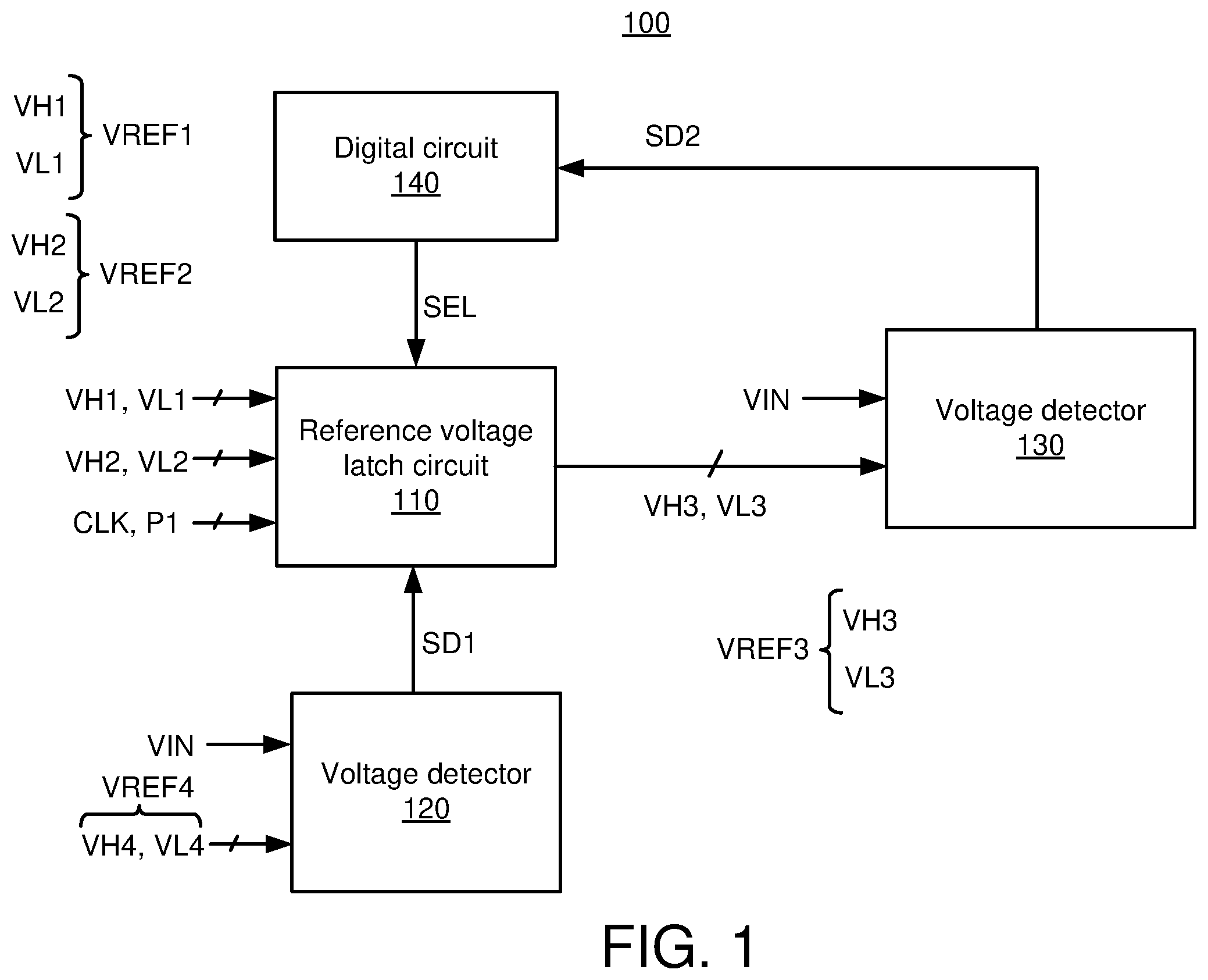
shows a schematic diagram of a voltage detection device 100 according to some embodiments of the present application. In some embodiments, the voltage detection device 100 may detect an input voltage VIN to prevent circuit system failure occurring in the event of such as a sudden shutdown. In some embodiments, the input voltage VIN may be used to drive a circuit system. For example, the input voltage VIN may be, for example but not limited to, a supply voltage of a digital circuit system, or a driving voltage used by an input/output interface circuit system.
The voltage detection device 100 includes a reference voltage latch circuit 110 , a voltage detector 120 , a voltage detector 130 and a digital circuit 140 . The reference voltage latch circuit 110 may output one of a first set of reference voltages VREF 1 and a second set of reference voltages VREF 2 as a third set of reference voltages VREF 3 according to a selection signal SEL, wherein the first set of reference voltages VREF 1 are lower than the second set of reference voltages VREF 2 . For example, the first set of reference voltages VREF 1 include a voltage VH 1 and a voltage VL 1 , and the second set of reference voltages VREF 2 include a voltage VH 2 and a voltage VL 2 . The voltage VH 1 is higher than the voltage VL 1 and lower than the voltage VH 2 , and the voltage VL 2 is lower than the voltage VH 2 and higher than the voltage VL 1 . For example, the voltage VH 2 may be set to be approximately 1.58 V, the voltage VL 2 may be set to be approximately 1.44 V, the voltage VH 1 may be set to be approximately 1.34 V, and the voltage VL 1 may be set to be approximately 1.3 V. It should be noted that the above numerical values of the voltages are merely examples, and the present application is not limited to these examples. The reference voltage latch circuit 110 may output the voltage VH 1 and the voltage VL 1 as a voltage VH 3 and a voltage VL 3 of the third set of reference voltages VREF 3 according to the selection signal SEL, respectively, or output the voltage VH 2 and the voltage VL 2 as the voltage VH 3 and the voltage VL 3 , respectively.
The reference voltage latch circuit 110 may store (or latch) the selection signal SEL as a switching signal (for example, a switching signal SW in ) according to a clock signal CLK and a predetermined value P 1 corresponding to the input voltage VIN, and output the third set of reference signals VREF 3 according to the switching signal. Moreover, the reference voltage latch circuit 110 may be selectively to be reset according to a detection signal SD 1 , or to continue outputting the one of the first set of reference voltages VREF 1 and the second set of reference voltages VREF 2 as the third set of reference voltages VREF 3 . For example, if the detection signal SD 1 indicates that the input voltage VIN is not lower than a fourth set of reference voltages VREF 4 to be described below (for example, if the fourth set of reference voltages VREF 4 are equal to the first set of reference voltages VREF 1 , the condition herein means that the input voltage VIN is not lower than a lower limit of the first set of reference voltages VREF 1 , that is, the voltage VL 1 ), the reference voltage latch circuit 110 may continue outputting the set of reference voltages previous selected (for example, the second set of reference voltages VREF 2 ) as the third set of reference voltages VREF 3 . Alternatively, if the detection signal SD 1 indicates that the input voltage VIN is lower than the fourth set of reference voltages VREF 4 to be described below (for example, if the fourth set of reference voltages VREF 4 are equal to the first set of reference voltages VREF 1 , the condition herein means that the input voltage VIN is lower than the voltage VL 1 ), the reference voltage latch circuit 110 may be reset so as to clear internal circuit settings to re-select set of reference voltages. Operation details related to the reference voltage latch circuit 110 are described with reference to and/or below.
The voltage detector 120 may compare the input voltage VIN with a fourth set of reference voltages VREF 4 to generate the detection signal SD 1 . In some embodiments, if part of circuits in the system are configured to operate at a lower voltage, the fourth set of reference voltages VREF 4 may be set to be lower than the first set of reference voltages VREF 1 ; for example, an upper limit of the fourth set of reference voltages VREF 4 is lower than the voltage VH 1 and a lower limit of the fourth set of reference voltages VREF 4 is lower than the voltage VL 1 . In some embodiments, the upper limit of the fourth set of reference voltages VREF 4 may be set to be 0.6 to 0.9 (for example, to be approximately 0.75) times of the voltage VH 1 , and the lower limit of the fourth set of reference voltages VREF 4 may be set to be 0.6 to 0.9 (for example, to be approximately 0.75) times of the voltage VL 1 . In some embodiments, the fourth set of reference voltage VREF 4 may be set to be equal to the first set of reference voltages VREF 1 . For better understanding, in the embodiments to be described below, the fourth set of reference voltages VREF 4 are equal to the first set of reference voltages VREF 1 as an example; however, it should be noted that the present invention is not limited to the example. When the fourth set of reference voltages VREF 4 are equal to the first set of reference voltages VREF 1 , the voltage detector 120 may compare the input voltage VIN with the first set of reference voltages VREF 1 (in other embodiments, this may be replaced by another set of voltages lower than the first set of reference voltages VREF 1 ) so as to generate the detection signal SD 1 . The detection signal SD 1 may indicate whether the input voltage VIN is higher than the voltage VH 1 or lower than the voltage VL 1 . Similarly, the voltage detector 130 may generate a detection signal SD 2 according to the third set of reference voltages VREF 3 and the input voltage VIN. For example, the voltage detector 130 may compare the input voltage VIN with the third set of reference voltages VREF 3 to generate the detection signal SD 2 . The detection signal SD 2 may indicate whether the input voltage VIN is higher than the voltage VH 2 or lower than the voltage VL 2 . If the input voltage VIN is higher than the voltage VH 2 , it means that the input voltage VIN has risen to a target level and approximates a stable state.
The digital circuit 140 generates the selection signal SEL according to the second detection signal SD 2 . In some embodiments, the digital circuit 140 is further controlled by software (or firmware) in the system, so as to switch the selection signal SEL under a predetermined condition. In some embodiments, the digital circuit 140 is disposed in an electronic device including the voltage detection device 100 , and is, for example, a control circuit or a central processor. In some embodiments, the digital circuit 140 may include registers storing control values or parameters, so as to control the operation of the voltage detection device 100 . Associated details of the predetermined condition for switching the selection signal SEL are to be described with reference to below.
shows a waveform diagram of multiple signals in according to some embodiments of the present application. In an initial stage (for example, when the system is initially activated), the digital circuit 140 outputs the selection signal SEL (not shown) having a first value (for example, logic 0), such that the reference voltage latch circuit 110 outputs the first set of reference voltages VREF 1 as the third set of reference voltages VREF 3 . In this case, the level of the voltage VH 3 is equal to that of the voltage VH 1 , and the level of the voltage VL 3 is equal to that of the voltage VL 1 . At a timing t 1 , the input voltage VIN begins to be higher than the voltage VH 3 , such that the detection signal SD 1 and the detection signal SD 2 both switch from a low level (corresponding to logic 0) to a high level (corresponding to logic 1). At a timing t 2 , with the control of software or firmware in the system, the digital circuit 140 outputs the selection signal SEL having a second value (for example, logic 1), such that the reference voltage latch circuit 110 switches to output the second set of reference voltages VREF 2 as the third set of reference voltages VREF 3 according to the selection signal SEL. In this case, the level of the voltage VH 3 rises to that of the voltage VH 2 , and the level of the voltage VL 3 rises to that of the voltage VL 2 . In other words, if the detection signal SD 2 satisfies a predetermined condition (for example, the detection signal SD 2 has a predetermined level (for example, a high level) within a predetermined period (for example, a period between the timing t 1 and the timing t 2 ) after the reference voltage latch circuit 110 outputs the first set of reference voltages VREF 1 as the third set of reference voltages VREF 3 ), the software or firmware in the system controls the digital circuit 140 to adjust the selection signal SEL, such that the reference voltage latch circuit 110 switches to output the second set of reference voltages VREF 2 as the third set of reference voltages VREF 3 .
Next, at a timing t 3 , due to influences of factors such as a sudden shutdown, the input voltage VIN is lower than the voltage VL 3 (for example, lower than the voltage VL 2 but not lower than the voltage VL 1 ). In this case, the detection signal SD 2 switches to having a low level so as to notify the circuit system to be reset to further prevent failure of the circuit system. Meanwhile, because the input voltage VIN is not lower than the voltage VL 1 , the detection signal SD 1 is still kept at a high level. In this case, the reference voltage latch circuit 110 may continue outputting the second set of reference voltages VREE 2 as the third set of reference voltages VREF 3 . As such, it is ensured that an erroneous operation or failure of the circuit system resulted by a voltage drop of this voltage is not incurred. At a timing t 4 , the input voltage VIN is again higher than the voltage VH 3 , such that the detection signal SD 2 switches to be at a high level. Thus, the circuit system may continue the original operation. On the other hand, if the input voltage VIN is lower than the voltage VL 3 and the voltage VL 1 at the timing t 3 , the detection signal SD 1 and the detection signal SD 2 are both switched to a low level. In this case, it means that the level of the input voltage VIN is too low, and the reference voltage latch circuit 110 may be reset (for example, clearing internal circuit settings) according to the detection signal SD 1 , so as to re-select a set of reference voltages in the next operation and accordingly output the third set of reference voltages VREF 3 .
In some related art, the voltage detection mechanism in an electronic device uses merely one set of reference voltages (for example, the second set of reference voltages VREF 2 ) to determine whether an input voltage suddenly drops. However, if the voltage drop of the input voltage is not significant enough (for example, the input voltage VIN is lower than the voltage VH 2 but higher than the voltage VL 2 ), the voltage detection mechanism may still mistakenly determine that the input voltage has a normal level and hence does not perform other operations. In fact, failure of the actual circuit system or an error signal may be resulted because of such voltage drop. Compared to the art above, in some embodiments of the present invention, the voltage detection device 100 uses two sets of reference voltages, and switches to use a reference voltage having a higher level within a period after power-on so as to determine whether the above voltage drops occurs in the input voltage VIN. As such, whether a voltage drop occurs in the input voltage VIN can be more accurately determined to thereby prevent system failure.
shows a schematic diagram of the reference voltage latch circuit 110 in according to some embodiments of the present application. The reference voltage latch circuit 110 includes a trigger 310 , a flip-flop 320 and a multiplexer 330 . The trigger 310 generates a trigger signal ST according to the clock signal CLK and the predetermined value P 1 . In some embodiments, the predetermined value P 1 may be a target level of the input voltage VIN. For example, if the input voltage VIN is predetermined to be 1.8 V at a stable state, the predetermined value P 1 may be 1.8 V. The trigger 310 includes a NAND gate 311 and an inverter 312 . The NAND gate 311 generates a signal S 1 according to the clock signal CLK and the predetermined value P 1 . The inverter 312 generates a trigger signal ST according to the signal S 1 .
The flip-flop 320 outputs the selection signal SEL as the switching signal SW according to the trigger signal ST, and selectively continues outputting the selection signal SEL as the switching signal SW or resets the switching signal SW according to the detection signal SD 1 . For example, the flip-flop 320 may be a D flip-flop having a reset input terminal (denoted as R), wherein the reset input terminal receives the detection signal SD 1 . When the detection signal SD 1 has a high level, the flip-flop 320 may sequentially output the selection signal SEL as the switching signal SW according to the trigger signal ST. When the detection signal SD 1 has a low level, the flip-flop 320 may reset the switching signal SW (for example, resetting the signal value of the switching signal SW to logic 0). On the other hand, as shown in , when the input voltage VIN is lower than the voltage VL 2 but not lower than the voltage VL 1 , the detection signal SD 1 still has a high level. As such, the flip-flop 320 may continue outputting the selection signal SEL as the switching signal SW according to the trigger signal ST. In other words, when the input voltage VIN is not too low (that is, not lower than the voltage VL 1 ), the flip-flop 320 may continue latching the selection signal SEL as the switching signal SW. When the input voltage VIN becomes too low (that is, lower than the voltage VL 1 ), the detection signal SD 1 has a low level such that the flip-flop 320 resets the signal value of the switching signal SW.
The multiplexer 330 may output the first set of reference voltages VREF 1 or the second set of reference voltages VREF 2 as the third set of reference voltages VREF 3 according to the switching signal SW. For example, the multiplexer 330 includes multiple switches. Part of the switches are turned on when the switching signal SW is logic 0 so as to output the voltage VH 1 as the voltage VH 3 and to output the voltage VL 1 as the voltage VL 3 . The remaining part of the switches are turned on when the switching signal SW is logic 1 so as to output the voltage VH 2 as the voltage VH 3 and to output the voltage VL 2 as the voltage VL 3 .
shows a schematic diagram of the voltage detector 130 in according to some embodiments of the present application. In this example, the voltage detector 130 includes a comparator 410 , a comparator 420 and a latch 430 . The comparator 410 may compare the input voltage VIN with the voltage VH 3 to generate a setting signal SS. The comparator 420 may compare the input voltage VIN with the voltage VL 3 to generate a reset signal SR. The latch 430 may generate the detection signal SD 2 according to the setting signal SS and the reset signal SR. For example, the latch 430 may be an S-R latch, which is configured to have an input terminal thereof (denoted as S) receive the setting signal SS and a reset input terminal thereof (denoted as R) receive the reset signal SR. As such, when the input voltage VIN is higher than the voltage VH 3 , the latch 430 may output the detection signal SD 2 having a high level. Or, when the input voltage VIN is lower than the voltage VL 3 , the latch 430 may output the detection signal SD 2 having a low level.
shows a schematic diagram of the voltage detector 130 in according to some embodiments of the present application. In this example, the voltage detector 130 includes a multiplexer 510 and a comparator 520 . The multiplexer 510 selectively outputs the voltage VH 3 or the voltage VL 3 as a voltage V 3 according to the detection signal SD 2 . For example, the multiplexer 510 includes a first switch and a second switch. When the detection signal SD 1 has a low level (or example, logic 0), the first switch is turned on so as to output the voltage VH 3 as the voltage V 3 . Or, when the detection signal SD 1 has a high level (or example, logic 1), the second switch is turned on so as to output the voltage VL 3 as the voltage V 3 . The comparator 520 may compare the input voltage VIN with the voltage V 3 to generate the detection signal SD 2 . As such, the detection signal SD 2 may have a high level when the input voltage VIN is higher than the voltage VH 3 . Or, the detection signal SD 2 may have a low level when the input voltage VIN is lower than the voltage VL 3 .
In some embodiments, the implementation of the voltage detector 120 may be referred from the voltage detectors 130 in and . For example, to implement the voltage detector 120 , the voltage VH 3 in and may be replaced by the voltage VH 1 and the voltage VL 3 may be replaced by the voltage VL 1 (or replaced by another set of reference voltages lower than the first set of reference voltages VREF 1 ). Other operation and configuration details are the same as those of the examples in and , and are omitted herein for brevity.
shows a flowchart of a method 600 for preventing system failure according to some embodiments of the present application. In operation S 610 , one of a first set of reference voltages and a second set of reference voltages are output as a third set of reference voltages according to a selection signal, wherein the first set of reference voltages are lower than the second set of reference voltages. In operation S 620 , resetting or continuing outputting the one of the first set of reference voltages and the second set of reference voltages as the third set of reference voltages is selectively performed according to a first detection signal. In operation S 630 , a fourth set of reference voltages are compared with an input voltage to generate the first detection signal, wherein the input voltage is used to drive a circuit system and the fourth set of reference voltages are lower than or equal to the first set of reference voltages. In operation S 640 , the third set of reference voltages are compared with the input voltage to generate a second detection signal. In operation S 650 , a selection signal is generated according to the second detection signal.
The details of the plurality of operations above may be referred from the description associated with the foregoing embodiments, and are omitted herein for brevity. The plurality operations of the above method 600 for preventing system failure are merely examples, and are not limited to being performed in the order specified in these examples. Without departing from the operation means and ranges of the various embodiments of the present application, additions, replacements, substitutions or omissions may be made to the operations of the method 600 for preventing system failure, or the operations may be performed in different orders (for example, simultaneously performed or partially simultaneously performed).
In conclusion, the voltage detection device and the method for preventing system failure in some embodiments of the present invention are capable of improving voltage detection accuracy by using multiple sets of reference voltages, and latching a currently used reference voltage by using a circuit concept such as a latch circuit. Thus, it is ensured that the circuit system can be correctly reset in the event of a sudden voltage drop, thereby ensuring that failure in operations of the circuit system is not resulted.
While the present application has been described by way of example and in terms of the preferred embodiments, it is to be understood that the disclosure is not limited thereto. Various modifications made be made to the technical features of the present application by a person skilled in the art on the basis of the explicit or implicit disclosures of the present application. The scope of the appended claims of the present application therefore should be accorded with the broadest interpretation so as to encompass all such modifications.
Figures (5)
Citations
This patent cites (3)
- US2014/0285239
- US2015/0185745
- US2020/0202902