Abstract
A method for forming a photomask includes the following steps. A first target pattern is provided, wherein the first target pattern includes a first pattern area and a second pattern area. The first pattern area includes a block pattern. The second pattern area includes multiple stripe patterns. A first sidewall reset area is defined in the second pattern area. A retarget procedure is executed on the first target pattern to obtain a second target pattern. The photomask is formed based on the second target pattern.
Claims (13)
1. A method for forming a photomask, comprising: providing a first target pattern, wherein the first target pattern comprises: a first pattern area, comprising a block pattern with a width P 1 ; and a second pattern area, comprising a plurality of stripe patterns, wherein the stripe patterns are arranged along a direction away from the first pattern area, a width of each of the stripe patterns is P 2 , and P 1 is greater than P 2 ; defining a first sidewall reset area in the second pattern area; executing a retarget procedure on the first target pattern to obtain a second target pattern, wherein the retarget procedure comprises: retracting a sidewall of the block pattern facing one side of the adjacent stripe pattern; and expanding sidewalls of at least part of the stripe patterns in the first sidewall reset area toward the adjacent stripe patterns or the adjacent block pattern; and forming the photomask based on the second target pattern.
Show 12 dependent claims
2. The method for forming the photomask according to claim 1 , wherein forming the photomask based on the second target pattern comprises: correcting the second target pattern based on an optical proximity effect correction model; and transferring the corrected second target pattern onto a photomask material to form the photomask.
3. The method for forming the photomask according to claim 1 , wherein a part of the stripe patterns overlaps with the first sidewall reset area, and another part of the stripe patterns does not overlap with the first sidewall reset area.
4. The method for forming the photomask according to claim 1 , further comprising: setting a minimum pattern width P A and a minimum stripe pattern distance S A of an exposure process applicable to the photomask.
5. The method for forming the photomask according to claim 4 , wherein P A and S A are defined as: a limit width of the stripe pattern and a limit distance between the stripe patterns on the photomask when forming more than 25 continuously arranged stripe photoresists by the exposure process on the premise that the stripe photoresist has a minimum width and there is a minimum spacing between the stripe photoresists.
6. The method for forming the photomask according to claim 4 , wherein in the first target pattern, the width P 2 of each of the stripe patterns is less than 1.09 times P A and greater than or equal to P A .
7. The method for forming the photomask according to claim 4 , wherein in the first target pattern, another side of the first pattern area opposite to the second pattern area comprises a depletion region, wherein a width of the depletion region is greater than or equal to 4(P A +S A ), wherein the depletion region does not comprise any structure or the depletion region comprises a polygonal pattern with a width P 3 less than 0.6 times P A .
8. The method for forming the photomask according to claim 4 , wherein a width of the first sidewall reset area is equal to 4(P A +S A ).
9. The method for forming the photomask according to claim 4 , wherein the retarget procedure further comprises: selecting an effective sidewall among sidewalls of the stripe pattern overlapping with the first sidewall reset area, wherein a length of the effective sidewall is greater than 3 times P A , and a distance between the effective sidewall and the adjacent block pattern or the adjacent stripe pattern is less than 1.09 times S A and greater than or equal to S A ; and expanding the effective sidewall of the stripe pattern toward the adjacent stripe pattern or the block pattern.
10. The method for forming the photomask according to claim 4 , wherein in the retarget procedure, the effective sidewall of the stripe pattern closest to the first pattern area expands by a distance A toward the first pattern area, and the effective sidewalls of the other stripe patterns in the first sidewall reset area expand by a distance B toward the adjacent stripe patterns, wherein A is greater than B.
11. The method for forming the photomask according to claim 10 , further comprising: setting a minimum pattern width P A and a minimum stripe pattern distance S A of an exposure process applicable to the photomask, wherein A is greater than 14.5% of P A and B is greater than 9.1% of P A .
12. The method for forming the photomask according to claim 1 , wherein a distance between the stripe patterns in the first sidewall reset area is reduced after the retarget procedure.
13. The method for forming the photomask according to claim 1 , further comprising: defining a second sidewall reset area in the second pattern area, wherein the first sidewall reset area is located between the second sidewall reset area and the first pattern area, wherein the retarget procedure further comprises: expanding sidewalls of another part of the stripe patterns in the second sidewall reset area toward the adjacent stripe patterns, wherein an extent of expansion is less than an extent to which the sidewalls of at least part of the stripe patterns in the first sidewall reset area are expanded toward the adjacent stripe patterns or the block pattern.
Full Description
Show full text →
CROSS-REFERENCE TO RELATED APPLICATION
This application claims the priority benefit of Taiwan application serial no. 111138201, filed on Oct. 7, 2022. The entirety of the above-mentioned patent application is hereby incorporated by reference herein and made a part of this specification.
BACKGROUND
Technical Field
The disclosure relates to a method for forming a photomask.
Description of Related Art
In recent years, various semiconductor elements are all developing toward the direction of area reduction, and one of the most critical processes that determines the area of the semiconductor element is the photolithography process. The critical dimension (CD) of various structures in the semiconductor element is determined by the photolithography process. Therefore, in order to reduce the area of the semiconductor element, it is necessary to improve the related technology of the photolithography process.
Generally speaking, the target CD of the developed pattern on the photoresist layer is an important factor in determining the resolution of the photolithography process. At present, in order to reduce the target CD of the developed pattern, a light source with a short wavelength may be used for exposure. However, as the target CD shrinks, the requirements for the precision of the photolithography process must increase.
SUMMARY
The disclosure provides a method for forming a photomask, and the formed photomask can improve the precision of a lithography process.
At least one embodiment of the disclosure provides a method for forming a photomask, which includes the following steps. A first target pattern is provided. The first target pattern includes a first pattern area and a second pattern area. The first pattern area includes a block pattern with a width P 1 . The second pattern area includes multiple stripe patterns. The stripe pattern is arranged along a direction away from the first pattern area. A width of each of the stripe patterns is P 2 , and P 1 is greater than P 2 . A first sidewall reset area is defined in the second pattern area. A retarget procedure is executed on the first target pattern to obtain a second target pattern. The retarget procedure includes retracting a sidewall of one side of the block pattern facing the adjacent stripe pattern; and expanding sidewalls of at least part of the stripe patterns in the first sidewall reset area toward the adjacent stripe patterns or the adjacent block pattern. The photomask is formed based on the second target pattern.
BRIEF DESCRIPTION OF THE DRAWINGS
is a schematic top view of a photomask according to an embodiment of the disclosure.
A to C are schematic views of a method for forming a photomask according to an embodiment of the disclosure.
is a schematic view of a method for forming a photomask according to an embodiment of the disclosure.
A and B are schematic views of optical proximity correction (OPC) of a photomask according to an embodiment of the disclosure.
is a flowchart of a method for forming a photomask according to an embodiment of the disclosure.
DETAILED DESCRIPTION OF DISCLOSED EMBODIMENTS
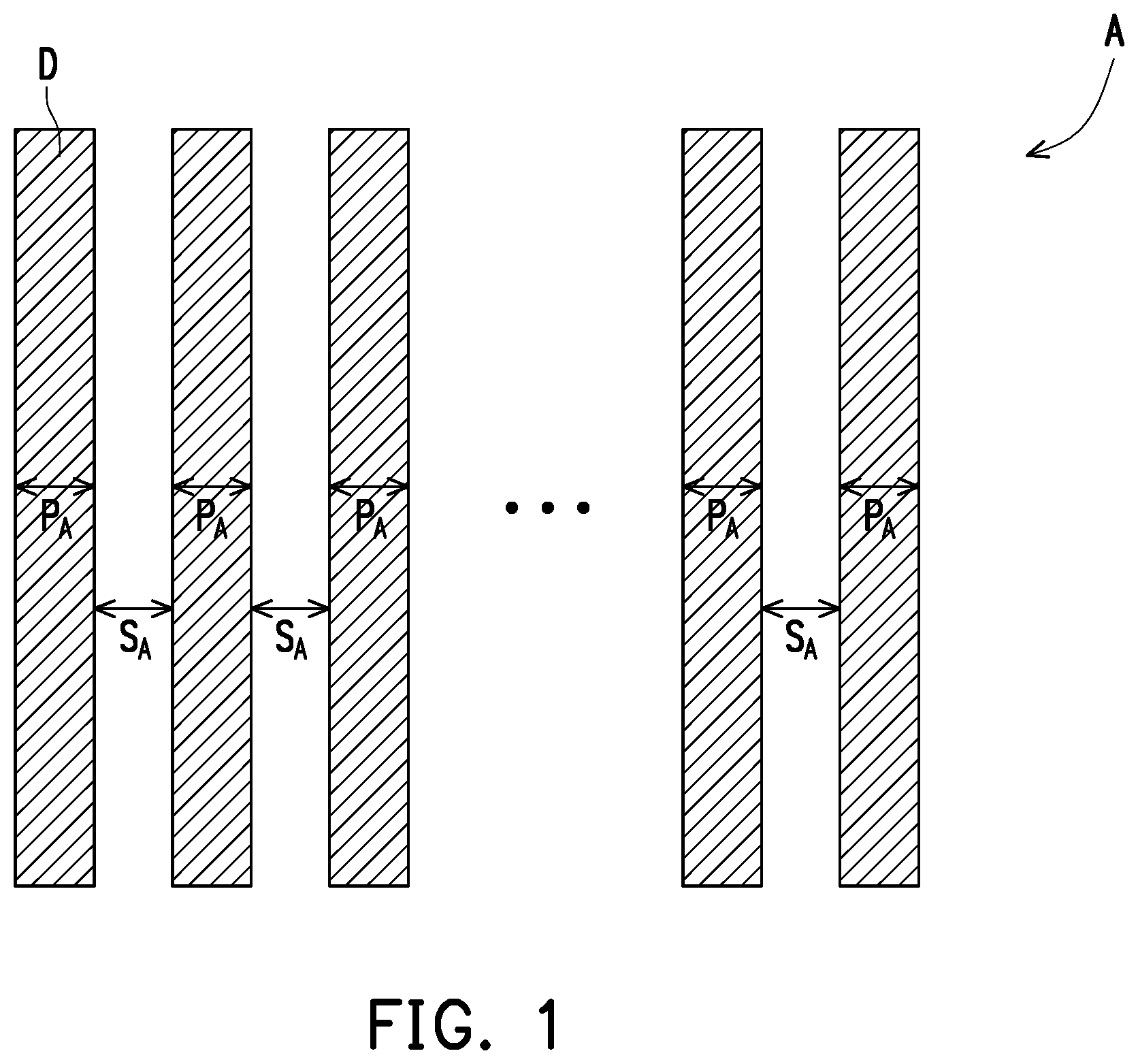
is a schematic top view of a photomask according to an embodiment of the disclosure. Specifically, is used to illustrate a minimum pattern width P A and a minimum stripe pattern distance S A of an exposure process applicable to a photomask A. The minimum pattern width P A and the minimum stripe pattern distance S A may be interpreted as the width of a pattern and the distance between patterns on the photomask A when a target photoresist pattern has the maximum resolution.
Please refer to . In some embodiments, in order to obtain the minimum pattern width P A and the minimum stripe pattern distance S A of the exposure process applicable to the photomask A, the photomask A including more than 25 continuously arranged stripe structures D is formed, and the stripe structure D has the minimum pattern width P A and the minimum stripe pattern distance S A . Next, the exposure process and a development process are performed on a photoresist (not shown) using the photomask A, so as to form more than 25 continuously arranged stripe photoresists (not shown). Under the premise that the stripe photoresist has a minimum width and there is a minimum spacing between the stripe photoresists, the width of the stripe pattern D and the distance between the stripe patterns D on the photomask A are respectively the minimum pattern width P A and the minimum stripe pattern distance S A .
In some embodiments, the minimum pattern width P A and the minimum stripe pattern distance S A are obtained using the aforementioned method in an experimental or simulated manner, but the disclosure is not limited thereto. In other embodiments, other manners may also be adopted to calculate the minimum pattern width P A and the minimum stripe pattern distance S A of the photomask A.
The minimum pattern width P A and the minimum stripe pattern distance S A on the photomask A vary depending on the equipment used for the exposure process of the photomask A. For example, when a light source with a reduced wavelength is used for exposure, the actual values of the minimum pattern width P A and the minimum stripe pattern distance S A on the photomask A will decrease accordingly.
A to C are schematic views of a method for forming a photomask according to an embodiment of the disclosure, wherein the patterns shown in A to C are used to illustrate each step of designing the shape of the photomask in design software, simulation software, or correction software. In other words, the patterns shown in A to C are stored in a memory or other storage media in the form of, for example, data, patterns, or other forms.
Please refer to A . A first target pattern 10 is provided. The first target pattern 10 includes a first pattern area 110 and a second pattern area 120 . In some embodiments, the first target pattern 10 optionally further includes a depletion region 130 . The first pattern area 110 is located between the second pattern area 120 and the depletion region 130 . In other words, the other side of the first pattern area 110 opposite to the second pattern area 120 optionally includes the depletion region 130 .
The first pattern area 110 includes a block pattern 112 with a width P 1 . The second pattern area 120 includes multiple stripe patterns 122 , wherein the width of each of the stripe patterns 122 is P 2 . In the embodiment, P 1 is greater than P 2 . In the embodiment, the block pattern 112 and the stripe pattern 122 are parallel to each other and both extend along a first direction D 1 . The stripe patterns 122 are arranged along a second direction D 2 away from the first pattern area 110 .
The minimum pattern width P A and the minimum stripe pattern distance S A of the photomask are obtained by the method and the related description of or other methods. In some embodiments, the width P 2 of each of the stripe patterns 122 in the first target pattern 10 is less than 1.09 times P A and greater than or equal to P A . In some embodiments, the width P 1 of the block pattern 112 in the first target pattern 10 is greater than 1.4 times P A .
In some embodiments, the depletion region 130 does not include any structure or the structure in the depletion region 130 is not transferred onto a photoresist pattern after a photolithography process due to the very small size. For example, the depletion region 130 includes a polygonal pattern 132 with a width P 3 less than 0.6 times P A . In some embodiments, a width 130 W of the depletion region 130 is greater than or equal to 4(P A +S A ).
A first sidewall reset area RT 1 is defined in the second pattern area 120 . In some embodiments, the first sidewall reset area RT 1 is located on one side of the first pattern area 110 and overlaps with several stripe patterns 122 in the second pattern area 120 that are closest to the first pattern area 110 . In some embodiments, a width RTW of the first sidewall reset area RT 1 is equal to 4(P A +S A ). In the embodiment, a part of the stripe patterns 122 overlaps with the first sidewall reset area RT 1 , and another part of the stripe patterns 122 does not overlap with the first sidewall reset area RT 1 , but the disclosure is not limited thereto. In other embodiments, all the stripe patterns 122 overlap with the first sidewall reset area RT 1 .
Next, please refer to B and C . A retarget procedure is executed on the first target pattern 10 to obtain a second target pattern 10 ′. In some embodiments, the retarget procedure includes intercepting an effective sidewall of the block pattern 112 and/or the stripe pattern 122 , and then moving the effective sidewall of the block pattern 112 and/or the stripe pattern 122 . For example, the retarget procedure includes retracting a sidewall 112 s of one side of the block pattern 112 facing the adjacent stripe pattern 122 , and expanding sidewalls 122 s of at least part of the stripe patterns 122 in the first sidewall reset area RT 1 toward the adjacent stripe patterns 122 or the adjacent block pattern 112 .
For example, please refer to B . An effective sidewall among the sidewalls 122 s of the stripe patterns 122 overlapping with the first sidewall reset area RT 1 and an effective sidewall among the sidewalls 112 s of the block pattern 112 are selected. The length of the effective sidewall in the first direction D 1 is greater than 3 times P A , and the distance between the effective sidewall and the adjacent block pattern 112 or the adjacent stripe pattern 122 is less than 1.09 times S A and greater than 1 times S A . In the embodiment, in the first target pattern 10 , a distance S 1 between the block pattern 112 and the adjacent stripe pattern 122 and a distance S 2 between the two adjacent stripe patterns 122 are both less than 1.09 times S A and greater than or equal to 1 times S A .
In B , the effective sidewall of the block pattern 112 and/or the stripe pattern 122 is indicated by a thick line. In the embodiment, the sidewalls 122 s of each stripe pattern 122 overlapping with the first sidewall reset area RT 1 are effective sidewalls, but the disclosure is not limited thereto. In other embodiments, the sidewalls 122 s of a part of the stripe patterns 122 overlapping with the first sidewall reset area RT 1 are not effective sidewalls.
After determining the effective sidewall among the sidewalls 122 s of the stripe pattern 122 and the effective sidewall among the sidewalls 112 s of the block pattern 112 , the effective sidewall of the block pattern 112 and/or the stripe pattern 122 is moved to obtain the second target pattern 10 ′ including a block pattern 112 a , a stripe pattern 122 a , and the stripe pattern 122 , as shown in C . In the embodiment, the second target pattern 10 ′ further includes the stripe pattern 122 with the sidewalls not moved and the depletion region 130 .
In the embodiment, the effective sidewall of the block pattern 112 is retracted toward a direction away from the stripe pattern 122 and parallel to the second direction D 2 , so as to form the block pattern 112 a with a width P 1 ′. For example, the effective sidewall of the block pattern 112 is retracted by 2.5 nm.
In addition, each effective sidewall of the stripe pattern 122 expands along a direction parallel to the second direction D 2 . For example, the sidewall 122 s (the effective sidewall) of the stripe pattern 122 closest to the first pattern area 110 expands by a distance A toward the first pattern area 110 , and the sidewalls 122 s (the effective sidewalls) of the other stripe patterns 122 in a first sidewall reset area RT expand by a distance B toward the adjacent stripe patterns 122 . In some embodiments, since the sidewall of the block pattern 112 facing one side of the stripe pattern 122 is retracted, the sidewall of one side of the stripe pattern 122 closest to the block pattern 112 facing the block pattern 112 has a larger expansion space. Therefore, in some embodiments, A is greater than B. In other words, the distance A of the stripe pattern 122 closest to the block pattern 112 expanding to the left is greater than the distance B of expanding to the right, and the stripe pattern 122 a is formed after the expansion. The distance B of the other stripe patterns 122 in the first sidewall reset area RT expanding to the left is equal to the distance B of expanding to the right. In some embodiments, A is greater than 14.5% of P A and B is greater than 9.1% of P A . In the embodiment, a width P 2 a ′ of the stripe pattern 122 a closest to the block pattern 112 a is greater than a width P 2 b ′ of the other stripe patterns 122 a.
In some embodiments, after executing the retarget procedure, a distance S 1 ′ between the stripe pattern 122 a and the block pattern 112 a is the same as or different from the distance S 1 (please refer to B ) before executing the retarget procedure. In addition, after executing the retarget procedure, a distance S 2 ′ between the two adjacent stripe patterns 122 a is less than the distance S 2 (please refer to B ) before executing the retarget procedure. Finally, the photomask is formed based on the second target pattern 10 ′.
Generally speaking, when the photomask is used for the exposure process, if the photomask includes a block pattern and multiple continuous stripe patterns adjacent to the block pattern, the exposure of the stripe pattern is easily affected by the block pattern, wherein the region of the stripe patterns close to the block pattern is most easily affected, which causes a decline in the accuracy of the photolithography process. In the disclosure, the first target pattern 10 (please refer to A ) is corrected to the second target pattern 10 ′ by the retarget procedure, so as to improve the issue of the decline in the accuracy of the photolithography process and enable the photoresist pattern obtained by the photolithography process to be closer to the original expected pattern (the first target pattern 10 ).
is a schematic view of a method for forming a photomask according to an embodiment of the disclosure. It must be noted here that the embodiment of continues to use the reference numerals and some content of the embodiment of A and B , wherein the same or similar reference numerals are adopted to represent the same or similar elements, and the description of the same technical content is omitted. For the description of the omitted part, reference may be made to the foregoing embodiment, which will not be repeated here.
In the embodiment of , the first sidewall reset area RT 1 and the second sidewall reset area RT 2 are defined in the second pattern area 120 , wherein the first sidewall reset area RT 1 is located between the second sidewall reset area RT 2 and the first pattern area 110 . In addition, in the embodiment, the depletion region 130 does not include any structure.
In the embodiment, in addition to moving at least part of the sidewalls of the block pattern 112 and/or the stripe patterns 122 in the first sidewall reset area RT 1 , the retarget procedure also moves at least part of the sidewalls of the stripe patterns 122 in the second sidewall reset area RT 2 , so as to obtain a second target pattern 10 a′.
In the embodiment, the sidewalls 122 s of another part of the stripe patterns 122 in the second sidewall reset area RT 2 are expanded toward the adjacent stripe patterns 122 to form stripe patterns 122 b . In some embodiments, the sidewall of the stripe pattern 122 / 122 b in the second sidewall reset area RT 2 is expanded to a lesser extent than the extent to which the sidewall 122 s of the stripe pattern 122 / 122 a in the first sidewall reset area RT 1 is expanded toward the adjacent stripe pattern 122 or block pattern 112 . Finally, the photomask is formed based on the second target pattern 10 a′.
A and B are schematic views of optical proximity correction of a photomask according to an embodiment of the disclosure. In the embodiment, forming the photomask based on the second target pattern 10 ′ includes the following steps. First, the second target pattern 10 ′ is corrected based on an optical proximity effect correction model. Next, a corrected second target pattern 10 ″ is transferred onto a photomask material to form the photomask. In some embodiments, for the method for forming the second target pattern 10 ′, reference may be made to the embodiment of A to C . In A , the depletion region 130 in C is omitted.
In the embodiment, if the first target pattern 10 (please refer to A ) is directly corrected based on the optical proximity effect correction model, the subsequent exposure to the stripe patterns 122 is easily affected by the block pattern 112 , which causes deviations in the photolithography process in the region of the stripe patterns close to the block pattern. In the embodiment, since the retarget procedure is first executed to correct the first target pattern 10 to the second target pattern 10 ′, and the second target pattern 10 ′ is then corrected based on the optical proximity effect correction model, the issue of the deviations in the photolithography process can be improved.
In some embodiments, compared to directly correcting the first target pattern 10 based on the optical proximity effect correction model, the stripe patterns 122 a obtained after correcting the second target pattern 10 ′ based on the optical proximity effect correction model have larger widths P 2 a ″ and P 2 b ″. For example, the width P 2 a ″ of the stripe pattern 122 a closest to the block pattern 112 a is greater than the width of the stripe pattern (not shown) obtained by directly correcting the first target pattern 10 based on the optical proximity effect correction model by more than 5%.
In addition, the width P 2 b ″ of the other stripe patterns 122 a corrected by the retarget procedure is greater than the width of the stripe pattern (not shown) obtained by directly correcting the first target pattern 10 based on the optical proximity effect correction model by more than 2.2%.
In some embodiments, a ¼ reduction exposure system is used in conjunction with the photomask including the corrected second target pattern 10 ″ to perform the photolithography process, a spacing of a stripe photoresist corresponding to the obtained stripe pattern 122 a is X 1 , and a distance between the two stripe photoresists corresponding to the two stripe patterns 122 a is X 2 . The ¼ reduction exposure system is used in conjunction with the photomask including the first target pattern (not shown) after OPC to perform the photolithography process, a spacing of a stripe photoresist corresponding to the obtained stripe pattern is Y 1 , and a distance between the two stripe photoresists corresponding to the two stripe patterns is Y 2 . In some embodiments, X 1 is approximately equal to Y 1 (the difference between the two is less than 1.5 nm), and X 2 is less than Y 2 (the difference between the two is greater than or equal to 1.5 nm).
is a flowchart of a method for forming a photomask according to an embodiment of the disclosure. The method for forming the photomask includes the following steps. In Step S 502 , a first target pattern is provided, as shown in A . In Step S 504 , a retarget procedure is executed on the first target pattern to obtain a second target pattern, as shown in B and C . In Step S 506 , the second target pattern is corrected based on an optical proximity effect correction model, as shown in A and B . Finally, in Step S 508 , the corrected second target pattern is transferred onto a photomask material to form the photomask.
In summary, the method for forming the photomask of the disclosure can improve the process margin of the photolithography process and can improve the issue that the pattern formed by the photolithography process is not precise enough.
Figures (7)
Citations
This patent cites (9)
- US8321818
- US11048161
- US2002/0182550
- US2003/0051225
- US2007/0231710
- US2019/0163049
- US108695184
- US1816517
- US201415159