Abstract
An electronic device includes a substrate and data lines, gate lines, spacers, a first light-shielding layer, a second light-shielding layer and a third light-shielding layer disposed on the substrate. The data lines and the gate lines respectively extend along a first direction and a second direction different from the first direction. The first light-shielding layer includes a plurality of first light-shielding elements arranged corresponding to the data lines respectively and extending along the first direction. The second light-shielding layer includes a plurality of second light-shielding elements arranged corresponding to the gate lines respectively and extending along the second direction. The third light-shielding layer is arranged corresponding to a part of the spacers. At the overlap of the first light-shielding layer, the second light-shielding layer and the third light-shielding layer, the first light-shielding layer, the second light-shielding layer and the third light-shielding layer have different the distances from the substrate respectively.
Claims (20)
1. An electronic device, comprising: a substrate; a plurality of data lines disposed on the substrate and extending along a first direction; a plurality of gate lines disposed on the substrate and extending along a second direction, wherein the first direction is different from the second direction; a plurality of spacers disposed on the substrate; a first light-shielding layer comprising a plurality of first light-shielding elements arranged corresponding to one of the plurality of data lines respectively and extending along the first direction; a second light-shielding layer comprising a plurality of second light-shielding elements arranged corresponding to one of the plurality of gate lines and extending along the second direction; and a third light-shielding layer arranged corresponding to at least one portion of the plurality of spacers; wherein at an overlap of the first light-shielding layer, the second light-shielding layer and the third light-shielding layer, the first light-shielding layer, the second light-shielding layer and the third light-shielding layer have different distances from the substrate respectively.
Show 19 dependent claims
2. The electronic device as claimed in claim 1 , wherein a width of one of the plurality of second light-shielding elements in the first direction is greater than a width of the corresponding one of the plurality of gate lines in the first direction.
3. The electronic device as claimed in claim 1 , wherein a width of one of the plurality of second light-shielding elements in the first direction is less than a width of the corresponding one of the plurality of gate lines in the first direction.
4. The electronic device as claimed in claim 1 , wherein the third light-shielding layer comprises a plurality of third light-shielding elements arranged corresponding one of the plurality of spacers respectively, and a maximum width of each of the plurality of third light-shielding elements in the first direction is greater than a width of a corresponding one of the plurality of spacers in the first direction.
5. The electronic device as claimed in claim 1 , further comprising a display medium layer disposed on the plurality of data lines and the plurality of gate lines, wherein the display medium layer is disposed between the first light-shielding layer, the second light-shielding layer, and the third light-shielding layer and the plurality of gate lines.
6. The electronic device as claimed in claim 5 , further comprising a fourth light-shielding layer disposed between the substrate and the plurality of gate lines.
7. The electronic device as claimed in claim 6 , wherein the fourth light-shielding layer comprises a plurality of four light-shielding elements arranged corresponding to one of the plurality of gate lines respectively and extending along the second direction.
8. The electronic device as claimed in claim 7 , wherein a width of each of the plurality of fourth light-shielding elements in the first direction is greater than a width of each of the plurality of gate lines in the first direction, a width of each of the plurality of second light-shielding elements in the first direction is greater than the width of each of the plurality of fourth light-shielding elements in the first direction.
9. The electronic device as claimed in claim 5 , wherein the third light-shielding layer comprises a plurality of third light-shielding elements arranged corresponding to one of the plurality of spacers respectively, and each of the plurality of third light-shielding elements has plural widths.
10. The electronic device as claimed in claim 1 , wherein the third light-shielding layer is disposed between the plurality of gate lines and the substrate.
11. The electronic device as claimed in claim 10 , wherein a width of each of the plurality of second light-shielding elements in the first direction is less than a width of a corresponding one of each of the plurality of gate lines in the first direction.
12. The electronic device as claimed in claim 1 , wherein the second light-shielding layer is disposed between the plurality of gate lines and the substrate.
13. The electronic device as claimed in claim 12 , wherein the third light-shielding layer comprises a plurality of third light-shielding elements extending along the second direction, one of the plurality of third light-shielding elements comprises a first portion and a second portion, wherein the first portion is arranged corresponding to one of the plurality of gate lines, the second portion is arranged corresponding to one of the plurality of spacers, a width of the first portion in the first direction is less than a width of the corresponding one of the plurality of gate lines in the first direction, and a width of the second portion in the first direction is greater than a width of the corresponding one of the plurality of spacers in the first direction.
14. The electronic device as claimed in claim 1 , further comprising a fourth light-shielding layer disposed corresponding to another portion of the plurality of spacers.
15. The electronic device as claimed in claim 14 , wherein the third light-shielding layer comprises a plurality of third light-shielding elements extending along the second direction, the fourth light-shielding layer comprises a plurality of fourth light-shielding elements extending along the second direction, and the plurality of third light-shielding elements and the plurality of fourth light-shielding elements are disposed alternately along the first direction.
16. The electronic device as claimed in claim 15 , wherein one of the plurality of third light-shielding elements has plural widths in the first direction, and one of the plurality of fourth light-shielding elements has plural widths in the first direction.
17. The electronic device as claimed in claim 1 , wherein the electronic device comprises a plurality of sub-pixels, the second light-shielding layer is disposed between the plurality of gate lines and the substrate, and each of the second light-shielding elements has a length in the second direction greater than twice of a pixel pitch of the plurality of sub-pixels in the second direction.
18. The electronic device as claimed in claim 1 , wherein the electronic device comprises a plurality of sub-pixels, and a spacing between any two adjacent light-shielding elements of the plurality of second light-shielding elements in the first direction is greater than a pixel pitch of the plurality of sub-pixels in the first direction.
19. The electronic device as claimed in claim 1 , wherein the third light-shielding layer comprises a plurality of third light-shielding elements extending along the second direction, and one of the plurality of third light-shielding elements has plural widths in the first direction.
20. The electronic device as claimed in claim 19 , wherein each of the third light-shielding elements comprises a first portion and a second portion, the first portion is disposed corresponding to one of the plurality of gate lines, and the second portion is disposed corresponding to one of the plurality of spacers, and a width of the first portion in the first direction is less than a maximum width of the second portion in the first direction.
Full Description
Show full text →
CROSS REFERENCE TO RELATED APPLICATION
This application claims the benefit of U.S. Provisional Application No. 63/452,443, filed on Mar. 16, 2023. The content of the application is incorporated herein by reference.
BACKGROUND OF THE DISCLOSURE
1. Field of the Disclosure
The present disclosure relates to an electronic device, and more particularly to an electronic device with display function.
2. Description of the Prior Art
In modern technology, displays or electronic devices containing display functions have been widely used in daily life. Generally speaking, a light-shielding layer with a specific pattern may be disposed in the electronic device to improve the contrast of the displayed image. However, when the resolution is required to increase continuously, it will be difficult to produce the light-shielding layer with predetermined pattern due to issues such as material limits, process requirements, material residues, etc., affecting the process yield, thereby increasing production costs.
SUMMARY OF THE DISCLOSURE
One of the objectives of the present disclosure is to provide an electronic device including a plurality of light-shielding layers having specific designed pattern, so as to increase the product yield, surface visual perception, and/or contrast of the electronic device.
The present disclosure electronic device includes a substrate, a plurality of data lines, a plurality of gate lines, a plurality of spacers, a first light-shielding layer, a second light-shielding layer and a third light-shielding layer. The data lines are disposed on the substrate and extend along a first direction. The gate lines are disposed on the substrate and extend along a second direction. The first direction is different from the second direction. The spacers are disposed on the substrate. The first light-shielding layer includes a plurality of first light-shielding elements arranged corresponding to one of the plurality of data lines respectively and extending along the first direction. The second light-shielding layer includes a plurality of second light-shielding elements arranged corresponding to one of the gate lines respectively and extending along the second direction. The third light-shielding layer is disposed corresponding to at least a portion of the spacers. At the overlap of the first light-shielding layer, the second light-shielding layer and the third light-shielding layer, the first light-shielding layer, the second light-shielding layer and the third light-shielding layer have different distance from the substrate respectively.
These and other objectives of the present disclosure will no doubt become obvious to those of ordinary skill in the art after reading the following detailed description of the embodiment that is illustrated in the various figures and drawings.
BRIEF DESCRIPTION OF THE DRAWINGS
is a schematic diagram of a partial top-view according to a first embodiment of the electronic device of the present disclosure.
is a schematic diagram of a partial sectional-view along the cross-sectional line A-A′ and the cross-sectional line C-C′ of the electronic device shown in .
is a schematic diagram of a partial top-view according to a second embodiment of the electronic device of the present disclosure.
is a schematic diagram of a partial sectional-view along the cross-sectional line D-D′ of the electronic device shown in .
is a schematic diagram of a partial top-view according to a third embodiment of the electronic device of the present disclosure.
is a schematic diagram of a partial top-view according to a fourth embodiment of the electronic device of the present disclosure.
is a schematic diagram of a partial top-view according to a fifth embodiment of the electronic device of the present disclosure.
is a schematic diagram of a partial top-view according to a sixth embodiment of the electronic device of the present disclosure.
is a schematic diagram of a partial top-view according to a seventh embodiment of the electronic device of the present disclosure.
Referring to , is a schematic diagram of a partial top-view according to an eighth embodiment of the electronic device of the present disclosure.
DETAILED DESCRIPTION
The contents of the present disclosure will be described in detail with reference to specific embodiments and drawings. It is noted that, for purposes of illustrative clarity and being easily understood by the readers, the following drawings may be simplified schematic diagrams, and elements therein may not be drawn to scale. The numbers and sizes of the elements in the drawings are just illustrative and are not intended to limit the scope of the present disclosure.
Certain terms are used throughout the specification and following claims to refer to particular elements. Those skilled in the art should understand that electronic equipment manufacturers may refer to an element by different names. This document does not intend to distinguish between elements that differ in name but not function.
In the following description and claims, the terms “include”, “comprise” and “have” are used in an open-ended fashion, and thus should be interpreted to mean “include, but not limited to . . . ”. When the terms “include”, “comprise” and/or “have” are used in this specification, they specify the presence of the features, regions, steps, operations and/or elements, but do not exclude the presence or addition of one or more other features, regions, steps, operations, elements and/or combinations thereof.
Ordinal numbers such as “first” and “second” in the specification and claims are used to distinguish/describe the elements in the claims. It does not mean that the claimed element has any previous ordinal numbers, nor does it mean the order of a certain element and another element, or the order in manufacturing method. The ordinal number is just used to make a claimed element with a certain name be clearly distinguishable from another claimed element with the same name.
Spatially relative terms, such as “above”, “under”, “left”, “right”, “front”, “behind” and the like, used in the following embodiments just refer to the directions in the drawings and are not intended to limit the present disclosure. It should be understood that the elements in the drawings may be disposed in any kind of formation known by one skilled in the related art to describe the elements in a certain way.
In addition, when an element or layer is described as being on or above another element or layer, it should be understood that the element or layer is directly on the another element or layer, and alternatively, another element or layer may be between the element or layer and the another element or layer (indirectly). On the contrary, when the element or layer is described as being directly on the another element or layer, it should be understood that there is no intervening element or layer between them. When an element is electrically connected or coupled to another element, it may include the case that there may be conductive lines or passive components (e.g. resistor, capacitor, etc.) between the element and the another element to electrically connect them. No other electrical component between the element and the another element.
In this disclosure, the thickness, length and width may be measured by optical microscopy (OM), and the thickness or length may be measured by scanning electron microscope (SEM), but not limited thereto. The doping concentration of dopant may be measured by SEM, transmission electron microscope (TEM), X-ray photoelectron spectroscopy (XPS), energy-dispersive X-ray spectroscopy (EDS) or secondary ion mass spectrometer (SIMS), but not limited thereto. In addition, any two values or directions used for comparison may have certain errors.
In the specification, the terms “approximately”, “about”, “substantially”, “roughly”, and “same” generally mean within 10%, 5%, 3%, 2%, 1%, or 0.5% of the reported numerical value or range. The quantity disclosed herein is an approximate quantity, that is, without a specific description of “approximately”, “about”, “substantially”, “roughly”, and “same”, the quantity may still include the meaning of “approximately”, “about”, “substantially”, “roughly”, and “same”.
The electronic device in the present disclosure may include, but is not limited to, a display device, a light-emitting device, a backlight device, a virtual reality (VR) device, an antenna device, a sensing device or a splicing device. The electronic device may be a bendable or flexible electronic device. The display device may be a non-self-luminous display device or a self-luminous display device. The antenna device may be a liquid crystal antenna device or a non-liquid-crystal antenna device, and the sensing device may be a sensing device for sensing capacitance, light, heat energy or ultrasonic waves, but not limited thereto. Electronic devices may include passive components and active components, such as capacitors, resistors, inductors, diodes and transistors. Diodes may include light emitting diodes or photodiodes. The light-emitting diode may include, for example, an inorganic light emitting diode, an organic light emitting diode (OLED), a mini LED, a micro LED or a quantum dot LED, but not limited thereto. The tiled device may be, for example, a display tiled device or an antenna tiled device, but not limited thereto. It should be noted that the electronic device may be any combination as mentioned above, but not limited thereto. In addition, the display device may be, for example, in a shape of rectangular, circular, polygonal, a shape with curved edges, a curved surface, or other suitable shapes. An electronic device may have a peripheral system such as a drive system, a control system, a light source system to support a display device, an antenna device, a wearable device (e.g. including augmented reality or virtual reality), a vehicle-mounted device (e.g. including vehicle windshield) or a tiled device.
It should be noted that in the following embodiments, the technical features of several different embodiments may be disassembled, replaced, recombined and mixed to complete other examples without departing from the spirit of the present disclosure.
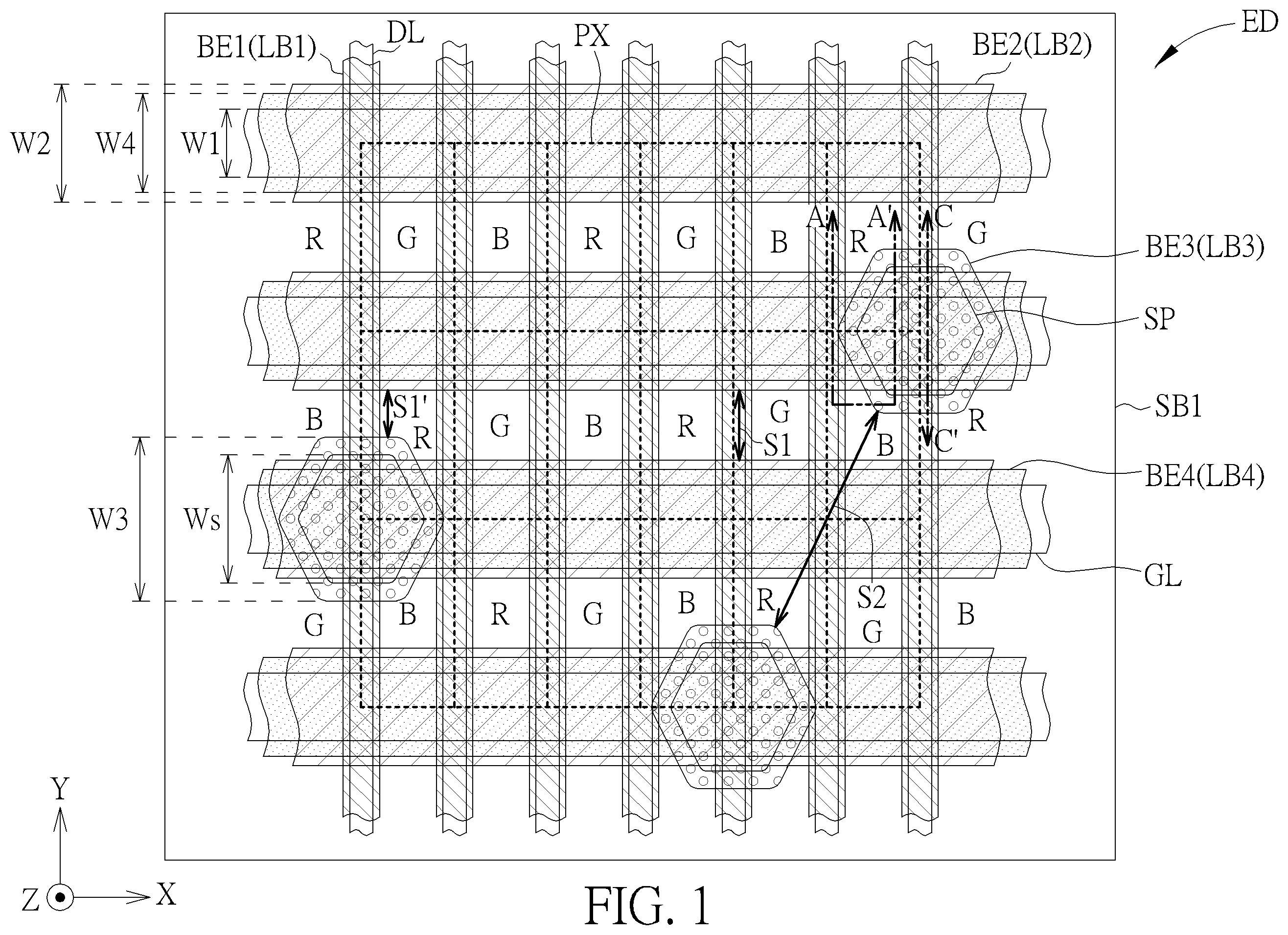
Referring to and , is a schematic diagram of a partial top-view according to a first embodiment of the electronic device of the present disclosure, and is a schematic diagram of a partial sectional-view along the cross-sectional line A-A′ and the cross-sectional line C-C′ of the electronic device shown in . In order to simplify the figure, a portion of elements of the electronic device are omitted in . The electronic device ED of the present disclosure includes a substrate SB 1 , at least one data lines DL, at least one gate lines GL, at least one spacer SP, and a plurality of light-shielding layers (such as the light-shielding layer LB 1 , the light-shielding layer LB 2 , the light-shielding layer LB 3 and the light-shielding layer LB 4 ), wherein the data line DL is disposed on the substrate SB 1 and extends along a first direction Y, the gate line GL is disposed on the substrate SB 1 and extends a long a second direction X, and the first direction Y is different from the second direction X. For example, the first direction Y may be perpendicular to the second direction X, but not limited thereto. In this embodiment, the electronic device ED includes a plurality of spacers SP, a plurality of data lines DL arranged parallel to each other and side by side, and a plurality of gate lines GL arranged parallel to each other and side by side. The gate lines GL and the data lines DL cross with each other to define a plurality of sub-pixels PX. When the electronic device ED has a display function, the area containing the sub-pixels PX may be regarded as the display region or active region of the electronic device ED, and the side of the substrate SB 1 where the gate lines GL and data lines DL are disposed (i.e., the upper side of ) may be regarded as the display side of the electronic device ED. Furthermore, each sub-pixel PX may correspond to a color individually, which means that it may emit light of a specific color, but not limited thereto. In the sub-pixels PX of the embodiment shown in , the letter “G” represents the green sub-pixel, the letter “B” represents the blue sub-pixel, and the letter “R” represents the red sub-pixel. In a lateral row, the green sub-pixels, blue sub-pixels and red sub-pixels are arranged in sequence alternately; in a straight line, the green sub-pixels, red sub-pixels and blue sub-pixels are arranged in sequence alternately, so three kinds of sub-pixels PX may appear in the same row or the same line. In this embodiment, a blue sub-pixel PX, a green sub-pixel PX and a red sub-pixel PX may compose one pixel. However, in variant embodiments, the numbers of different colors of sub-pixels PX in a single pixel may not be exactly the same. It should be noted that the color, type and arrangement of the sub-pixels PX included in the present disclosure electronic device ED are not limited to the above. The spacers SP are disposed on substrate SB 1 , and may be located on the side of the gate lines GL and data lines DL opposite to the substrate SB 1 . Specifically, the spacers SP may be disposed on the gate lines GL and/or data lines DL. There is a specific distance between two adjacent spacers SP. For example, two adjacent spacers SP will not be disposed in adjacent sub-pixels PX. The spacers SP may be substantially disposed at the intersection of the gate lines GL and the data lines DL. In other words, each spacer SP may overlap a portion of one gate line GL and a portion of one data line DL at the same time in a top-view direction, opposite to the third direction Z but parallel to the normal of substrate SB 1 , of the electronic device ED. The spacers SP may also be disposed at the intersection of different sub-pixels PX and partially overlap these sub-pixels PX respectively. The total area of all spacers SP overlapping the green sub-pixels PX may be less than the total area overlapping the blue sub-pixels PX and less than the total area overlapping the red sub-pixels PX, wherein this design may reduce the impact of spacers SP on the green sub-pixels PX and improve the visual perception. The arrangement location of the spacers SP mentioned above may be applied to other embodiments of the present disclosure and will not be described again.
The electronic device ED of the present disclosure also includes a light-shielding layer LB 1 , a light-shielding layer LB 2 and a light-shielding layer LB 3 . The light-shielding layer LB 1 includes a plurality of light-shielding elements BE 1 , which is arranged corresponding to one of the data lines DL respectively and extends along the first direction Y The light-shielding layer LB 2 includes a plurality of light-shielding elements BE 2 , which is arranged corresponding to one of the gate lines GL respectively and extends along the second direction X. The light-shielding layer LB 3 includes a plurality of light-shielding elements BE 3 , the patterns and dispositions of which correspond to at least one portion of the spacers SP. In this embodiment, each spacer SP corresponded with one light-shielding element BE 3 , and the pattern of the light-shielding element BE 3 is slightly greater than the pattern of the corresponding spacers SP. Accordingly, the spacers SP is overlapped by the light-shielding elements BE 3 and the pattern of the spacers SP is slightly smaller than the pattern of the light-shielding elements BE 3 and is located within the light-shielding elements BE 3 in the top view. The above description of “one component is arranged corresponding to another component” or “one component corresponds to another component” refers to one component overlaps or partially overlaps another component and these two components have similar patterns in the top view. For example, the patterns of the data lines DL are parallel to the first direction Y and have a long strip shape, then the patterns of the light-shielding elements BE 1 corresponding to the data lines DL are also parallel to the first direction Y and have similar long strip shapes. However, the sizes of the data lines DL and the light-shielding elements BE 1 may be different. In , the width of the light-shielding elements BE 1 in the second direction X may be slightly greater than the width of the data lines DL in the second direction X. In the display region, the length of the light-shielding elements BE 1 in the first direction Y may be approximately the same as the length of the data lines DL in the first direction Y, but the present disclosure is not limited to the above. The length of the light-shielding elements BE 1 in the first direction Y may be greater than, equal to or less than the length of the data lines DL in the first direction Y in different embodiments. Similarly, in , the width W 2 of the light-shielding elements BE 2 in the first direction Y may be slightly greater than the width W 1 of the gate lines GL in the first direction Y In the display region, the length of the light-shielding elements BE 2 in the second direction X may be approximately the same as the length of the gate lines GL in the second direction X, but the present disclosure is not limited to the above. Furthermore, in , the top-view shape of the spacers SP may be approximate hexagonal (with six rounded corners for example) or approximate circle, while the patterns of the light-shielding elements BE 3 of the light-shielding layer LB 3 may be approximate hexagons that are slightly greater than the spacers SP. For example, the maximum width W 3 of the light-shielding elements BE 3 in the first direction Y is slightly greater than the maximum width Ws of the spacers SP in the first direction Y In a cross-sectional figure, such as , the maximum width Ws may be defined by the width of the bottom of the spacers SP. However, the patterns of the spacers SP and the light-shielding elements BE 3 of the present disclosure are not limited to the above, and may also have other suitable patterns. The above meanings of “one component corresponds to another component” and “one component is arranged corresponding to another component” apply to following descriptions and will not be described again.
In some embodiments, the electronic device ED may further include a substrate SB 2 , which is disposed opposite to the substrate SB 1 , and the light-shielding layer LB 1 , the light-shielding layer LB 2 and the light-shielding layer LB 3 may be disposed on the inner surface SB 21 of the substrate SB 2 , but not limited thereto. In this embodiment, the light-shielding layer LB 1 , the light-shielding layer LB 2 and the light-shielding layer LB 3 may be disposed in sequence on the inner surface SB 21 of the substrate SB 2 . Since the light-shielding layer LB 1 , the light-shielding layer LB 2 and the light-shielding layer LB 3 have different patterns individually; the light-shielding layer LB 1 , the light-shielding layer LB 2 and the light-shielding layer LB 3 will overlap or not overlap with each other as the change of the patterns at different locations. In other words, the stacking way between the light-shielding layer LB 1 , the light-shielding layer LB 2 and the light-shielding layer LB 3 may be different at different locations of the electronic device ED. At the overlap of the light-shielding layer LB 1 , the light-shielding layer LB 2 and the light-shielding layer LB 3 in the cross-sectional structure along cross-sectional line C-C′ shown in , the minimum distance between the light-shielding layer LB 1 and the substrate SB 1 is defined as the distance D 1 , the minimum distance between the light-shielding layer between LB 2 and the substrate SB 1 is defined as the distance D 2 , the minimum distance between the light-shielding layer LB 3 and the substrate SB 1 is defined as the distance D 3 , and the distance D 1 , the distance D 2 and the distance D 3 are different from each other. As shown in , the distance D 3 may be less than the distance D 2 , and the distance D 2 may be less than the distance D 1 , but the present disclosure are not limited thereto.
The light-shielding layer LB 1 , the light-shielding layer LB 2 and the light-shielding layer LB 3 may include dark-colored organic photosensitive materials, which may be patterned through an exposure process respectively. For example, these light shielding layers may include black matrix materials respectively. In this embodiment, the light-shielding layer LB 1 corresponds to the data lines DL, which means the pattern of the light-shielding elements BE 1 is parallel to the first direction Y; and the light-shielding layer LB 2 corresponds to the gate lines GL, which means the pattern of the light-shielding elements BE 2 is parallel to the second direction X. Therefore, both the patterns of the light-shielding layer LB 1 and the light-shielding layer LB 2 have simple shapes of long strips. Accordingly, when performing the exposure process to pattern the light-shielding layer LB 1 and the light-shielding layer LB 2 respectively, a better patterning pattern can be obtained. Specifically, when a single-layer of the light-shielding layer with a grid shape is traditionally used to simultaneously shield the structure of the data lines and gate lines, the patterning performance will be worse as the resolution of the electronic device is higher. In contrast, since the present disclosure uses different layers of the light-shielding layer LB 1 and the light-shielding layer LB 2 to respectively shield the data lines DL and the gate lines GL (either corresponding to or overlapping the data lines DL and the gate lines GL respectively), the exposure performance of the light-shielding layer LB 1 and the light-shielding layer LB 2 are good because the patterns of the light-shielding layer LB 1 and the light-shielding layer LB 2 are simple; even in the electronic device ED with high-resolution, they may be patterned well, seldom affecting the aperture ratio of each sub-pixel PX. Furthermore, this embodiment uses another layer of the light-shielding layer LB 3 to be arranged corresponding to the spacers SP settings, instead of using the light-shielding layer LB 1 and the light-shielding layer LB 2 to correspond to the spacers SP, such that the light-shielding elements BE 3 of the light-shielding layer LB 3 have a certain distance therebetween. For example, adjacent (or nearest) light-shielding elements BE 3 may be separated by at least one light-shielding element BE 2 or at least one light-shielding element BE 1 . In this case, even if the electronic device ED has a very high resolution, it is easier to achieve a good patterning performance of the exposure process of the light-shielding layer LB 3 . According to the present disclosure, the shortest distance S 1 between adjacent light-shielding elements BE 2 may be greater than 1.5 micrometers (micron, μm) and less than 15 micrometers, and the shortest distance S 2 between adjacent light-shielding elements BE 3 may be greater than 1.5 micrometers and less than 40 micrometers. Under the above design, both the distance S 1 and the distance S 2 may be greater than 1.5 micrometers, thus they will not be too small to exceed the process limit (or critical dimension) of the light-shielding layer material (i.e., the exposure limit of organic materials), and therefore the patterning performance is good and may form a predetermined pattern, while light-shielding elements BE 2 and light-shielding elements BE 3 may still have large enough pattern shapes to shield the gate lines GL and the spacers SP respectively. On the contrary, if one single light-shielding layer is used to shield both the gate lines GL and the spacers SP at the same time, the shortest distance S 1 ′ between patterns may be too small and exceed the process limit of the light-shielding layer, resulting in poor exposure performance and affecting the pattern of The light-shielding layer, thereby affecting the aperture ratio. The design implications and intentions of the above-mentioned electronic device with high resolution and having plural light-shielding elements with different patterns individually are applicable to other embodiments of the present disclosure and will not be described again. In some embodiments, the light-shielding elements BE 2 may overlap with the gate lines GL, and the light-shielding elements BE 1 may overlap with the data lines DL.
Furthermore, the electronic device ED of the present disclosure may further include a light-shielding layer LB 4 disposed between the gate lines GL and the substrate SB 1 , as shown in . The light-shielding layer LB 4 may include a plurality of light-shielding elements BE 4 . In this embodiment, the light-shielding elements BE 4 may be arranged corresponding to the gate lines GL, that is, the light-shielding elements BE 4 may have a long strip shape extending along the second direction X. In the display region, the length of the light-shielding elements BE 4 in the second direction X may be approximately the same as the length of the gate lines GL, but not limited thereto. As shown in , the length of the light-shielding elements BE 4 in the second direction X is greater than double of the pixel pitch of the sub-pixels PX in the second direction X. In another aspect, the width W 4 of the light-shielding elements BE 4 in the first direction Y may be for example slightly greater than the width W 1 of the gate lines GL in the first direction Y, but not limited thereto. In some embodiments, the width W 4 of the light-shielding elements BE 4 may be slightly less than the width W 2 of the light-shielding elements BE 2 , but not limited thereto. In a variant embodiment, the width W 4 may be greater than or substantially the same as the width W 2 . The light-shielding layer LB 4 may include a conductive material, such as a metal material, or may be a metal layer, or the light-shielding layer LB 4 may include any material with a light-shielding function that can be disposed on the inner surface SB 11 of the substrate SB 1 . The light-shielding layer LB 4 is closer to the substrate SB 1 in comparison with the light-shielding layer LB 1 , the light-shielding layer LB 2 and the light-shielding layer LB 3 . It should be noted that the light-shielding layer LB 4 is not limited to be disposed between the substrate SB 1 and gate lines GL as shown in . For example, in other embodiments, the light-shielding layer LB 4 may be disposed on the gate lines GL or the data lines DL, but the present disclosure is not limited to the above.
In some embodiments, each sub-pixel PX may correspond to and include a driving element DV. The driving element DV is, for example, a thin film transistor. In some embodiments, the driving element DV may be replaced by a switching element. The driving element DV includes a source. SE, a drain DE, a gate GE and a semiconductor layer SC. The source SE may be a part of the data lines DL, and the gate GE may be a part of the gate lines GL. The semiconductor layer SC may have a U-shaped pattern and include a channel region SCC and a heavily doped region SCD, wherein the heavily doped regions SCD at both ends of the semiconductor layer SC may serve as the source region and the drain region respectively, contacting and electrically connected to the source SE and the drain DE respectively. In some embodiments, the light-shielding elements BE 4 may further be used as the lower gate, forming a dual-gate or double-gate thin film transistor structure together with the top-gate thin film transistor structure.
Referring to , the relative arrangements between layers and elements on the substrate SB 1 of the electronic device ED of the present disclosure will be introduced in the following. On the substrate SB 1 , the patterned light-shielding layer LB 4 , an insulating layer I 1 , the patterned semiconductor layer SC, an insulating layer I 2 , a patterned first conductive layer M 1 , an insulating layer I 3 , a patterned second conductive layer M 2 , an insulating layer I 4 , a patterned third conductive layer IT 1 , an insulating layer I 5 and a fourth conductive layer IT 2 are disposed in sequence. The substrate SB 1 may include a hard substrate or a flexible substrate, but not limited thereto. The material of the substrate SB 1 may include, for example, glass, quartz, sapphire, ceramic, polyimide (PI), polycarbonate (PC), polyethylene terephthalate (PET), other suitable materials or a combination of the above materials. The semiconductor layer SC may include any suitable semiconductor material (e.g., including silicon or metal oxide) such as low temperature polycrystalline silicon semiconductor, amorphous silicon (a-Si) semiconductor, indium gallium zinc oxide (IGZO) semiconductor or other suitable semiconductor, but not limited thereto. The semiconductor layer SC of this embodiment takes a semiconductor material including low temperature polysilicon as an example. The patterned first conductive layer M 1 may form the gages GE and the gate lines GL. The patterned second conductive layer M 2 may form the sources SE, the data lines DL and the drains DE, wherein each source SE may be in direct contact with and electrically connected to the heavily doped region SCD serving as the source region through the contact hole in the insulating layer I 3 and insulating layer I 2 , and each drain DE may be in direct contact with and electrically connected to the heavily doped region SCD serving as the drain region through the contact hole in the insulating layer I 3 and insulating layer I 2 . The insulating layer I 4 is disposed on the data lines DL and includes a contact hole V 1 which exposes a portion of the drain DE, and the third conductive layer IT 1 composes a transparent electrode PE (such as serving as a pixel electrode) which may be in direct contact with and electrically connected to the drain DE through the contact hole V 1 . A portion of the insulating layer I 5 and a portion of the fourth conductive layer IT 2 may be disposed in the contact hole V 1 , and the insulating layer I 5 is disposed between the fourth conductive layer IT 2 and the third conductive layer IT 1 such that the fourth conductive layer IT 2 and the transparent electrode PE disposed in the contact hole V 1 are insulated from each other. In this embodiment, the portion of the fourth conductive layer I 2 disposed at the upper side of the transparent electrode PE may serve as a common electrode CE, but not limited thereto. The first conductive layer M 1 and the second conductive layer M 2 may include may individually include metal materials, wherein the metal materials include, for example, aluminum, molybdenum, copper, titanium, other suitable materials or a combination of at least two of the above, but not limited thereto. The insulating layer I 1 , the insulating layer I 2 , the insulating layer I 3 , the insulating layer I 4 and the insulating layer I 5 may individually include inorganic or organic insulating materials. Inorganic materials may include, for example, silicon oxide (SiOx), silicon nitride (SiN), silicon oxynitride (SiOxNy) or other suitable materials or a combination of the above materials, but not limited thereto. For example, the insulating layer I 4 may include an organic material and serve as a planarization layer, and the insulating layer I 5 may include an inorganic material and serve as a passivation layer, but not limited to the above. In some embodiments, the light-shielding layer LB 4 may be disposed between the fourth conductive layer IT 2 and the insulating layer I 5 , or the fourth conductive layer IT 2 may be disposed between the light-shielding layer LB 4 and the insulating layer I 5 , but the present disclosure is not limited thereto. It should be noted that the above-described disposing position of the light-shielding layer LB 4 and the disposing position of the light-shielding layer LB 4 shown in may be applied to other embodiments of the present disclosure and will not be described again.
Furthermore, when the electronic device ED of this embodiment is applied as a display device, it may further include a display medium layer LC disposed between the substrate SB 1 and the substrate SB 2 . The display medium layer LC includes, for example, a liquid crystal layer, but is not limited thereto. In this embodiment, the display medium layer LC is disposed on the data lines DL and gate lines GL, and the display medium layer LC is disposed between the light-shielding layer LB 1 , light-shielding layer LB 2 , and the light-shielding layer LB 3 and the gate lines GL. A filter layer CF may be further disposed on the inner surface SB 21 of the substrate SB 2 . The filter layer CF may include, for example, a color filter CF 1 , a color filter CF 2 and a color filter CF 3 , which may respectively correspond to one of the red sub-pixel PX, blue red sub-pixel PX and green red sub-pixel PX, but not limited to. The electronic device ED of the present disclosure may further include an optical conversion layer (also called as light converting layer, not shown in the figure) disposed on the surface of the substrate SB 2 , and a polarizer (not shown) may also be disposed on the surfaces of the substrate SB 2 and the substrate SB 1 respectively, but not limited to the above. It may be seen from the above that the substrate SB 1 and the film layer/component provided on its surface, the display medium layer LC, and the substrate SB 2 and the film layer/component provided on its surface may constitute a display panel 100 .
According to the first embodiment of the present disclosure, the light-shielding layer LB 1 with longitudinally extending patterns may be used to shield the data lines DL, and the light-shielding layer LB 2 with laterally extending patterns may be used to shield the gate lines GL, while the light-shielding layer LB 3 having a block-shaped or dot-shaped pattern may be used to shield the spacers SP. In other words, different film layers are used for to shield the data lines DL, the gate lines GL and the spacers SP respectively. This design makes the light-shielding elements (such as light-shielding elements BE 2 ) in the same layer of the light-shielding layer (such as the light-shielding layer LB 2 ) can have a large enough interval to meet the material process limitations and obtain good exposure effects, thereby reducing material residue problems and achieving good process yields. Furthermore, since the data lines DL, gate lines GL and spacers SP may be fully shielded, the problem of light crossing interference between the sub-pixels PX may be mitigated and/or the light leakage occurring near the shielded spacers SP may be shielded, thereby improving the contrast of the displayed image and/or improving visual perception.
The electronic device of the present disclosure is not limited to the above embodiments. Further embodiments or variant embodiments of the electronic device of the present disclosure will be described below. To compare the embodiments or the variant embodiments conveniently and simplify the description, the same component would be labeled with the same symbol in the following, and repeated parts will not be redundantly described. The differences between different embodiments will be mainly described in the following. The various embodiments of the present disclosure can be combined with each other and adjusted.
Referring to and , is a schematic diagram of a partial top-view according to a second embodiment of the electronic device of the present disclosure, and is a schematic diagram of a partial sectional-view along the cross-sectional line D-D′ of the electronic device shown in . Compared with the first embodiment, the present disclosure electronic device ED of the second embodiment may not have a light-shielding layer LB 3 , and the light-shielding elements BE 4 of the light-shielding layer LB 4 are used to be arranged corresponding to the spacers SP, so as to mitigate the light leakage problem occurring near the spacers SP or improve the visual perception. Specifically, the light-shielding elements BE 4 may extend along the second direction X, and the width of one single light-shielding element BE 4 in the first direction Y is not identical, that is, one single light-shielding element BE 4 may have multiple widths in the first direction Y One light-shielding element BE 4 includes a plurality of first portions P 41 and a plurality of second portions P 42 , wherein the second portions P 42 are the part of the light-shielding element BE 4 corresponding to the spacers SP and the first portions P 41 are the part of the light-shielding element BE 4 not corresponding to the spacers SP, or the first portions P 41 are the part of the light-shielding element BE 4 corresponding to the portion of the gate lines GL not overlapped with the spacers SP. The first portions P 41 are strip-shaped and extend along the second direction X, and one first portion P 41 is located between two second portions P 42 . The first portion P 41 may have a width W 4 in the first direction Y, and the second portion P 42 may have a maximum width W 4 ′ in the first direction Y, wherein the width W 4 ′ is greater than the width W 4 , and the width W 4 ′ may be greater than the maximum width Ws of the spacers SP in the first direction Y Compared with the first embodiment, the light-shielding elements BE 4 in the electronic device ED shown in can replace the light-shielding elements BE 3 of the light-shielding layer LB 3 of the electronic device ED shown in . Under this design, a fixed width W 2 of the light-shielding elements BE 2 can be kept, so as to maintain the interval between adjacent light-shielding elements BE 2 (i.e., the shortest distance S 1 ) with greater distance; for example, the distance S 1 may be greater than 1.5 micrometers and less than 15 micrometers, but not limited thereto. Furthermore, the shortest distance S 3 between adjacent light-shielding elements BE 4 is the shortest distance from the second portion P 42 of one light-shielding element BE 4 to the first portion P 41 of another adjacent light-shielding element BE 4 , and the distance S 3 may be greater than 0.5 micrometers and less than 10 micrometers according to this embodiment. Since the light-shielding layer LB 4 can include a metal layer or may be formed of a metal layer, the exposure limit (or process window) of the metal material is relatively large, and the patterning performance can be better than that of organic material, so even if the distance S 3 in this embodiment is small and falls within the above range, a pattern with good fineness and accuracy can still be obtained through exposure procedure in the patterning process. Compared with other structures with the design of using adjacent patterns of the organic light-shielding layer LB 2 to shield the gate lines GL and the spacers SP at the same time, the design of using metal light-shielding layer LB 4 to shield the gate lines GL and the spacers SP in this embodiment can still maintain a good yield.
Furthermore, referring to , at the overlap of the light-shielding layer LB 1 , the light-shielding layer LB 2 , and the light-shielding layer LB 4 , the distances between these three film layers and the substrate SB 1 are different respectively. Wherein, the distance D 1 between the light-shielding layer LB 1 and the substrate SB 1 may be greater than the distance D 2 between the light-shielding layer LB 2 and the substrate SB 1 , and the distance D 2 may be greater than the distance D 4 between light-shielding layer LB 4 and the substrate SB 1 . In the embodiment shown in 4 , the distance D 4 is, for example, 0 micrometer, which means the light-shielding layer LB 4 may be directly disposed on the inner surface SB 11 of the substrate SB 1 and in direct contact with the substrate SB 1 , but not limited thereto. In other embodiments, the light-shielding layer LB 4 may not be directly disposed on the inner surface SB 11 of the substrate SB 1 , which means there may be other film layer(s) disposed between the light-shielding layer LB 4 and the substrate SB 1 and the distance D 4 may be greater than 0 micrometer.
In another aspect, in the electronic device ED shown in , the sub-pixels PX of different colors may be arranged in different straight lines respectively, such as blue sub-pixel lines, red sub-pixel lines and green sub-pixel lines from left to right, arranged in sequence by turns. Under this design, the spacers SP may be disposed at the junctions of the blue sub-pixel PX and the red sub-pixel PX to reduce the impact on the visual performance of the green sub-pixel PX. The arrangement of the sub-pixels PX and the disposition location of the spacers SP may be applied to other embodiments of the present disclosure, and will not be described again.
Referring to , is a schematic diagram of a partial top-view according to a third embodiment of the electronic device of the present disclosure. Compared with the embodiment shown in , the light-shielding elements BE 2 of the light-shielding layer LB 2 of the electronic device ED shown in has a smaller width W 2 in the first direction Y For example, the width W 2 may be slightly smaller than the width W 1 of the gate lines GL in the first direction Y, but not limited thereto. In variant embodiments, the width W 2 may be equal to the width W 1 but still smaller than the minimum width W 4 of the light-shielding elements BE 4 of the light-shielding layer LB 4 in the first direction Y Furthermore, as shown in , due to the gate lines GL are not completely shielded by the light-shielding layer LB 2 in the top-view direction (i.e., viewing direction of display surface of the electronic device ED), low-reflective metal material or dark metal material may be selected to from the gate lines GL, but not limited thereto. In variant embodiments, since a portion of the gate lines GL is still shielded by the light-shielding layer LB 2 , the gate lines GL may also be formed of the conductive materials other than the above-mentioned materials, or may be formed of the materials the same as the conductive material of the data lines DL. In this embodiment, although the width W 2 of each light-shielding element BE 2 is smaller, its linear pattern extending along the second direction X still provides the effect to increase the contrast. In addition, the light-shielding element BE 2 has thinner width W 2 , so the shortest distance S 1 between adjacent light-shielding elements BE 2 in the first direction Y is also greater than that of the previous embodiments. For example, the maximum value of the distance S 1 may reach 20 micrometer (the range of the distance S 1 : 1.5 μm≤S 1 ≤20 μm, but not limited to). Under this design, the greater distance S 1 may make the light-shielding layer LB 2 have a good patterning performance in the exposure process. In this embodiment, the light-shielding layer LB 4 disposed on the lower side of the gate lines GL is used as the main lateral (along the second direction X) light-shielding elements, while the light-shielding layer LB 2 disposed on the upper side of gate lines GL may further improve the contrast. Similar to the second direction embodiment, when using the light-shielding layer LB 4 as the main lateral light-shielding elements that shield the gate lines GL and spacers SP and the light-shielding layer LB 4 may be a metal layer, even the shortest distance S 3 between adjacent light-shielding elements BE 4 is smaller, for example in the range of 0.5 micrometers to 10 micrometer, the light-shielding layer LB 4 may still have good exposure performance and process yields may still be obtained.
Referring to , is a schematic diagram of a partial top-view according to a fourth embodiment of the electronic device of the present disclosure. Compared with the embodiment shown in , the light-shielding layer LB 2 of the electronic device ED shown in replaces the light-shielding layer LB 3 in the electronic device ED sown in , that is, the light-shielding elements BE 2 of the light-shielding layer LB 2 in are arranged corresponding to the spacers SP, and the patterns and shapes of the light-shielding elements BE 2 may correspond or be similar to the spacers SP, but slightly greater than the spacers SP. For example, the maximum width of the spacers SP in the first direction Y is defined as the width Ws, and the maximum width W 2 ′ of the light-shielding elements BE 2 in the first direction Y is slightly greater than the width Ws. Furthermore, in this embodiment, the light-shielding elements BE 2 have a block-shaped or dot-shaped pattern (such as the hexagonal pattern shown in , but not limited thereto) corresponding to the spacers SP, and the light-shielding elements BE 2 do not have a laterally extending strip pattern corresponding to the gate lines GL. Therefore, the upper side of most part of the gate lines GL is no provided with the light-shielding layer LB 2 , but the light-shielding elements BE 4 of the light-shielding layer LB 4 on the lower side of the gate lines GL are used as the main lateral light-shielding elements. Under this design, low-reflective metal materials or dark metal materials may be chosen to form the gate lines GL, but not limited thereto. As shown in , since the light-shielding elements BE 2 of the light-shielding layer LB 2 may be used only to shield the spacers SP, the distance S 1 between adjacent light-shielding elements BE 2 can be even larger. For example, its maximum value can reach 40 micrometer (the range of the distance S 1 : 1.5 μm≤S 1 ≤40 μm, but not limited thereto). Therefore, the light-shielding layer LB 2 including black matrix materials or other organic photosensitive materials can have a good patterned performance in the exposure process, thus further improving the process yield.
Referring to , is a schematic diagram of a partial top-view according to a fifth embodiment of the electronic device of the present disclosure. Compared with the embodiment shown in , the light-shielding layer LB 2 on the upper side of the gate lines GL of the present disclosure corresponds to both the gate lines GL and the spacers SP. In detail, each light-shielding elements BE 2 of the light-shielding layer LB 2 includes the first portions P 21 and the second portions P 22 , where the first portion P 21 is disposed corresponding to at least one portion of the gate lines GL and extending along the second direction X to have a strip shape, and the second portion P 22 is disposed corresponding to one spacer SP and has a block-shape or dot-shape pattern similar to the corresponding spacer SP. The maximum width W 2 of the first portion P 21 is smaller than the maximum width W 2 ′ of the second portion P 22 in the first direction Y In this embodiment, the width W 2 may be smaller than the width W 1 of the gate lines GL, and the width W 2 ′ is greater than the maximum width Ws of the spacers SP in the first direction Y Under this design, the first portion P 21 of the light-shielding elements BE 2 can improve the contrast of the display device ED, and at the same time, the second portion P 22 of the light-shielding elements BE 2 is used to shield the spacers SP, which can mitigate the light leakage affect or improve the visual perception of the display surface of the electronic device ED.
Referring to , is a schematic diagram of a partial top-view according to a sixth embodiment of the electronic device of the present disclosure. Compared with the embodiment shown in , the electronic device ED shown in has no light-shielding layer LB 2 . Accordingly, the light-shielding elements BE 1 of the light-shielding layer LB 1 are used as the main longitudinal (first direction Y) light-shielding elements, corresponding to the data lines DL, and the light-shielding elements BE 4 of the light-shielding layer LB 4 are used as the main horizontal light-shielding elements, corresponding to the gate lines GL. In addition, the light-shielding elements BE 4 are also arranged corresponding to the spacers SP. In detail, the light-shielding elements BE 4 includes the first portions P 41 and the second portions P 42 , where the first portions P 41 laterally extend and have a strip pattern, corresponding to the most portion of the gate lines GL, and the second portions P 42 have a block-shaped or dot-shaped pattern, corresponding to the spacers SP. Under this design, there is no light-shielding layer with a horizontally extending pattern disposed on the upper side of the gate lines GL, thus low-reflective metal materials or dark metal materials may be chosen to form the gate lines GL, but not limited thereto.
Referring to , is a schematic diagram of a partial top-view according to a seventh embodiment of the electronic device of the present disclosure. In the embodiment shown in , the light-shielding layer LB 2 and the light-shielding layer LB 4 are used to shield spacers SP alternately. In detail, shows the gate lines GL include the first line LN 1 , the second line LN 2 , the third line LN 3 and the fourth line LN 4 , and the electronic device ED may include multiple spacers SP respectively disposed on different gate lines GL. The light-shielding elements BE 4 corresponding to the odd-number gate lines GL (such as the first line LN 1 and the third line LN 3 ) may have the second portions P 42 , wherein the second portions P 42 respectively correspond to one spacer SP on the odd-number gate lines GL, and the light-shielding elements BE 4 corresponding to the even-number gate lines GL (such as the second line LN 2 and the fourth line LN 4 ) do not have the second portion P 42 . In addition, the light-shielding elements BE 4 further includes the first portions P 41 extending laterally and connected to the second portions P 42 of the light-shielding elements BE 4 . In another aspect, there are light-shielding elements BE 2 disposed on the upper side of the even-numbered gate lines GL, and these light-shielding elements BE 2 have the second portions P 22 , which are respectively disposed corresponding to the spacers SP on the even-numbered gate lines GL. At the same time, each light-shielding elements BE 2 also includes a laterally extending first portion P 21 , which is connected to the second portion P 22 of the same light-shielding element BE 2 . In this embodiment, there are no corresponding light-shielding elements BE 2 disposed on the odd-numbered gate lines GL, and therefore the interval (or spacing) between two adjacent light-shielding elements BE 2 in the first direction Y is greater than the pixel pitch (or pixel size) of the sub-pixels PX in the first direction Y. As mentioned above in other embodiments, the first portions P 21 of the light-shielding elements BE 2 have a smaller width W 2 , and the second portions P 22 has a greater width W 2 ′ so as to effectively shield the spacers SP. Since the adjacent light-shielding elements BE 2 are arranged sequentially with a gate line GL apart, compared with the aforementioned other embodiments, the distance S 1 between adjacent light-shielding elements BE 2 in the first direction Y can be increased, and its range can be from 1.5 micrometers to as high as 30 micrometers (the range of the distance S 1 : 1.5 μm≤S 1 ≤30 μm, but not limited to). When the distance S 1 increases, the light-shielding elements LB 2 may have a better patterning performance. In another aspect, the first portions P 41 of the light-shielding elements BE 4 have width W 4 and the second portions P 42 have a width W 4 ′, thus the minimum distance S 3 between adjacent light-shielding elements BE 4 can still be maintained in the range of 0.5 micrometers to 10 micrometers, which will not exceed the exposure limit of the light-shielding layer LB 4 including metal materials, so the patterned light-shielding elements BE 4 can still have a fine, accurate and complete pattern. In a variant embodiment, the width W 2 of the first portions P 21 of the light-shielding elements BE 2 corresponding to the even-numbered gate lines GL in the first direction Y may be smaller than the width W 1 of the gate lines GL in the first direction Y, and the pattern of the first portions 21 with the above-mentioned smaller width W 2 may refer to , while the light-shielding elements BE 2 are still not disposed on the odd-numbered gate lines GL. In another variant embodiment, the light-shielding elements BE 2 with a width W 2 smaller than the gate lines GL may be disposed on the odd-numbered gate lines GL, while the light-shielding elements BE 2 on the even-numbered gate lines GL remain the same width W 2 (greater than gate lines GL) as shown in . In still another variant embodiment, the light-shielding elements BE 2 with a smaller width W 2 may be disposed on all of the gate lines GL, but the light-shielding elements BE 2 on the even-numbered gate lines GL may include the second portions P 22 to shield the spacers SP, while the light-shielding elements BE 2 on the odd-numbered gate lines GL do not include the second portions P 22 .
Referring to , is a schematic diagram of a partial top-view according to an eighth embodiment of the electronic device of the present disclosure. Compared with the embodiment shown in , the electronic device ED shown in has the arrangement that the light-shielding layer LB 2 and the light-shielding layer LB 3 are alternately disposed corresponding to the gate lines GL and the spacers SP, which means the light-shielding layer LB 2 and the light-shielding layer LB 3 respectively correspond to different portions of the spacers SP. The configuration and pattern of the light-shielding elements BE 2 included in the light-shielding layer LB 2 may refer to , which will not be described again. In another aspect, the electronic device ED shown in further includes the light-shielding layer LB 3 which includes a plurality of light-shielding elements BE 3 , and the light-shielding elements BE 3 may be respectively arranged corresponding to the odd-numbered gate lines GL and the spacers SP disposed on the odd-numbered gate lines GL. In other words, the light-shielding elements BE 3 and the light-shielding elements BE 2 are arranged alternately in the first direction Y One light-shielding element BE 3 may include first portions P 31 and second portions P 32 , wherein the second portions P 32 are the part of the light-shielding element BE 3 corresponding to the spacers SP, and the first portions P 31 are the part of the light-shielding elements BE 3 does not correspond to the spacers SP. In other words, the first portions P 31 is the part of the light-shielding element BE 3 corresponding to the part of the odd-numbered gate line GL not overlapping the spacers SP. One first portion P 31 is a strip extending along the second direction X and may be located between two second portions P 32 or connected to one second portion P 32 . The first portion P 31 may have a width W 3 in the first direction Y, and the second portion P 32 may have a maximum width W 3 ′ in the first direction Y, wherein the width W 3 ′ is greater than the width W 3 , and the width W 3 ′ is also greater than the width Ws of the spacers SP in the first direction Y Under this design, the shortest distance S 1 between adjacent light-shielding elements BE 2 in the first direction Y is greater than at least one gate line GL, while the shortest distance S 4 between adjacent light-shielding elements BE 3 is also greater than least one gate line GL, and the distance S 3 and the distance S 4 may range from 1.5 micrometers to 30 micrometers respectively. Since the distance S 3 and/or the distance S 4 can be as high as 30 micrometers, the exposure processes of the light-shielding layer LB 2 and the light-shielding layer LB 3 can still have good patterning performance even if the materials of these light shielding layers include black matrix materials or other organic photosensitive materials. It should be noted that the light-shielding layer LB 2 and the light-shielding layer LB 3 are two different light-shielding material layers respectively, that is, they are patterned separately in two exposure processes. However, the order of manufacturing these two light-shielding material layers may be interchanged, and since the light-shielding layer LB 2 and the light-shielding layer LB 3 do not have overlapping portions with each other in the display region, the light-shielding layer LB 2 and the light-shielding layer LB 3 may be aligned in the third direction Z, that is, the distance between the light-shielding layer LB 2 and the substrate SB 1 may be the same as the distance between the light-shielding layer LB 3 and the substrate SB 1 , but not limited thereto. In a variant embodiment, the distance between the light-shielding layer LB 2 and the substrate SB 1 may be different from the distance between the light-shielding layer LB 3 and the substrate SB 1 , and the distances between the two light-shielding layers and the substrate SB 1 may refer to for instance.
In a variation of the eighth embodiment of the electronic device of the present disclosure, the width W 3 of the first portions P 31 of the light-shielding elements BE 3 in the first direction Y and the width W 2 of the first portions P 21 of the light-shielding elements BE 2 in the first direction Y may be both smaller than the width W 1 of the gate lines GL in the first direction Y. For example, the width W 3 and the width W 2 may be similar to the width W 2 in the embodiment shown in . In other words, the pattern of the light-shielding elements BE 2 and the pattern of the light-shielding elements BE 3 may be respectively similar to the light-shielding elements BE 2 in the embodiment shown in , but not limited thereto. In another variant embodiment of the eighth embodiment of the electronic device of the present disclosure, the first portion P 21 of the light-shielding elements BE 2 may replace the first portion P 31 of the light-shielding elements BE 3 , while the light-shielding elements BE 3 may only retain the portions corresponding to the spacers SP, which is the second portions P 32 , and the width W 2 of the first portions P 21 of the light-shielding elements BE 2 may be smaller than the width W 1 of the gate lines GL. In other words, the light-shielding layer LB 2 may include a plurality of light-shielding elements BE 2 , whose first portions P 21 respectively corresponds to one gate line GL, and the light-shielding elements BE 2 corresponding to the even-numbered gate lines GL further have the second portions P 22 , which correspond to the spacers SP on the even-numbered gate lines GL, while the light-shielding elements BE 3 of the light-shielding layer LB 3 correspond to the spacers SP on the odd-numbered gate lines GL. The pattern or shape of the light-shielding elements BE 3 may refer to the embodiment shown in , but not limited thereto.
According to the present disclosure, the display device includes a first layer of light-shielding layer disposed corresponding to the data lines and includes a second layer of light-shielding layer disposed corresponding to the gate lines, and the second layer of light-shielding layer may optionally be disposed further corresponding to the spacers. The electronic device of the present disclosure may further optionally include a third layer of light-shielding layer and/or a fourth layer of light-shielding layer corresponding to the spacers and/gate lines, wherein the patterns and arrangements of the second layer to the fourth layer of light-shielding layers can be disposed in conjunction with each other (such as in a complementary arranging way), or even alternately corresponding to the gate lines and/spacers. Under the above design, the distance between adjacent light-shielding elements included in the same light-shielding layer can be increased so as to improve the patterning performance of the light-shielding layers. This advantage resulted from the design is particularly significant when the light-shielding layer includes black matrix materials or organic photosensitive materials. Furthermore, when one of the light-shielding layers includes metal materials, the metal light-shielding layer may be used to form the closer patterns (i.e., the patterns with smaller interval) to improve the overall process yields since the exposure process of metal materials may obtain a finer or more accurate pattern. For example, a metal light-shielding layer may be used to correspond to the spacers. The structural design of the electronic device of the present disclosure can take into account of shielding metal wires and spacers and improving the contrast. According to the present disclosure, by the design of using two to four layers of light-shielding layers respectively corresponding to and shielding different components in the display panel, the visual perception and performance of the display surface and/or the overall contrast of the displayed image can be effectively improved.
Those skilled in the art will readily observe that numerous modifications and alterations of the device and method may be made while retaining the teachings of the disclosure. Accordingly, the above disclosure should be construed as limited only by the metes and bounds of the appended claims.
Figures (10)
Citations
This patent cites (1)
- US2014/0009730