Apparatus for Manufacturing a Display Device
Abstract
An apparatus for manufacturing a display device includes a plurality of working tables, a plurality of arm modules, and a rotator. The plurality of working tables are spaced apart from each other in a first direction and are configured to support a target board. The plurality of arm modules are arranged in the first direction and spaced apart from the plurality of working tables in a second direction intersecting the first direction. The rotator is connected to the plurality of arm modules and configured to rotate about a rotation axis extending in the first direction.
Claims (20)
1. An apparatus to manufacture a display device, comprising: a plurality of working tables spaced apart from each other in a first direction, the plurality of working tables configured to support a target board; a plurality of arm modules arranged in the first direction and spaced apart from the plurality of working tables in a second direction intersecting the first direction; and a rotator connected to the plurality of arm modules and rotatable about a rotation axis extending in the first direction, wherein each of the plurality of arm modules comprises at least one element selected from the group consisting of an adsorber and a pusher, wherein the adsorber is configured to adsorb the target board and includes at least one air hole subjected to a negative pressure, wherein the pusher is configured to press the target board when the target board is bent.
9. An apparatus to manufacture a display device, comprising: a plurality of working tables spaced apart from each other in a first direction, the plurality of working tables configured to support a target board; a plurality of arm modules arranged in the first direction and spaced apart from the plurality of working tables in a second direction intersecting the first direction; and a rotator connected to the plurality of arm modules and rotatable about a rotation axis extending in the first direction, wherein the rotator includes: a first rotation plate, a second rotation plate facing the first rotation plate, a connection frame connecting the first rotation plate and the second rotation plate to each other, and a mounter on which the plurality of arm modules are mounted.
15. An apparatus to manufacture a display device, comprising: a plurality of working tables spaced apart from each other in a first direction, the plurality of working tables configured to support a target board; a plurality of arm modules arranged in the first direction and spaced apart from the plurality of working tables in a second direction intersecting the first direction; a rotator connected to the plurality of arm modules and rotatable about a rotation axis extending in the first direction; a first stage supporting the plurality of working tables; a support portion connected to the rotator; and a second stage supporting the support portion.
Show 17 dependent claims
2. The apparatus of claim 1 , wherein each of the plurality of working tables is movable in the first direction and the second direction and rotatable in a third direction intersecting the first direction and the second direction.
3. The apparatus of claim 1 , wherein the plurality of working tables are independently movable and independently rotatable from each other.
4. The apparatus of claim 1 , wherein each of the plurality of working tables includes at least one air hole subjected to a negative pressure.
5. The apparatus of claim 1 , wherein the adsorber of each of the plurality of arm modules is controlled independently of the adsorber of each of the others of the plurality of arm modules.
6. The apparatus of claim 1 , wherein: the plurality of arm modules are rotatable together with the rotator when the rotator rotates.
7. The apparatus of claim 1 , wherein the plurality of working tables include a first working table and a second working table spaced apart from the first working table in the first direction, and the first working table is configured to have mounted thereon a first target board and the second working table is configured to have mounted thereon a second target board.
8. The apparatus of claim 1 , wherein: the plurality of working tables include a first working table and a second working table spaced apart from the first working table in the first direction, and the first working table and the second working table are collectively configured to have mounted thereon a single target board.
10. The apparatus of claim 9 , wherein: the mounter is extendable in the first direction between the plurality of working tables and the connection frame, and the plurality of arm modules are arranged on the mounter in the first direction.
11. The apparatus of claim 9 , wherein each of the plurality of arm modules includes at least one of: an adsorber configured to adsorb the target board, the adsorber including at least one air hole subjected to a negative pressure; or a pusher configured to press the target board when the target board is bent.
12. The apparatus of claim 9 , further comprising: a first stage supporting the plurality of working tables; a support portion connected to the rotator; and a second stage supporting the support portion.
13. The apparatus of claim 12 , wherein the first stage and the second stage are moveable in the first direction and the second direction and rotatable about a rotation axis in a third direction intersecting the first direction and the second direction.
14. The apparatus of claim 9 , wherein each of the plurality of working tables includes at least one air hole subjected to a negative pressure.
16. The apparatus of claim 15 , wherein the first stage and the second stage are moveable in the first direction and the second direction and rotatable about a rotation axis in a third direction intersecting the first direction and the second direction.
17. The apparatus of claim 15 , wherein each of the plurality of arm modules includes at least one of: an adsorber configured to adsorb the target board, the adsorber including at least one air hole subjected to a negative pressure; or a pusher configured to press the target board when the target board is bent.
18. The apparatus of claim 15 , wherein the rotator includes: a first rotation plate, a second rotation plate facing the first rotation plate, a connection frame connecting the first rotation plate and the second rotation plate to each other, and a mounter on which the plurality of arm modules are mounted.
19. The apparatus of claim 18 , wherein: the mounter is extendable in the first direction between the plurality of working tables and the connection frame, and the plurality of arm modules are arranged on the mounter in the first direction.
20. The apparatus of claim 15 , wherein each of the plurality of working tables includes at least one air hole subjected to a negative pressure.
Full Description
Show full text →
This application is a divisional application which claims priority to U.S. patent application Ser. No. 17/486,001, filed on Sep. 27, 2021, which claims priority from Korean Patent Application No. 10-2020-0165319, filed on Dec. 1, 2020, in the Korean Intellectual Property Office, and all the benefits accruing therefrom under 35 U.S.C. 119, the contents of which are herein incorporated by reference in their entireties.
BACKGROUND
1. Field of the Disclosure
Embodiments described herein relate to an apparatus and method of manufacturing a display device.
2. Description of the Related Art
Many types of displays have been developed. Examples include liquid crystal displays, plasma display panels, and organic light emitting display devices. Some of these displays include a flexible printed circuit board coupled to a display panel. This arrangement allows one portion of the display panel to be bent to overlap another portion of the display panel in a thickness direction.
SUMMARY
Embodiments described provide an apparatus and method of manufacturing a display device which, for example, are capable of reducing process time and of improving equipment efficiency. It should be noted that features described herein are not limited to the above-described effects, and that these or others effects may be achieved as described in the following description.
In accordance with one or more embodiments, an apparatus to manufacture a display device includes a plurality of working tables spaced apart from each other in a first direction, the plurality of working tables configured to support a target board, a plurality of arms arranged in the first direction and spaced apart from the plurality of working tables in a second direction intersecting the first direction, and a rotator connected to the plurality of arms and configured to rotate about a rotation axis extending in the first direction.
In accordance with one or more embodiments, a method of manufacturing a display device comprising mounting at least one target board on a plurality of working tables, adsorbing the target board using a plurality of adsorbers, and rotating a rotator connected to the plurality of adsorbers to bend the target board.
BRIEF DESCRIPTION OF THE DRAWINGS
The above and other aspects and features of the present disclosure will become more apparent by describing in detail embodiments thereof with reference to the attached drawings, in which:
illustrates an embodiment of a display device which may be manufactured by an apparatus according to an embodiment;
illustrates a cross-sectional view taken along line A-A′ of ;
illustrates a cross-sectional view taken along line B-B′ of ;
illustrates an embodiment of an apparatus for manufacturing a display device;
illustrates a perspective view of the manufacturing apparatus in a state in which a target board is mounted according to an embodiment;
illustrates a cross-sectional view taken along line C-C′ of ;
illustrates an embodiment of a rotating member, a first arm module, and a second arm module according to an embodiment;
illustrates an embodiment of the manufacturing apparatus in a state in which a target board is bent according to an embodiment;
illustrates a cross-sectional view taken along line D-D′ of ;
illustrates an embodiment of an apparatus for manufacturing a display device;
illustrates an embodiment of an apparatus for manufacturing a display device in a state in which a target board is bent; and
illustrates an embodiment of a method of manufacturing a display device.
DETAILED DESCRIPTION OF THE EMBODIMENTS
The present invention will now be described more fully hereinafter with reference to the accompanying drawings, in which preferred embodiments of the invention are shown. This invention may, however, be embodied in different forms and should not be construed as limited to the embodiments set forth herein. Rather, these embodiments are provided so that this disclosure will be thorough and complete, and will filly convey the scope of the invention to those skilled in the art. The same reference numbers indicate the same components. In the figures, the thickness of layers and regions is exaggerated for clarity.
It will also be understood that when a layer is referred to as being “on” another layer or substrate, it can be directly on the other layer or substrate, or intervening layers may also be present. In contrast, when an element is referred to as being “directly on” another element, there are no intervening elements present.
Hereinafter, specific embodiments will be described with reference to the accompanying drawings.
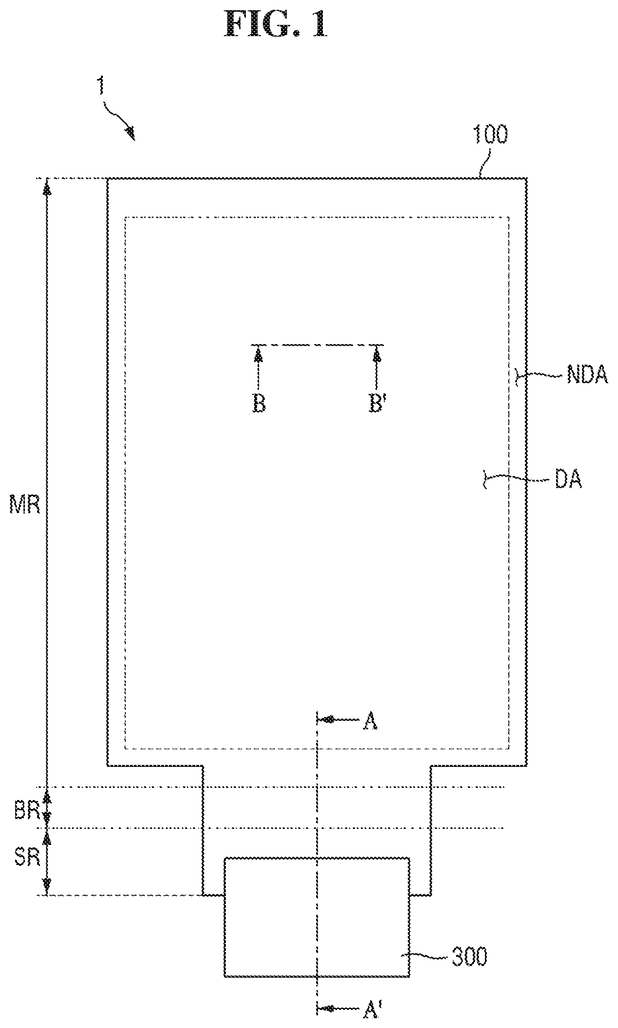
is a plan view of a display device 1 which may be manufactured by an apparatus according to an embodiment. is a cross-sectional view taken along line A-A′ of , and is a cross-sectional view taken along line B-B′ of .
Referring to , the display device 1 may be any one of various devices that displays still images or video. The display device 1 may be included, for example, in a smartphone, a mobile phone, a tablet PC, a personal digital assistant (PDA), a portable multimedia player (PMP), a television, a game machine, a wrist watch type electronic device, a head mounted display, a monitor of a personal computer, a laptop computer, a car navigation, a car dashboard, a digital camera, a camcorder, an external billboard, an electronic sign, various medical devices, various inspection devices, various home appliances such as a refrigerator or a washing machine including a display unit, Internet of Things devices, or the like. However, the present disclosure is not limited thereto.
The display device 1 may be manufactured, for example, by various embodiments of a manufacturing apparatus (e.g., 10 in ) and method as described herein. However, display device 1 may also be manufactured by apparatuses and methods which are different from the embodiments described herein.
Referring to , the display device 1 may include a display panel 100 having a predetermined shape, e.g., a substantially rectangular shape when viewed on a plane. Corners of the display panel 100 may have one or more predetermined shapes, e.g., a pointed shape (e.g., in which adjacent sides are orthogonal to each other or jointed at another angle) on a plane. In one embodiment, one or more corners may be rounded. In one embodiment, the display panel 100 may have a shape corresponding to an L-shape when viewed on a plane. This shape may correspond, for example, to corners adjacent to a portion to which a printed circuit board (e.g., 300 ) is connected. However, other shapes are possible.
The display panel 100 is flexible and can be bent and, for example, may be an organic light emitting display panel. The display panel 100 may be a different type of display panel in another embodiment. Examples include a liquid crystal display (LCD), a quantum dot organic light emitting display panel (QD-OLED), a quantum dot liquid crystal display (QD-LCD), a quantum nano light emitting display panel (Nano NED), or a Micro LED.
The display panel 100 includes a display area DA and a non-display area NDA disposed around the display area DA. The display area DA includes a plurality of pixels to display still images or video and may have a predetermined shape, e.g., substantially rectangular shape, circular shape, elliptical shape or another shape when viewed on a plane.
The non-display area NDA may not display an image or a video and, for example, may correspond to a remaining area of the display device 1 , except for the display area DA. The non-display area NDA may surround at least a portion of the display area DA. For example, as illustrated in , the non-display area NDA may be in a substantially band shape surrounding the display area DA on a plane. However, the present disclosure is not limited thereto, and the non-display area NDA may be adjacent to only both short sides or both long sides of the display area DA. When the display area is not rectangular, the non-display area NDA may be completely or partially surround one or more sides of the display area DA.
The display panel 100 may include a main region MR, a bending region BR, and a sub region SR. The main region MR may be a flat region including the display area DA and, for example, may have a substantially rectangular or other shape when viewed on a plane. The main region MR may include a portion of the non-display area NDA.
The bending region BR and the sub region SR may be in the non-display area NDA and may be on one or more sides of the main region MR. In one embodiment one side of the bending region BR may be connected to the one side of the main region MR. As illustrated in , the one side of the main region MR may be a lower side of the main region MR in a plan view. However, the present disclosure is not limited thereto.
The sub region SR may be on the other (or another) side of the bending region BR. One side of the sub region SR may be connected to the other (or another) side of the bending region BR. In one embodiment, the sub region SR may be connected to the main region MR by the bending region BR. As illustrated in , the bending region BR may be bent so that the sub region SR overlaps the main region MR in a thickness direction. In this case, printed circuit board 300 , which is connected to the sub region SR, may also overlap the main region MR in the thickness direction.
The display device 1 may further include an adhesive member CM between the main region MR and the sub region SR. The main region MR and the sub region SR may be attached to each other by the adhesive member CM.
Referring to , the display panel 100 includes a substrate SUB, a plurality of conductive layers 120 , 130 , 140 , and 150 on the substrate SUB, a plurality of insulating layers 111 , 112 , 113 , VIA 1 , and VIA 2 which insulate the conductive layers, and a light emitting layer EL. The substrate SUB may be over, on, or adjacent to the display area DA and the non-display area NDA. The substrate SUB may be a flexible substrate SUB including a flexible material, e.g., ductile glass, polyimide, and/or another material.
A buffer layer BFF may be on the substrate SUB to prevent moisture and oxygen from penetrating from the substrate SUB through other layers. The buffer layer BFF may include, for example, one of a silicon nitride (SiN x ) film, silicon oxide (SiO 2 ) film, or silicon oxynitride (SiO x Ny) film.
The semiconductor layer 105 may be on the buffer layer BFF and, for example, may correspond to a channel of a thin film transistor. The semiconductor layer 105 may be in pixels of the display area DA, and in some cases may also be in the non-display area NDA. The semiconductor layer 105 may include, for example, polycrystalline silicon.
A first insulating layer 111 may be on the semiconductor layer 105 and on or over all or a portion of the substrate SUB. The first insulating layer 111 may serve, for example, as a gate insulating film having a gate insulating function. The first insulating layer 111 may include a silicon compound, a metal oxide, or another material. For example, the first insulating layer 111 may include silicon oxide, silicon nitride, silicon oxynitride, aluminum oxide, tantalum oxide, hafnium oxide, zirconium oxide, or titanium oxide used alone or in combination with each other or another material.
A first conductive layer 120 may be on the first insulating layer 111 and may include a gate electrode GE of a thin film transistor TFT and a first electrode CE 1 of a storage capacitor. The first conductive layer 120 may include, for example, at least one of molybdenum (Mo), aluminum (Al), platinum (Pt), palladium (Pd), silver (Ag), magnesium (Mg), gold (Au), nickel (Ni), neodymium (Nd), iridium (Ir), chromium (Cr), calcium (Ca), titanium (Ti), tantalum (Ta), tungsten (W), or copper (Cu). The first conductive layer 120 may be, for example, a single film or a stacked film formed of one or more of the aforementioned materials.
A second insulating layer 112 a may be on the first conductive layer 120 and may insulate the first conductive layer 120 and the second conductive layer 130 . The second insulating layer 112 a may include materials similar to those used, for example, for the first insulating layer 111 .
The second conductive layer 130 may be on the second insulating layer 112 a and may include a second electrode CE 2 of the storage capacitor. The second conductive layer 130 may include materials similar to those of the first conductive layer 120 . The storage capacitor may be formed by the first electrode CE 1 and the second electrode CE 2 , with the second insulating layer 112 a therebetween.
A third insulating layer 113 may be on the second conductive layer 130 and may include at least one of the materials of the first insulating layer 111 , as described above. In one or more embodiments, the third insulating layer 113 may include an organic insulating material, which, for example, may correspond to one of those used for a first via layer VIA 1 described below.
A third conductive layer 140 may be on the third insulating layer 113 and may include a source electrode SE, a drain electrode DE, a high potential voltage electrode ELVDDE, and a signal line PAD. The third conductive layer 140 may include at least one of molybdenum (Mo), aluminum (Al), platinum (Pt), palladium (Pd), silver (Ag), magnesium (Mg), gold (Au), nickel (Ni), neodymium (Nd), iridium (Ir), chromium (Cr), calcium (Ca), titanium (Ti), tantalum (Ta), tungsten (W), or copper (Cu). In one embodiment, the third conductive layer 140 may be a single film formed of one or more of the aforementioned metals. In one embodiment, the third conductive layer 140 may include a stacked film. For example, the third conductive layer 140 may be formed in a stacked structure, such as but not limited to Ti/Al/Ti, Mo/Al/Mo, Mo/AlGe/Mo, and Ti/Cu. In one embodiment, the third conductive layer 140 may include Ti/Al/Ti.
The first via layer VIA 1 may be on the third conductive layer 140 and may include an organic insulating material. The organic insulating material may include at least one of an acrylic resin, an epoxy resin, a phenolic resin, a polyimide resin, a polyimide resin, an unsaturated polyester resin, a poly phenylene ether resin, a polyphenylene sulfide resin, or benzocyclobutene (BCB).
A fourth conductive layer 150 may be on the first via layer VIA 1 and may include a data line DL, a connection electrode CNE, and a high potential voltage line ELVDDL. The data line DL may be electrically connected to the source electrode SE of the thin film transistor TFT through a contact hole penetrating the first via layer VIAL The connection electrode CNE may be electrically connected to the drain electrode DE of the thin film transistor TFT through a contact hole penetrating the first via layer VIA 1 . The high potential voltage line ELVDDL may be electrically connected to the high potential voltage electrode ELVDDE through a contact hole penetrating the first via layer VIAL The fourth conductive layer 150 may include a material corresponding to those of the third conductive layer 140 .
A second via layer VIA 2 may be on the fourth conductive layer 150 and may include at least one of the materials of the first via layer VIA 1 described above.
An anode ANO may be on the second via layer VIA 2 and electrically connected to the connection electrode CNE through a contact hole penetrating the second via layer VIA 2 .
A bank layer BANK may be on the anode ANO and may include a contact hole which exposes the anode ANO. The bank layer BANK may include an organic insulating material or an inorganic insulating material. For example, the bank layer BANK may be formed to include at least one of a photoresist, a polyimide resin, an acrylic resin, a silicone compound, or a polyacrylic resin.
The light emitting layer EL may be on an upper surface of the anode ANO and in an opening OP of the bank layer BANK. A cathode CAT is on the light emitting layer EL and the bank layer BANK and may be a common electrode disposed over a plurality of pixels.
A thin film encapsulation layer TFE may be on the cathode CAT and may cover an organic light emitting device OLED. In one embodiment, the thin film encapsulation layer TFE may be a stacked film in which an inorganic film and an organic film are alternately stacked. For example, the thin film encapsulation layer TFE may include a first encapsulation inorganic film 171 , an encapsulation organic film 172 , and a second encapsulation inorganic film 173 which are sequentially stacked.
The display panel 100 may include a panel lower sheet CPNL on a lower surface of the substrate SUB. For example, the panel lower sheet CPNL may include at least one functional layer such as a digitizer, a heat dissipation member, a shield member, and a buffer member.
Referring again to , the display device 1 may further include the printed circuit board 300 . One side of the printed circuit board 300 may be attached to the other side of the sub region SR. The printed circuit board 300 may be a flexible circuit board. The display device 1 may further include a main circuit board attached to the other side of the printed circuit board 300 .
The display device 1 may further include a driving member 200 which drives the plurality of pixels in the display area DA. The driving member 200 may include a display driving integrated circuit. The driving member 200 may be mounted on the sub region SR between the bending region BR of the display panel 100 and the flexible circuit board on a plan view or may be mounted on the printed circuit board 300 . The driving member 200 may be attached to the display panel 100 in a chip on plastic (COP) method, a chip on glass (COG) method, or a chip on film (COF) method.
As described above, the bending region BR of the display panel 100 may be bent so that the sub region SR overlaps the main region MR in the thickness direction. This bending may be performed by the display device manufacturing apparatus (e.g., 10 in ) and the display device manufacturing method to be described later.
is a perspective view of an embodiment of an apparatus 10 for manufacturing a display device. is a perspective view of embodiment of the apparatus 10 in a state in which a target board is mounted. is a cross-sectional view taken along line C-C′ of . is a perspective view of an embodiment which includes a rotating member (or rotator), a first arm module, and a second arm module.
In these figures, a first direction X, a second direction Y, and a third direction Z intersect in different directions. In one embodiment, the first direction X, the second direction Y, and the third direction Z may intersect each other perpendicularly. The first direction X may be a horizontal direction, the second direction Y may be a vertical direction, and the third direction Z may be a thickness direction. The first direction X, the second direction Y, and/or the third direction Z may include two or more directions. For example, the third direction Z may include an upward direction toward an upper side of the drawing and a downward direction toward a lower side of the drawing. In this case, one surface of a member facing upward may be referred to as an upper surface, and the other surface of the member facing downward may be referred to as a lower surface. However, the directions are illustrative and relative, and are not limited to those mentioned above.
Referring to to 6 , the apparatus 10 of manufacturing a display device may include a first working table PS 1 , a second working table PS 2 , a rotating member (or rotator) RM, a first arm module AR 1 , and a second arm module AR 2 . Each of the first working table PS 1 and the second working table PS 2 may have a predetermined shape, e.g., an approximately rectangular shape including short sides in the first direction X and long sides in the second direction Y on a plane. The tables may have a different shape in another embodiment.
The first working table PS 1 and the second working table PS 2 may be arranged in the first direction X. The first working table PS 1 and the second working table PS 2 may be spaced apart from each other in the first direction X on a first stage ST 1 to be described later. The first working table PS 1 and the second working table PS 2 may be connected to each other by the first stage ST 1 . In one embodiment, the first working table PS 1 and the second working table PS 2 may be disposed so that respective long sides thereof face each other. However, the present disclosure is not limited thereto.
Each of the first working table PS 1 and the second working table PS 2 may be configured to be movable and/or rotatable in at least one direction. In one embodiment, each of the first working table PS 1 and the second working table PS 2 is movable in the first direction X, the second direction Y, and the third direction Z and rotatable about a rotation axis extending in the third direction Z. However, the present disclosure is not limited thereto.
Each of the first working table PS 1 and the second working table PS 2 may include at least one servo motor which provides power for movement and/or rotation thereof. Each of the first working table PS 1 and the second working table PS 2 may include a linear stage and/or a UVW stage. In one embodiment, the first working table PS 1 and the second working table PS 2 may be provided as separate stages, which may have a size smaller than that of the first stage ST 1 and may be disposed above the first stage ST 1 so that the target board is directly mounted.
The display device 1 may further include the first stage ST 1 which supports the first working table PS 1 and the second working table PS 2 . The first stage ST 1 may be disposed below the first working table PS 1 and the second working table PS 2 . The first working table PS 1 and the second working table PS 2 may be mounted on the first stage ST 1 . The first stage ST 1 may be connected to the first working table PS 1 and the second working table PS 2 and may move and/or rotate the first working table PS 1 and the second working table PS 2 in at least one direction. As described later, the first stage ST 1 may integrally move and/or rotate the first working table PS 1 and the second working table PS 2 .
In one embodiment, the first stage ST 1 may move the first working table PS 1 and the second working table PS 2 in at least one direction of the first direction X, the second direction Y, and the third direction Z and rotate the first working table PS 1 and the second working table PS 2 about an arbitrary axis extending in the third direction Z. However, the present disclosure is not limited thereto. A driver which provides power for moving and/or rotating the first stage ST 1 may be mounted on the first stage ST 1 . The first stage ST 1 may include a linear stage and/or a UVW stage.
The rotating member (or rotator) RM may be on one side of the first working table PS 1 and the second working table PS 2 and may extend in the first direction X. The rotating member RM may be disposed along one short side of the first working table PS 1 in the first direction X and one short side of the second working table PS 2 in the first direction X. The length of the rotating member RM in the first direction X may be greater than the sum of a length of the one short side of the first working table PS 1 and a length of the one short side of the second working table PS 2 . The rotating member RM may be configured to be rotatable about an arbitrary axis in the second direction Y.
The display device manufacturing apparatus 10 may further include a rotating member support portion RT_SP, a rotation driver RM_D, and a second stage ST 2 . The rotating member support portion RT_SP may support the rotating member RM so that the rotating member RM is positioned at a predetermined position with respect to the first working table PS 1 and the second working table PS 2 . The rotating member support portion RT_SP may be connected to respective sides of the rotating member RM. Each of respective sides of the rotating member RM may be rotatably connected to the rotating member support portion RT_SP. The rotating member support portion RT_SP may connect the rotating member RM and the second stage ST 2 . In one embodiment, the rotating member support portion RT_SP may be a frame having a “U” shape surrounding a portion of the rotating member RM, but may have a different shape in another embodiment.
The rotation driver RM_D may be connected to at least one of two sides of the rotating member RM. The rotation driver RM_D may provide power for rotation of the rotating member RM.
The first arm module AR 1 and the second arm module AR 2 may be connected to the rotating member RM. While the first arm module AR 1 and the second arm module AR 2 may be connected to a middle of the rotating member RM extending in the first direction X, the first arm module AR 1 and the second arm module AR 2 may be disposed at positions corresponding to the first working table PS 1 and the second working table PS 2 , respectively.
As illustrated in , while the first arm module AR 1 and the second arm module AR 2 are arranged in the first direction X, the first arm module AR 1 may be between the rotating member RM and the first working table PS 1 and the second arm module AR 2 may be between the rotating member RM and the second working table PS 2 . In this case, the first working table PS 1 and the first arm module AR 1 may be arranged in the second direction Y, and the second working table PS 2 and the second arm module AR 2 may also be arranged in the second direction Y, on a plane. When the rotating member RM is rotated, the first arm module AR 1 and second arm module AR 2 may rotate together with rotating member RM.
The display device manufacturing apparatus 10 may further include the second stage ST 2 , which may be connected to the rotating member support portion RT_SP and which may move and/or rotate the rotating member support portion RT_SP in at least one direction. The second stage ST 2 may move and/or rotate the rotating member support portion RT_SP so that the rotating member RM and the rotating member support portion RT_SP integrally move and/or rotate.
In one embodiment, the second stage ST 2 may move the rotating member support part RT_SP in the first direction X, the second direction Y, and the third direction Z, and rotate the rotating member support portion RT_SP about an arbitrary axis extending in the third direction Z. However, the present disclosure is not limited thereto.
A driver which provides power for moving and/or rotating the second stage ST 2 may be mounted on the second stage ST 2 . The second stage ST 2 may include a linear stage and/or a UVW stage.
As illustrated in , a first target board T 1 and a second target board T 2 may be mounted on the display device manufacturing apparatus 10 . The first target board T 1 may include a first base board T 11 and a first flexible circuit board T 12 connected to the first base board T 11 . The second target board T 2 may include a second base board T 21 and a second flexible circuit board T 22 connected to the second base board T 21 .
Each of the first base board T 11 and the second base board T 21 may be the flexible display panel 100 or the substrate SUB of flexible display panel 100 , and the first flexible circuit board T 12 and the second flexible circuit board T 22 may be the printed circuit board 300 connected to the flexible display panel 100 . For example, the first base board T 11 and the second base board T 21 may be the board of to 3 , and the first flexible circuit board T 12 and the second flexible circuit board T 22 may be the printed circuit board 300 of to 3 . In this case, the first target board T 1 and the second target board T 2 may be inverted and mounted so that the display area DA faces the first working table PS 1 or the second working table PS 2 . However, the first target board T 1 and the second target board T 2 are not limited to the display panel 100 and the printed circuit board 300 of to 3 .
The first base board T 11 and the second base board T 21 may be mounted on the first working table PS 1 and the second working table PS 2 , respectively. For example, the first working table PS 1 and the second working table PS 2 may include a position fixing unit such as an electrostatic chuck, an adhesive chuck, and a vacuum chuck, and thus, a relative position of the first base board T 11 or the second base board T 21 with respect to the first working table PS 1 or the second working table PS 2 may be fixed by the position fixing unit.
In one embodiment, as illustrated in , the first working table PS 1 may include at least one air hole AH_PS 1 in which a negative pressure is provided, one-side opening of the air hole AH_PS 1 may be disposed on the upper surface of the first working table PS 1 , and thus the first base board T 11 may be adsorbed and fixed to the first working table PS 1 . The second working table PS 2 may also include an air hole substantially the same as or similar to the air hole AH_PS 1 of the first working table PS 1 .
As illustrated in , the first flexible circuit board T 12 may be disposed on the first arm module AR 1 and the rotating member RM, and the second flexible circuit board T 22 may be disposed on the second arm module AR 2 and the rotating member RM. The first flexible circuit board T 12 may overlap a first adsorber AS 1 and a first pusher PSH 1 in the thickness direction, and the second flexible circuit board T 22 may overlap a second adsorber AS 2 and a second pusher PSH 2 in the thickness direction.
The first arm module AR 1 , the second arm module AR 2 , and/or a module mounter MM are spaced apart from the printed circuit board 300 , and then may come into close contact (e.g., to within a predetermined distance) with the first flexible circuit board T 12 or the second flexible circuit board T 22 after the alignment of the first target board T 1 and the second target board T 2 is completed. However, the present disclosure is not limited thereto. For example, the first flexible circuit board T 12 and the second flexible circuit board T 22 may be disposed only on the first arm module AR 1 and the second arm module AR 2 , respectively, and the first arm module AR 1 and the second arm module AR 2 may be in close contact (e.g., to within a predetermined distance) with the first flexible circuit board T 12 or the second flexible circuit board T 22 even before the first target board T 1 and the second target board T 2 are aligned.
One side of the first flexible circuit board T 12 may be connected to one side of the first base board T 11 between the first working table PS 1 and the rotating member RM. The other side of the first flexible circuit board T 12 may be disposed on the rotating member RM. One side and the other side of the second flexible circuit board T 22 may also be disposed in a manner substantially the same as or similar to the first flexible circuit board T 12 .
As illustrated in , the first working table PS 1 and the second working table PS 2 may perform an alignment operation of moving and/or rotating in at least one direction. For example, the alignment operation may be performed before or after the first target board T 1 and the second target board T 2 are mounted and/or before and after the first target board T 1 and the second target board T 2 are bent. By the alignment operation, the first target board T 1 and the second target board T 2 may be aligned to positions suitable for bending and/or pressing. The display device manufacturing apparatus 10 may further include a controller which controls the alignment operation.
The display device manufacturing apparatus 10 may further include at least one detector VC disposed above the first working table PS 1 and/or the second working table PS 2 . The alignment operation may be performed based on at least position information of the first target board T 1 and the second target board T 2 obtained by the detector VC.
The first working table PS 1 and the second working table PS 2 may perform the alignment operation independently of each other. For example, the first working table PS 1 and the second working table PS 2 may individually perform the alignment operation. When the alignment operation is performed, the movement direction and/or rotation direction of the first working table PS 1 may be different from the movement direction and/or rotation direction of the second working table PS 2 . In this case, the movement distance and/or rotation angle of the first working table PS 1 may be substantially the same as or different from a movement distance and/or a rotation angle of the second working table PS 2 . In one embodiment, when the alignment operation is performed, the movement direction and/or the rotation direction of the first working table PS 1 may be substantially the same as the movement direction and/or the rotation direction of the second working table PS 2 . The movement distance and/or the rotation angle of the first working table PS 1 may be different from the movement distance and/or the rotation angle of the second working table PS 2 .
For example, the first working table PS 1 may move in the first direction X based on the position information of the first target board T 1 , and the second working table PS 2 may move in the second direction Y different from the first direction X based on the position information of the second target board T 2 . In one example, the first working table PS 1 may rotate clockwise about an axis of the third direction Z based on the position information of the first target board T 1 , and the second working table PS 2 may rotate counterclockwise about an axis of the third direction Z based on the position information of the second target board T 2 . The movement and rotation as described above may be performed at substantially the same time. However, the present disclosure is not limited thereto.
Before and after the first target board T 1 and the second target board T 2 are mounted and/or before and after the first target board T 1 and the second target board T 2 are bent, the first stage ST 1 and/or the second stage ST 2 may perform an alignment operation of moving and/or rotating in at least one direction. Similar to the first working table PS 1 and the second working table PS 2 , the movement and/or rotation of the first stage ST 1 and the second stage ST 2 may be performed independently of each other.
In one embodiment, only the first working table PS 1 and the second working table PS 2 may perform the alignment operation before and after the first target board T 1 and the second target board T 2 are mounted and/or before and after the first target board T 1 and the second target board T 2 are bent. However, the present disclosure is not limited thereto. The alignment operation of the first stage ST 1 or the second stage ST 2 may be performed at substantially the same time as the alignment operation of the first working table PS 1 or the second working table PS 2 , and only the alignment operation of the first stage ST 1 and/or the second stage ST 2 may be performed.
Referring further to , the rotating member RM may include a first rotation plate RP 1 , a second rotation plate RP 2 , a connection frame BF, and the module mounter MM. The first rotation plate RP 1 and the second rotation plate RP 2 may be arranged in the first direction X. The first arm module AR 1 and the second arm module AR 2 may be between the first rotation plate RP 1 and the second rotation plate RP 2 . Each of the first rotation plate RP 1 and the second rotation plate RP 2 may be formed, for example, of a plate-shaped member and may have a cross section of an approximately circular shape, water droplet shape, or elliptical shape. However, the present disclosure is not limited thereto.
The connection frame BF may be constituted by a rod-shaped member extending in the first direction X. The connection frame BF may have one side connected to the first rotation plate RP 1 and another side connected to the second rotation plate.
The module mounter MM may be between the first rotation plate RP 1 and the second rotation plate RP 2 . The module mounter MM may be on one side of the connection frame BF facing the first working table PS 1 and the second working table PS 2 . The module mounter MM may extend along one side of the connection frame BF extending in the first direction X. The module mounter MM may mount the first arm module AR 1 and the second arm module AR 2 .
The first arm module AR 1 may include a first adsorber AS 1 , and the second arm module AR 2 may include a second adsorber AS 2 . The first arm module AR 1 may further include a first pusher PSH 1 , and the second arm module AR 2 may further include a second pusher PSH 2 . The first adsorber AS 1 and the second adsorber AS 2 may be spaced apart from each other on the module mounter MM and may be arranged in the first direction X. As illustrated in , the first flexible circuit board T 12 and the second flexible circuit board T 22 may be mounted on the first adsorber AS 1 and the second adsorber AS 2 , respectively.
The first adsorber AS 1 and the second adsorber AS 2 may include a position fixing unit such as an electrostatic chuck, an adhesive chuck, and a vacuum chuck. Thus, a relative position of the first flexible circuit board T 12 or the second flexible circuit board T 22 with respect to the first adsorber AS 1 or the second adsorber AS 2 may be fixed by the position fixing unit. In one embodiment, positioning of the first flexible circuit board T 12 and the second flexible circuit board T 22 by the first adsorber AS 1 and the second adsorber AS 2 may be performed after the first target board T 1 and the second target board T 2 are aligned.
The first adsorber AS 1 and the second adsorber AS 2 may be controlled at substantially the same time or individually. For example, depending on process conditions, the first adsorber AS 1 and the second adsorber AS 2 may be driven interdependently or independently of each other. For example, the first adsorber AS 1 and the second adsorber AS 2 may adsorb the first flexible circuit board T 12 or the second flexible circuit board T 22 at substantially the same time, or may adsorb the first flexible circuit board T 12 or the second flexible circuit board T 22 with a time difference. In one example, an adsorption force of the first adsorber AS 1 and an adsorption force of the second adsorber AS 2 may be adjusted equally or differently from each other.
In one embodiment, as illustrated in , the first adsorber AS 1 may include an air hole AH_AS 1 for adsorbing the first flexible circuit board T 12 mounted on the first adsorber AS 1 . The second adsorber AS 2 may also include an air hole substantially the same as or similar to the air hole AH_AS 1 of the first adsorber AS 1 .
The first pusher PSH 1 and the second pusher PSH 2 may be on one side of the module mounter MM and/or the rotating member RM facing the first working table PS 1 and the second working table PS 2 . The first pusher PSH 1 and the second pusher PSH 2 may be connected to the rotating member RM by the module mounter MM.
As illustrated in , the first pusher PSH 1 may be between the first adsorber AS 1 and the first working table PS 1 , and the second pusher PSH 2 may be between the second adsorber AS 2 and the second working table PS 2 . The first pusher PSH 1 and the first adsorber AS 1 may be arranged in the second direction Y, and the second pusher PSH 2 and the second adsorber AS 2 may be arranged in the second direction Y.
In one embodiment, as illustrated in , the first pusher PSH 1 and the second pusher PSH 2 may be configured to be movable in the third direction Z. For example, the third direction Z may include a vertical direction. In one example, the third direction Z may include one direction and the other direction opposite to the one direction. The one direction and the other side direction may be closer to the first flexible circuit board T 12 or the second flexible circuit board T 22 and away from the first flexible circuit board T 12 or the second flexible circuit board T 22 , respectively.
When the first base board T 11 and the second base board T 21 are bent, the first pusher PSH 1 and the second pusher PSH 2 press the first flexible circuit board T 12 and the second flexible circuit board T 22 , respectively, and thus the first target board T 1 and the second target board T 2 can be prevented from being warped. The first pusher PSH 1 and the second pusher PSH 2 may include at least one air hole for adsorbing the first flexible circuit board T 12 or the second flexible circuit board T 22 .
As illustrated in , before rotation of the rotating member RM for bending the first target board Ti, the first working table PS 1 , the first pusher PSH 1 and the first adsorber AS 1 may be sequentially arranged in the second direction Y. The second working table PS 2 , the second pusher PSH 2 , and the second adsorber AS 2 may also be sequentially arranged in the second direction Y. In this case, the first adsorber AS 1 , the module mounter MM, and the first pusher PSH 1 may be between the connection frame BF and the first working table PS 1 , and the second adsorber AS 2 , the module mounter MM, and the second pusher PSH 2 may be between the connection frame BF and the second working table PS 2 .
The first working table PS 1 may support a lower surface of the first base board T 11 , and the connection frame BF, the first arm module AR 1 , and the module mounter MM may support a lower surface of the first flexible circuit board T 12 . The second base board T 21 and the second flexible circuit board T 22 may also be supported by the second working table PS 2 , the connection frame BF, the second arm module AR 2 , and the module mounter MM in a manner substantially the same as or similar to the first base board T 11 and the first flexible circuit board T 12 .
Before the first target board T 1 and the second target board T 2 are bent, the first pusher PSH 1 and the second pusher PSH 2 may be spaced apart from the first target board T 1 or the second target board T 2 . However, the present disclosure is not limited thereto.
is a perspective view of an embodiment of an apparatus for manufacturing a display device in a state in which the target board is bent. is a cross-sectional view taken along line D-D′ of .
Referring to to 9 , the first target board T 1 and the second target board T 2 may be bent by the rotation of the rotating member RM. Bending of the first target board T 1 and the second target board T 2 may be performed after the first target board T 1 and the second target board T 2 are seated and/or aligned.
Referring to , as described above, the rotating member RM may rotate about an arbitrary rotation axis extending in the first direction X. The rotation axis may pass through the rotating member RM or may be provided outside the rotating member RM. The rotation axis may be an actual shaft provided by a shaft or the like, or may be a virtual axis. When the rotating member RM rotates, the first arm module AR 1 and the second arm module AR 2 connected to the rotating member RM may also rotate together. Accordingly, when the rotating member RM rotates, the first target board T 1 and the second target board T 2 may be bent at substantially the same time.
As illustrated in , the rotating member RM may rotate toward a direction in which the first target board T 1 and the second target board T 2 are mounted, for example, may rotate counterclockwise. However, the present disclosure is limited thereto.
For example, the first adsorber AS 1 adsorbs the first flexible circuit board T 12 and rotates together with the rotating member RM when the rotating member RM rotates, and thus the first base board T 11 can be bent. As illustrated in , for example, the first base board T 11 may be bent to have a “U”-shaped cross section. When the first base board T 11 is bent, the connection frame BF, the first adsorber AS 1 , and the first pusher PSH 1 may overlap the first base board T 11 in the thickness direction.
As illustrated in , when the first base board T 11 is bent, the first flexible circuit board T 12 and a portion of the first base board T 11 connected to the first flexible circuit board T 12 may overlap another portion of the first base board T 11 in the thickness direction. For example, a portion of the first base board T 11 , another portion of the first base board T 11 , and a bent portion between the portion of the first base board T 11 and another portion of the first base board T 11 may be the sub region SR, the main region MR, and the bending region BR of , respectively.
As illustrated in , the adhesive member CM may be interposed between the portion of the first base board T 11 and another portion of the first base board T 11 . Similar to the first base board T 11 , the adhesive member CM may also be between a portion of the second base board T 21 and another portion of the second base board T 21 .
Similarly, as in , the second base board T 21 of the second target board T 2 may also be bent in a manner substantially the same as or similar to the first base board T 11 by the rotations of the second adsorber AS 2 and the rotating member RM. When the second base board T 21 is bent, the second base board T 21 has a cross section having a “U” shape like the base board of , and the connection frame BF, the second adsorber AS 2 , and the second pusher PSH 2 may overlap the second base board T 21 in the thickness direction.
As described above, when the first base board T 11 and the second base board T 21 are bent, the first working table PS 1 and/or the second working table PS 2 may perform the alignment operation of moving and/or rotating in at least one direction. As described above, the alignment operation of the first working table PS 1 and the alignment operation of the second working table PS 2 may be performed independently of each other. When the first working table PS 1 and/or the second working table PS 2 performs the alignment operation, the first stage ST 1 and/or the second stage ST 2 may perform an additional alignment operation. However, the present disclosure is not limited thereto.
When the first base board T 11 and the second base board T 21 are bent, the first pusher PSH 1 and the second pusher PSH 2 may move toward the first flexible circuit board T 12 and the second flexible circuit board T 22 , respectively. For example, as illustrated in , the first pusher PSH 1 and the second pusher PSH 2 may be lowered in the third direction Z. The first pusher PSH 1 and the second pusher PSH 2 may be in close contact with the first flexible circuit board T 12 and the second flexible circuit board T 22 , respectively, to prevent the first flexible circuit board T 12 or the second flexible circuit board T 22 from being warped.
The first pusher PSH 1 and the second pusher PSH 2 may be controlled at substantially the same time or individually. For example, depending on process conditions, the first pusher PSH 1 and the second pusher PSH 2 may be driven interdependently or independently of each other. For example, the first pusher PSH 1 and the second pusher PSH 2 may move by substantially the same distance or by different distances. For another example, the first pusher PSH 1 and the second pusher PSH 2 may be moved at substantially the same time or may be moved with a time difference. Each of the first pusher PSH 1 and the second pusher PSH 2 may be implemented by a linear guide including a servo motor or a cylinder configured to be stretchable. However, the present disclosure is not limited thereto.
Referring to , when the first base board T 11 and the second base board T 21 are bent and/or aligned, a first pressing member FAM 1 and a second pressing member FAM 2 may be lowered toward the first target board T 1 and the second target board T 2 , respectively. The first pressing member FAM 1 may press a portion of the first base board T 11 to another portion of the first base board T 11 , and second pressing member FAM 2 may press a portion of the second base board T 21 to another portion of second base board T 21 .
The portion of the first base board T 11 may refer to a portion to which the first flexible circuit board T 12 is connected and a portion adjacent thereto, and the portion of the second base board T 21 may refer to a portion to which the second flexible circuit board T 22 is connected and a portion adjacent thereto.
Referring to , the portion of the first base board T 11 pressed by the first pressing member FAM 1 may overlap the adhesive member CM of the first flexible circuit board T 12 . Likewise, the portion of the second base board T 21 pressed by the second pressing member FAM 2 may overlap the adhesive member CM.
After the pressing is completed, the first pressing member FAM 1 and the second pressing member FAM 2 move away from the first target board T 1 or the second target board T 2 , and the first target board T 1 and the second target board T 2 may be unloaded from the first working table PS 1 or the second working table PS 2 . For example, through the above processes, the display device 1 may be manufactured to include display panel 100 , in which the bending region BR as illustrated in is formed with the printed circuit board 300 connected to the display panel 100 .
In to 9 , two target boards, two working tables, and two arm modules are illustrated. However, the number of target boards, the number of working tables, and the number of arm modules are not limited thereto. The manufacturing apparatus 10 of the display device may include three or more working tables and three or more arm modules.
Only one first target board T 1 may be mounted on the first working table PS 1 and bent, or only one second target board T 2 may be mounted on the second working table PS 2 and bent. In this case, only one of the first arm module AR 1 and the second arm module AR 2 may be operated. For example, when only the first target board T 1 is mounted, only the first adsorber AS 1 and the first pusher PSH 1 may be operated. When only the second target board T 2 is mounted, only the second adsorber AS 2 and the second pusher PSH 2 may be operated.
is a perspective view of an embodiment of an apparatus for manufacturing a display device. is a perspective view of the apparatus of in a state in which a target board is bent.
Referring to , unlike the embodiment of to 9 , only one third target board T 3 may be mounted on the first working table PS 1 and the second working table PS 2 . The third target board T 3 may have a larger size than the first target board T 1 and the second target board T 2 of to 9 . The third target board T 3 may be bent and pressed in a manner substantially the same as or similar to the first target board T 1 and/or the second target board T 2 of to 9 .
The third target board T 3 may include a third base board T 31 and a third flexible circuit board T 32 . For example, the third base board T 31 and the third flexible circuit board T 32 may be the display panel 100 and the printed circuit board 300 of to 3 , respectively. However, the present disclosure is not limited thereto.
As illustrated in , the third base board T 31 may be disposed over the first working table PS 1 and the second working table PS 2 . The third flexible circuit board T 32 may be disposed on the first arm module AR 1 and the second arm module AR 2 .
Referring to , the third flexible circuit board T 32 may be adsorbed by the first adsorber AS 1 and the second adsorber AS 2 . When the rotating member RM rotates, the third base board T 31 may be bent to have a “U”-shaped cross section, similar to the first base board T 11 illustrated in .
When the third base board T 31 is bent, similar to the embodiment of , the first pusher PSH 1 and the second pusher PSH 2 may be lowered toward the third flexible circuit board T 32 . The first pusher PSH 1 and the second pusher PSH 2 may be in close contact (e.g., to within a predetermined distance) with the third flexible circuit board T 32 to prevent the third flexible circuit board T 32 from being warped.
When the third base board T 31 is bent, similar to the embodiment of , a pressing member FAM is lowered toward the third target board T 3 , and thus a portion of the third target board T 3 can be pressed to another portion of the third target board T 3 . Although one pressing member FAM is illustrated in , the number of pressing members FAM is not limited thereto.
As described above, the first adsorber AS 1 and the second adsorber AS 2 may be controlled at substantially the same time or individually. Likewise, the first pusher PSH 1 and the second pusher PSH 2 may be controlled at substantially the same time individually.
Before and after the third target board T 3 is mounted and/or the third target board T 3 (third base board T 31 ) is bent, the first stage ST 1 and/or the second stage ST 2 may perform an alignment operation of moving and/or rotating in at least one direction. Accordingly, the position of the third target board T 3 may be appropriately adjusted to a position suitable for bending and/or bonding. During the alignment operation of the first stage ST 1 , the first working table PS 1 and the second working table PS 2 connected to the first stage ST 1 may be moved and/or rotated integrally.
For example, in a first mode in which the first target board T 1 and the second target board T 2 are mounted on the first working table PS 1 and the second working table PS 2 , respectively, when the first target board T 1 and the second target board T 2 are aligned, the first working table PS 1 and/or the second working table PS 2 may move and/or rotate. Moreover, in a second mode in which the third target board T 3 is mounted over the first working table PS 1 and the second working table PS 2 , when the first target board T 1 and the second target board T 2 are aligned, the first stage ST 1 and/or the second stage ST 2 may move and/or rotate. The embodiment of may be substantially the same as or similar to the embodiment of to 9 , except for the third target board T 3 .
is a flowchart illustrating an embodiment of a method for manufacturing a display device. For illustration purposes, the display device is described as corresponding to display device 1 of to 3 , and the method may be performed by the display device manufacturing apparatuses 10 and 10 a of to 11 . However, the display device and manufacturing apparatus may be different than those indicated above in other embodiments.
Referring to , the method may include an operation of mounting at least one target board on a plurality of working tables PS 1 and PS 2 ( 1210 ), an operation of adsorbing the target board using a plurality of adsorbers AS 1 and AS 1 ( 1220 ), and an operation of bending the target board by rotating a rotating member RM connected to the plurality of adsorbers AS 1 and AS 1 ( 1230 ). The at least one target board may be at least one of the first target board Ti, the second target board T 2 , and the third target board T 3 of to 11 .
At 1210 , the operation of mounting at least one target board on the plurality of working tables PS 1 and PS 2 may include an operation of mounting one target board over the plurality of working tables PS 1 and PS 2 . The method may further include an operation of aligning the target board, which may include at least one of an operation of individually moving the plurality of working tables PS 1 and PS 2 or an operation of individually rotating the plurality of working tables PS 1 and PS 2 . The display device manufacturing method is not limited to the above example, and at least some of the operations may be omitted, or at least one other operation may be further included with reference to other descriptions of the present specification.
Referring to , the operation of mounting at least one target board on the plurality of working tables PS 1 and PS 2 may include an operation of mounting a plurality of target boards for each of the plurality of working tables PS 1 and PS 2 . For example, first, the first target board T 1 and the second target board T 2 may be prepared. For example, the first target board T 1 and the second target board T 2 may be transferred from the outside by a transfer unit such as a transfer robot. As described above, the transferred first target board T 1 and second target board T 2 may be mounted on the first working table PS 1 and the second working table PS 2 , respectively.
Referring to , the display device manufacturing method may further include an operation of aligning the target board, and the operation of aligning the target board may include at least one of an operation of individually moving the plurality of working tables PS 1 and PS 2 or an operation of individually rotating the plurality of working tables PS 1 and PS 2 . For example, after the mounting of the first target board T 1 and the second target board T 2 is completed, the first working table PS 1 and the second working table PS 2 may perform the alignment operation. Accordingly, the first target board T 1 and the second target board T 2 may be aligned to appropriate positions for bending.
After alignment of the first target board T 1 and second target board T 2 is completed, the first arm module AR 1 may adsorb the first flexible circuit board T 12 , and the second arm module AR 2 may adsorb the second flexible circuit board T 22 . In one embodiment, when the first target board T 1 and the second target board T 2 are mounted, the first arm module AR 1 and the second arm module AR 2 may move to be spaced apart from the first flexible circuit board T 12 or the second flexible circuit board T 22 .
Then, when the first flexible circuit board T 12 or the second flexible circuit board T 22 is adsorbed at 1220 , the first arm module AR 1 and the second arm module AR 2 may move toward the first flexible circuit board T 12 or the second flexible circuit board T 22 and come into close proximity with the first flexible circuit board T 12 or the second flexible circuit board T 22 . However, the present disclosure is not limited thereto.
Referring to , the operation of bending the target board by rotating the rotating member RM connected to the plurality of adsorbers AS 1 and AS 1 at 1230 may include an operation of bending the plurality of target boards at substantially the same time. For example, after alignment and adsorption of the first target board T 1 and the second target board T 2 are completed, the rotating member RM may rotate so that the first target board T 1 and the second target board T 2 are bent at 1230 .
After the first target board T 1 and the second target board T 2 are bent, the first working table PS 1 and the second working table PS 2 may perform the alignment operation again. Accordingly, the first target board T 1 and the second target board T 2 may be aligned to appropriate positions for pressing.
After the alignment of the first target board T 1 and the second target board T 2 is completed, the first pressing member FAM 1 and the second pressing member FAM 2 may be respectively lowered toward the first target board T 1 and the second target board T 2 to press the first target board T 1 and the second target board T 2 .
After the pressing of the first target board T 1 and the second target board T 2 is completed, the first pressing member FAM 1 and the second pressing member FAM 2 may be raised, and the first target board T 1 and the second target board T 2 may be unloaded from the first working table PS 1 and the second working table PS 2 , respectively.
Referring to , the operation of mounting at least one target board on the plurality of working tables PS 1 and PS 2 may include an operation of mounting one target board over the plurality of working tables PS 1 and PS 2 . For example, only one third target board T 3 may be mounted on the first working table PS 1 and the second working table PS 2 . As described above, the third target board T 3 may be bent and pressed in a manner substantially the same as or similar to the first target board T 1 and the second target board T 2 by rotation of the rotating member RM.
However, when the third target board T 3 is aligned, the first working table PS 1 and the second working table PS 2 may not perform individual alignment operations, and the first stage ST 1 may perform the alignment operation so that the first working table PS 1 and the second working table PS 2 , and the third target board T 3 disposed thereon are integrally moved and/or rotated. In this case, the second stage ST 2 may also perform the alignment operation so that the rotating member RM, the first arm module AR 1 , and the second arm module AR 2 are integrally moved and/or rotated.
One first target board T 1 may be mounted on the first working table PS 1 or the second working table PS 2 . In this case, in the first working table PS 1 , the second working table PS 2 , the first arm module AR 1 , and the second arm module AR 2 , only the first working table PS 1 and the first arm module AR 1 may be driven or only the second working table PS 2 and the second arm module AR 2 may be driven.
In accordance with one or more embodiments of an apparatus and method for manufacturing a display device, one or more display panels may be selectively mounted a plurality of working tables for bending and bonding the display panel(s). Accordingly, it is possible to reduce process time, improve equipment efficiency and flexibly respond to design changes. Also, process time can be reduced and equipment efficiency can be improved.
Those skilled in the art will appreciate that many variations and modifications can be made to the preferred embodiments without substantially departing from the principles of the present invention. Therefore, the disclosed preferred embodiments of the invention are used in a generic and descriptive sense only and not for purposes of limitation. The embodiments may be combined to form additional embodiments.
Figures (12)
Citations
This patent cites (7)
- US10393941
- US11937490
- US2022/0173364
- US2024/0155929
- US10-2015-0114407
- US10-2017-0104102
- US10-2018-0011443