Filter, Filter Module, and Electronic Device
Abstract
A filter includes a first capacitor connected in series between a first terminal pair and a second terminal pair, a first inductor connected in parallel with the first capacitor, and a second inductor connected in parallel between the first terminal pair and the second terminal pair. The first inductor and the second inductor are magnetically coupled to each other and are differentially connected to each other.
Claims (16)
1. A filter comprising: a first capacitor connected in series between a first terminal pair and a second terminal pair; a first inductor connected in parallel with the first capacitor; a second inductor connected in parallel between the first terminal pair and the second terminal pair; and a multilayer body including a plurality of insulator layers; wherein the filter includes a high pass filter characteristic between the first terminal pair and the second terminal pair; the first inductor and the second inductor are magnetically coupled to each other and are differentially connected to each other; the first inductor includes a first coiled conductor in the multilayer body; the second inductor includes a second coiled conductor in the multilayer body; the first capacitor includes first capacitor electrodes and an insulator layer among the plurality of insulator layers, the first capacitor electrodes facing each other in a stacking direction of the plurality of insulator layers; the first coiled conductor includes a first coil cavity; the second coiled conductor includes a second coil cavity; a winding axis of the first coiled conductor is parallel or substantially parallel to that of the second coiled conductor; the first coil cavity and the second coil cavity have an overlapping region when viewed in a direction of the winding axis; a first end of the first inductor is connected to a first end of the second inductor; and a second end of the second inductor is connected to ground.
15. A filter comprising: a first capacitor connected in series between a first terminal pair and a second terminal pair; a second capacitor connected between the second terminal pair and the first capacitor; a first inductor connected in parallel with the first capacitor; a second inductor connected in parallel between the first terminal pair and the second terminal pair; and a multilayer body including a plurality of insulator layers; wherein the first inductor and the second inductor are magnetically coupled to each other and are differentially connected to each other; the first inductor includes a first coiled conductor in the multilayer body; the second inductor includes a second coiled conductor formed in the multilayer body; the first capacitor includes first capacitor electrodes and an insulator layer among the plurality of insulator layers, the first capacitor electrodes facing each other in a stacking direction of the plurality of insulator layers; the second capacitor includes second capacitor electrodes and an insulator layer among the plurality of insulator layers, the second capacitor electrodes facing each other in the stacking direction of the plurality of insulator layers; and the filter further comprising: a wiring conductor connected in series between a second capacitor electrode among the second capacitor electrodes and the second terminal pair and located between the first coiled conductor and the second coiled conductor in the multilayer body.
16. A filter comprising: a first capacitor connected in series between a first terminal pair and a second terminal pair; a first inductor connected in parallel with the first capacitor; a second inductor connected in parallel between the first terminal pair and the second terminal pair; and a multilayer body including a plurality of insulator layers; wherein the first inductor and the second inductor are magnetically coupled to each other and are differentially connected to each other; the first inductor includes a first coiled conductor in the multilayer body; the second inductor includes a second coiled conductor in the multilayer body; the first capacitor includes first capacitor electrodes and an insulator layer among the plurality of insulator layers, the first capacitor electrodes facing each other in a stacking direction of the plurality of insulator layers; the first coiled conductor and the first capacitor electrodes include continuous conductive patterns; a first end of the first inductor is connected to a first end of the second inductor; and a second end of the second inductor is directly connected to ground.
Show 13 dependent claims
2. The filter according to claim 1 , wherein a coupling coefficient between the first inductor and the second inductor is greater than or equal to about 0.2.
3. The filter according to claim 1 , further comprising: a third inductor including an end connected to a point where the first inductor and the second inductor are connected to each other; wherein a series circuit including the third inductor and the first inductor is connected in series between the first terminal pair and the second terminal pair.
4. An electronic device comprising: the filter according to claim 1 .
5. The filter according to claim 1 , further comprising: a second capacitor connected between the second terminal pair and the first capacitor.
6. The filter according to claim 5 , wherein the second capacitor includes second capacitor electrodes and an insulator layer among the plurality of insulator layers, the second capacitor electrodes facing each other in the stacking direction of the plurality of insulator layers; the filter further comprising: a wiring conductor connected in series between a second capacitor electrode among the second capacitor electrodes and the second terminal pair and located between the first coiled conductor and the second coiled conductor in the multilayer body.
7. The filter according to claim 6 , wherein the wiring conductor has a conductor width smaller than that of at least one of the first coiled conductor or the second coiled conductor.
8. The filter according to claim 1 , wherein the first coiled conductor and the first capacitor electrodes include continuous conductive patterns.
9. A filter module comprising: the filer according to claim 1 ; and a low pass filter or a band pass filter.
10. An electronic device comprising: the filter module according to claim 9 .
11. A filter module comprising: the filter according to claim 1 ; and a capacitor connected to a path connected to ground in a parallel manner from between the first terminal pair and the second terminal pair of the filter.
12. An electronic device comprising: the filter module according to claim 11 .
13. A filter module comprising: the filter according to claim 1 ; and an inductor connected in series between the first terminal pair and the second terminal pair of the filter.
14. An electronic device comprising: the filtr module according to claim 13 .
Full Description
Show full text →
CROSS REFERENCE TO RELATED APPLICATIONS
This application claims the benefit of priority to Japanese Patent Application No. 2020-149063 filed on Sep. 4, 2020 and is a Continuation Application of PCT Application No. PCT/JP2021/027682 filed on Jul. 27, 2021. The entire contents of each application are hereby incorporated herein by reference.
BACKGROUND OF THE INVENTION
1. Field of the Invention
The present invention relates to a filter including a high frequency filter circuit, a filter module including the filter and another filter, and an electronic device including the filter or the filter module.
2. Description of the Related Art
In Japanese Unexamined Patent Application Publication No. 2020-58044, a high pass filter is illustrated in which a series circuit formed by a plurality of capacitors is connected between input and output terminals, and LC series resonant circuits are formed between ground and connection points where capacitors among the capacitors are connected.
SUMMARY OF THE INVENTION
In the high pass filter circuit described in Japanese Unexamined Patent Application Publication No. 2020-58044, when the circuit is constituted as a filter serving as an actual structural element, parasitic capacitances are generated in parallel with a plurality of inductors of the LC series circuits in a respective manner. Thus, each inductor self resonates at a certain frequency due to this parasitic capacitance, and passage is suppressed in a frequency band higher than this self resonant frequency. That is, the high pass filter turns into a high pass filter that cannot be used in a high frequency band or a high pass filter that has a narrow pass band.
In contrast, in recent uses, filters have tended to be needed that allow passage with low insertion loss over a wide band. For example, in a filter that allows the frequency band of a high frequency wide band such as the 5th Generation (5G) band or the ultra wide band (UWB) to pass therethrough, a filter is required that allows a communication signal of such a high frequency band to pass therethrough with low insertion loss.
Preferred embodiments of the present invention provide filters each with a low insertion loss characteristic even in a higher frequency band, filter modules each including the filter and another filter, and electronic devices each including the filter or the filter module.
A filter as an example of the present disclosure includes a first capacitor connected in series between a first terminal pair and a second terminal pair, a first inductor connected in parallel with the first capacitor, and a second inductor connected in parallel between the first terminal pair and the second terminal pair. The first inductor and the second inductor are magnetically coupled to each other and are differentially connected to each other.
With the above-described configuration, since the first capacitor is connected in parallel with the first inductor, the parasitic capacitance of the first inductor connected in parallel with the first capacitor, so that degradation of bandpass characteristics in a high frequency band due to the presence of the parasitic capacitance of the first inductor is avoided.
A filter module as an example of the present disclosure includes the filter according to an example of the present disclosure described above.
An electronic device as an example of the present disclosure includes the filter or the filter module according to the examples of the present disclosure described above.
According to preferred embodiments of the present invention, filters each with a low insertion loss characteristic even in a higher frequency band, filter modules each including the filter and another filter, and electronic devices including the filters or the filter modules are provided.
The above and other elements, features, steps, characteristics and advantages of the present invention will become more apparent from the following detailed description of the preferred embodiments with reference to the attached drawings.
BRIEF DESCRIPTION OF THE DRAWINGS
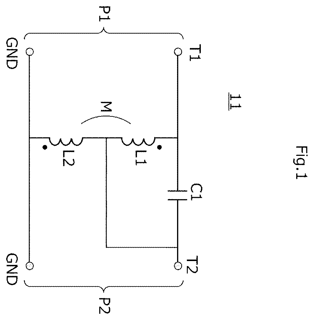
is a circuit diagram of a high pass filter 11 according to a first preferred embodiment of the present invention.
A to 2 D are circuit diagrams obtained by changing, in a sequential manner, the illustration form of the high pass filter 11 illustrated in .
A is a circuit diagram of a high pass filter 12 according to a second preferred embodiment of the present invention.
B is an equivalent circuit diagram in which a mutual inductance caused by magnetic coupling between a first inductor L 1 and a second inductor L 2 is expressed as a circuit element.
is a circuit diagram of a high pass filter 13 according to a third preferred embodiment of the present invention.
A and 5 B are equivalent circuit diagrams of the high pass filter 13 .
A and 6 B are diagrams illustrating frequency characteristics of a transmission coefficient of the high pass filter 13 .
is a perspective view of the high pass filter 13 .
includes exploded bottom views of individual insulator layers of the high pass filter 13 and conductive patterns formed on the insulator layers.
is a circuit diagram of a band rejection filter 14 A according to a fourth preferred embodiment of the present invention.
is a diagram illustrating frequency characteristics of the transmission coefficient of the high pass filter 11 illustrated in A to 2 D and frequency characteristics of the transmission coefficient of the band rejection filter 14 A illustrated in .
is an equivalent circuit diagram of a high pass filter 14 B, which is obtained by adding a capacitor C 3 to the high pass filter 13 .
is a diagram illustrating frequency characteristics of the transmission coefficient of the high pass filter 13 illustrated in and frequency characteristics of the transmission coefficient of the high pass filter, which is obtained by adding the capacitor C 3 to the high pass filter 13 .
is a circuit diagram of a band pass filter 14 C according to the fourth preferred embodiment of the present invention.
A to 14 D are block diagrams illustrating the configurations of filter modules.
is a block diagram illustrating the configuration of a high pass filter.
is a block diagram illustrating the configuration of a high pass filter.
is a block diagram illustrating the configuration of a high pass filter.
is a block diagram illustrating the configuration of a high pass filter.
is a block diagram illustrating the configuration of a high pass filter.
is a diagram illustrating frequency characteristics of the transmission coefficient of the high pass filter illustrated in , frequency characteristics of the transmission coefficient of only a high pass filter HPF in the high pass filter illustrated in , and frequency characteristics of the transmission coefficient of an anti-resonator (an LC series resonant circuit) in the high pass filter illustrated in .
is a perspective view of the high pass filter HPF in the high pass filter illustrated in .
includes exploded views of the high pass filter HPF illustrated in .
is a perspective view of the anti-resonator (the LC parallel resonant circuit) illustrated in .
includes exploded views of the anti-resonator (the LC parallel resonant circuit) illustrated in .
is an example of a cross-sectional view of a high pass filter 300 illustrated in .
is an example of a cross-sectional view of the high pass filter 300 illustrated in .
is an example of a cross-sectional view of the high pass filter 300 illustrated in .
is an example of a cross-sectional view of the high pass filter 300 illustrated in .
is an example of a cross-sectional view of the high pass filter 300 illustrated in .
is an equivalent circuit diagram of a high pass filter 400 .
is an equivalent circuit diagram of a high pass filter 500 .
is a perspective view of the high pass filter 500 .
includes exploded views of the high pass filter 500 .
is a block diagram illustrating the configuration of an electronic device 201 according to a sixth preferred embodiment of the present invention.
DETAILED DESCRIPTION OF THE PREFERRED EMBODIMENTS
Hereinafter, a plurality of preferred embodiments of the present invention will be illustrated by describing some specific examples with reference to the drawings. The same portions in the drawings are denoted by the same reference symbols. For the sake of convenience, the preferred embodiments are separately described by taking ease of description or understanding of main points into consideration. However, the configurations of different preferred embodiments among the preferred embodiments can be partially replaced with each other or combined. In second and subsequent preferred embodiments, the description of things common to a first preferred embodiment is omitted and only the points that differ from those of the first preferred embodiment will be described. In particular, substantially the same operational effects due to substantially the same configurations are not mentioned in every preferred embodiment.
First Preferred Embodiment
is a circuit diagram of a high pass filter 11 according to the first preferred embodiment. The high pass filter 11 is an example of a “filter” according to a preferred embodiment of the present invention.
The high pass filter 11 is a two-port network (a four-terminal network) including a first terminal pair P 1 and a second terminal pair P 2 . The first terminal pair P 1 includes a first terminal T 1 and a ground terminal GND. The second terminal pair P 2 includes a second terminal T 2 and a ground terminal GND.
The high pass filter 11 includes a first capacitor C 1 , a first inductor L 1 , and a second inductor L 2 . The first capacitor C 1 is connected in series between the first terminal pair P 1 and the second terminal pair P 2 . The first inductor L 1 is connected in parallel with the first capacitor C 1 . The second inductor L 2 is connected in parallel between the first terminal pair P 1 and the second terminal pair P 2 . The first inductor L 1 and the second inductor L 2 are magnetically coupled to each other and are differentially connected to each other.
A to 2 D are circuit diagrams obtained by changing, in a sequential manner, the illustration form of the high pass filter 11 illustrated in . A is a circuit diagram obtained by changing the illustration form of the high pass filter 11 illustrated in .
B is an equivalent circuit diagram in which a mutual inductance M caused by the magnetic coupling between the first inductor L 1 and the second inductor L 2 is expressed as a circuit element. As illustrated in B , when a circuit connected between the first terminal 11 and the second terminal T 2 is expressed as a T equivalent circuit including inductors LA, LB, and LC, the inductor LB, which expresses the mutual inductance M, is connected between the second terminal T 2 and a connection point where the series connected inductors LA and LC are connected to each other. Since the first inductor L 1 and the second inductor L 2 are differentially connected to each other, the inductance of the inductor LA is (L 1 −M), the inductance of the inductor LB is M, and the inductance of the inductor LC is (L 2 −M). A coupling coefficient between the first inductor L 1 and the second inductor L 2 is, for example, greater than or equal to about 0.2. In this case, when the inductance of the first inductor L 1 is denoted by L 1 , the inductance of the second inductor L 2 is denoted by L 2 , and the coupling coefficient is denoted by k, M=k√(L 1 ·L 2 ), and thus M≥about 0.2√(L 1 ·L 2 ). The coupling coefficient between the first inductor L 1 and the second inductor L 2 is, for example, less than or equal to about 0.8.
C is a circuit diagram obtained by converting, into a π circuit, the T circuit illustrated in B and including the inductors LA, LB, and LC. That is, the T circuit including the inductors LA, LB, and LC is expressed as a n circuit including inductors L 12 , L 1 M, and L 2 M. When the reference symbols of the inductors denote the inductances of the inductors, the relationships between the inductances of the individual inductors before and after the circuit is converted are as follows. L 1 M =( LA·LB+LB·LC+LC·LA )/ LC L 2 M =( LA·LB+LB·LC+LC·LA )/ LA L 12=( LA·LB+LB·LC+LC·LA )/ LB
D is a circuit diagram obtained by changing the illustration form of C . In this manner, the high pass filter 11 illustrated in can be expressed as a 3-stage n high pass filter illustrated in D .
According to the present preferred embodiment, the following operational effects are obtained.
As illustrated in A , since the first inductor L 1 and the first capacitor C 1 are connected in parallel, the parasitic capacitance generated in the first inductor L 1 is connected in parallel with (is acquired by) the first capacitor C 1 . Thus, the parasitic capacitance generated in the first inductor L 1 is effectively used, and bandpass characteristics in a high frequency band do not degrade due to self-resonance of the first inductor L 1 .
Since the parasitic capacitance of the first inductor L 1 can become part of the first capacitor C 1 , space can be saved accordingly. This enables downsizing. Alternatively, the extra space resulting from downsizing enables the line width of a coiled conductor of the first inductor L 1 and that of the second inductor L 2 to be increased or the coiled conductor of the first inductor L 1 and that of the second inductor L 2 to be wound in a parallel manner, thus increasing the Q factors of the inductors. This further increases the Q factor of the filter, so that insertion loss in the pass band can be further reduced, or attenuation in the stop band can be made deeper.
Since the mutual inductance generated due to the magnetic coupling between the first inductor L 1 and the second inductor L 2 serves as one circuit element, a high pass filter according to the present preferred embodiment is equivalent to a 3-stage π high pass filter in which an attenuation pole is generated at the second stage. In a general 3-stage n high pass filter, two inductors are present that are connected in parallel between the first terminal pair and the second terminal pair. Thus, parasitic capacitances are generated at these two locations (in parallel with L 12 and L 2 M in D in a respective manner), and the bandpass characteristics in the high frequency band may be degraded. In contrast, in the present preferred embodiment, one of the inductors is formed using the mutual inductance, and thus there is only one inductor (the second inductor L 2 ) for which parasitic capacitance becomes a problem. That is, in the equivalent circuit illustrated in D , a parasitic capacitance is not generated in parallel with the inductor L 12 but is generated in parallel with the inductor L 2 M. Thus, degradation of the bandpass characteristics can be reduced or prevented in the high frequency band.
Moreover, since the coupling coefficient is greater than or equal to about 0.2, a lossless mutual inductance increases in the filter circuit. Thus, even in a case where an equivalent series resistance (ESR) of a connection line and so forth is taken into consideration, an inductor having a significantly high Q factor can be provided, so that insertion loss in the pass band can be further reduced, or attenuation in the stop band can be made deeper. Moreover, the inductors do not need to be excessively spaced apart from each other. Thus, downsizing can be achieved by saving space, or the Q factors of the inductors can be increased, for example, by increasing the line widths of the coiled conductors or parallel winding the coiled conductors.
When the coupling coefficient is less than or equal to about 0.8, for example, a reduction in the total equivalent inductance (L 1 +L 2 −k√(L 1 ×L 2 )) through differential connection can be reduced. Thus, it becomes easier to ensure an inductance having a necessary magnitude, and an excessive space is unnecessary. As a result, downsizing is achieved or the Q factors of the inductors are increased. Furthermore, it is desirable that the coupling coefficient be less than about 0.5, for example. When the coupling coefficient is less than about 0.5, for example, it becomes easier to cause the inductances of the inductors LA, LB, and LC to have larger differences from each other in the equivalent circuit ( B ). The total inductance (L 1 M+L 2 M+L 12 ) of the post-conversion equivalent circuit ( D ) can be further increased. Thus, it becomes easier to ensure an inductance having a necessary magnitude, and an excessive space is unnecessary. As a result, downsizing is achieved or the Q factors of the inductors are increased. Moreover, it becomes possible to keep a sufficient distance between the first inductor L 1 and the second inductor L 2 , so that degradation of the bandpass characteristics in the high frequency band due to the parasitic capacitance between the inductors can be suppressed, and degradation of the Q factors of the inductors due to eddy-current loss can be reduced or prevented.
As illustrated in B , the inductors connected in a T shape are used as a basic configuration. Thus, compared with a case where the inductors connected in a n shape are used, for example, the inductance is reduced or the number of inductor elements is reduced by using a mutual inductance. Thus, use of the inductors connected in the T shape leads to downsizing or improved filter characteristics due to the increased Q factors of the inductors. (Insertion loss in the pass band is reduced, and attenuation in the stop band becomes deeper.)
By using a mutual inductance to form a portion of the equivalent circuit where a high Q factor is necessary, insertion loss in the pass band can be reduced, and attenuation in the stop band can be made deeper.
In the following, methods for determining the first inductor L 1 , the second inductor L 2 , and the coupling coefficient k will be described.
Method 1: Structural Determination Method
The shapes of electrodes of the internal inductors are confirmed through, for example, X-ray imaging or cross-sectioning, and each of the first inductor L 1 , the second inductor L 2 , and the mutual inductance M is calculated from the shapes of the electrodes of the inductors using Neumann's formula or other methods. Moreover, the coupling coefficient k is also calculated.
Alternatively, the shapes of the electrodes of the inductors are reproduced through a structure simulation, L 1 , L 2 , and M are obtained through numerical calculation from the distribution of current (or a vector potential, a magnetic field, magnetic flux) or network parameters (for example, an S parameter or a Z parameter) at the terminal pairs, and k is also calculated.
Method 2: Determination Method from Electrical Characteristics Measurable at Terminals
L 1 , L 2 , and M are obtained, using a network analyzer, from the network parameters at the terminal pairs, and k is also calculated.
Alternatively, L 1 , L 2 , and M are obtained, using for example an impedance analyzer or an LCR meter, from input impedances between the terminals, and k is also calculated. In this case, it is desirable that measurements be performed at low frequencies (on the order of 100 MHz to 1 GHz) in order to avoid the effect of parasitic capacitance on the measurement system. (Note that when the frequency is too low, measurements cannot be performed because the impedances become too low.)
Second Preferred Embodiment
In a second preferred embodiment, an example of a high pass filter including a third inductor will be illustrated.
A is a circuit diagram of a high pass filter 12 according to the second preferred embodiment. B is an equivalent circuit diagram in which a mutual inductance M caused by the magnetic coupling between the first inductor L 1 and the second inductor L 2 is expressed as a circuit element.
The high pass filter 12 includes the first capacitor C 1 , the first inductor L 1 , and a third inductor L 3 . The first capacitor C 1 is connected in series between the first terminal pair P 1 and the second terminal pair P 2 . The first inductor L 1 is connected in parallel with the first capacitor C 1 . An end of the second inductor L 2 is connected between the first terminal pair P 1 and the second terminal pair P 2 . The third inductor L 3 and the first inductor L 1 define a series circuit, and this series circuit is connected in series between the first terminal pair P 1 and the second terminal pair P 2 . The first inductor L 1 and the second inductor L 2 are magnetically coupled to each other and are differentially connected to each other.
As illustrated in B , when a circuit including the first inductor L 1 and the second inductor L 2 is expressed as a T equivalent circuit including the inductors LA, LB, and LC, the inductor LB, which expresses the mutual inductance M, is connected between the second terminal T 2 and a connection point where the series connected inductors LA and LC are connected to each other. Since the first inductor L 1 and the second inductor L 2 are differentially connected to each other, the inductance of the inductor LA is (L 1 −M), the inductance of the inductor LB is M, and the inductance of the inductor LC is (L 2 −M).
In this manner, the third inductor L 3 is equivalently connected in series with the inductor LB. As a result, the level of balance between the Q factors of the inductors LA, LB+L 3 , and LC can be freely determined, and a filter having desired filter characteristics can be configured. On the basis of this configuration, characteristics of the high pass filter may be determined.
Third Preferred Embodiment
In a third preferred embodiment, an example of a 4-stage high pass filter will be illustrated.
is a circuit diagram of a high pass filter 13 according to the third preferred embodiment. The high pass filter 13 includes the first capacitor C 1 , the first inductor L 1 , the second inductor L 2 , and a second capacitor C 2 . The first capacitor C 1 is connected in series between the first terminal pair P 1 and the second terminal pair P 2 . The first inductor L 1 is connected in parallel with the first capacitor C 1 . The second inductor L 2 is connected in parallel between the first terminal pair P 1 and the second terminal pair P 2 . The second capacitor C 2 is connected between the second terminal pair P 2 and the first capacitor C 1 . The first inductor L 1 and the second inductor L 2 are magnetically coupled to each other and are differentially connected to each other. A and 5 B are equivalent circuit diagrams of the high pass filter 13 . The high pass filter 13 differs from the high pass filter 11 illustrated in in the first preferred embodiment in that the high pass filter 13 includes the second capacitor C 2 .
A is an equivalent circuit diagram in which a mutual inductance caused by the magnetic coupling between the first inductor L 1 and the second inductor L 2 is expressed as a circuit element. In the equivalent circuit illustrated in A , differences regarding a transmission coefficient of the high pass filter 13 due to differences between the Q factors of the individual inductors will be as follows.
A and 6 B are diagrams illustrating frequency characteristics of the transmission coefficient of the high pass filter 13 according to the present preferred embodiment. The horizontal axes of A and 6 B represent frequency, and the vertical axes of A and 6 B represent values of a transmission coefficient S 21 . B is an enlarged view of a portion enclosed in the oblong figure in A .
As illustrated in A , the high pass filter 13 has the 6.24 GHz band and the 8.2 GHz band, which are used in UWB, as its pass bands and serves as a high pass filter having an insertion loss of about −3 dB at a cutoff frequency of about 5.6 GHz. In B , characteristics A are characteristics in a case where the Q factor of the inductor LA illustrated in A is low. Characteristics B are characteristics in a case where the Q factor of the inductor LB illustrated in A is low. Characteristics C are characteristics in a case where the Q factor of the inductor LC illustrated in A is low. Moreover, characteristics N are characteristics in a case where the inductors LA, LB, and LC illustrated in A are lossless.
As is clear from comparison between the characteristics A and B, the Q factor of the inductor LB affects insertion loss more greatly than the Q factor of the inductor LA. Moreover, the Q factor of the inductor LB affects the steepness from the attenuation band to the pass band more greatly than the Q factor of the inductor LA. Thus, as illustrated in A , insertion loss can be reduced over a wide band of the pass band by forming the inductor LB with the mutual inductance (M), which is lossless.
B is a circuit diagram obtained by converting, into a n circuit, the T circuit illustrated in A and including the inductors LA, LB, and LC. That is, the T circuit including the inductors LA, LB, and LC is expressed as a n circuit including the inductors L 12 , L 1 M, and L 2 M. With this configuration, a 4-stage high pass filter is configured.
Values of individual elements included in the high pass filter 13 illustrated in and the coupling coefficient k between the first inductor L 1 and the second inductor L 2 are as follows.
•
• L 1 : 1.2 nH • L 2 : 0.9 nH • C 1 : 0.75 pF • C 2 : 0.56 pF • k: 0.32
In this case, values of the individual elements included in the equivalent circuit illustrated in B are as follows.
•
• L 12 : 2.8 nH • L 1 M: 1.6 nH • L 2 M: 1.1 nH • C 1 : 0.75 pF • C 2 : 0.56 pF
In this case, the total inductance of the inductors L 12 , L 1 M, and L 2 M is about 5.6 nH, whereas the total inductance of the first inductor L 1 and the second inductor L 2 is about 2.1 nH, for example. Thus, the total inductance can be reduced by as much as about 63%, for example. In the equivalent circuit illustrated in B , the total inductance of paths which are shunt-electrically connected to ground is about 3.9 nH, for example, and thus even only by making a comparison with this shunt connection portion, the inductance can be reduced by about half. This enables overall downsizing and increases the amount of attenuation in the attenuation band. “Ground” in this specification is a reference potential portion in a circuit and refers to electrical ground.
is a perspective view of the high pass filter 13 . The high pass filter 13 has a rectangular or substantially rectangular parallelepiped-shaped multilayer body 1 in which a plurality of rectangular or substantially rectangular insulator layers are stacked. On the outer surface of the multilayer body 1 , for example, a first terminal electrode ET 1 , a second terminal electrode ET 2 , a ground terminal electrode (a terminal hidden behind an object in ), and a floating terminal electrode ENC are formed by plating. The floating terminal electrode ENC is used for interlayer connection between internal electrodes.
The first inductor L 1 includes a first coiled conductor CL 1 in the multilayer body 1 including a plurality of insulator layers. The second inductor L 2 includes a second coiled conductor CL 2 in the multilayer body 1 including a plurality of insulator layers. The first coiled conductor CL 1 of the first inductor L 1 includes a first coil cavity CP 1 . The second coiled conductor CL 2 of the second inductor L 2 includes a second coil cavity CP 2 .
The winding axis of the first coiled conductor CL 1 is parallel or substantially parallel to that of the second coiled conductor CL 2 . The coil cavity CP 1 of the first coiled conductor CL 1 and the coil cavity CP 2 of the second coiled conductor CL 2 have an overlapping region when viewed in the winding axis direction. With this structure, the first inductor L 1 and the second inductor L 2 are magnetically coupled to each other.
The first capacitor C 1 includes first capacitor electrodes EC 1 and insulator layers. The first capacitor electrodes EC 1 face each other in the stacking direction of the plurality of insulator layers. The insulator layers are sandwiched between these first capacitor electrodes. The second capacitor C 2 includes second capacitor electrodes EC 2 and insulator layers. The second capacitor electrodes EC 2 face each other in the stacking direction of the plurality of insulator layers. The insulator layers are sandwiched between these second capacitor electrodes.
includes exploded bottom views of individual insulator layers of the high pass filter 13 and conductive patterns located on the insulator layers.
The multilayer body 1 is defined by laminating insulator layers S 1 to S 12 . illustrates views of the individual insulator layers as viewed from the mounting terminal side. The insulator layer S 1 is the uppermost insulator layer, and the insulator layer S 12 is the lowermost insulator layer. The insulator layers S 2 to S 11 are insulator layers between the uppermost insulator layer S 1 and the lowermost insulator layer S 12 .
Side terminal electrodes E 1 , E 2 , E 3 , and E 4 are formed on the insulator layers S 1 to S 12 . The side terminal electrodes E 1 , E 2 , E 3 , and E 4 formed on the individual base layers are electrically connected to the terminal electrodes denoted by the same symbols. The side terminal electrodes E 1 , the side terminal electrodes E 2 , and the side terminal electrodes E 3 are electrically connected to the first terminal electrode ET 1 , the second terminal electrode ET 2 , and the floating terminal electrode ENC illustrated in , respectively. The side terminal electrodes E 4 are electrically connected to the ground terminal electrode.
Second coiled conductors CL 2 a , CL 2 b , CL 2 c , and CL 2 d formed on the insulator layers S 1 to S 4 define the second coiled conductor CL 2 illustrated in . Similarly, first coiled conductors CL 1 a , CL 1 b , CL 1 c , and CL 1 d formed on the insulator layers S 8 to S 11 define the first coiled conductor CL 1 .
First capacitor electrodes EC 1 a , EC 1 b , and EC 1 c formed on the insulator layers S 1 to S 3 and first capacitor electrodes EC 1 d and EC 1 e formed on the insulator layers S 9 and S 10 define the first capacitor C 1 . Second capacitor electrodes EC 2 a , EC 2 b , and EC 2 c formed on the insulator layers S 5 , S 6 , and S 7 define the second capacitor C 2 .
An end of the second coiled conductor CL 2 a and an end of the second coiled conductor CL 2 b are each electrically connected to the side terminal electrode E 4 . An end of the second coiled conductor CL 2 c is electrically connected to the side terminal electrode E 3 with the first capacitor electrode EC 1 c interposed therebetween, and an end of the second coiled conductor CL 2 d is electrically connected to the side terminal electrode E 3 .
An end of the first coiled conductor CL 1 a is electrically connected to the side terminal electrode E 3 , and an end of the first coiled conductor CL 1 b is electrically connected to the side terminal electrode E 3 with the capacitor electrode EC 1 d interposed therebetween. An end of the first coiled conductor CL 1 c is electrically connected to the side terminal electrode E 1 with the capacitor electrode EC 1 e interposed therebetween, and an end of the first coiled conductor CL 1 d is electrically connected to the side terminal electrode E 1 .
In this manner, the first coiled conductors CL 1 b and CL 1 c and the first capacitor electrodes EC 1 d and EC 1 e are defined by continuous conductive patterns. With this structure, a parasitic capacitance generated between the first coiled conductor CL 1 b and the first coiled conductor CL 1 c can be used as part of the first capacitor C 1 . Thus, the first capacitor electrodes EC 1 d and EC 1 e can be reduced in size, and the overall size can be reduced accordingly. Alternatively, the extra space resulting from downsizing enables the line width of the coiled conductors of the first inductor to be increased, thus increasing the Q factor of the first inductor and improving the filter characteristics. (Insertion loss in the pass band can be reduced, and attenuation in the stop band can be made deeper.)
In this manner, the first coiled conductors CL 1 b and CL 1 c and the first capacitor electrodes EC 1 d and EC 1 e are defined by continuous conductive patterns. With this structure, a parasitic capacitance generated between the first coiled conductor CL 1 b and the first coiled conductor CL 1 c can be used as part of the first capacitor C 1 . Thus, the first capacitor electrodes EC 1 d and EC 1 e can be reduced in size, and the overall size can be reduced accordingly. Alternatively, the extra space resulting from downsizing enables the line width of the coiled conductors of the first inductor to be increased, thus further increasing the Q factor of the filter and further reducing insertion loss.
A wiring conductor WC is provided between the second capacitor electrode EC 2 b and the side terminal electrode E 2 . The wiring conductor WC is a conductor connected in series between the second capacitor C 2 and the second terminal 12 . In this manner, the wiring conductor WC is spaced apart from the coiled conductors CL 1 and CL 2 in the stacking direction. This structure helps to suppress parasitic capacitance generated between the wiring conductor WC and the coiled conductors CL 1 and CL 2 (especially the second coiled conductor CL 2 ). Moreover, this helps to prevent the wiring conductor WC from blocking magnetic flux generated from the coiled conductors CL 1 and CL 2 , so that a reduction in the Q factor of the first inductor L 1 and/or a reduction in that of the second inductor L 2 is suppressed or prevented.
Moreover, the wiring conductor WC has a conductor width smaller than at least one of the conductor width of the first coiled conductors CL 1 a , CL 1 b , CL 1 c , and CL 1 d or the conductor width of the second coiled conductors CL 2 a , CL 2 b , CL 2 c , and CL 2 d . With this structure, a parasitic capacitance generated between the wiring conductor WC and another conductor adjacent to the wiring conductor WC in the stacking direction is further reduced or prevented. This structure helps to prevent the wiring conductor WC from blocking magnetic flux generated by the coiled conductors CL 1 and CL 2 , so that a reduction in the Q factor of the first inductor L 1 and/or a reduction in that of the second inductor L 2 is suppressed or prevented.
As illustrated in or , an (E 1 side) end portion of the first coiled conductor CL 1 and an (E 4 side) end portion of the second coiled conductor CL 2 are spaced apart from each other with the first coiled conductor CL 1 , the second coiled conductor CL 2 , and the connection portions of the first and second coiled conductors CL 1 and CL 2 interposed therebetween. Thus, the ends of the coils are not close to each other, and the coils themselves serve as shields, so that the parasitic capacitance between the coils and the effects of the parasitic capacitance are reduced or prevented. Thus, degradation of the bandpass characteristics is reduced or prevented in the high frequency band.
Fourth Preferred Embodiment
In a fourth preferred embodiment, an example of a filter module will be illustrated.
is a circuit diagram of a band rejection filter 14 A according to the fourth preferred embodiment. The band rejection filter 14 A has a configuration in which the high pass filter 11 illustrated in A is provided with a capacitor C 3 . The capacitor C 3 is connected in series with the second inductor L 2 , which is provided along a path which is shunt-electrically connected to ground. As a result, a configuration is obtained in which the series resonant circuit which is shunt-electrically connected to ground. This series resonant circuit causes a current to flow to ground at a specific frequency, and thus this whole configuration serves as a band rejection filter.
is a diagram illustrating frequency characteristics of the transmission coefficient of the high pass filter 11 illustrated in and frequency characteristics of the transmission coefficient of the band rejection filter 14 A illustrated in . As illustrated in , two attenuation poles appear in the band rejection filter 14 A illustrated in , and thus it is clear that the band rejection filter 14 A functions as a band rejection filter.
is an equivalent circuit diagram of a high pass filter 14 B, which is obtained by adding the capacitor C 3 to the high pass filter 13 . is a diagram illustrating frequency characteristics of the transmission coefficient of the high pass filter 13 illustrated in and frequency characteristics of the transmission coefficient of the high pass filter 14 B, which is obtained by adding the capacitor C 3 to the high pass filter 13 . As a result, the high pass filter 14 B, which is obtained by adding the capacitor C 3 to the high pass filter 13 , serves as a high pass filter having two attenuation poles.
is a circuit diagram of a band pass filter 14 C according to the fourth preferred embodiment. The band pass filter 14 C has a configuration in which the high pass filter illustrated in A is provided with an inductor L 4 . The inductor L 4 is connected in series with the capacitor C 1 provided along a path connected s with a signal line. As a result, a configuration is obtained in which the series resonant circuit is connected in series with the signal line. This series resonant circuit allows passage at specific frequencies, and thus this whole configuration serves as a band pass filter.
Note that, in , 11 , and 13 , filter modules are configured by adding a capacitor or an inductor to the circuit illustrated in A as a base. However, these are examples. Other than these filter modules, for example, a band pass filter may be configured by providing the inductor L 4 along the path connected in series with the signal line in .
Fifth Preferred Embodiment
In a fifth preferred embodiment, another example of a filter module will be described.
A is a block diagram illustrating the configuration of a band pass filter. This band pass filter has a configuration in which a high pass filter HPF and a low pass filter LPF are cascade connected. This high pass filter HPF includes any one of the high pass filters described in the first and second preferred embodiments.
B a block diagram illustrating the configuration of a band rejection filter. This band rejection filter has a configuration in which a high pass filter HPF and a low pass filter LPF are connected in parallel. This high pass filter HPF includes any one of the high pass filters described in the first and second preferred embodiments.
C is a block diagram illustrating the configuration of a diplexer. This diplexer includes a high pass filter HPF and a low pass filter LPF. An end of the high pass filter HPF and an end of the low pass filter LPF are connected so as to provide a common connection. This high pass filter HPF includes any one of the high pass filters described in the first and second preferred embodiments.
D is a block diagram illustrating the configuration of a triplexer. This triplexer includes a high pass filter HPF, a band pass filter BPF, and a low pass filter LPF. An end of the high pass filter HPF, an end of the band pass filter BPF, and an end of the low pass filter LPF are connected so as to provide a common connection. This high pass filter HPF includes any one of the high pass filters described in the first and second preferred embodiments.
Note that a multiplexer can be configured in the same manner as in the examples illustrated in C and 14 D .
is a block diagram illustrating the configuration of a high pass filter. In this high pass filter, two high pass filters HPF are cascade connected. The two high pass filters HPF are each including any one of the high pass filters illustrated in the first and second preferred embodiments. Moreover, one of the two high pass filters HPF may be a high pass filter other than the high pass filters described in the first and second preferred embodiments.
block is a diagram illustrating the configuration of a high pass filter. This high pass filter includes a high pass filter HPF and a capacitor C. The capacitor C is connected in series with an end of one of the terminal pairs of the high pass filter HPF. That is, in this high pass filter, the high pass filter HPF and the capacitor C, which is connected in series with the high pass filter HPF, are cascade connected. The high pass filter HPF includes any one of the high pass filters described in the first and second preferred embodiments.
is a block diagram illustrating the configuration of a high pass filter. This high pass filter includes a high pass filter HPF and an inductor L. An end of the inductor L is connected to an end of one of the terminal pairs of the high pass filter HPF. The other end of the inductor L is connected to ground, that is, to the other end of the one of the terminal pairs of the high pass filter HPF. That is, in this high pass filter, the high pass filter HPF and the inductor L, which is connected in parallel with the high pass filter HPF, are cascade connected. The high pass filter HPF includes any one of the high pass filters described in the first and second preferred embodiments.
is a block diagram illustrating the configuration of a high pass filter. This high pass filter includes a high pass filter HPF and an anti-resonator (an LC parallel resonant circuit). The anti-resonator (the LC parallel resonant circuit) includes a parallel connection circuit including an inductor L and a capacitor C. The anti-resonator (the LC parallel resonant circuit) is connected in series with an end of one of the terminal pairs of the high pass filter HPF. That is, in this high pass filter, the high pass filter HPF and the anti-resonator (the LC parallel resonant circuit), which is connected in series with the high pass filter HPF, are cascade connected. The high pass filter HPF includes any one of the high pass filters described in the first and second preferred embodiments.
is a block diagram illustrating the configuration of a high pass filter. This high pass filter includes a high pass filter HPF and a resonator (an LC series resonant circuit). The resonator (the LC series resonant circuit) includes a series connection circuit including an inductor L and a capacitor C. An end of the resonator (the LC series resonant circuit) is connected to an end of one of the terminal pairs of the high pass filter HPF. The other end of the resonator (the LC series resonant circuit) is connected to ground, that is, to the other end of the one of the terminal pairs of the high pass filter HPF. That is, in this high pass filter, the high pass filter HPF and the resonator (the LC series resonant circuit), which is connected in parallel with the high pass filter HPF, are cascade connected. The high pass filter HPF includes any one of the high pass filters described in the first and second preferred embodiments.
In this case, is a diagram illustrating frequency characteristics of the transmission coefficient of the high pass filter illustrated in , frequency characteristics of the transmission coefficient of only the high pass filter HPF in the high pass filter illustrated in , and frequency characteristics of the transmission coefficient of only the anti-resonator (the LC parallel resonant circuit) connected in series in the high pass filter illustrated in .
As illustrated in , only one attenuation pole is located in the frequency characteristics of the transmission coefficient of only the high pass filter HPF in the high pass filter illustrated in , and in the frequency characteristics of the transmission coefficient of only the anti-resonator (the LC parallel resonant circuit) connected in series in the high pass filter illustrated in . In contrast, two attenuation poles are formed in the frequency characteristics of the transmission coefficient of the high pass filter illustrated in .
is a perspective view of the high pass filter HPF in the high pass filter illustrated in . includes exploded views of the high pass filter HPF illustrated in . is a perspective view of the anti-resonator (the LC parallel resonant circuit) illustrated in . includes exploded views of the anti-resonator (the LC parallel resonant circuit) illustrated in .
As illustrated in , the first inductor L 1 is located in the lower portion of the multilayer body of the high pass filter HPF. The inductor L 1 is located in the left portions and the central portions of the insulator layers S 7 to S 11 . The inductor L 1 has a structure in which the conductor layers provided on the insulator layers S 7 to S 11 are connected by interlayer connection conductors v 14 to v 17 . The first inductor L 1 is connected to the first terminal electrode ET 1 and the first capacitor C 1 .
The second inductor L 2 is positioned above the first inductor L 1 . The inductor L 2 is provided in the left portions of the insulator layers S 1 to S 4 . The inductor L 2 has a structure in which the conductor layers provided on the insulator layers S 1 to S 4 are connected by interlayer connection conductors v 11 to v 13 . The second inductor L 2 is connected to a ground terminal EG and the first terminal electrode ET 1 .
The first capacitor C 1 is positioned to the right of the first inductor L 1 and the second inductor L 2 . In the first capacitor C 1 , a plurality of rectangular conductor layers on the respective insulator layers S 1 to S 11 are superposed with each other in the up-down direction. The first capacitor C 1 is connected to the second terminal electrode ET 2 and the floating terminal electrode ENC. Note that the four corners of the insulator layers S 1 to S 12 are provided with interlayer connection conductors.
As illustrated in , the capacitor C 2 is divided into a left side and a right side. In the capacitor C 2 , a plurality of rectangular or substantially rectangular conductor layers on the respective left and right portions of the insulator layers S 1 to S 11 are superposed with each other in the up-down direction. The second capacitor C 2 is connected to the terminal electrode T 1 and the inductor L 3 .
The inductor L 3 is provided within the capacitor C 2 . More specifically, the inductor L 3 is formed or located in the central portions of the insulator layers S 1 to S 10 . The inductor L 3 has a structure in which the conductor layers provided on the insulator layers S 1 to S 10 are connected by interlayer connection conductors v 21 to v 25 . The third inductor L 3 is connected to the terminal electrode 12 and the second capacitor C 2 . Note that the four corners of the insulator layers S 1 to S 12 are provided with interlayer connection conductors.
A capacitor electrode that overlaps the cavity of a coil serving as the inductor L is not disposed in the high pass filter HPF or the anti-resonator (the LC parallel resonant circuit). This enables loss due to an eddy current caused by a capacitor electrode to be reduced or prevented in the inductor L, and the Q factor of the inductor L to be increased. In the high pass filter HPF, capacitor electrodes are arranged outside the coil and on the same layers as the coil electrodes when viewed from the winding axis direction of the coil. In the anti-resonator (the LC parallel resonant circuit), the outermost winding portion of the coil electrode of each layer is thicker than the other portion such that the outermost winding portion of the coil electrode of each layer also serves as a capacitor electrode. As a result, the coil electrode and the capacitor electrode are integrated with each other. Thus, the spacing between the coil electrode and the capacitor electrode becomes unnecessary, and the size of the coil shape can be increased, thus enabling the Q factor of the inductor L to be increased. With these configurations, it is thus easy to increase the Q factors of the inductors of the high pass filter HPF and the anti-resonator (the LC parallel resonant circuit). As a result, high frequency signal loss in the pass band becomes low, and high frequency signal loss outside the pass band becomes high. Furthermore, the attenuation poles become deeper.
is an example of a cross-sectional view of a high pass filter 300 , which is illustrated in . The high pass filter 300 includes a substrate 310 and the high pass filter HPF. The high pass filter HPF is mounted on the substrate 310 . The anti-resonator (the LC parallel resonant circuit) is defined by conductor layers and interlayer connection conductors provided in the substrate 310 . Since the high pass filter HPF and the anti-resonator (the LC parallel resonant circuit) are not superposed with each other when viewed from the stacking direction of the substrate 310 , a reduction in the Q factor of the inductor of the high pass filter HPF and a reduction in the Q factor of the inductor of the anti-resonator (the LC parallel resonant circuit) are suppressed or prevented.
is an example of a cross-sectional view of the high pass filter 300 , which is illustrated in . The high pass filter 300 includes the substrate 310 , the high pass filter HPF, and the capacitor. The high pass filter HPF and the capacitor are mounted on the substrate 310 . The capacitor is, for example, a multilayer ceramic capacitor. The inductor is defined by the conductor layers and the interlayer connection conductors provided in the substrate 310 . The capacitor and the inductor define the anti-resonator (the LC parallel resonant circuit). By using a mounting component as part of the anti-resonator (the LC parallel resonant circuit), a capacitor with a high capacitance can be used. The degree of freedom in the design of the high pass filter 300 is thus increased. Moreover, the Q factor of the inductor is increased.
is an example of a cross-sectional view of the high pass filter 300 , which is illustrated in . The high pass filter 300 includes the substrate 310 , the high pass filter HPF, and the inductor. The high pass filter HPF and the inductor are mounted on the substrate 310 . The capacitor is defined by conductor layers provided in the substrate 310 . The capacitor and the inductor form the anti-resonator (the LC parallel resonant circuit). By using a mounting component as part of the anti-resonator (the LC parallel resonant circuit), an inductor with a high inductance can be used. The degree of freedom in the design of the high pass filter 300 is thus increased. Moreover, the Q factor of the inductor is increased.
is an example of a cross-sectional view of the high pass filter 300 , which is illustrated in . The high pass filter 300 includes the substrate 310 and the high pass filter HPF. The high pass filter HPF is mounted on the substrate 310 . The anti-resonator (the LC parallel resonant circuit) is defined by conductor layers and interlayer connection conductors provided in the substrate 310 . The anti-resonator (the LC parallel resonant circuit) is superposed with the high pass filter HPF when viewed from the stacking direction of the substrate 310 . The inductor of the anti-resonator (the LC parallel resonant circuit) is thus magnetically coupled to the inductor of the high pass filter HPF (the LC parallel resonant circuit). As a result, the degree of freedom in the design of the high pass filter 300 is increased. Moreover, it becomes possible to reduce the L value of the high pass filter 300 , and an inductor can be designed to have a structure (a parallel wound structure, a thickly wound structure, or the like) having a high Q factor.
is an example of a cross-sectional view of the high pass filter 300 illustrated in . The high pass filter 300 includes the substrate 310 , the high pass filter HPF, and the capacitor. The high pass filter HPF and the capacitor are mounted on the substrate 310 . The inductor is defined by conductor layers and interlayer connection conductors provided in the substrate 310 . The anti-resonator (the LC parallel resonant circuit) is defined by the inductor and the capacitor. The inductor is superposed with the high pass filter HPF when viewed from the stacking direction of the substrate 310 . The inductor of the anti-resonator (the LC parallel resonant circuit) is thus magnetically coupled to the inductor in the substrate 310 . As a result, the degree of freedom in the design of the high pass filter 300 is increased. Moreover, it becomes possible to reduce the L value of the high pass filter 300 , an inductor can be designed to have a structure (a parallel wound structure, a thickly wound structure, or the like) having a high Q factor.
is an equivalent circuit diagram of a high pass filter 400 . is an equivalent circuit diagram of a high pass filter 500 . The high pass filter 400 illustrated in is a 5-stage transformer HPF circuit. The high pass filter 400 has four external terminals. However, the high pass filter 400 has five nodes. Thus, the number of nodes is larger than the number of external terminals. Nodes p 1 , p 2 , and G are connected to external circuits. Thus, nodes N 1 and N 2 are defined by the remaining one external terminal and internal connection. Thus, either one of the nodes N 1 and N 2 has a structure in which interlayer connection is provided inside or is a structure without an interlayer connection.
In a case where interlayer connection is provided inside, interlayer connection conductors, a via reception conductor layer, and a space for the interlayer connection conductors and other conductor layers are necessary. Thus, degradation of the Q factor due to an increased equivalent series inductance (ESL), an increased ESR, and reduced space may significantly degrade the filter characteristics. In order to avoid such degradation of the characteristics, the high pass filter 400 that has a structure without interlayer connection was studied.
Furthermore, in a case where a high coupling coefficient (for example, k=about 0.4 to about 0.9) is necessary, when two inductors are simply arranged in the up-down direction, the gap between the layers of the two inductors needs to be reduced to increase the coupling coefficient. Since the two inductors are close to each other, the Q factors of the inductors become low. A structure will also be studied with which a reduction in Q factor is small while increasing the coupling coefficient.
The high pass filter 500 has the equivalent circuit illustrated in . This enables the number of interlayer connection conductors to be reduced. As a result, reductions in the Q factors of the inductors are suppressed or prevented.
In the following, the structure of the high pass filter 500 illustrated in will be described with reference to the drawings. is a perspective view of the high pass filter 500 . includes exploded views of the high pass filter 500 .
As illustrated in , the high pass filter 500 has a structure in which internal electrode layers, insulator layers, and interlayer connection conductors between the internal electrode layers are vertically symmetrical, the insulator layers being positioned between the internal electrode layers. Inductors L 1 a and Lga, capacitors C 1 a and C 2 a , and half of a capacitor C 0 are located in the upper half portion of the high pass filter 500 . Inductors L 1 b and Lgb, capacitors C 1 b and C 2 b , and half of the capacitor C 0 are located in the lower half portion of the high pass filter 500 . As illustrated in , the high pass filter 500 is a circuit obtained by dividing the two-port network from the node N 1 to the node p 2 of the circuit of the high pass filter 400 illustrated in into circuits that are connected in parallel with each other. The circuits obtained by division each have half the capacitance of the capacitor, two times the inductance of the inductor, and the same coupling coefficient. That is, C 1 a =C 1 b =C 1 /2, C 2 a =C 2 b =C 2 /2, L 1 a =L 1 b =L 1 ×2, and Lga=Lgb=Lg×2.
The capacitor C 0 is located on the left half portions of the insulator layers S 1 to S 4 and S 8 to S 11 . The inductor Lga is, located on the right half portions of the insulator layers S 1 and S 2 . The inductor Lga has a structure in which the conductor layer provided on the insulator layer S 1 and the conductor layer provided on the insulator layer S 2 are connected by an interlayer connection conductor v 1 .
The capacitor C 1 a is located on the left half portions of the insulator layers $4 and S 5 . The capacitor C 1 a is located between the conductor layer provided on the insulator layer S 4 and the conductor layer provided on the insulator layer S 5 . The capacitor C 2 a is located on the left half portions of the insulator layers S 5 and S 6 . The capacitor C 2 a is located between the conductor layer provided on the insulator layer S 5 and the conductor layer provided on the insulator layer S 6 .
The inductor L 1 a is located on the right half portions of the insulator layers S 4 and S 5 . The inductor L 1 a has a structure in which the conductor layer provided on the insulator layer S 4 and the conductor layer provided on the insulator layer S 5 are connected by an interlayer connection conductor v 2 .
The inductor Lgb is located on the right half portions of the insulator layers S 10 and S 11 . The inductor Lgb has a structure in which the conductor layer provided on the insulator layer S 10 and the conductor layer provided on the insulator layer S 11 are connected by an interlayer connection conductor v 3 .
The capacitor C 1 b is located on the left half portions of the insulator layers S 7 and S 8 . The capacitor C 1 b is located between the conductor layer provided on the insulator layer S 7 and the conductor layer provided on the insulator layer S 8 . The capacitor C 2 b is located on the left half portions of the insulator layers S 7 and S 6 . The capacitor C 2 b is located between the conductor layer provided on the insulator layer S 7 and the conductor layer provided on the insulator layer S 6 .
The inductor L 1 b is located in the right half portions of the insulator layers S 7 and S 8 . The inductor L 1 b has a structure in which the conductor layer provided on the insulator layer S 7 and the conductor layer provided on the insulator layer S 8 are connected by an interlayer connection conductor V 3 . Note that the four corners of the insulator layers S 1 to S 12 are provided with interlayer connection conductors. The high pass filter 500 as described above is manufactured by, for example, repeatedly performing a photolithographic process.
In the high pass filter 500 as described above, the conductor layer provided on the insulator layer S 5 serves as both the conductor layer serving as the capacitor C 1 a and the conductor layer serving as the capacitor C 2 a . Thus, an interlayer connection conductor for connecting the capacitor C 1 a to the capacitor C 2 a is unnecessary. As a result, the high pass filter 500 has a structure in which there is not an interlayer connection conductor other than the interlayer connection conductors provided in the inductors. Moreover, since the inductors L 1 a and L 1 b are positioned between the inductor Lga and the inductor Lgb, the layer gap between the coils can be increased while increasing the coupling coefficient between the inductor L 1 a and the inductor L 1 b , so that high Q of inductors can be realized.
Sixth Preferred Embodiment
In a sixth preferred embodiment, an example of an electronic device will be illustrated, the electronic device including a filter circuit device or a filter circuit module among the filter circuit devices or the filter circuit modules described above.
is a block diagram illustrating the configuration of an electronic device 201 according to the sixth preferred embodiment. The electronic device 201 is, for example, a so-called smartphone or a cellular phone. The electronic device 201 includes a duplexer 53 , an antenna 54 , a control circuit 50 , an interface and a memory 51 , and a frequency synthesizer 52 . The transmission system includes a transmitter 61 , a transmission signal processing circuit 62 , a transmission mixer 63 , a transmission filter 64 , and a power amplifier 65 . The reception system includes a low noise amplifier 71 , a reception filter 72 , a reception mixer 73 , a reception signal processing circuit 74 , and a receiver 75 . A transmission signal output from the power amplifier 65 is output to the antenna 54 via the duplexer 53 . Moreover, a signal received by the antenna 54 passes through the duplexer 53 and is then amplified by the low noise amplifier 71 . Note that in a case where a call is not made and data communication or the like is performed, the control circuit 50 processes a reception signal.
A filter or a filter module according to preferred embodiments of the present invention can be included in the transmission filter 64 or the reception filter 72 . Moreover, a filter or a filter module according to preferred embodiments of the present invention can be included in a high frequency side filter of the duplexer 53 .
Moreover, in a case where filters are provided, for example, before and after the power amplifier 65 , before and after the low noise amplifier 71 , before and after the transmission mixer 63 , and before and after the reception mixer 73 , filters or filter modules according to preferred embodiments the present invention can be included in these filters.
Current smartphones and cellular phones are used through a plurality of antennas or in a plurality of frequency bands, and thus many band pass filters or many wave separators are used. As these band pass filters or wave separators, for example, the band pass filter, the diplexer, the triplexer, or the multiplexer described in the fifth preferred embodiment can be used.
While preferred embodiments of the present invention have been described above, it is to be understood that variations and modifications will be apparent to those skilled in the art without departing from the scope and spirit of the present invention. The scope of the present invention, therefore, is to be determined solely by the following claims.
Figures (20)
Citations
This patent cites (15)
- US6998939
- US2006/0145782
- US2009/0009267
- US2013/0076454
- US2013/0328642
- US2021/0050837
- US602654
- US2006186621
- US2013070288
- US2020058044
- US2006085624
- US2012121038
- US2017199745
- US2018150881
- US2019235261