Multi-finger Transistor and Power Amplifier Circuit
Abstract
A multi-finger transistor includes unit transistors each including a first terminal electrically connected to a reference potential, a second terminal that receives an RF signal and a bias current, and a third terminal that outputs an amplified signal; a common input terminal electrically connected in parallel to the second terminals of the unit transistors and that receives the RF signal; a common bias terminal electrically connected in parallel to the second terminals of the unit transistors and that receives the bias current; a common output terminal electrically connected in parallel to the third terminals of the unit transistors and that outputs the amplified signal; and first resistance elements each of which is electrically connected between the common input terminal and the second terminal of a corresponding one of the unit transistors and each of which cuts a DC component of the bias current.
Claims (7)
1. A multi-finger transistor comprising: a plurality of unit transistors, each unit transistor comprising a first terminal that is electrically connected to a reference potential, a second terminal that is configured to receive a radio-frequency input signal and a bias current, and a third terminal that is configured to output an amplified signal obtained by amplifying the radio-frequency input signal; a common input terminal that is electrically connected in parallel to the second terminals of the plurality of unit transistors, and that is configured to receive the radio-frequency input signal; a common bias terminal that is electrically connected in parallel to the second terminals of the plurality of unit transistors, and that is configured to receive the bias current; a common output terminal that is electrically connected in parallel to the third terminals of the plurality of unit transistors, and that is configured to output the amplified signal; and a plurality of first resistance elements, each resistance element being electrically connected between the common input terminal and the second terminal of a corresponding one of the plurality of unit transistors, and each resistance element being configured to limit a direct current component of the bias current between the second terminals of the plurality of unit transistors, wherein there is no DC cut capacitor between the common input terminal and the second terminals of the plurality of unit transistors.
7. A multi-finger transistor comprising: a plurality of unit transistors, each unit transistor comprising a first terminal that is electrically connected to a reference potential, a second terminal that is configured to receive a radio-frequency input signal and a bias current, and a third terminal that is configured to output an amplified signal obtained by amplifying the radio-frequency input signal; a common input terminal that is electrically connected in parallel to the second terminals of the plurality of unit transistors, and that is configured to receive the radio-frequency input signal; a common bias terminal that is electrically connected in parallel to the second terminals of the plurality of unit transistors, and that is configured to receive the bias current; a common output terminal that is electrically connected in parallel to the third terminals of the plurality of unit transistors, and that is configured to output the amplified signal; a plurality of first resistance elements, each resistance element being electrically connected between the common input terminal and the second terminal of a corresponding one of the plurality of unit transistors, and each resistance element being configured to limit a direct current component of the bias current between the second terminals of the plurality of unit transistors; and a plurality of second resistance elements, each second resistance element being electrically connected between the common bias terminal and the second terminal of a corresponding one of the plurality of unit transistors, wherein each of the plurality of first resistance elements has a resistance value that is less than a resistance value of a corresponding one of the plurality of second resistance elements.
Show 5 dependent claims
2. The multi-finger transistor according to claim 1 , further comprising: a plurality of second resistance elements, each second resistance element being electrically connected between the common bias terminal and the second terminal of a corresponding one of the plurality of unit transistors, wherein each of the plurality of first resistance elements has a resistance value that is less than a resistance value of a corresponding one of the plurality of second resistance elements.
3. The multi-finger transistor according to claim 2 , wherein the resistance value of each of the plurality of second resistance elements is five times or more than the resistance value of the corresponding one of the plurality of first resistance elements.
4. A power amplifier circuit comprising: a balun comprising a primary winding that is configured to receive a first radio-frequency signal, and a secondary winding that is configured to output a second radio-frequency signal; and the multi-finger transistor according to claim 1 , wherein the common input terminal is configured to receive the second radio-frequency signal as the radio-frequency input signal.
5. A power amplifier circuit comprising: a balun comprising a primary winding that is configured to receive a first radio-frequency signal, and a secondary winding that is configured to output a second radio-frequency signal; and the multi-finger transistor according to claim 2 , wherein the common input terminal is configured to receive the second radio-frequency signal as the radio-frequency input signal.
6. A power amplifier circuit comprising: a balun comprising a primary winding that is configured to receive a first radio-frequency signal, and a secondary winding that is configured to output a second radio-frequency signal; and the multi-finger transistor according to claim 3 , wherein the common input terminal is configured to receive the second radio-frequency signal as the radio-frequency input signal.
Full Description
Show full text →
CROSS REFERENCE TO RELATED APPLICATION
This application claims priority from Japanese Patent Application No. 2020-079823 filed on Apr. 28, 2020 and Japanese Patent Application No. 2020-186655 filed on Nov. 9, 2020. The contents of these applications are incorporated herein by reference in its entirety.
BACKGROUND
The present disclosure relates to a multi-finger transistor and a power amplifier circuit. International Publication No. 2015/001851 describes a power amplifier module including a transistor. According to International Publication No. 2015/001851, an alternating current (AC) signal is input to the base of the transistor without necessarily via a direct current (DC) cut capacitor.
BRIEF SUMMARY
An amplifier circuit may include a multi-finger transistor including a plurality of unit transistors (also referred to as fingers) that are electrically connected in parallel to each other. Each unit transistor is a minimum element of the transistor. In the present disclosure, a multi-finger transistor is defined as a transistor that includes a plurality of unit transistors connected in parallel to each other so as to behave as a single transistor circuit and that includes a plurality of emitters.
When the bases of a plurality of unit transistors are electrically connected in parallel to each other without necessarily via a DC cut capacitor, a large bias current may flow into the base of one of the unit transistors. For example, a difference in temperature between the unit transistors may cause a difference in input impedance (input resistance) between the bases of the unit transistors. Also, for example, an individual difference between the unit transistors may cause a difference in input impedance between the bases of the unit transistors. In this case, a large bias current flows into the base of the unit transistor having the lowest input impedance, and the bias current flowing into the bases of the other unit transistors decreases accordingly. This results in uneven operation of the plurality of unit transistors. The uneven operation of the plurality of unit transistors hinders a desired amplification characteristic from being obtained.
The present disclosure achieves even operation of a plurality of unit transistors.
According to embodiments of the present disclosure, a multi-finger transistor includes a plurality of unit transistors each including a first terminal that is electrically connected to a reference potential, a second terminal that receives a radio-frequency signal and a bias current, and a third terminal that outputs an amplified signal obtained by amplifying the radio-frequency signal; a common input terminal that is electrically connected in parallel to the second terminals of the plurality of unit transistors and that receives the radio-frequency signal; a common bias terminal that is electrically connected in parallel to the second terminals of the plurality of unit transistors and that receives the bias current; a common output terminal that is electrically connected in parallel to the third terminals of the plurality of unit transistors and that outputs the amplified signal; and a plurality of first resistance elements each of which is electrically connected between the common input terminal and the second terminal of a corresponding one of the plurality of unit transistors and each of which cuts a direct current component of the bias current.
According to embodiments of the present disclosure, a power amplifier circuit includes a balun including a primary winding that receives a first radio-frequency signal and a secondary winding that outputs a second radio-frequency signal; and the above-described multi-finger transistor in which the common input terminal receives the second radio-frequency signal.
According to the embodiments of the present disclosure, it is possible to achieve even operation of a plurality of unit transistors.
Other features, elements, characteristics and advantages of the present disclosure will become more apparent from the following detailed description of embodiments of the present disclosure with reference to the attached drawings.
BRIEF DESCRIPTION OF THE SEVERAL VIEWS OF THE DRAWINGS
is a diagram illustrating the configuration of a multi-finger transistor according to a comparative example;
is a diagram illustrating the configuration of a multi-finger transistor according to a first embodiment; and
is a diagram illustrating the configuration of a power amplifier circuit according to a second embodiment.
DETAILED DESCRIPTION
Hereinafter, a multi-finger transistor and a power amplifier circuit according to embodiments of the present disclosure will be described in detail with reference to the attached drawings. Note that the embodiments described below do not limit the present disclosure. Each embodiment is merely an example, and it is obviously possible to partially replace or combine elements described in different embodiments. In a second embodiment, the same features as those of a first embodiment will not be described, and only differences will be described. In particular, similar functions and effects of similar configurations will not be repeatedly described in each embodiment.
First Embodiment and Comparative Example
Hereinafter, a first embodiment will be described. To facilitate the understanding of the first embodiment, a comparative example will be described first.
Comparative Example
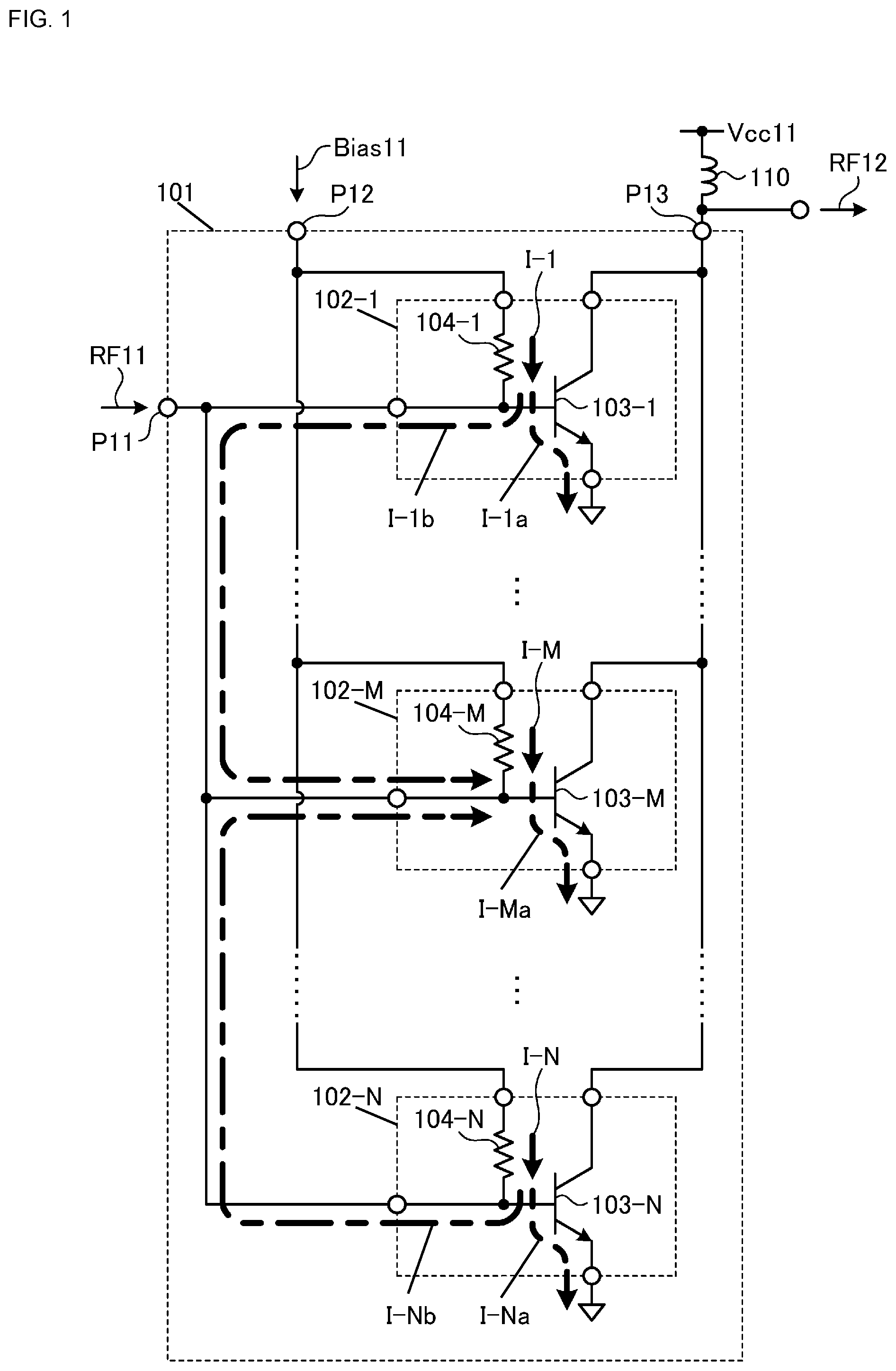
is a diagram illustrating the configuration of a multi-finger transistor 101 according to the comparative example. The multi-finger transistor 101 includes a plurality of unit transistors electrically connected in parallel to each other. Each unit transistor is a minimum element of the transistor.
The multi-finger transistor 101 includes a first terminal P 11 that receives an alternating current (AC) signal RF 11 , a second terminal P 12 that receives a bias current Bias 11 , and a third terminal P 13 that outputs an AC signal RF 12 . The third terminal P 13 is electrically connected to a power supply potential Vcc 11 via a choke inductor 110 .
The multi-finger transistor 101 receives power supplied from the power supply potential Vcc 11 and is brought into an electric bias state by the bias current Bias 11 . The multi-finger transistor 101 amplifies the AC signal RF 11 and outputs the amplified AC signal RF 12 .
The multi-finger transistor 101 includes N cells 102 - 1 to 102 -N. N is an integer greater than or equal to 2. The cell 102 - 1 includes a unit transistor 103 - 1 and a resistor 104 - 1 . The cell 102 -M includes a unit transistor 103 -M and a resistor 104 -M. M is an integer greater than 1 and smaller than N. The cell 102 -N includes a unit transistor 103 -N and a resistor 104 -N. The resistors 104 - 1 to 104 -N, each has a resistance value of, for example, about 180Ω to 200Ω. Note that the present disclosure is not limited thereto.
In the present disclosure, a unit transistor is a bipolar transistor, but the present disclosure is not limited thereto. The bipolar transistor may be a heterojunction bipolar transistor (HBT), but the present disclosure is not limited thereto. The unit transistor may be, for example, a field-effect transistor (FET).
The emitter or source of each unit transistor corresponds to an example of a “first terminal” of the present disclosure. The base or gate of each unit transistor corresponds to an example of a “second terminal” of the present disclosure. The collector or drain of each unit transistor corresponds to an example of a “third terminal” of the present disclosure.
The emitter of each unit transistor 103 is electrically connected to a reference potential. The reference potential may be a ground potential, but the present disclosure is not limited thereto. The base of each unit transistor 103 is electrically connected to the first terminal P 11 . One end of each resistor 104 is electrically connected to the second terminal P 12 . The other end of each resistor 104 is electrically connected to the base of the corresponding unit transistor 103 . The collector of each unit transistor 103 is electrically connected to the third terminal P 13 .
It is assumed that the AC signal RF 11 does not contain a direct current (DC) component but contains only an AC component. Thus, each cell 102 does not need to include a DC cut capacitor in the path between the first terminal P 11 and the base of the corresponding unit transistor 103 .
A current I- 1 flows through the resistor 104 - 1 . A current I-M flows through the resistor 104 -M. A current I-N flows through the resistor 104 -N. The sum of the currents I- 1 to I-N is equal to the bias current Bias 11 .
If the individual unit transistors 103 have the same electric characteristics, all the current I- 1 flows through a base-emitter path of the unit transistor 103 - 1 , all the current I-M flows through a base-emitter path of the unit transistor 103 -M, and all the current I-N flows through a base-emitter path of the unit transistor 103 -N.
However, for example, a difference in temperature between the unit transistors 103 may cause a difference in input impedance (input resistance) between the bases of the unit transistors 103 . Also, for example, an individual difference between the unit transistors 103 may cause a difference in input impedance between the bases of the unit transistors 103 .
Here, it is assumed that the input impedance of the unit transistor 103 -M is lower than the input impedances of the other unit transistors 103 , in other words, the unit transistor 103 -M has the lowest input impedance.
In this case, a part of the current I- 1 flows, as a current I- 1 a , through the base-emitter path of the unit transistor 103 - 1 , whereas the other part of the current I- 1 flows, as a current I- 1 b , through the base-emitter path of the unit transistor 103 -M. Likewise, a part of the current I-N flows, as a current I-Na, through the base-emitter path of the unit transistor 103 -N, whereas the other part of the current I-N flows, as a current I-Nb, through the base-emitter path of the unit transistor 103 -M.
Thus, a current I-Ma flowing through the base-emitter path of the unit transistor 103 -M is the sum of the current I-M and the currents flowing thereinto from the other cells. This causes a large bias current to flow through the base-emitter path of the unit transistor 103 -M and causes a small bias current to flow through the base-emitter paths of the other unit transistors 103 . This results in uneven operation of the plurality of unit transistors 103 . The uneven operation of the plurality of unit transistors 103 hinders a desired amplification characteristic from being obtained.
First Embodiment
is a diagram illustrating the configuration of a multi-finger transistor 1 according to the first embodiment. The multi-finger transistor 1 includes a plurality of unit transistors electrically connected in parallel to each other. Each unit transistor is a minimum element of the transistor.
The multi-finger transistor 1 includes a first terminal P 1 that receives an AC signal RF 1 , a second terminal P 2 that receives a bias current Bias 1 , and a third terminal P 3 that outputs an AC signal RF 2 . The third terminal P 3 is electrically connected to a power supply potential Vcc 1 via a choke inductor 10 .
The first terminal P 1 corresponds to an example of a “common input terminal” of the present disclosure. The second terminal P 2 corresponds to an example of a “common bias terminal” of the present disclosure. The third terminal P 3 corresponds to an example of a “common output terminal” of the present disclosure.
The multi-finger transistor 1 receives power supplied from the power supply potential Vcc 1 and is brought into an electric bias state by the bias current Bias 1 . The multi-finger transistor 1 amplifies the AC signal RF 1 and outputs the amplified AC signal RF 2 .
The multi-finger transistor 1 includes N cells 2 - 1 to 2 -N. The cell 2 - 1 includes a unit transistor 3 - 1 , a resistor 4 - 1 , and a resistor 5 - 1 . The cell 2 -M includes a unit transistor 3 -M, a resistor 4 -M, and a resistor 5 -M. The cell 2 -N includes a unit transistor 3 -N, a resistor 4 -N, and a resistor 5 -N. The resistors 4 - 1 to 4 -N, each has a resistance value of, for example, about 180Ω to 200Ω. Note that the present disclosure is not limited thereto. The resistors 5 - 1 to 5 -N, each has a resistance value of, for example, about 1Ω. Note that the present disclosure is not limited thereto. The resistors 5 - 1 to 5 -N, each has, for example, a smaller resistance value than the resistance value of a corresponding one of the resistors 4 - 1 to 4 -N. Note that the present disclosure is not limited thereto. The resistors 4 - 1 to 4 -N, each has, for example, a resistance value that is five times or more the resistance value of a corresponding one of the resistors 5 - 1 to 5 -N. Note that the present disclosure is not limited thereto.
The resistors 5 correspond to an example of “first resistance elements” of the present disclosure. The resistors 4 correspond to an example of “second resistance elements” of the present disclosure.
The emitter of each unit transistor 3 is electrically connected to a reference potential. One end of each resistor 5 is electrically connected to the base of the corresponding unit transistor 3 . The other end of each resistor 5 is electrically connected to the first terminal P 1 . One end of each resistor 4 is electrically connected to the base of the corresponding unit transistor 3 . The other end of each resistor 4 is electrically connected to the second terminal P 2 . The collector of each unit transistor 3 is electrically connected to the third terminal P 3 .
The AC signal RF 1 contains only an AC component. Thus, each cell 2 does not need to include a DC cut capacitor in the path between the first terminal P 1 and the base of the corresponding unit transistor 3 .
A current I- 1 flows through the resistor 4 - 1 . A current I-M flows through the resistor 4 -M. A current I-N flows through the resistor 4 -N. The sum of the currents I- 1 to I-N is equal to the bias current Bias 1 .
For example, a difference in temperature between the unit transistors 3 may cause a difference in input impedance (input resistance) between the bases of the unit transistors 3 . Also, for example, an individual difference between the unit transistors 3 may cause a difference in input impedance between the bases of the unit transistors 3 .
Here, it is assumed that the input impedance of the unit transistor 3 -M is lower than the input impedances of the other unit transistors 3 , in other words, the unit transistor 3 -M has the lowest input impedance.
However, the one end of each resistor 4 is electrically connected to the base of the corresponding unit transistor 3 and is also electrically connected to the one end of the corresponding resistor 5 .
The presence of the resistor 5 - 1 hinders the current I- 1 flowing through the resistor 4 - 1 from flowing toward the resistor 5 - 1 , and thus the current I- 1 becomes a current I- 1 a flowing through a base-emitter path of the unit transistor 3 - 1 . Likewise, the presence of the resistor 5 -M hinders the current I-M flowing through the resistor 4 -M from flowing toward the resistor 5 -M, and thus the current I-M becomes a current I-Ma flowing through a base-emitter path of the unit transistor 3 -M. Likewise, the presence of the resistor 5 -N hinders the current I-N flowing through the resistor 4 -N from flowing toward the resistor 5 -N, and thus the current I-N becomes a current I-Na flowing through a base-emitter path of the unit transistor 3 -N.
Accordingly, uneven operation of the unit transistors 3 is suppressed, and thus a desired amplification characteristic is obtained.
Each resistor 5 will be illustrated below, but the present disclosure is not limited thereto.
When a multi-finer transistor is regarded as a single transistor, a combined resistance of each resistor 5 is, for example, about 0.5Ω or more. Thus, the resistance value of the resistors 5 connected to the unit transistors is, when the number of unit transistors is N, for example, about (0.5×N)Ω or more.
The resistance value of each resistor 5 is, for example, smaller than the resistance value of an emitter ballast resistor of the corresponding unit transistor 3 . The emitter ballast resistor has, for example, about 200Ω, but the present disclosure is not limited thereto.
The resistance value of each resistor 5 is, for example, a resistance value corresponding to the impedance of a DC cut capacitor that is typically connected to the base of the corresponding unit transistor 3 , but the present disclosure is not limited thereto. For example, it is typically assumed that, when the AC signal RF 1 has a frequency in the band of about 0.9 GHz, a DC cut capacitor of about 2 pF is connected in series to the base of each unit transistor 3 . In this case, the resistance value corresponding to an impedance of about (1/ωC) of the DC cut capacitor is about 88Ω.
Second Embodiment
is a diagram illustrating the configuration of a power amplifier circuit 11 according to a second embodiment. Specifically, is a diagram illustrating the configuration of the power amplifier circuit 11 to which the multi-finger transistor 1 according to the first embodiment is applied.
The power amplifier circuit 11 may be implemented by a hybrid integrated circuit (IC) or module in which a plurality of components (semiconductor chips or the like) are mounted on a single substrate, but the present disclosure is not limited thereto.
The power amplifier circuit 11 includes a multi-finger transistor 12 serving as a first-stage power amplifier, multi-finger transistors 13 and 14 serving as second-stage power amplifiers, and multi-finger transistors 15 and 16 serving as third-stage power amplifiers. The number of stages of the power amplifiers is not limited to three, and may be two or less, or may be four or more.
The multi-finger transistor 12 is a typical multi-finger transistor in which a DC cut capacitor is connected in series to the base thereof. The multi-finger transistors 13 to 16 , each has the same circuit configuration as that of the multi-finger transistor 1 according to the first embodiment (see ).
The multi-finger transistor 12 includes cells each including a unit transistor 12 a , a DC cut capacitor 12 b , and a resistor 12 c.
The emitter of the unit transistor 12 a of each cell of the multi-finer transistor 12 is electrically connected to a reference potential. A radio-frequency (RF) input signal RFin is input to the base of the unit transistor 12 a of each cell via the DC cut capacitor 12 b of the cell. A bias current Bias 21 is input to the base of the unit transistor 12 a of each cell via the resistor 12 c of the cell. The collector of the unit transistor 12 a of each cell is electrically connected to a power supply potential Vcc 21 via a choke inductor 31 . The unit transistor 12 a of each cell outputs an RF signal RF 21 from the collector to one end of a primary winding of a balun T 1 via a DC cut capacitor 32 .
The other end of the primary winding of the balun T 1 is electrically connected to the reference potential. An RF signal RF 22 is output from one end of a secondary winding of the balun T 1 to the base of the multi-finger transistor 13 . An RF signal RF 23 is output from the other end of the secondary winding of the balun T 1 to the base of the multi-finger transistor 14 .
The multi-finger transistor 13 includes cells each including a unit transistor 13 a and resistors 13 b and 13 c.
The emitter of the unit transistor 13 a of each cell of the multi-finer transistor 13 is electrically connected to the reference potential. The RF signal RF 22 is input to the base of the unit transistor 13 a of each cell via the resistor 13 b of the cell.
The RF signal RF 22 output from the secondary winding of the balun T 1 does not contain a DC component, and thus a DC cut capacitor is optional between the secondary winding of the balun T 1 and the base of the unit transistor 13 a of each cell.
A bias current Bias 22 is input to the base of the unit transistor 13 a of each cell via the resistor 13 c of the cell. The collector of the unit transistor 13 a of each cell is electrically connected to one end of a primary winding of a balun T 2 . The unit transistor 13 a of each cell outputs an RF signal RF 24 from the collector to the one end of the primary winding of the balun T 2 .
The multi-finger transistor 14 includes cells each including a unit transistor 14 a and resistors 14 b and 14 c.
The emitter of the unit transistor 14 a of each cell of the multi-finer transistor 14 is electrically connected to the reference potential. The RF signal RF 23 is input to the base of the unit transistor 14 a of each cell via the resistor 14 b of the cell.
The RF signal RF 23 output from the secondary winding of the balun T 1 does not contain a DC component, and thus a DC cut capacitor is optional between the secondary winding of the balun T 1 and the base of the unit transistor 14 a of each cell.
A bias current Bias 23 is input to the base of the unit transistor 14 a of each cell via the resistor 14 c of the cell. The collector of the unit transistor 14 a of each cell is electrically connected to the other end of the primary winding of the balun T 2 . The unit transistor 14 a of each cell outputs an RF signal RF 25 from the collector to the other end of the primary winding of the balun T 2 .
The midpoint of the primary winding of the balun T 2 is electrically connected to a power supply potential Vcc 22 . The power supply potential Vcc 22 is supplied to the collectors of the multi-finger transistors 13 and 14 via the primary winding of the balun T 2 .
An RF signal RF 26 is output from one end of a secondary winding of the balun T 2 to the base of the multi-finger transistor 15 . An RF signal RF 27 is output from the other end of the secondary winding of the balun T 2 to the base of the multi-finger transistor 16 .
The multi-finger transistor 15 includes cells each including a unit transistor 15 a and resistors 15 b and 15 c.
The emitter of the unit transistor 15 a of each cell of the multi-finer transistor 15 is electrically connected to the reference potential. The RF signal RF 26 is input to the base of the unit transistor 15 a of each cell via the resistor 15 b of the cell.
The RF signal RF 26 output from the secondary winding of the balun T 2 does not contain a DC component, and thus a DC cut capacitor is optional between the secondary winding of the balun T 2 and the base of the unit transistor 15 a of each cell.
A bias current Bias 24 is input to the base of the unit transistor 15 a of each cell via the resistor 15 c of the cell. The collector of the unit transistor 15 a of each cell is electrically connected to one end of a primary winding of a balun T 3 . The unit transistor 15 a of each cell outputs an RF signal RF 28 from the collector to the one end of the primary winding of the balun T 3 .
The multi-finger transistor 16 includes cells each including a unit transistor 16 a and resistors 16 b and 16 c.
The emitter of the unit transistor 16 a of each cell of the multi-finer transistor 16 is electrically connected to the reference potential. The RF signal RF 27 is input to the base of the unit transistor 16 a of each cell via the resistor 16 b of the cell.
The RF signal RF 27 output from the secondary winding of the balun T 2 does not contain a DC component, and thus a DC cut capacitor is optional between the secondary winding of the balun T 2 and the base of the unit transistor 16 a of each cell.
A bias current Bias 25 is input to the base of the unit transistor 16 a of each cell via the resistor 16 c of the cell. The collector of the unit transistor 16 a of each cell is electrically connected to the other end of the primary winding of the balun T 3 . The unit transistor 16 a of each cell outputs an RF signal RF 29 from the collector to the other end of the primary winding of the balun T 3 .
The midpoint of the primary winding of the balun T 3 is electrically connected to a power supply potential Vcc 23 . The power supply potential Vcc 23 is supplied to the collectors of the multi-finger transistors 15 and 16 via the primary winding of the balun T 3 .
One end of a secondary winding of the balun T 3 is electrically connected to the reference potential. An RF output signal RFout is output from the other end of the secondary winding of the balun T 3 .
With this configuration, the power amplifier circuit 11 does not have a DC cut capacitance in each of the intermediate stage and the output stage, and thus a filter effect, which is based on a time constant determined by the product of the resistances connected to the bias circuit (for example, the resistors 13 c , 14 c , 15 c , and 16 c ) and the capacitance, is not obtained. Thus, there is no limitation on the band resulting from a modulation band width.
While embodiments of the disclosure have been described above, it is to be understood that variations, modifications, and improvements will be apparent to those skilled in the art without necessarily departing from the scope and spirit of the disclosure. The embodiments are for facilitating the understanding of the present disclosure and are not intended to limit the present disclosure. The present disclosure includes the equivalents thereof. The scope of the disclosure, therefore, is to be determined solely by the following claims.
Figures (3)
Citations
This patent cites (18)
- US5867061
- US7190219
- US7486141
- US7961048
- US8130041
- US8547174
- US8917145
- US9705451
- US11671061
- US2004/0145402
- US2007/0152751
- US2009/0231033
- US2010/0148877
- US2012/0200359
- US2015/0054581
- US2015/0180423
- US2016/0056769
- US2015/001851