Abstract
A directional coupler splits an input signal received by an input terminal into four signals to be output to output terminals. The directional coupler includes couplers and phase shifters. The coupler is connected to the input terminal and splits the input signal into two signals to be output to terminals. The coupler splits a signal from the terminal into two signals to be output to the output terminals. The coupler splits a signal from the terminal into two signals to be output to the output terminals. The phase shifter is connected between the terminal and the coupler and advances the phase of the signal from the terminal. The phase shifter is connected between the terminal and the coupler and delays the phase of the signal from the terminal. The phase difference between output signals of the phase shifters is 180°±10°.
Claims (12)
1. A directional coupler configured to split an input signal into four output signals, the directional coupler comprising: an input terminal configured to receive the input signal; first, second, third, and fourth output terminals; a first coupler that is connected to the input terminal, and that is configured to split the input signal into two signals that are respectively output to a first terminal and a second terminal; a second coupler configured to split a signal from the first terminal into two signals that are respectively output to the first output terminal and the second output terminal; a third coupler configured to split a signal from the second terminal into two signals that are respectively output to the third output terminal and the fourth output terminal; a first phase shifter that is connected between the first terminal and the second coupler, and that is configured to advance a phase of the signal from the first terminal; and a second phase shifter that is connected between the second terminal and the third coupler, and that is configured to delay a phase of the signal from the second terminal, wherein a phase difference between a signal output from the first phase shifter and a signal output from the second phase shifter is 180°±10°.
Show 11 dependent claims
2. The directional coupler according to claim 1 , wherein a phase of a signal output from the first output terminal is 0°, wherein a phase of a signal output from the second output terminal is 90°±10° relative to the signal output from the first output terminal, wherein a phase of a signal output from the third output terminal is 180°±10° relative to the signal output from the first output terminal, and wherein a phase of a signal output from the fourth output terminal is 270°±10° relative to the signal output from the first output terminal.
3. The directional coupler according to claim 1 , wherein the first phase shifter is a high-pass filter; and wherein the second phase shifter is a low-pass filter.
4. The directional coupler according to claim 3 , wherein the first phase shifter and the second phase shifter are each an LC filter with a T-type structure or a n-type structure.
5. The directional coupler according to claim 1 , further comprising: a dielectric substrate, wherein the first phase shifter, the second phase shifter, and the first, second, and third couplers are on the dielectric substrate.
6. The directional coupler according to claim 5 , wherein in plan view of the dielectric substrate from a normal direction of the dielectric substrate: the first phase shifter is between the first coupler and the second coupler, and the second phase shifter is between the first coupler and the third coupler.
7. The directional coupler according to claim 6 , wherein in plan view of the dielectric substrate from the normal direction of the dielectric substrate: the first coupler, the first phase shifter, and the second coupler are arranged in a first direction, and the first coupler, the second phase shifter, and the third coupler are arranged in the first direction.
8. The directional coupler according to claim 6 , wherein in plan view of the dielectric substrate from the normal direction of the normal direction: the first coupler, the first phase shifter, and the second coupler are arranged in a first direction, and the first coupler, the second phase shifter, and the third coupler are arranged in a second direction different from the first direction.
9. The directional coupler according to claim 1 , further comprising: a dielectric substrate with a multilayer structure, wherein the first coupler is in a first part of the dielectric substrate, wherein the second coupler is in a second part that is different from the first part in a stacking direction of the dielectric substrate, wherein the third coupler is in a third part that is different from the first part in the stacking direction of the dielectric substrate, wherein the first phase shifter is in a fourth part located between the first part and the second part, and wherein the second phase shifter is in a fifth part located between the first part and the third part.
10. The directional coupler according to claim 9 , wherein the second part and the third part are located in a same position in the stacking direction of the dielectric substrate.
11. The directional coupler according to claim 9 , wherein the dielectric substrate comprises a ground electrode in each of a layer between the first part and the fourth part, a layer between the first part and the fifth part, a layer between the second part and the fourth part, and a layer between the third part and the fifth part.
12. The directional coupler according to claim 9 , wherein the first phase shifter is an LC filter comprising a capacitor and an inductor, and wherein a permittivity of the fourth part of the dielectric substrate is greater than a permittivity of the first part, the second part, and the third part of the dielectric substrate.
Full Description
Show full text →
CROSS REFERENCE TO RELATED APPLICATION
This is a continuation of International Application No. PCT/JP2021/042769 filed on Nov. 22, 2021 which claims priority from Japanese Patent Application No. 2021-013087 filed on Jan. 29, 2021. The contents of these applications are incorporated herein by reference in their entireties.
BACKGROUND ART
Technical Field
This disclosure relates to a directional coupler and, more particularly, relates to a technology for stabilizing phases between output signals in a four-way coupler.
Japanese Unexamined Patent Application Publication No. 10-145103 (Patent Document 1) discloses a four-phase converter (directional coupler) that outputs an input signal as four signals that are out of phase with each other by 90°.
The four-phase converter disclosed in Patent Document 1 includes a two-wire 90-degree coupler connected to an input terminal and two 180-degree baluns connected, respectively, to the two outputs of the 90-degree coupler. In the four-phase converter disclosed in Patent Document 1, four output signals, which are out of phase with each other by 90°, are output from four output terminals.
•
• Patent Document 1: Japanese Unexamined Patent Application Publication No. 10-145103
BRIEF SUMMARY
In a communication device that transmits and receives radio frequency signals, an array antenna including multiple radiating elements may be used. In such a communication device, a directional coupler as described above may be used to distribute one signal to the multiple radiating elements.
Along with the growing need for a broadband and low-loss communication device, there is a demand for a low-loss directional coupler that can stabilize the phase differences between output signals across a wide frequency band.
This disclosure provides a low-loss four-way directional coupler that can stabilize the phase differences between output signals across a wide frequency band.
A directional coupler according to this disclosure splits an input signal received by an input terminal into four signals to be output to first through fourth output terminals. The directional coupler includes first through third couplers and first and second phase shifters. The first coupler is connected to the input terminal and splits the input signal into two signals to be output to a first terminal and a second terminal. The second coupler splits a signal from the first terminal into two signals to be output to the first output terminal and the second output terminal. The third coupler splits a signal from the second terminal into two signals to be output to the third output terminal and the fourth output terminal. The first phase shifter is connected between the first terminal and the second coupler and advances the phase of the signal from the first terminal. The second phase shifter is connected between the second terminal and the third coupler and delays the phase of the signal from the second terminal. The phase difference between the signal output from the first phase shifter and the signal output from the second phase shifter is 180°±10°.
A directional coupler according to this disclosure has a configuration in which one of output signals of a first coupler connected to an input terminal is provided via a first phase shifter to a second coupler, and the other one of the output signals is provided via a second phase shifter to a third coupler. The two phase shifters are designed such that the phase difference between the output signals is 180°±10°. This configuration in which the phase shifters are disposed in the middle makes it possible to adjust the frequency characteristics of the phase difference between signals input to the second coupler and the third coupler within a desired range. This in turn makes it possible to provide a low-loss four-way directional coupler that can stabilize the phase differences between output signals across a wide frequency band.
BRIEF DESCRIPTION OF THE DRAWINGS
is a circuit diagram of a directional coupler according to an embodiment.
A and 2 B are drawings illustrating variations of a phase shifter.
is a drawing for describing the characteristics of the directional coupler in .
is a graph for describing the frequency characteristics of phase shifters.
is an exterior perspective view of the directional coupler in .
A is a drawing illustrating an example of an arrangement of elements of the directional coupler in .
B is a drawing illustrating an example of an arrangement of elements of a directional coupler according to a variation.
is an exploded perspective view of an example of a multilayer structure of the directional coupler in .
is a drawing illustrating a first example of a directional coupler with a two-dimensional configuration.
is a drawing illustrating a second example of a directional coupler with a two-dimensional configuration.
is a drawing illustrating a third example of a directional coupler with a two-dimensional configuration.
DETAILED DESCRIPTION
An embodiment of this disclosure is described in detail below with reference to the drawings. The same reference number is assigned to the same or similar components in the drawings, and the descriptions of those components are not repeated.
[Configuration of Directional Coupler]
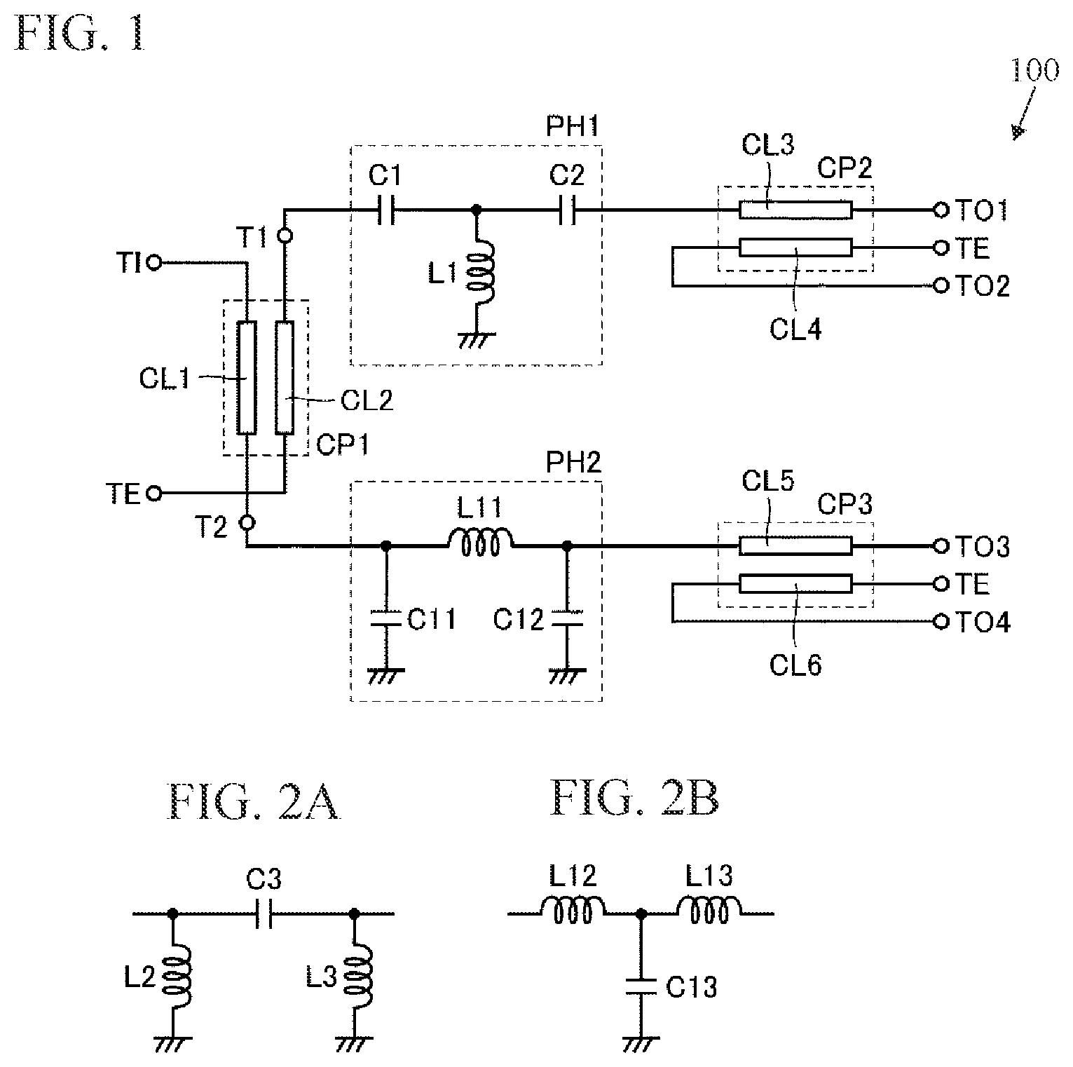
is a circuit diagram of a directional coupler 100 according to an embodiment. Referring to , the directional coupler 100 includes couplers CP 1 , CP 2 , and CP 3 and phase shifters PH 1 and PH 2 . The directional coupler 100 splits a signal received at an input terminal TI into four signals and outputs the four signals from output terminals 101 through 104 . The phase shifter PH 1 is connected between the coupler CP 1 and the coupler CP 2 . The phase shifter PH 2 is connected between the coupler CP 1 and the coupler CP 3 .
Each of the couplers CP 1 through CP 3 is a two-wire coupler that includes two parallel lines, splits an input signal into two signals, and outputs the two signals. When the wavelength of a radio frequency signal to be transmitted is λ, each line of each coupler has an electrical length of λ/4. In each coupler, when a signal flows through one of the lines, a signal is induced in another one of the lines due to electromagnetic field coupling.
The coupler CP 1 includes a first line CL 1 and a second line CL 2 that are disposed parallel to each other. In the coupler CP 1 , one end of the first line CL 1 is connected to the input terminal TI, and another end of the first line CL 1 is connected to a second terminal on the output side. An end of the second line CL 2 facing the end of the first line CL 1 closer to the second terminal T 2 is connected to an end terminal TE. An end of the second line CL 2 facing the end of the first line CL 1 closer to the input terminal TI is connected to a first terminal T 1 . The impedance of the end terminal TE is set at a characteristic impedance of 50Ω. The first terminal T 1 of the coupler CP 1 is connected to the phase shifter PH 1 .
The phase shifter PH 1 is an LC filter including capacitors C 1 and C 2 and an inductor L 1 . The capacitors C 1 and C 2 are connected in series between the coupler CP 1 and the coupler CP 2 . The inductor L 1 is connected between a connection node between the capacitor C 1 and the capacitor C 2 and the ground potential. That is, the phase shifter PH 1 constitutes a so-called T-type high-pass filter.
Accordingly, the phase of an output signal of the phase shifter PH 1 is advanced relative to an input signal of the phase shifter PH 1 .
The coupler CP 2 includes a third line CL 3 and a fourth line CL 4 that are disposed parallel to each other. One end of the third line CL 3 is connected to the phase shifter PH 1 , and another end of the third line CL 3 is connected to an output terminal TO 1 . An end of the fourth line CL 4 facing the end of the third line CL 3 closer to the phase shifter PH 1 is connected to an output terminal TO 2 . An end of the fourth line CL 4 facing the end of the third line CL 3 closer to the output terminal TO 1 is connected to an end terminal TE.
The phase shifter PH 2 is an LC filter including capacitors C 11 and C 12 and an inductor L 11 . The capacitor C 11 is connected between an end of the inductor L 11 closer to the coupler CP 1 and the ground potential. The capacitor C 12 is connected between an end of the inductor L 11 closer to the coupler CP 3 and the ground potential. That is, the phase shifter PH 2 constitutes a so-called n-type low-pass filter. Accordingly, the phase of an output signal of the phase shifter PH 2 is delayed relative to an input signal of the phase shifter PH 2 . In the directional coupler 100 of the embodiment, the phase shifter PH 1 is adjusted such that the phase of the phase shifter PH 1 is advanced by 90° relative to the phase shifter PH 2 .
The coupler CP 3 includes a fifth line CL 5 and a sixth line CL 6 that are disposed parallel to each other. One end of the fifth line CL 5 is connected to the phase shifter PH 2 , and another end of the fifth line CL 5 is connected to an output terminal TO 3 . An end of the sixth line CL 6 facing the end of the fifth line CL 5 closer to the phase shifter PH 2 is connected to an output terminal TO 4 . An end of the sixth line CL 6 facing the end of the fifth line CL 5 closer to the output terminal TO 3 is connected to an end terminal TE.
The configurations of the phase shifters PH 1 and PH 2 are not limited to the configurations described above as long as the phase of the phase shifter PH 1 is advanced by 90° relative to the phase of the phase shifter PH 2 . For example, the phase shifter PH 1 may also be configured as a so-called n-type high-pass filter as illustrated in A in which one ends of inductors L 2 and L 3 are connected to the corresponding ends of a capacitor C 3 and other ends of the inductors L 2 and L 3 are grounded. The phase shifter PH 2 may also be configured as a so-called T-type low-pass filter as illustrated in B in which one end of a capacitor C 13 is grounded, and another end of the capacitor C 13 is connected to a connection node between inductors L 12 and L 13 that are connected in series.
In the directional coupler 100 with a circuit configuration as described above, when a radio frequency signal is supplied to the input terminal TI, an electric current flows through the first line CL 1 from the input terminal TI toward the second terminal T 2 . As described above, when a signal flows through the first line CL 1 , a signal is induced in the second line CL 2 due to electromagnetic field coupling.
Because the end of the second line CL 2 facing the end of the first line CL 1 closer to the second terminal T 2 is connected to the end terminal TE and the electrical length of each of the lines is λ/4, the phase of the signal induced in the second line CL 2 and output from the first terminal T 1 is advanced by 90° relative to the signal output from the second terminal T 2 . Similarly, in the coupler CP 2 , the phase of a signal output from the output terminal TO 2 is advanced by 90° relative to the phase of a signal output from the output terminal TO 1 . Also, in the coupler CP 3 , a signal output from the output terminal TO 4 is advanced by 90° relative to the phase of a signal output from the output terminal TO 3 .
Here, in a configuration in which the phase shifters PH 1 and PH 2 are not provided, when the phase of a signal output by the coupler CP 2 from the output terminal TO 1 is 0°, a signal with a phase of +90° is output from the output terminal TO 2 . On the other hand, because a signal with a phase delayed by 90° from the signal input to the coupler CP 2 is input to the coupler CP 3 from the coupler CP 1 , a signal with a phase of −90° (i.e., +270°) relative to the signal output from the output terminal TO 1 is output from the output terminal TO 3 , and a signal with a phase of 0° is output from the output terminal TO 4 . Accordingly, the signal output from the output terminal TO 1 is in phase with the signal output from the output terminal TO 4 . As a result, for example, in an antenna in which separate radiating elements are connected to respective output terminals, a radio wave from the radiating element connected to the output terminal TO 1 may interfere with a radio wave from the radiating element connected to the output terminal TO 4 .
In contrast, in the directional coupler 100 of the embodiment, because the phase shifter PH 1 is adjusted such that the phase of the phase shifter PH 1 is advanced by 90° relative to the phase shifter PH 2 , the phase of a signal output from the phase shifter PH 1 advances almost 180° in total relative to the phase of a signal output from the phase shifter PH 2 . With this configuration, when the phase of a signal output from the output terminal TO 1 is 0°, a signal with a phase of +90° is output from the output terminal TO 2 . On the other hand, in the coupler CP 3 , a signal with a phase of −180° (i.e., +180°) is output from the output terminal TO 3 , and a signal with a phase of −90° (i.e., +270°) is output from the output terminal TO 4 . Thus, in the directional coupler 100 , signals that are out of phase with each other by 90° are output from the output terminals TO 1 through TO 4 . This configuration makes it possible to prevent the radio wave interference between radiating elements in an antenna in which separate radiating elements are connected to respective output terminals. The phase difference between a signal output from the phase shifter PH 1 and a signal output from the phase shifter PH 2 does not have to be exactly 180°, and a phase difference of 180°±10° is tolerable. Also, variations of the phase differences between signals output from the output terminals TO 1 through TO 4 within a range of ±10° are tolerable.
A directional coupler is used in a communication device for transmitting and receiving radio frequency signals to distribute one signal to multiple paths. Meanwhile, there has been a high need for a broadband and low-loss communication device, and this need is particularly growing along with the spread of the 5th generation communication standard (5G).
In a directional coupler, output signals generally have frequency characteristics, and the phases of the output signals may change relative to input signals along with a frequency change. Here, when phase-frequency characteristics of the output signals differ from each other, the phase differences between the output signals may vary, and it may become difficult to achieve desired gain or loss characteristics.
In the four-way directional coupler of the present embodiment, as described above, a phase shifter is provided in each of paths between an input-side coupler and two output-side couplers. The phase shifters make it possible to properly adjust the phase difference between input signals input to the two output-side couplers. This in turn makes it possible to stabilize the phase differences between output signals in a desired pass band.
[Characteristics of Directional Coupler]
is a drawing for describing the characteristics of the directional coupler 100 illustrated in . In , the left graph shows the total loss of signals output from all output terminals with respect to an input signal, and the middle graph shows an insertion loss for each of the output terminals. Also, the right graph in shows the phases of signals output from the output terminals.
In each graph in , the horizontal axis indicates a frequency. The frequency band between F 1 and F 2 in each graph is a desired pass band BW 1 . Also, in “insertion loss” (middle graph) and “phase” (right graph), solid lines LN 11 and LN 21 indicate the output terminal TO 1 , dotted lines LN 12 and LN 22 indicate the output terminal TO 4 , dashed-dotted lines LN 13 and LN 23 indicate the output terminal TO 3 , and dashed-two dotted lines LN 14 and LN 24 indicate the output terminal TO 2 .
Referring first to “total loss” (left graph) in , within the range of the pass band BW 1 , the loss is about 1.0 to 1.2 dB (solid line LN 1 ), and low-loss and almost flat characteristics are observed across the entire pass band BW 1 .
The insertion loss (middle graph) of each of the output terminals is 6 to 8 dB in the pass band BW 1 , and the output levels of the output signals are substantially the same across the entire pass band BW 1 . In the pass band BW 1 , the phase (right graph) of each output signal changes in the delay direction as the frequency increases. However, the slopes of change of the output signals are substantially the same, and the phase differences between the output signals are substantially constant regardless of the frequency.
That is, the directional coupler 100 has such characteristics that across a desired pass band, the loss is low and the phase differences between output signals are substantially constant.
is a graph for describing the frequency characteristics of the phase shifter PH 1 and the phase shifter PH 2 . In , a solid line LN 31 indicates the phase of an output signal of the phase shifter PH 1 , and a dotted line LN 32 indicates the phase of an output signal of the phase shifter PH 1 . Also, a solid line LN 30 indicates the phase difference between the output signals of the phase shifter PH 1 and the phase shifter PH 2 .
Referring to , in the pass band BW 1 , the phase of each of the phase shifters PH 1 and PH 2 changes in the delay direction as the frequency increases. However, the phase difference between the phase shifters PH 1 and PH 2 is substantially constant at about 90° across the entire pass band BW 1 . Thus, by designing the phase shifters such that the phase difference between the phase shifters PH 1 and PH 2 becomes substantially 90° in a desired pass band, it is possible to achieve low loss and stabilize the phase differences between output signals in the desired pass band.
[Detailed Configurations of Directional Couplers]
Next, detailed configurations of directional couplers are described with reference to through 10 . through 7 illustrate examples in which elements constituting a directional coupler are three-dimensionally arranged on a substrate. through 10 illustrate examples in which elements are two-dimensionally arranged on a substrate.
Examples of Three-Dimensional Configurations
is an exterior perspective view of the directional coupler 100 . Referring to , the directional coupler 100 includes a dielectric substrate 110 that has a multilayer structure and has a cuboid or substantially cuboid shape. As described later with reference to , the dielectric substrate 110 is formed by stacking multiple dielectric layers LY 1 through LY 21 in a predetermined direction. In the dielectric substrate 110 , the direction in which the multiple dielectric layers LY 1 through LY 21 are stacked is referred to as a stacking direction. Each dielectric layer of the dielectric substrate 110 is formed of a ceramic such as low temperature co-fired ceramics (LTCC) or a resin. In the dielectric substrate 110 , inductors and capacitors constituting the couplers CP 1 through CP 3 and the phase shifters PH 1 and PH 2 are implemented by multiple electrodes provided in the dielectric layers and multiple vias provided between the dielectric layers. In the present application, “via” indicates a conductor provided in a dielectric layer(s) to connect electrodes provided in different dielectric layers. A via may be formed of, for example, a conductive paste, plating, and/or a metal pin.
In the descriptions below, the stacking direction of the dielectric substrate 110 is referred to as a “Z-axis direction”, a direction that is perpendicular to the Z-axis direction and along the long side of the dielectric substrate 110 is referred to as an “X-axis direction”, and a direction along the short side of the dielectric substrate 110 is referred to as a “Y-axis direction”. Also, in the descriptions below, the positive and negative Z-axis directions in each drawing may be referred to as “upward” and “downward”, respectively.
A directional mark DM for identifying the orientation of the substrate is provided on an upper surface 111 of the dielectric substrate 110 . Also, the dielectric substrate 110 includes multiple external electrodes each of which has a substantially C-shape and extends from the upper surface 111 via the corresponding side surface of the dielectric substrate 110 to a lower surface 112 . The multiple external electrodes includes the input terminal TI, the output terminals TO 1 through TO 4 , the end terminals TE, and ground terminals GND. The dielectric substrate 110 is electrically connected to a mounting board (not shown) via parts of the external electrodes on the lower surface 112 by using connection parts such as solder.
A is a schematic diagram illustrating an example of an arrangement of elements of the directional coupler 100 illustrated in . B is a drawing illustrating an example of an arrangement of elements of a directional coupler 100 A according to a variation.
In the directional coupler 100 of the embodiment illustrated in A , the input-side coupler CP 1 is disposed in a first part RG 1 closer to the upper surface 111 of the dielectric substrate 110 . The output-side couplers CP 2 and CP 3 are disposed in a second part RG 2 and a third part RG 3 closer to the lower surface 112 of the dielectric substrate 110 , respectively. The phase shifter PH 1 is disposed in a fourth part RG 4 located between the coupler CP 1 and the coupler CP 2 in the stacking direction (the Z-axis direction) of the dielectric substrate 110 . The phase shifter PH 2 is disposed in a fifth part RG 5 located between the coupler CP 1 and the coupler CP 3 in the stacking direction of the dielectric substrate 110 . The fourth part RG 4 in which the phase shifter PH 1 is disposed may be in the same layer as the fifth part RG 5 in which the phase shifter PH 2 is disposed, or may be in a different layer from the fifth part RG 5 .
Elements of the directional coupler 100 A of the variation illustrated in B are arranged in the reverse order of the directional coupler 100 . That is, the input-side coupler CP 1 is disposed in a first part RG 1 A closer to the lower surface 112 of the dielectric substrate 110 . The output-side couplers CP 2 and CP 3 are disposed in a second part RG 2 A and a third part RG 3 A closer to the upper surface 111 of the dielectric substrate 110 , respectively. The phase shifter PH 1 is disposed in a fourth part RG 4 A located between the coupler CP 1 and the coupler CP 2 in the stacking direction of the dielectric substrate 110 . The phase shifter PH 2 is disposed in a fifth part RG 5 A located between the coupler CP 1 and the coupler CP 3 in the stacking direction of the dielectric substrate 110 .
In each of the directional couplers 100 and 100 A, couplers and phase shifters constituting the directional coupler are arranged and stacked in the Z-axis direction. With this configuration, although the size of the directional coupler in the Z-axis direction slightly increases, the area in plan view of the directional coupler from the Z axis direction decreases. Accordingly, compared with two-dimensional configurations described later with reference to through 10 , the area of the directional coupler occupied on the mounting board is smaller. Accordingly, it is possible to reduce the size of a circuit including the directional coupler.
is an exploded perspective view of an example of a multilayer structure of the directional coupler 100 in . As described above, the dielectric substrate 110 has a structure in which multiple dielectric layers LY 1 through LY 21 are stacked in the Z-axis direction.
The directional mark DM for identifying the orientation of the substrate is provided on the upper surface 111 (the dielectric layer LY 1 ) of the dielectric substrate 110 . The ground terminals GND are disposed on the short sides of the dielectric layer LY 1 ; and the input terminal TI, the output terminals TO 1 through TO 4 , and the end terminals TE are disposed on the long sides of the dielectric layer LY 1 . As illustrated in , each electrode extends via the corresponding side surface of the dielectric substrate 110 to the lower surface 112 (the dielectric layer LY 21 ).
Roughly speaking, the dielectric layers LY 3 through LY 6 (the first part RG 1 ) constitute the coupler CP 1 , and the dielectric layers LY 17 through LY 20 (the second part RG 2 and the third part RG 3 ) constitute the couplers CP 2 and CP 3 . The phase shifters PH 1 and PH 2 are provided in the dielectric layers LY 8 through LY 15 (the fourth part RG 4 and the fifth part RG 5 ). Planar electrodes GP 1 , GP 2 , GP 3 , and GP 4 connected to the ground terminals GND are disposed in the dielectric layer LY 2 , the dielectric layer LY 7 , the dielectric layer LY 16 , and the dielectric layer LY 21 , respectively. In other words, the planar electrode GP 2 is disposed between the first part RG 1 and the fourth and fifth parts RG 4 and RG 5 , and the planar electrode GP 3 is disposed between the second and third parts RG 2 and RG 3 and the fourth and fifth parts RG 4 and RG 5 .
The planar electrodes GP 1 and GP 4 are disposed close to the upper surface 111 and the lower surface 112 , respectively, and function as shields to reduce the influence of electromagnetic waves from the outside. The planar electrode GP 2 is disposed in a layer between the coupler CP 1 and the phase shifters PH 1 and PH 2 . The planar electrode GP 2 suppresses electromagnetic field coupling between the coupler CP 1 and each phase shifter. The planar electrode GP 3 suppresses electromagnetic field coupling between the coupler CP 2 and the phase shifter PH 1 and between the coupler CP 3 and the phase shifter PH 2 .
The input terminal TI is connected to a linear wiring electrode LP 1 disposed in the dielectric layer LY 3 . The wiring electrode LP 1 is connected to a via V 1 at a position near the center of the dielectric layer LY 3 and is connected through the via V 1 to one end of a wiring electrode LP 2 disposed in the dielectric layer LY 4 . The wiring electrode LP 2 has a coil shape. Another end of the wiring electrode LP 2 is connected through a via V 2 to one end of a linear wiring electrode LP 3 disposed in the dielectric layer LY 6 . The wiring electrode LP 2 corresponds to the first line CL 1 of the coupler CP 1 in .
A wiring electrode LP 11 with a coil shape is disposed in the dielectric layer LY 5 . One end of the wiring electrode LP 11 is connected through a via V 10 and a wiring electrode LP 10 disposed in the dielectric layer LY 6 to the end terminal TE extending along the corresponding side surface of the dielectric substrate 110 . Another end of the wiring electrode LP 11 is connected through a via V 11 to a wiring electrode LP 12 disposed in the dielectric layer LY 6 . The wiring electrode LP 11 corresponds to the second line CL 2 of the coupler CP 1 .
The wiring electrode LP 11 faces the wiring electrode LP 2 disposed in the dielectric layer LY 4 . The wiring electrodes LP 2 and LP 11 are arranged such that facing parts are wound in the same direction. The wiring electrode LP 2 and the wiring electrode LP 11 can be coupled to each other by electromagnetic field coupling.
Another end of the wiring electrode LP 12 is connected through a via V 12 to a capacitor electrode CA 11 disposed in the dielectric layer LY 9 . In plan view from the Z-axis direction, the capacitor electrode CA 11 is disposed to at least partially overlap a capacitor electrode CA 12 disposed in the dielectric layer LY 10 . The capacitor electrode CA 11 and the capacitor electrode CA 12 constitute the capacitor C 1 of the phase shifter PH 1 in .
The capacitor electrode CA 12 is connected through a via V 13 to one end of a wiring electrode LP 13 disposed in the dielectric layer LY 12 . The wiring electrode LP 13 has a coil shape. Another end of the wiring electrode LP 13 is connected through a via V 15 to one end of a wiring electrode LP 14 disposed in the dielectric layer LY 14 . The wiring electrode LP 14 has a coil shape. Another end of the wiring electrode LP 14 is connected through a via V 16 to one end of the planar electrode GP 3 disposed in the dielectric layer LY 16 . The wiring electrodes LP 13 and LP 14 and the vias V 13 , V 15 , and V 16 constitute the inductor L 1 of the phase shifter PH 1 .
In plan view from the Z-axis direction, the capacitor electrode CA 12 is disposed to also at least partially overlap a capacitor electrode CA 13 disposed in the dielectric layer LY 11 . The capacitor electrode CA 12 and the capacitor electrode CA 13 constitute the capacitor C 2 of the phase shifter PH 1 .
The capacitor electrode CA 13 is connected to a via V 14 . The via V 14 is offset in the dielectric layer LY 17 and connected to one end of a wiring electrode LP 40 disposed in the dielectric layer LY 18 . The wiring electrode LP 40 has a coil shape. Another end of the wiring electrode LP 40 is connected through a via V 40 to a wiring electrode LP 41 disposed in the dielectric layer LY 17 . The wiring electrode LP 41 is connected to the output terminal TO 1 that extends along the corresponding side surface of the dielectric substrate 110 . The wiring electrode LP 40 corresponds to the third line CL 3 of the coupler CP 2 in .
A wiring electrode LP 50 facing the wiring electrode LP 40 and having a coil shape is disposed in the dielectric layer LY 19 . One end of the wiring electrode LP 50 is connected to the output terminal TO 2 extending along the corresponding side surface of the dielectric substrate 110 . Another end of the wiring electrode LP 50 is connected through a via V 50 and a wiring electrode LP 51 disposed in the dielectric layer LY 20 to the end terminal TE extending along the corresponding side surface of the dielectric substrate 110 . The wiring electrode LP 50 corresponds to the fourth line CL 4 of the coupler CP 2 .
Another end of the wiring electrode LP 3 is connected to a via V 3 and is connected through the via V 3 to a capacitor electrode CA 1 in the dielectric layer LY 8 and one end of a wiring electrode LP 4 disposed in the dielectric layer LY 12 . In plan view from the Z-axis direction, the capacitor electrode CA 1 is disposed to at least partially overlap the planar electrode GP 2 disposed in the dielectric layer LY 7 . The capacitor electrode CA 1 and the planar electrode GP 2 constitute the capacitor C 11 of the phase shifter PH 2 in .
The wiring electrode LP 4 has a coil shape. Another end of the wiring electrode LP 4 is connected through a via V 4 to one end of a wiring electrode LP 5 disposed in the dielectric layer LY 13 . The wiring electrode LP 5 has a coil shape. Another end of the wiring electrode LP 5 is connected through a via V 5 to one end of a wiring electrode LP 6 disposed in the dielectric layer LY 14 . The wiring electrode LP 6 has a substantially L-shape. Another end of the wiring electrode LP 6 is connected through a via V 6 to a capacitor electrode CA 2 disposed in the dielectric layer LY 15 . The wiring electrodes LP 4 through LP 6 and the vias V 3 through V 6 constitute the inductor L 11 of the phase shifter PH 2 .
In plan view from the Z-axis direction, the capacitor electrode CA 2 is disposed to at least partially overlap the planar electrode GP 3 disposed in the dielectric layer LY 16 . The capacitor electrode CA 2 and the planar electrode GP 3 constitute the capacitor C 12 of the phase shifter PH 2 .
The via V 6 is offset in the dielectric layer LY 17 and connected to one end of a wiring electrode LP 20 disposed in the dielectric layer LY 18 . The wiring electrode LP 20 has a coil shape. Another end of the wiring electrode LP 20 is connected through a via V 20 to a wiring electrode LP 21 disposed in the dielectric layer LY 17 . The wiring electrode LP 21 is connected to the output terminal TO 3 that extends along the corresponding side surface of the dielectric substrate 110 . The wiring electrode LP 20 corresponds to the fifth line CL 5 of the coupler CP 3 in .
A wiring electrode LP 30 facing the wiring electrode LP 20 and having a coil shape is disposed in the dielectric layer LY 19 . One end of the wiring electrode LP 30 is connected to the output terminal TO 4 that extends along the corresponding side surface of the dielectric substrate 110 . Another end of the wiring electrode LP 30 is connected through a via V 30 and a wiring electrode LP 31 disposed in the dielectric layer LY 20 to the end terminal TE extending along the corresponding side surface of the dielectric substrate 110 . The wiring electrode LP 30 corresponds to the sixth line CL 6 of the coupler CP 3 .
The above configuration implements the directional coupler 100 of the embodiment illustrated in .
Here, the capacitors C 1 and C 2 included in the phase shifter PH 1 configured as a high-pass filter require a relatively large capacitance due to their characteristics. However, if the area of a capacitor electrode is increased to increase the capacitance, the parasitic capacitance between the capacitor electrode and a planar electrode for grounding increases. This may cause a decrease in impedance and may rather result in characteristic degradation. Also, if the distance between the capacitor electrode and the planar electrode is increased to reduce the parasitic capacitance, the size of the dielectric substrate in the thickness direction increases, and the downsizing of the dielectric substrate may become difficult.
For the above reasons, in the directional coupler 100 of the embodiment, a permittivity ε 2 of the dielectric layers LY 9 through LY 11 (the fourth part RG 4 ), in which the capacitor electrodes CA 11 through CA 13 of the capacitors C 1 and C 2 of the phase shifter PH 1 are disposed, is made greater than a permittivity ε 1 of other dielectric layers (the first part RG 1 , the second part RG 2 , and the third part RG 3 ) (ε 1 <ε 2 ). Compared to a case in which all the dielectric layers have the same permittivity ε 1 , setting permittivities as described above makes it possible to set the capacitance of the capacitors included in the phase shifter PH 1 to a desired value with a smaller electrode area. As the electrode area decreases, the parasitic capacitance between the capacitor electrode and the planar electrode for grounding decreases, and also the distance between the capacitor electrode and the planar electrode decreases. This in turn makes it possible to suppress characteristic degradation and achieve downsizing.
Examples of Two-Dimensional Configurations
Next, directional couplers with two-dimensional configurations are described. In each two-dimensional configuration, elements constituting a directional coupler are arranged two-dimensionally on a substrate. Each of through 10 is a plan view of a dielectric substrate seen from the normal direction (the Z-axis direction). In each of through 10 , the detailed configurations of the couplers CP 1 through CP 3 and the phase shifters PH 1 and PH 2 are omitted, and only a schematic arrangement of elements on a dielectric substrate is illustrated. Each dielectric layer in through 10 may have either a single-layer structure or a multilayer structure.
Compared to the directional couplers with the three-dimensional configurations described with reference to A and 6 B , although the mounting area of a directional coupler with a two-dimensional configuration increases, the size in the Z-axis direction of the directional coupler, i.e., the thickness of the dielectric substrate, can be reduced. Accordingly, a two-dimensional configuration is suitable when it is suitable to reduce the height of a directional coupler.
First Example
is a drawing illustrating a first example of a directional coupler with a two-dimensional configuration. A directional coupler 100 B of the first example has a configuration in which signal paths from the input-side coupler CP 1 to the output-side couplers CP 2 and CP 3 are in the same direction.
Referring to , in the directional coupler 100 B, the coupler CP 1 , the phase shifter PH 1 , and the coupler CP 2 are arranged in a positive X-axis direction DR 1 (a first direction) on a dielectric substrate 110 B with a rectangular shape. In other words, the phase shifter PH 1 is disposed between the coupler CP 1 and the coupler CP 2 in the X-axis direction.
Also, in the directional coupler 100 B, the coupler CP 1 , the phase shifter PH 2 , and the coupler CP 3 are arranged in the first direction on the dielectric substrate 110 B. In other words, the phase shifter PH 2 is disposed between the coupler CP 1 and the coupler CP 3 in the X-axis direction.
Second Example
is a drawing illustrating a second example of a directional coupler with a two-dimensional configuration. The directional coupler 100 C of the second example has a configuration in which signal paths from the input-side coupler CP 1 to the output-side couplers CP 2 and CP 3 are in different directions.
Referring to , in the directional coupler 100 C, similarly to the directional coupler 100 B of the first example, the coupler CP 1 , the phase shifter PH 1 , and the coupler CP 2 are arranged in the positive X-axis direction DR 1 (the first direction) on a dielectric substrate 110 C with a rectangular shape.
On the other hand, the coupler CP 1 , the phase shifter PH 2 , and the coupler CP 3 are arranged on the dielectric substrate 110 C in a direction opposite the first direction, i.e., in a negative X-axis direction DR 2 (a second direction).
Compared to the directional coupler 100 B of the first example, the configuration of the directional coupler 100 C makes it possible to reduce the length of the short side of the dielectric substrate. This configuration is suitable for a case in which a directional coupler needs to be placed in an elongated region on a mounting board. Also, in the directional coupler 100 C, a first signal path in which a signal from the coupler CP 1 is output via the coupler CP 2 and a second signal path in which a signal from the coupler CP 1 is output via the coupler CP 3 are not adjacent to each other on the dielectric substrate 110 C. This configuration suppresses coupling between the first signal path and the second signal path and improves the isolation between the first signal path and the second signal path.
Third Example
is a drawing illustrating a third example of a directional coupler with a two-dimensional configuration. A directional coupler 100 D of the third example also has a configuration in which signal paths from the input-side coupler CP 1 to the output-side couplers CP 2 and CP 3 are in different directions.
Referring to , in the directional coupler 100 D, a dielectric substrate 110 D has a substantially L-shape. In the directional coupler 100 D, similarly to the directional coupler 100 B of the first example, the coupler CP 1 , the phase shifter PH 1 , and the coupler CP 2 are arranged in the positive X-axis direction DR 1 (the first direction) on the dielectric substrate 110 D with a rectangular shape.
On the other hand, the coupler CP 1 , the phase shifter PH 2 , and the coupler CP 3 are arranged on the dielectric substrate 110 D in a direction orthogonal to the first direction, i.e., in a positive Y-axis direction DR 2 A (a second direction).
The configuration of the directional coupler 100 D is suitable for a case in which a region on a mounting board where a directional coupler can be placed has an L-shape. Also, in the directional coupler 100 D, a first signal path in which a signal from the coupler CP 1 is output via the coupler CP 2 and a second signal path in which a signal from the coupler CP 1 is output via the coupler CP 3 are not adjacent to each other on the dielectric substrate 110 D. This configuration suppresses coupling between the first signal path and the second signal path and improves the isolation between the first signal path and the second signal path.
The above-disclosed embodiment should be considered as an example and not restrictive in all respects. The scope of this disclosure is defined by the scope of the claims rather than by the above descriptions of the embodiment and is intended to include all modifications within the scope of the claims and the meaning and scope of equivalents.
REFERENCE SIGNS LIST
•
• 100 , 100 A- 100 D directional coupler; 110 , 110 B- 110 D dielectric substrate; 111 upper surface; 112 lower surface; BW 1 pass band; C 1 -C 3 , C 11 -C 13 capacitor; CA 1 , CA 2 , CA 11 -CA 13 capacitor electrode; CL 1 -CL 6 line; CP 1 -CP 3 coupler; DM directional mark; GND ground terminal; GP 1 -GP 4 planar electrode; L 1 -L 3 , L 11 -L 13 inductor; LP 1 -LP 6 , LP 10 , LP 11 -LP 14 , LP 20 , LP 21 , LP 30 , LP 31 , LP 40 , LP 41 , LP 50 , LP 51 wiring electrode; LY 1 -LY 21 dielectric layer; PH 1 , PH 2 phase shifter; T 1 first terminal; T 2 second terminal; TE end terminal; TI input terminal; TO 1 -TO 4 output terminal; V 1 -V 6 , V 10 -V 16 , V 20 , V 30 , V 40 , V 50 via
Figures (7)
Citations
This patent cites (12)
- US3895304
- US9502746
- US2007/0093219
- US2014/0043108
- US2014/0197901
- US2015/0236666
- US2017/0040661
- USH10-145103
- US2014-036345
- US2015-154373
- US2016-503278
- US2005/055445