Abstract
A semiconductor device provided with first and second semiconductor element each having an obverse and a reverse surface with a drain electrode, source electrode and gate electrode provided on the obverse surface. The semiconductor device is also provided with a control element electrically connected to the gate electrodes of the respective semiconductor elements, and with a plurality of leads, which include a first lead carrying the first semiconductor element, a second lead carrying the second semiconductor element, and a third lead carrying the control element. The first and second leads overlap with each other as viewed in a first direction perpendicular to the thickness direction of the semiconductor device, and the third lead overlaps with the first and second leads as viewed in a second direction perpendicular to the thickness direction and the first direction.
Claims (20)
1. A GaN semiconductor device comprising: a first semiconductor element including a first obverse surface and a first reverse surface that are spaced apart in a thickness direction, the first obverse surface being provided with a first drain electrode, a first source electrode, and a first gate electrode; a second semiconductor element including a second obverse surface and a second reverse surface that are spaced apart in the thickness direction, the second obverse surface being provided with a second drain electrode, a second source electrode, and a second gate electrode; a control element electrically connected to the first gate electrode and the second gate electrode; a plurality of leads spaced apart from each other; a first connection member having a first end joined to the first source electrode; and a second connection member having a first end joined to the second drain electrode, wherein the plurality of leads include a first lead opposed to the first reverse surface and on which the first semiconductor element is mounted, a second lead opposed to the second reverse surface and on which the second semiconductor element is mounted, and a third lead on which the control element is mounted, the first lead and the second lead overlap with each other as viewed in a first direction perpendicular to the thickness direction, the third lead overlaps with the first lead and the second lead as viewed in a second direction perpendicular to the thickness direction and the first direction, the first lead includes a first die pad portion to which the first semiconductor element is joined and a first bonding portion to which a second end of the first connection member is joined, the first bonding portion is located between the first semiconductor element and the second semiconductor element as viewed in the thickness direction, and a second end of the second connection member is joined to the first bonding portion.
Show 19 dependent claims
2. The semiconductor device according to claim 1 , wherein the first drain electrode and the first source electrode have a band shape.
3. The semiconductor device according to claim 2 , wherein the second drain electrode and the second source electrode have a band shape.
4. The semiconductor device according to claim 3 , further comprising a third connection member having a first end joined to the first drain electrode, wherein the plurality of leads further include a fourth lead to which a second end of the third connection member is joined, and the fourth lead overlaps with both the first lead and the second lead as viewed in the first direction and is disposed opposite to the second lead with respect to the first lead in the first direction.
5. The semiconductor device according to claim 4 , wherein the first die pad portion and the first bonding portion are formed in one piece.
6. The semiconductor device according to claim 5 , further comprising a fourth connection member having a first end joined to the second source electrode, wherein the second lead includes a second die pad portion to which the second semiconductor element is joined and a second bonding portion to which a second end of the fourth connection member is joined, and the second die pad portion is closer to the first die pad portion than is the second bonding portion as viewed in the thickness direction.
7. The semiconductor device according to claim 6 , wherein the second die pad portion and the second bonding portion are formed in one piece.
8. The semiconductor device according to claim 7 , further comprising a fifth connection member having a first end joined to the control element.
9. The semiconductor device according to claim 8 , further comprising a fifth lead arranged adjacent to the fourth lead in the second direction.
10. The semiconductor device according to claim 9 , further comprising a sixth lead arranged adjacent to the second lead in the second direction.
11. The semiconductor device according to claim 1 , further comprising a sealing member covering at least the first semiconductor element, the second semiconductor element and the control element.
12. The semiconductor device according to claim 11 , wherein the first lead and the second lead are each provided with a dislodgement-preventing portion held in contact with the sealing member.
13. The semiconductor device according to claim 11 , wherein the first lead and the second lead are each provided with a recessed portion exposed from the sealing member.
14. The semiconductor device according to claim 13 , wherein the recessed portion of the first lead and the recessed portion of the second lead are disposed along a same side of the semiconductor device.
15. The semiconductor device according to claim 1 , wherein the first connection member and the second connection member each comprise a metal clip.
16. The semiconductor device according to claim 1 , wherein the third lead is greater in length than the first lead in the first direction.
17. The semiconductor device according to claim 1 , wherein the first gate electrode is spaced apart from the first source electrode in the second direction.
18. The semiconductor device according to claim 2 , wherein the band shapes of the first drain electrode and the first source electrode are elongated and parallel to each other.
19. The semiconductor device according to claim 1 , wherein the second drain electrode is disposed between the first gate electrode and the second gate electrode in the first direction.
20. The semiconductor device according to claim 1 , wherein the first connection member comprises a first plurality of wires connected to the first bonding portion, the second connection member comprises a second plurality of wires connected to the first bonding portion, and the second plurality of wires are greater in number than the first plurality of wires.
Full Description
Show full text →
CROSS-REFERENCE TO RELATED APPLICATIONS
This application is a continuation application of U.S. application Ser. No. 18/298,160, filed Apr. 10, 2023, which is a continuation application of U.S. application Ser. No. 17/373,165, filed Jul. 12, 2021, which is a continuation application of U.S. application Ser. No. 16/862,968, filed Apr. 30, 2020, which claims priority to Japan Patent Application No. 2019-090488 filed May 13, 2019, the entire contents of each of which are incorporated herein by reference, including the original claims.
FIELD
The present disclosure relates to a semiconductor device provided with a plurality of semiconductor elements.
BACKGROUND
Semiconductor devices produced by molding a plurality of semiconductor elements with a single resin member are known. Such semiconductor devices are called a “system in package”. JP 2003-218309 A discloses a semiconductor device in which two switching elements and a control IC are packaged together. The control IC is a semiconductor element for controlling the switching elements, which perform switching operations in accordance with signals from the control IC. Such a semiconductor device is installed on a circuit board of an electronic device used in a power circuit of a DC/DC converter, for example.
In recent years, for saving energy and improving performance of electronic devices, there is a demand for reduction in power consumption as well as improvement in switching operation responsiveness. To this end, an effective option may be to reduce parasitic inductance and parasitic resistance.
SUMMARY
In light of the foregoing, an object of the present disclosure is to provide a semiconductor device in which a plurality of semiconductor elements are packaged and a parasitic inductance and a parasitic resistance are reduced.
According to the present disclosure, there is provided a semiconductor device comprising: a first semiconductor element including a first obverse surface and a first reverse surface that are spaced apart in a thickness direction, where the first obverse surface is provided with a first drain electrode, a first source electrode, and a first gate electrode; a second semiconductor element including a second obverse surface and a second reverse surface that are spaced apart in the thickness direction, where the second obverse surface is provided with a second drain electrode, a second source electrode, and a second gate electrode; a control element electrically connected to the first gate electrode and the second gate electrode; and a plurality of leads spaced apart from each other. The plurality of leads include a first lead opposed to the first reverse surface and on which the first semiconductor element is mounted, a second lead opposed to the second reverse surface and on which the second semiconductor element is mounted, and a third lead on which the control element is mounted. The first lead and the second lead overlap with each other as viewed in a first direction perpendicular to the thickness direction, and the third lead overlaps with the first lead and the second lead as viewed in a second direction perpendicular to the thickness direction and the first direction.
With the semiconductor device of the present disclosure, it is possible to reduce parasitic inductance and parasitic resistance in a semiconductor device with a plurality of semiconductor elements and a control element being packaged together.
BRIEF DESCRIPTION OF THE DRAWINGS
is a perspective view showing a semiconductor device according to a first embodiment.
is a plan view showing the semiconductor device of the first embodiment.
is a bottom view showing the semiconductor device of the first embodiment.
is a cross-sectional view taken along line IV-IV in .
is a cross-sectional view taken along line V-V in .
is a cross-sectional view taken along line VI-VI in .
is a circuit configuration diagram showing the semiconductor elements according to the first embodiment.
is a plan view showing a semiconductor device according to a second embodiment.
is a plan view showing a semiconductor device according to a third embodiment.
is a cross-sectional view taken along line X-X in .
is a cross-sectional view showing a semiconductor device according to a modified example of the third embodiment.
is a plan view showing a semiconductor device according to a fourth embodiment.
is a perspective view showing a semiconductor device according to a modified example.
is a bottom view showing a semiconductor device according to a modified example.
EMBODIMENTS
Embodiments of a semiconductor device of the present disclosure will be described below with reference to the drawings. It should be noted that the same or similar constituent elements are denoted by the same reference numeral, and the descriptions are omitted.
In the present disclosure, the term “an object A and an object B overlap with each other as viewed in a certain direction” encompasses a case where the object A and object B overlap “entirely” with each other and a case where the object A and object B overlap “only partially” with each other. The terms “first”, “second”, “third”, and so on in the present disclosure may be used merely as labels, and not necessarily used to sequence the subjects in the numerical order.
A semiconductor device A 1 according to a first embodiment will be described with reference to to 7 . The semiconductor device A 1 is to be used in a power converter such as an inverter or a converter, for example.
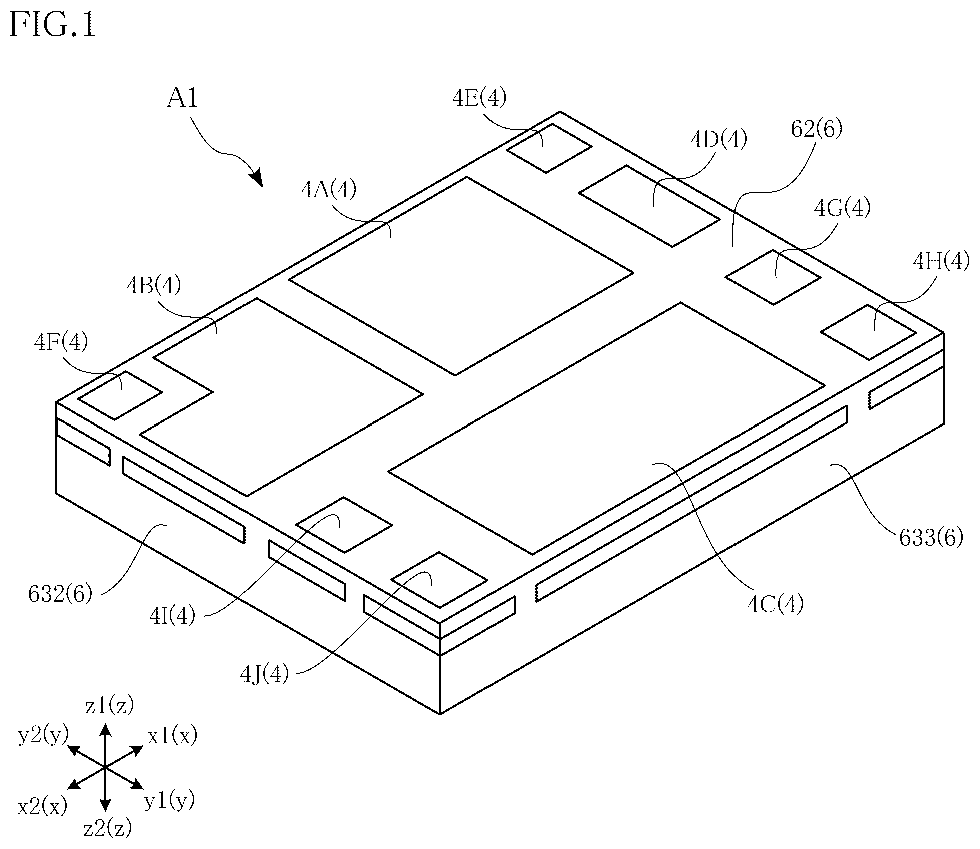
First, a module structure of the semiconductor device A 1 according to the first embodiment will be described with reference to to 6 . The module structure of the semiconductor device A 1 includes two semiconductor elements 1 and 2 , a control element 3 , a lead frame 4 , a plurality of connection members 5 , and a sealing member 6 . In the semiconductor device A 1 , the lead frame 4 includes a plurality of leads 4 A to 4 J that are separate from one another. The plurality of connection members 5 include a plurality of wires 5 A to 5 N.
is a perspective view showing the semiconductor device A 1 as viewed from the bottom face side. is a plan view showing the semiconductor device A 1 , and the sealing member 6 is shown with an imaginary line (two-dot dash line). is a bottom view showing the semiconductor device A 1 , and the sealing member 6 is shown with an imaginary line (two-dot dash line). is a cross-sectional view taken along line IV-IV in . is a cross-sectional view taken along line V-V in . is a cross-sectional view taken along line VI-VI in . It should be noted that, in to 6 , the plurality of connection members 5 are not shown.
For illustrative reasons, three directions that are perpendicular to one another are defined as an x direction, a y direction, and a z direction. The z direction is a thickness direction of the semiconductor device A 1 . The x direction is a left-right direction in the plan view of the semiconductor device A 1 (see ). The y direction is a vertical direction in the plan view of the semiconductor device A 1 (see ). One side in the x direction is taken as an x 1 side, and the other side in the x direction is taken as an x 2 side. Similarly, one side in the y direction is taken as a y 1 side and the other side in the y direction is taken as a y 2 side, and one side in the z direction is taken as a z 1 side and the other side in the z direction is taken as a z 2 side. In the present disclosure, the z 1 side may also be referred to as the “lower side”, and the z 2 side may also be referred to as the “upper side”. The x direction and the y direction correspond to the “first direction” and the “second direction” recited in the claims, respectively.
The semiconductor device A 1 is to be installed on a circuit board of an electronic device or the like. The semiconductor device A 1 is a surface mount package structure, for example. In this embodiment, the semiconductor device A 1 is of a package type called “SON (Small Outline Non-Lead)”, for example.
Both of the two semiconductor elements 1 and 2 are elements that exert an electrical function of the semiconductor device A 1 . The semiconductor elements 1 and 2 are switching elements, and are n-type MOSFETs, for example. It should be noted that the semiconductor elements 1 and 2 are not limited to n-type MOSFETs, and may also be p-type MOSFETs. In addition, the semiconductor elements 1 and 2 are not limited to MOSFETs, and may also be field effect transistors such as MISFETs (Metal-Insulator-Semiconductor FETs) and HEMTs (High Electron Mobility Transistors), bipolar transistors, or other transistors such as IGBTs (Insulated Gate Bipolar Transistors).
As shown in , the semiconductor elements 1 and 2 have a rectangular shape, for example, in a plan view (as viewed in the z direction). The semiconductor element 1 is mounted on the lead 4 A, and the semiconductor element 2 is mounted on the lead 4 B. As shown in , the two semiconductor elements 1 and 2 are disposed side by side in the x direction. In the illustrated example, the two elements 1 and 2 are aligned with each other along the x direction with a predetermined space present between them in plan view. The constituent materials of the semiconductor elements 1 and 2 include GaN (gallium nitride), for example. It should be noted that the constituent materials of the semiconductor elements 1 and 2 are not limited to GaN, and may also include SiC (silicon carbide), Si (silicon), GaAs (gallium arsenide), or Ga 2 O 3 (gallium oxide), for example. The semiconductor element 1 corresponds to the “first semiconductor element” recited in the claims, and the semiconductor element 2 corresponds to the “second semiconductor element” recited in the claims.
The semiconductor element 1 includes an element obverse surface 1 a and an element reverse surface 1 b . The element obverse surface 1 a and the element reverse surface 1 b are spaced apart from each other in the z direction. The element obverse surface 1 a faces the z 2 side, and the element reverse surface 1 b faces the z 1 side. The element reverse surface 1 b is opposed to the lead 4 A. The element obverse surface 1 a corresponds to the “first obverse surface” recited in the claims, and the element reverse surface 1 b corresponds to the “first reverse surface” recited in the claims.
The semiconductor element 1 is a three-terminal element that includes three electrodes. In this embodiment, the semiconductor element 1 includes a drain electrode 11 , a source electrode 12 , and a gate electrode 13 . The drain electrode 11 , the source electrode 12 , and the gate electrode 13 are arranged on the element obverse surface 1 a . The drain electrode 11 corresponds to the “first drain electrode” recited in the claims, the source electrode 12 corresponds to the “first source electrode” recited in the claims, and the gate electrode 13 corresponds to the “first gate electrode” recited in the claims.
The drain electrode 11 includes a plurality of pad portions 111 . The pad portions 111 have a band shape extending in the x direction. The pad portions 111 are electrically connected to a drain region inside the semiconductor element 1 . The source electrode 12 includes a plurality of pad portions 121 . The pad portions 121 have a band shape extending in the x direction. The pad portions 121 are electrically connected to a source region inside the semiconductor element 1 . The pad portions 111 and the pad portions 121 are disposed side by side in the y direction in an alternately arranged manner. The gate electrode 13 includes two pad portions 131 and 132 . The pad portions 131 and 132 are electrically connected to a gate region (channel region) inside the semiconductor element 1 . The pad portions 131 and 132 are arranged on the edge portion that is located on the side farther away from the semiconductor element 2 in the x direction. The two pad portions 131 and 132 are spaced apart from each other in the y direction. In the example shown in , the pad portion 131 is arranged at the corner portion on the x 1 side and the y 1 side in a plan view. The pad portion 132 is arranged at the corner portion on the x 1 side and the y 2 side in a plan view. The two pad portions 131 and 132 have the same electrical potential. It should be noted that the gate electrode 13 does not need to include the pad portion 132 . The pad portions 131 and 132 correspond to the “first pad portions” recited in the claims.
A driving signal is input to the semiconductor element 1 from the control element 3 , and the electrical communication state and the blocked state are switched in accordance with the driving signal (switching operation is performed). The driving signal is input to the gate electrode 13 . The semiconductor element 1 corresponds to the “first semiconductor element” recited in the claims.
The semiconductor element 2 includes an element obverse surface 2 a and an element reverse surface 2 b . The element obverse surface 2 a and the element reverse surface 2 b are spaced apart from each other in the z direction. The element obverse surface 2 a faces the z 2 side, and the element reverse surface 2 b faces the z 1 side. The element reverse surface 2 b is opposed to the lead 4 B. The element obverse surface 2 a corresponds to the “second obverse surface” recited in the claims, and the element reverse surface 2 b corresponds to the “second reverse surface” recited in the claims.
The semiconductor element 2 is a three-terminal element that includes three electrodes. In this embodiment, the semiconductor element 2 includes a drain electrode 21 , a source electrode 22 , and a gate electrode 23 . The drain electrode 21 , the source electrode 22 , and the gate electrode 23 are arranged on the element obverse surface 2 a . The drain electrode 21 corresponds to the “second drain electrode” recited in the claims, the source electrode 22 corresponds to the “second source electrode” recited in the claims, and the gate electrode 23 corresponds to the “second gate electrode” recited in the claims.
The drain electrode 21 includes a plurality of pad portions 211 . The pad portions 211 have a band shape extending in the x direction. The pad portions 211 are electrically connected to a drain region inside the semiconductor element 2 . The source electrode 22 includes a plurality of pad portions 221 . The pad portions 221 have a band shape extending in the x direction. The pad portions 221 are electrically connected to a source region inside the semiconductor element 2 . The pad portions 211 and the pad portions 221 are disposed side by side in the y direction in an alternately arranged manner. The gate electrode 23 includes two pad portions 231 and 232 . The pad portions 231 and 232 are electrically connected to a gate region (channel region) inside the semiconductor element 2 . The pad portions 231 and 232 are arranged on the edge portion that is located on the side farther away from the semiconductor element 1 in the x direction. The two pad portions 231 and 232 are spaced apart from each other in the y direction. In the example shown in , the pad portion 231 is arranged at the corner portion on the x 2 side and the y 1 side in a plan view. The pad portion 232 is arranged at the corner portion on the x 2 side and the y 2 side in a plan view. The two pad portions 231 and 232 have the same electrical potential. It should be noted that the gate electrode 23 does not need to include the pad portion 232 . The pad portions 231 and 232 correspond to the “second pad portions” recited in the claims.
A driving signal is input to the semiconductor element 2 from the control element 3 , and the electrical communication state and the blocked state are switched in accordance with the driving signal (switching operation is performed). The driving signal is input to the gate electrode 23 . The semiconductor element 2 corresponds to the “second semiconductor element” recited in the claims.
The control element 3 controls the switching operations performed by the two semiconductor elements 1 and 2 . The control element 3 generates the driving signals for driving the semiconductor elements 1 and 2 , and outputs the generated driving signals to the semiconductor elements 1 and 2 . The control element 3 is an IC (Integrated Circuit), for example. The control element 3 is a semiconductor element made of a material including a semiconductor material. The control element 3 is mounted on the lead 4 C. The control element 3 overlaps with portions of the semiconductor elements 1 and 2 as viewed in the y direction.
The control element 3 includes an element obverse surface 3 a and an element reverse surface 3 b . The element obverse surface 3 a and the element reverse surface 3 b are spaced apart from each other in the z direction. The element obverse surface 3 a faces the z 2 side, and the element reverse surface 3 b faces the z 1 side. The element reverse surface 3 b is opposed to the lead 4 C.
The control element 3 includes an element electrode 31 . The element electrode 31 is arranged on the element obverse surface 3 a . The element electrode 31 includes a plurality of pad portions 311 to 318 . Each of the plurality of pad portions 311 to 318 serves as an input end or output end in the control element 3 . The pad portions 311 to 318 are portions to which the connection members 5 are joined. The arrangement of the pad portions 311 to 318 in a plan view is not limited to that in the example shown in .
One end of a wire 5 L is joined to the pad portion 311 , and the pad portion 311 is electrically connected to the lead 4 H via the wire 5 L. One end of a wire 5 J is joined to the pad portion 312 , and the pad portion 312 is electrically connected to the lead 4 C via the wire 5 J. One end of a wire 5 M is joined to the pad portion 313 , and the pad portion 313 is electrically connected to the lead 4 I via the wire 5 M. One end of a wire 5 N is joined to the pad portion 314 , and the pad portion 314 is electrically connected to the lead 4 J via the wire 5 N. One end of a wire 5 F is joined to the pad portion 315 , and the pad portion 315 is electrically connected to the gate electrode 13 (pad portion 131 ) of the semiconductor element 1 via the wire 5 F. One end of a wire 5 H is joined to the pad portion 316 , and the pad portion 316 is electrically connected to the gate electrode 23 (pad portion 231 ) of the semiconductor element 2 via the wire 5 H. One end of a wire 5 K is joined to the pad portion 317 , and the pad portion 317 is electrically connected to the lead 4 G via the wire 5 K. One end of a wire 5 E is joined to the pad portion 318 , and the pad portion 318 is electrically connected to the lead 4 A via the wire 5 E.
The two semiconductor elements 1 and 2 and the control element 3 are mounted on the lead frame 4 . The lead frame 4 forms an electrical communication path together with the plurality of connection members 5 in the semiconductor device A 1 . The lead frame 4 is made of a conductive material. The constituent material of the lead frame 4 is a metal including Cu (copper), for example. It should be noted that the constituent material may also be a metal other than Cu. The surface of the lead frame 4 may be plated as appropriate. As shown in , the lead frame 4 includes the plurality of leads 4 A to 4 J that are spaced apart from one another. Portions of the leads 4 A to 4 J are exposed from the sealing member 6 . These exposed portions serve as terminals at the time of installing the semiconductor device A 1 on an external circuit board.
The semiconductor element 1 is mounted on the lead 4 A. One end of each of the plurality of wires 5 B is joined to the lead 4 A, and the lead 4 A is electrically connected to the source electrode 12 of the semiconductor element 1 via the wires 5 B. One end of each of the plurality of wires 5 C is joined to the lead 4 A, and the lead 4 A is electrically connected to the drain electrode 21 of the semiconductor element 2 via the wires 5 C. Furthermore, one end of the wire 5 E is joined to the lead 4 A, and the lead 4 A is electrically connected to the element electrode 31 (pad portion 318 ) of the control element 3 via the wire 5 E. The semiconductor element 2 is mounted on the lead 4 B. One end of each of the plurality of wires 5 D is joined to the lead 4 B, and the lead 4 B is electrically connected to the source electrode 22 of the semiconductor element 2 via the wires 5 D. The control element 3 is mounted on the lead 4 C. One end of the wire 5 J is joined to the lead 4 C, and the lead 4 C is electrically connected to the element electrode 31 (pad portion 312 ) of the control element 3 via the wire 5 J. One end of each of the plurality of wires 5 A is joined to the lead 4 D, and the lead 4 D is electrically connected to the drain electrode 11 of the semiconductor element 1 via the wires 5 A. One end of the wire 5 G is joined to the lead 4 E, and the lead 4 E is electrically connected to the gate electrode 13 (pad portion 132 ) of the semiconductor element 1 via the wire 5 G. One end of the wire 5 I is joined to the lead 4 F, and the lead 4 F is electrically connected to the gate electrode 23 (pad portion 232 ) of the semiconductor element 2 via the wire 5 I. One end of the wire 5 K is joined to the lead 4 G, and the lead 4 G is electrically connected to the element electrode 31 (pad portion 317 ) of the control element 3 via the wire 5 K. One end of the wire 5 L is joined to the lead 4 H, and the lead 4 H is electrically connected to the element electrode 31 (pad portion 311 ) of the control element 3 via the wire 5 L. One end of the wire 5 M is joined to the lead 4 I, and the lead 4 I is electrically connected to the element electrode 31 (pad portion 313 ) of the control element 3 via the wire 5 M. One end of the wire 5 N is joined to the lead 4 J, and the lead 4 J is electrically connected to the element electrode 31 (pad portion 314 ) of the control element 3 via the wire 5 N.
As shown in , the lead 4 A includes a die pad portion 411 and a bonding portion 412 . The die pad portion 411 and the bonding portion 412 are formed in one piece, in other words, formed integral with each other. It should be noted that the die pad portion 411 and the bonding portion 412 may also be separate from each other.
The die pad portion 411 is a portion on which the semiconductor element 1 is mounted. The semiconductor element 1 is joined to the die pad portion 411 via a joining material (not shown). The die pad portion 411 is opposed to the element reverse surface 1 b . The die pad portion 411 corresponds to the “first die pad portion” recited in the claims.
The bonding portion 412 is a portion to which some of the plurality of connection members 5 are joined. In this embodiment, one end of each of the plurality of wires 5 B, the plurality of wires 5 C and the wire 5 E is joined to the bonding portion 412 . The bonding portion 412 is electrically connected to the source electrode 12 of the semiconductor element 1 via the plurality of wires 5 B, and is electrically connected to the drain electrode 21 of the semiconductor element 2 via the plurality of wires 5 C. In addition, the bonding portion 412 is electrically connected to the element electrode 31 (pad portion 318 ) of the control element 3 via the wire 5 E. The bonding portion 412 is arranged between the semiconductor element 1 and the semiconductor element 2 in a plan view. The bonding portion 412 corresponds to the “first bonding portion” recited in the claims.
As shown in , the lead 4 B includes a die pad portion 421 and a bonding portion 422 . The die pad portion 421 and the bonding portion 422 are formed in one piece. It should be noted that the die pad portion 421 and the bonding portion 422 may also be separate from each other.
The die pad portion 421 is a portion on which the semiconductor element 2 is mounted. The semiconductor element 2 is joined to the die pad portion 421 via a joining material (not shown). The die pad portion 421 is opposed to the element reverse surface 2 b . The die pad portion 421 corresponds to the “second die pad portion” recited in the claims.
The bonding portion 422 is a portion to which some of the plurality of connection members 5 are joined. In this embodiment, one end of each of the plurality of wires 5 D is joined to the bonding portion 422 . The bonding portion 422 is electrically connected to the source electrode 22 of the semiconductor element 2 via the plurality of wires 5 D. The bonding portion 422 corresponds to the “second bonding portion” recited in the claims.
As shown in , both the lead 4 A and the lead 4 B are arranged on the y 2 side with respect to the lead 4 C. Both the lead 4 A and the lead 4 B overlap with the lead 4 C as viewed in the y direction, and do not overlap with the lead 4 C as viewed in the x direction. The lead 4 A and the lead 4 B are adjacent to each other in the x direction. The lead 4 A and the lead 4 B overlap with each other as viewed in the x direction.
The lead 4 E and the lead 4 F overlap with each other as viewed in the x direction. As shown in , the lead 4 E is arranged near the pad portion 132 in a plan view, and is closer to the pad portion 132 than the other leads (excluding the lead 4 A) are. As shown in , the lead 4 F is arranged near the pad portion 232 in a plan view, and is closer to the pad portion 232 than the other leads (excluding the lead 4 B) are.
The lead 4 D and the bonding portion 422 of the lead 4 B overlap with each other as viewed in the x direction. The lead 4 D, the lead 4 A, and the lead 4 B overlap with one another as viewed in the x direction, and are disposed side by side in the x direction. The lead 4 D is electrically connected to the drain electrode 11 of the semiconductor element 1 , the lead 4 A is electrically connected to the source electrode 12 of the semiconductor element 1 and the drain electrode 21 of the semiconductor element 2 , and the lead 4 B is electrically connected to the source electrode 22 of the semiconductor element 2 . Accordingly, the electrical current path from the lead 4 D to the lead 4 B via the two semiconductor elements 1 and 2 is formed extending in the x direction.
The lead 4 E, the lead 4 D, the lead 4 G, and the lead 4 H overlap with one another as viewed in the y direction, and are disposed side by side in the y direction. The lead 4 F, the bonding portion 422 of the lead 4 B, the lead 4 I, and the lead 4 J overlap with one another as viewed in the y direction, and are disposed side by side in the y direction.
The lead 4 G, the lead 4 H, the lead 4 I, and the lead 4 J overlap with the lead 4 C as viewed in the x direction. The two leads 4 G and 4 H are arranged on the x 1 side with respect to the lead 4 C, and the two leads 4 I and 4 J are arranged on the x 2 side with respect to the lead 4 C. The lead 4 G and the lead 4 I overlap with each other as viewed in the x direction. The lead 4 H and the lead 4 J overlap with each other as viewed in the x direction.
As shown in to 6 , each of the leads 4 A to 4 J is provided with a recessed portion 49 . In each of the leads 4 A to 4 J, the recessed portion 49 is a portion that is recessed toward the z 2 side from the surface facing the z 1 side. As shown in , in each of the leads 4 A to 4 J, the recessed portion 49 is formed along the outer peripheral edge in a plan view. The recessed portions 49 are covered by the sealing member 6 . In the example shown in to 6 , the wall surfaces of the recessed portions 49 are curved, but do not need to be curved. The recessed portions 49 are formed to prevent dislodgement of the leads 4 A to 4 J.
In this embodiment, the lead 4 A corresponds to the “first lead” recited in the claims. The lead 4 B corresponds to the “second lead” recited in the claims. The lead 4 C corresponds to the “third lead” recited in the claims. The lead 4 D corresponds to the “fourth lead” recited in the claims. The lead 4 E corresponds to the “fifth lead” recited in the claims. The lead 4 F corresponds to the “sixth lead” recited in the claims. The leads 4 G to 4 J correspond to the “seventh leads” recited in the claims.
Each of the plurality of connection members 5 enables electrical communication between two members that are spaced apart. Each of the connection members 5 is made of a conductive material. As shown in , the plurality of connection members 5 include the plurality of wires 5 A to 5 N. The wires 5 A to 5 N are so-called bonding wires. The constituent material of the wires 5 A to 5 N may be any of a metal including Au (gold), a metal including Al (aluminum), and a metal including Cu, for example.
As shown in , one end of each of the plurality of wires 5 A is joined to the pad portion 111 of the drain electrode 11 of the semiconductor element 1 , and the other end thereof is joined to the lead 4 D. One end of each of the plurality of wires 5 B is joined to the pad portion 121 of the source electrode 12 of the semiconductor element 1 , and the other end thereof is joined to the bonding portion 412 of the lead 4 A. One end of each of the plurality of wires 5 C is joined to the pad portion 211 of the drain electrode 21 of the semiconductor element 2 , and the other end thereof is joined to the bonding portion 412 of the lead 4 A. One end of each of the plurality of wires 5 D is joined to the pad portion 221 of the source electrode 22 of the semiconductor element 2 , and the other end thereof is joined to the bonding portion 422 of the lead 4 B. One end of the wire 5 E is joined to the pad portion 318 of the element electrode 31 of the control element 3 , and the other end thereof is joined to the bonding portion 412 of the lead 4 A. One end of the wire 5 F is joined to the pad portion 315 of the element electrode 31 of the control element 3 , and the other end thereof is joined to the pad portion 131 of the gate electrode 13 of the semiconductor element 1 . One end of the wire 5 G is joined to the lead 4 E, and the other end thereof is joined to the pad portion 132 of the gate electrode 13 of the semiconductor element 1 . One end of the wire 5 H is joined to the pad portion 316 of the element electrode 31 of the control element 3 , and the other end thereof is joined to the pad portion 231 of the gate electrode 23 of the semiconductor element 2 . One end of the wire 5 I is joined to the lead 4 F, and the other end thereof is joined to the pad portion 232 of the gate electrode 23 of the semiconductor element 2 . One end of the wire 5 J is joined to the pad portion 312 of the element electrode 31 of the control element 3 , and the other end thereof is joined to the lead 4 C. One end of the wire 5 K is joined to the pad portion 317 of the element electrode 31 of the control element 3 , and the other end thereof is joined to the lead 4 G. One end of the wire 5 L is joined to the pad portion 311 of the element electrode 31 of the control element 3 , and the other end thereof is joined to the lead 4 H. One end of the wire 5 M is joined to the pad portion 313 of the element electrode 31 of the control element 3 , and the other end thereof is joined to the lead 4 I. One end of the wire 5 N is joined to the pad portion 314 of the element electrode 31 of the control element 3 , and the other end thereof is joined to the lead 4 J.
In the example shown in , three wires 5 A are joined to each of the three pad portions 111 . Three wires 5 B are joined to each of the two pad portions 121 . Similarly, three wires 5 C are joined to each of the three pad portions 211 . Three wires 5 D are joined to each of the two pad portions 221 . Furthermore, the portion of the wire 5 E that is joined to the bonding portion 412 is located between the portions of the wires 5 B that are joined to the bonding portions 412 and the portions of the wires 5 C that are joined to the bonding portion 412 , in the x direction. It should be noted that the numbers of the wires 5 A to 5 N are not limited to the numbers shown in , and may be changed as appropriate in consideration of the areas of the pad portions 111 , 121 , 131 , 132 , 211 , 221 , 231 , 232 , and 311 to 318 in a plan view, the diameters of the wires 5 A to 5 N, the amounts of electrical current flowing through the wires 5 A to 5 N, and the like.
In this embodiment, the wires 5 A correspond to the “first connection member” recited in the claims. The wires 5 B correspond to the “second connection member” recited in the claims. The wires 5 C correspond to the “third connection member” recited in the claims. The wires 5 D correspond to the “fourth connection member” recited in the claims. The wire 5 E corresponds to the “fifth connection member” recited in the claims. The wire 5 F corresponds to the “sixth connection member” recited in the claims. The wire 5 G corresponds to the “seventh connection member” recited in the claims. The wire 5 H corresponds to the “eighth connection member” recited in the claims. The wire 5 I corresponds to the “ninth connection member” recited in the claims. The wires 5 K to 5 N correspond to the “tenth connection members” recited in the claims.
The sealing member 6 is a member for protecting the semiconductor elements 1 and 2 and the control element 3 . The sealing member 6 covers the semiconductor elements 1 and 2 , the control element 3 , a portion of the lead frame 4 , and the plurality of connection members 5 . The constituent material of the sealing member 6 is an electrical insulating resin material such as an epoxy resin. The sealing member 6 has a rectangular shape in a plan view, for example. It should be noted that the shape of the sealing member 6 is not limited to that of the example shown in to 6 . The sealing member 6 includes a resin obverse surface 61 , a resin reverse surface 62 , and a plurality of resin side surfaces 631 to 634 .
As shown in to 6 , the resin obverse surface 61 and the resin reverse surface 62 are spaced apart in the z direction. The resin obverse surface 61 faces the z 2 side, and the resin reverse surface 62 faces the z 1 side. Portions of the leads 4 A to 4 J (surfaces facing the z 1 side) are exposed from the resin reverse surface 62 . The plurality of resin side surfaces 631 to 634 are sandwiched between the resin obverse surface 61 and the resin reverse surface 62 in the z direction and are connected to both of them. The resin side surfaces 631 and 632 are spaced apart in the x direction, and the resin side surface 631 faces the x 1 side and the resin side surface 632 faces the x 2 side. The resin side surfaces 633 and 634 are spaced apart in the y direction, and the resin side surface 633 faces the y 1 side and the resin side surface 634 faces the y 2 side.
Next, the circuit configuration of the semiconductor device A 1 according to the first embodiment will be described with reference to . It should be noted that the reference electrical potential may be referred to as the “ground voltage V GND ” in the following description.
shows a circuit diagram in a case where the semiconductor device A 1 is applied to a synchronous rectification-type step-down DC/DC converter. The DC/DC converter is a power circuit that steps down an input voltage Vin and generates a desired output voltage Vout. The output voltage Vout is supplied to a load L 0 . It should be noted that the circuit diagram shown in is merely an example.
As shown in , the circuit configuration of the semiconductor device A 1 includes a plurality of external terminals T 1 to T 10 , two semiconductor elements 1 and 2 , and a control element 3 . In addition, as shown in , two external power sources PS 1 and PS 2 and a plurality of discrete components (a plurality of capacitors C 1 to C 4 and an inductor L 1 ) are connected to the semiconductor device A 1 . It should be noted that one or more of the plurality of discrete components may be built into the semiconductor device A 1 .
The external power source PS 1 generates a power source voltage VCC for driving the control element 3 . The high-potential side terminal of the external power source PS 1 is connected to the external terminal T 1 . The low-potential side terminal of the external power source PS 1 is connected to a first ground end GND 1 , and is grounded at a reference electrical potential. The capacitor C 1 is connected to the external power source PS 1 in parallel. The capacitor C 1 is a bypass capacitor that stabilizes the power source voltage VCC.
The external power source PS 2 generates an input voltage Vin. The high-potential side terminal of the external power source PS 2 is connected to the external terminal T 3 . The low-potential side terminal of the external power source PS 2 is connected to a second ground end GND 2 , and is grounded at a reference electrical potential. It should be noted that a case where both the first ground end GND 1 and the second ground end GND 2 are ground ends at a reference electrical potential is shown, but the reference electrical potential of the first ground end GND 1 and the reference electrical potential of the second ground end GND 2 may be different from each other. The capacitor C 2 is connected to the external power source PS 2 in parallel. The capacitor C 2 is a bypass capacitor that stabilizes the input voltage Vin.
A first end of the inductor L 1 is connected to the external terminal T 7 , and a second end thereof is connected to the load L 0 and the capacitor C 3 . A first end of the capacitor C 3 is connected to the inductor L 1 , and a second end thereof is connected to the second ground end GND 2 . The inductor L 1 and the capacitor C 3 form an LC filter circuit. A first end of the capacitor C 4 is connected to the external terminal T 7 , and a second end thereof is connected to the external terminal T 8 . The capacitor C 4 forms a bootstrap circuit together with a diode D 1 , which will be described later. The capacitor C 4 generates a boot voltage VB.
The external terminal T 1 is an input end to which the power source voltage VCC is input. The external terminal T 1 is connected to the high-potential side terminal of the external power source PS 1 . The external terminal T 1 is connected to the control element 3 (a connection terminal TC 1 , which will be described later) inside the semiconductor device A 1 . The external terminal T 1 corresponds to the lead 4 H in the module structure of the semiconductor device A 1 , for example.
The external terminal T 2 is connected to the first ground end GND 1 , and is grounded at a reference electrical potential. The external terminal T 2 is connected to the control element 3 (a connection terminal TC 2 , which will be described later) inside the semiconductor device A 1 . The external terminal T 2 corresponds to the lead 4 C in the module structure of the semiconductor device A 1 , for example.
The external terminal T 3 is an input end to which the input voltage Vin is input. The external terminal T 3 is connected to the high-potential side terminal of the external power source PS 2 . The external terminal T 3 is connected to a drain of the semiconductor element 1 inside the semiconductor device A 1 . The external terminal T 3 corresponds to the lead 4 D in the module structure of the semiconductor device A 1 , for example.
The external terminal T 4 is connected to the second ground end GND 2 , and is grounded at a reference electrical potential. The external terminal T 4 is connected to a source of the semiconductor element 2 inside the semiconductor device A 1 . The external terminal T 4 corresponds to the lead 4 B in the module structure of the semiconductor device A 1 , for example.
The external terminal T 5 is an input end to which a control signal SH is input. The control signal SH is a signal for controlling the switching operations performed by the semiconductor element 1 . The control signal SH is a rectangular pulse wave in which a high level and a low level are alternately switched, for example. The external terminal T 5 is connected to the control element 3 (a connection terminal TC 3 , which will be described later) inside the semiconductor device A 1 . The external terminal T 5 corresponds to the lead 4 I in the module structure of the semiconductor device A 1 , for example.
The external terminal T 6 is an input end to which a control signal SL is input. The control signal SL is a signal for controlling the switching operation performed by the semiconductor element 2 . The control signal SL is a rectangular pulse wave in which a high level and a low level are alternately switched, for example. The high-level period and the low-level period are inverted between the control signal SL and the control signal SH. The external terminal T 6 is connected to the control element 3 (a connection terminal TC 4 , which will be described later) inside the semiconductor device A 1 . The external terminal T 6 corresponds to the lead 4 J in the module structure of the semiconductor device A 1 , for example.
The external terminal T 7 is an output end from which an output voltage V SW is output. The output voltage V SW is a voltage signal generated through the switching operations performed by the semiconductor element 1 and the semiconductor element 2 . The external terminal T 7 is connected to the connection point where the source of the semiconductor element 1 and the drain of the semiconductor element 2 are connected to each other inside the semiconductor device A 1 . The external terminal T 7 corresponds to the lead 4 A in the module structure of the semiconductor device A 1 , for example.
The external terminal T 8 is an input end to which the boot voltage VB is input. The boot voltage VB is a voltage signal generated by the capacitor C 4 and a diode D 1 , which will be described later. The second end of the capacitor C 4 is connected to the external terminal T 8 . The external terminal T 8 is connected to the control element 3 (a connection terminal TC 7 , which will be described later) inside the semiconductor device A 1 . The external terminal T 8 corresponds to the lead 4 G in the module structure of the semiconductor device A 1 , for example.
The external terminal T 9 is an input end to which a driving signal GH 2 is input. The driving signal GH 2 is a signal for driving the semiconductor element 1 , and is input directly from an external device (not shown). The driving signal GH 2 is a rectangular pulse wave in which a high level and a low level are alternately switched, for example. The external terminal T 9 is connected to the gate of the semiconductor element 1 inside the semiconductor device A 1 . The external terminal T 9 corresponds to the lead 4 E in the module structure of the semiconductor device A 1 , for example.
The external terminal T 10 is an input end to which a driving signal GL 2 is input. The driving signal GL 2 is a signal for driving the semiconductor element 2 , and is input directly from an external device (not shown). The driving signal GL 2 is a rectangular pulse wave in which a high level and a low level are alternately switched, for example. The high-level period and the low-level period are inverted between the driving signal GH 2 and the driving signal GL 2 . The external terminal T 10 is connected to the gate of the semiconductor element 2 inside the semiconductor device A 1 . The external terminal T 10 corresponds to the lead 4 F in the module structure of the semiconductor device A 1 , for example.
It should be noted that the correspondence relationships between the external terminals T 1 to T 10 in the circuit configuration and the leads 4 A to 4 J in the module structure are not limited to those as described above. For example, the combinations in the correspondence relationships between the external terminals T 1 , T 5 , T 6 , and T 8 and the leads 4 G to 4 J can be changed as appropriate. It is sufficient that the combinations in the correspondence relationships are changed as appropriate in accordance with the arrangement of the pad portions 311 , 313 , 314 , and 317 of the control element 3 in a plan view.
The two semiconductor elements 1 and 2 are formed of an n-type MOSFET as described above. In the semiconductor elements 1 and 2 , the electrical communication state (on state) and the blocked state (off state) are switched in accordance with driving signals GH 1 , GH 2 , GL 1 , and GL 2 input to the gates. The two semiconductor elements 1 and 2 form a half-bridge switching circuit, and the semiconductor element 1 is an upper arm of the switching circuit and the semiconductor element 2 is a lower arm of the switching circuit.
The drain of the semiconductor element 1 is connected to the external terminal T 3 , and the source of the semiconductor element 1 is connected to the drain of the semiconductor element 2 . The gate of the semiconductor element 1 is connected to the control element 3 (a connection terminal TC 5 , which will be described later) and the external terminal T 9 .
When a driving signal GH 1 is input to the gate from the control element 3 , the semiconductor element 1 performs a switching operation in accordance with the driving signal GH 1 . When a high-level driving signal GH 1 is input to the gate, the semiconductor element 1 enters the electrical communication state, and when a low-level driving signal GH 1 is input to the gate, the semiconductor element 1 enters the blocked state. In addition, when a driving signal GH 2 is input to the gate from the external terminal T 9 , the semiconductor element 1 performs a switching operation in accordance with the driving signal GH 2 . When a high-level driving signal GH 2 is input to the gate, the semiconductor element 1 enters the electrical communication state, and when a low-level driving signal GH 2 is input to the gate, the semiconductor element 1 enters the blocked state. It should be noted that the semiconductor element 1 is of a normally off type, but may also be of a normally on type. Moreover, one or both of the two driving signals GH 1 and GH 2 may be input to the gate of the semiconductor element 1 .
The drain of the semiconductor element 2 is connected to the source of the semiconductor element 1 , and the source of the semiconductor element 2 is connected to the external terminal T 4 . The gate of the semiconductor element 2 is connected to the control element 3 (a connection terminal TC 6 , which will be described later) and the external terminal T 10 .
When a driving signal GL 1 is input to the gate from the control element 3 , the semiconductor element 2 performs a switching operation in accordance with the driving signal GL 1 . When a high-level driving signal GL 1 is input to the gate, the semiconductor element 2 enters the electrical communication state, and when a low-level driving signal GL 1 is input to the gate, the semiconductor element 2 enters the blocked state. In addition, when a driving signal GL 2 is input to the gate from the external terminal T 10 , the semiconductor element 2 performs a switching operation in accordance with the driving signal GL 2 . When a high-level driving signal GL 2 is input to the gate, the semiconductor element 2 enters the electrical communication state, and when a low-level driving signal GL 2 is input to the gate, the semiconductor element 2 enters the blocked state. It should be noted that the semiconductor element 2 is of a normally off type, but may also be of a normally on type. Moreover, one or both of the two driving signals GL 1 and GL 2 may be input to the gate of the semiconductor element 2 .
The connection point where the source of the semiconductor element 1 and the drain of the semiconductor element 2 are connected to each other is connected to the external terminal T 7 and the control element 3 (a connection terminal TC 8 , which will be described later). The output voltage V SW is applied to the external terminal T 7 due to the switching operation performed by the semiconductor element 1 and the switching operation performed by the semiconductor element 2 .
The control element 3 mainly controls the switching operations performed by the two semiconductor elements 1 and 2 . The control element 3 generates the driving signals GH 1 and GL 1 based on the control signals SH and SL, and inputs the generated driving signals GH 1 and GL 1 to the semiconductor elements 1 and 2 . The internal circuit of the control element 3 includes a plurality of connection terminals TC 1 to TC 8 , two driving circuits DR 1 and DR 2 , and a diode D 1 . The control element 3 is an IC obtained by integrating the two driving circuits DR 1 and DR 2 and the diode D 1 in one chip.
The connection terminal TC 1 is connected to the external terminal T 1 , and serves as an input end to which the power source voltage VCC is input in the control element 3 . The connection terminal TC 2 is connected to the external terminal T 2 , and is ground at a reference electrical potential. The connection terminal TC 3 is connected to the external terminal T 5 , and serves as an input end to which the control signal SH is input in the control element 3 . The connection terminal TC 4 is connected to the external terminal T 6 , and serves as an input end to which the control signal SL is input in the control element 3 . The connection terminal TC 5 serves as an output end from which the driving signal GH 1 is output. The connection terminal TC 5 is connected to the gate of the semiconductor element 1 . The connection terminal TC 6 serves as an output end from which the driving signal GL 1 is output. The connection terminal TC 6 is connected to the gate of the semiconductor element 2 . The connection terminal TC 7 is connected to the external terminal T 8 , and serves as an input end to which the boot voltage VB is input in the control element 3 . The connection terminal TC 8 is connected to the connection point where the semiconductor element 1 (source) and the semiconductor element 2 (drain) are connected to each other.
The driving circuit DR 1 generates the driving signal GH 1 based on the input control signal SH. The driving signal GH 1 is a signal for allowing the semiconductor element 1 to perform a switching operation, and is obtained by increasing the strength of the control signal SH to a level necessary for the semiconductor element 1 to perform the switching operation. The driving circuit DR 1 outputs the generated driving signal GH 1 from the connection terminal TC 5 . Since the connection terminal TC 5 is connected to the gate of the semiconductor element 1 , the driving signal GH 1 is input to the gate of the semiconductor element 1 . The driving signal GH 1 is a signal for setting the boot voltage VB to a high level and the source voltage of the semiconductor element 1 to a low level. The source voltage of the semiconductor element 1 is input to the driving circuit DR 1 via the connection terminal TC 8 . The gate voltage of the semiconductor element 1 is applied on the basis of the source voltage of the semiconductor element 1 .
The driving circuit DR 2 generates the driving signal GL 1 based on the input control signal SL. The driving signal GL 1 is a signal for making the semiconductor element 2 perform a switching operation, and is obtained by increasing the strength of the control signal SL to a level necessary for the semiconductor element 2 to perform the switching operation. The driving circuit DR 2 outputs the generated driving signal GL 1 from the connection terminal TC 6 . Since the connection terminal TC 6 is connected to the gate of the semiconductor element 2 , the driving signal GL 1 is input to the gate of the semiconductor element 2 . The driving signal GL 1 is a signal for setting the power source voltage VCC to a high level and the ground voltage V GND to a low level. The gate voltage of the semiconductor element 2 is applied on the basis of the ground voltage V GND .
An anode of the diode D 1 is connected to the connection terminal TC 1 , and the cathode thereof is connected to the connection terminal TC 7 . The diode D 1 forms a bootstrap circuit together with the capacitor C 4 . The bootstrap circuit generates the boot voltage VB and supplies this boot voltage VB to the driving circuit DR 1 . It should be noted that the diode D 1 may be arranged outside the control element 3 .
Next, an operational example of the semiconductor device A 1 will be described.
In the semiconductor device A 1 , the control element 3 generates the driving signals GH 1 and GL 1 when the control signals SH and SL are input to the control element 3 from the external terminals T 5 and T 6 . Then, the driving signals GH 1 and GL 1 are respectively input to the gates of the semiconductor elements 1 and 2 from the control element 3 . Alternatively, the driving signals GH 2 and GL 2 are respectively input to the gates of the semiconductor elements 1 and 2 from the external terminals T 9 and T 10 . Thus, a first period in which the semiconductor element 1 is in the electrical communication state and the semiconductor element 2 is in the blocked state, and a second period in which the semiconductor element 1 is in the blocked state and the semiconductor element 2 is in the electrical communication state are alternately repeated. At this time, the input voltage Vin is applied to the external terminal T 7 during the first period. On the other hand, the external terminal T 7 is ground at a reference electrical potential (the ground voltage V GND is applied to the external terminal T 7 ) during the second period. Accordingly, the output voltage V SW output from the external terminal T 7 is a pulse wave in which the input voltage Vin corresponds to the high-level voltage and the ground voltage V GND corresponds to the low-level voltage. The output voltage V SW is smoothed by the inductor L 1 and the capacitor 3 and thus converted to the output voltage Vout, which is a D.C. voltage. Due to the semiconductor device A 1 operating as described above, the input voltage Vin is transformed (stepped down) to the output voltage Vout.
The first period and the second period are alternately repeated in a predetermined cycle, and the step-down ratio can be changed depending on the ratio between the first period and the second period in one cycle. For example, when the first period makes up 25% of one cycle (i.e., the second period makes up 75% of one cycle), the input voltage Vin is transformed by a factor of ¼ (Vout=Vin×(25/100)) to obtain the output voltage Vout. It should be noted that a dead time in which both the semiconductor elements 1 and 2 are in the blocked state may be provided between the first period and the second period.
Functions and effects of the semiconductor device A 1 configured as described above are as follows.
With the first embodiment, the semiconductor device A 1 includes the lead 4 A, the lead 4 B, and the lead 4 C. The lead 4 A and the lead 4 B overlap with each other as viewed in the x direction, and the lead 4 C overlaps with both the lead 4 A and the lead 4 B as viewed in the y direction. The semiconductor element 1 is mounted on the lead 4 A, the semiconductor element 2 is mounted on the lead 4 B, and the control element 3 is mounted on the lead 4 C. Accordingly, the separation distance between the semiconductor element 1 and the semiconductor element 2 can be reduced compared with the semiconductor device disclosed in JP 2003-218309A. Specifically, in the semiconductor device disclosed in JP 2003-218309A, two semiconductor elements (switching elements) are arranged on sides opposite to each other with a control element (control IC) located therebetween in a plan view. Therefore, it is necessary to install wiring around the control element in order to connect the two semiconductor elements to each other, and thus the wiring distance tends to increase. On the other hand, in the semiconductor device A 1 , the control element 3 is not arranged between the semiconductor element 1 and the semiconductor element 2 , and thus the length of wiring that connects the semiconductor element 1 and the semiconductor element 2 to each other (the lengths of the wires 5 B and 5 C, and a portion of the lead 4 A in this embodiment) can be reduced. Accordingly, with the semiconductor device A 1 , a parasitic inductance and a parasitic resistance can be reduced, thus making it possible to improve the efficiency and reduce power consumption.
With the first embodiment, both the lead 4 A and the lead 4 B are arranged on the y 2 side with respect to the lead 4 C, and overlap with the lead 4 C as viewed in the y direction. Accordingly, the lead 4 A on which the semiconductor element 1 is mounted and the lead 4 B on which the semiconductor element 2 is mounted can be arranged on one side (y 2 side) in the y direction, and the lead 4 C on which the control element 3 is mounted can be arranged on the other side (y 1 side) in the y direction. When an electrical current is applied to the semiconductor device A 1 , the semiconductor elements 1 and 2 and the control element 3 generate heat. The amount of heat generated by the semiconductor elements 1 and 2 is larger than the amount of heat generated by the control element 3 . If the heat generated by the semiconductor elements 1 and 2 is transferred to the control element 3 , a malfunction and a decrease in performance may occur in the control element 3 due to the heat generated by the semiconductor elements 1 and 2 . However, with the semiconductor device A 1 , the lead 4 A and 4 B are arranged on one side (y 2 side) in the y direction with respect to the lead 4 C, and thus the semiconductor elements 1 and 2 are arranged away from the control element 3 . Accordingly, with the semiconductor device A 1 , the transfer of heat generated by the semiconductor elements 1 and 2 to the control element 3 is suppressed, thus making it possible to inhibit a malfunction and a decrease in performance from occurring in the control element 3 .
With the first embodiment, the lead 4 D, the lead 4 A, and the lead 4 B overlap with one another as viewed in the x direction, and are disposed side by side in the x direction. The pad portions 111 , 121 , 211 , and 221 of the semiconductor elements 1 and 2 have a band shape extending in the x direction. Accordingly, with the semiconductor device A 1 , the electrical current path between the drain and the source of the semiconductor element 1 and the electrical current path between the drain and the source of the semiconductor element 2 (power system electrical current paths) can be linearly routed. These power system electrical current paths are electrical current paths used in power conversion performed in the semiconductor device A 1 . Particularly in the case where the semiconductor elements 1 and 2 are driven at a high frequency, the power system electrical current paths do not need to be bent at a right angle when routed, which is an effective measure against noise.
With the first embodiment, the lead 4 A includes the die pad portion 411 and the bonding portion 412 , which are formed in one piece. This makes it possible to diffuse heat generated by the semiconductor element 1 to not only the die pad portion 411 but also the bonding portion 412 . Accordingly, with the semiconductor device A 1 , it is possible to suppress an increase in the junction temperature in the semiconductor element 1 caused by the heat generated by the semiconductor element 1 . An increase in the junction temperature causes damage to the semiconductor element 1 . In other words, with the semiconductor device A 1 , damage to the semiconductor element 1 can be suppressed. Similarly, the lead 4 B includes the die pad portion 421 and the bonding portion 422 , which are formed in one piece. This makes it possible to diffuse heat generated by the semiconductor element 2 to not only the die pad portion 421 but also the bonding portion 422 . Accordingly, with the semiconductor device A 1 , it is possible to suppress an increase in the junction temperature in the semiconductor element 2 caused by the heat generated by the semiconductor element 2 . In other words, with the semiconductor device A 1 , damage to the semiconductor element 2 can be suppressed.
With the first embodiment, the pad portion 131 of the gate electrode 13 of the semiconductor element 1 is arranged near the edge on the lead 4 C side in the y direction on the element obverse surface 1 a . This makes it possible to reduce the separation distance between the pad portion 131 and the control element 3 in the semiconductor device A 1 in a plan view. Accordingly, the length of the wire 5 F can be reduced, thus making it possible to reduce a parasitic inductance and a parasitic resistance in the wire 5 F. In particular, the wire 5 F is a wire for transmitting the driving signal GH 1 , and thus a reduction in switching operation responsiveness, and switching malfunctions can be suppressed in the semiconductor element 1 . Similarly, the pad portion 231 of the gate electrode 23 of the semiconductor element 2 is arranged near the edge on the lead 4 C side in the y direction on the element obverse surface 2 a . This makes it possible to reduce the separation distance between the pad portion 231 and the control element 3 in the semiconductor device A 1 in a plan view. Accordingly, the length of the wire 5 H can be reduced, thus making it possible to reduce a parasitic inductance and a parasitic resistance in the wire 5 H. In particular, the wire 5 H is a wire for transmitting the driving signal GL 1 , and thus a reduction in switching operation responsiveness, and switching malfunctions can be suppressed in the semiconductor element 2 .
With the first embodiment, the lead 4 E is arranged near the pad portion 132 in a plan view, and is closer to the pad portion 132 than any other leads (excluding the lead 4 A) are. Accordingly, the length of the wire 5 G that connects the lead 4 E and the pad portion 132 to each other can be reduced, thus making it possible to reduce a parasitic inductance and a parasitic resistance in the wire 5 G. In particular, the wire 5 G serves as a wire for transmitting the driving signal GH 2 when the driving signal GH 2 is input to the semiconductor device A 1 from an external device, and thus a reduction in switching operation responsiveness, and switching malfunctions can be suppressed in the semiconductor element 1 . Moreover, the lead 4 F is arranged near the pad portion 232 in a plan view, and is closer to the pad portion 232 than any other leads (excluding the lead 4 B) are. Accordingly, the length of the wire 5 I that connects the lead 4 F and the pad portion 232 to each other can be reduced, thus making it possible to reduce a parasitic inductance and a parasitic resistance in the wire 5 I. In particular, the wire 5 I serves as a wire for transmitting the driving signal GL 2 when the driving signal GL 2 is input to the semiconductor device A 1 from an external device, and thus a reduction in switching operation responsiveness, and switching malfunctions can be suppressed in the semiconductor element 2 .
Next, a semiconductor device A 2 according to a second embodiment will be described with reference to . is a plan view showing the semiconductor device A 2 , and the sealing member 6 is shown with an imaginary line (two-dot dash line).
As shown in , the semiconductor device A 2 differs from the semiconductor device A 1 in the configuration of the lead frame 4 . Specifically, the lead frame 4 of the semiconductor device A 2 does not include the leads 4 E and 4 F unlike the lead frame 4 of the semiconductor device A 1 .
As shown in , in the lead frame 4 of the semiconductor device A 2 , instead of arranging the lead 4 E, the lead 4 D is expanded to the arrangement position of the lead 4 E. Similarly, as shown in , instead of arranging the lead 4 F, the bonding portion 422 of the lead 4 B is expanded to the arrangement position of the lead 4 F. Since the leads 4 E and 4 F are not included, the plurality of connection members 5 do not include the wires 5 G and 5 I.
With the second embodiment, the semiconductor device A 2 includes the lead 4 A, the lead 4 B, and the lead 4 C as is the case with the semiconductor device A 1 . The lead 4 A and the lead 4 B overlap with each other as viewed in the x direction, and the lead 4 C overlaps with both the lead 4 A and the lead 4 B as viewed in the y direction. Accordingly, with the semiconductor device A 2 , the length of wiring that connects the semiconductor element 1 and the semiconductor element 2 to each other (the lengths of the wires 5 B and 5 C, and a portion of the lead 4 A in this embodiment) can be reduced as is the case with the semiconductor device A 1 . Accordingly, with the semiconductor device A 2 , a parasitic inductance and a parasitic resistance can be reduced, thus making it possible to improve the efficiency and reduce power consumption.
With the second embodiment, the lead 4 D of the semiconductor device A 2 is larger in size compared with the semiconductor device A 1 . Accordingly, the wiring resistance in the lead 4 D can be reduced in the semiconductor device A 2 compared with the semiconductor device A 1 . In particular, the lead 4 D is a portion of the above-described power system electrical current path, and thus power loss in power conversion can be suppressed in the semiconductor device A 2 compared with the semiconductor device A 1 . Similarly, the bonding portion 422 of the lead 4 B of the semiconductor device A 2 is larger in size compared with the semiconductor device A 1 . Accordingly, the wiring resistance in the lead 4 B can be reduced in the semiconductor device A 2 compared with the semiconductor device A 1 . In particular, the lead 4 B is a portion of the above-described power system electrical current path, and thus power loss in power conversion can be suppressed in the semiconductor device A 2 compared with the semiconductor device A 1 . Furthermore, the semiconductor element 2 is mounted on the lead 4 B, and heat generated by the semiconductor element 2 is transferred to the lead 4 B. Accordingly, the efficiency in diffusing the heat generated by the semiconductor element 2 can be improved due to the increase in the size of the lead 4 B (bonding portion 422 ).
Next, a semiconductor device A 3 according to a third embodiment will be described with reference to . is a plan view showing the semiconductor device A 3 , and the sealing member 6 is shown with an imaginary line (two-dot dash line). is a cross-sectional view taken along line X-X in . It should be noted that, also in the semiconductor device A 3 , the lead frame 4 does not need to include the leads 4 E and 4 F as is the case with the second embodiment.
As shown in , the semiconductor device A 3 differs from the semiconductor device A 1 in that the plurality of connection members 5 include clips 7 A, 7 B, 7 C, and 7 D instead of the wires 5 A, 5 B, 5 C, and 5 D. It should be noted that, in the semiconductor element 1 of the semiconductor device A 3 shown in , the plurality of pad portions 111 (drain electrode 11 ) and the plurality of pad portions 121 (source electrode 12 ) have changed places with each other compared with the semiconductor device A 1 .
The clips 7 A to 7 D are obtained by bending plate-shaped metal members. The constituent material of the clips 7 A to 7 D is a metal including Cu, a metal including A 1 , or the like, for example. Alternatively, a clad material such as CIC (Copper-Invar-Copper) may also be used. It should be noted that, in the example shown in , the clips 7 A to 7 D are bent at a right angle to the upper faces of the leads 4 A, 4 B, and 4 D, but may also be inclined to the z direction.
One side of the clip 7 A in the x direction (x 2 side in ) has a comb-like shape, and the comb-like portion is joined to the plurality of pad portions 111 . One side of the clip 7 B in the x direction (x 1 side in ) has a comb-like shape, and the comb-like portion is joined to the plurality of pad portions 121 . One side of the clip 7 C in the x direction (x 2 side in ) has a comb-like shape, and the comb-like portion is joined to the plurality of pad portions 211 . One side of the clip 7 D in the x direction (x 1 side in ) has a comb-like shape, and the comb-like portion is joined to the plurality of pad portions 221 . It should be noted that the shapes of the clips 7 A to 7 D are not limited to those of the example shown in .
With the third embodiment, the semiconductor device A 3 includes the lead 4 A, the lead 4 B, and the lead 4 C as is the case with the semiconductor device A 1 . The lead 4 A and the lead 4 B overlap with each other as viewed in the x direction, and the lead 4 C overlaps with both the lead 4 A and the lead 4 B as viewed in the y direction. Accordingly, with the semiconductor device A 3 , the length of wiring that connects the semiconductor element 1 and the semiconductor element 2 to each other (the lengths of the clips 7 B and 7 C, and a portion of the lead 4 A in this embodiment) can be reduced as is the case with the semiconductor device A 1 . Accordingly, with the semiconductor device A 3 , a parasitic inductance and a parasitic resistance can be reduced, thus making it possible to improve the efficiency and reduce power consumption.
With the third embodiment, the plurality of connection members 5 include the clip 7 A instead of the wires 5 A. The wiring resistance can be reduced in the case where the clip 7 A is used compared with the case where the wires 5 A are used. In particular, the clip 7 A is a portion of the above-described power system electrical current path, and thus power loss in power conversion can be suppressed in the semiconductor device A 3 compared with the semiconductor device A 1 . Similarly, the plurality of connection members 5 include the clips 7 B, 7 C, and 7 D instead of the wires 5 B, 5 C, and 5 D. The wiring resistance can be reduced in the case where the clips 7 B, 7 C, and 7 D are used compared with the case where the wires 5 B, 5 C, and 5 D are used. In particular, the clips 7 B, 7 C, and 7 D are portions of the above-described power system electrical current path, and thus power loss in power conversion can be suppressed in the semiconductor device A 3 compared with the semiconductor device A 1 .
In the third embodiment, each of the clips 7 A to 7 D has a structure in which a portion thereof is bent, but there is no limitation to such a structure. For example, as shown in , each of the clips 7 A to 7 D may have a structure in which the thickness (the dimension in the z direction) of a portion thereof is changed. is a cross-sectional view of a semiconductor device according to this modified example and shows a cross-section corresponding to the cross section shown in . For example, as shown in , in each of the clips 7 A to 7 D, portions joined to the semiconductor element 1 or semiconductor element 2 are thin, and portions joined to the lead 4 A, 4 B, or 4 D are thick.
In the third embodiment, the clip 7 A has a comb-like portion, and this comb-like portion is joined to the plurality of pad portions 111 (the drain electrode 11 ), but there is no limitation to this configuration. For example, a plurality of clips 7 A that each have a band shape may be provided and be respectively joined to the plurality of pad portions 111 . The same applies to the clips 7 B to 7 D.
Next, a semiconductor device A 4 according to a fourth embodiment will be described with reference to . is a plan view showing the semiconductor device A 4 , and the sealing member 6 is shown with an imaginary line (two-dot dash line). It should be noted that, also in the semiconductor device A 4 , the lead frame 4 does not need to include the leads 4 E and 4 F as is the case with the second embodiment. In addition, also in the semiconductor device A 4 , the clips 7 A to 7 D may be used instead of the wires 5 A to 5 D as is the case with the third embodiment.
As shown in , the semiconductor device A 4 differs from the semiconductor device A 1 in the configurations of the electrodes (the drain electrodes 11 and 21 , and the source electrodes 12 and 22 ) of the semiconductor elements 1 and 2 . Specifically, the shapes of the pad portions 111 , 121 , 211 , and 221 in a plan view are changed.
The pad portions 111 of the semiconductor device A 4 are tapered. Specifically, the dimensions in the y direction of the pad portions 111 decrease from the edge on the x 1 side toward the edge on the x 2 side in the x direction. The pad portions 111 have a substantially triangular shape in a plan view. Also, the pad portions 121 , the pad portions 211 , and the pad portions 221 are tapered. Specifically, the dimensions in the y direction of the pad portions 121 decrease from the edge on the x 2 side toward the edge on the x 1 side in the x direction. The dimensions in the y direction of the pad portions 211 decrease from the edge on the x 1 side toward the edge on the x 2 side in the x direction. The dimensions in the y direction of the pad portions 221 decrease from the edge on the x 2 side toward the edge on the x 1 side in the x direction. The pad portions 121 , 211 , and 221 have a substantially triangular shape in a plan view.
With the fourth embodiment, the semiconductor device A 4 includes the lead 4 A, the lead 4 B, and the lead 4 C as is the case with the semiconductor device A 1 . The lead 4 A and the lead 4 B overlap with each other as viewed in the x direction, and the lead 4 C overlaps with both the lead 4 A and the lead 4 B as viewed in the y direction. Accordingly, with the semiconductor device A 4 , the length of wiring that connects the semiconductor element 1 and the semiconductor element 2 to each other (the lengths of the wires 5 B and 5 C, and a portion of the lead 4 A in this embodiment) can be reduced as is the case with the semiconductor device A 1 . Accordingly, with the semiconductor device A 4 , a parasitic inductance and a parasitic resistance can be reduced, thus making it possible to improve the efficiency and reduce power consumption.
In the first embodiment to the fourth embodiment, each of the leads 4 A to 4 J is provided with the recessed portion 49 in the semiconductor devices A 1 to A 4 , but there is no limitation to such configurations, and the recessed portions 49 do not need to be provided. Moreover, in the semiconductor devices A 1 to A 4 , the recessed portion 49 is formed along the outer peripheral edge in each of the leads 4 A to 4 J in a plan view, but there is no limitation to such configurations. For example, as shown in , each of the leads 4 A to 4 J may be provided with a recessed portion 49 along an edge that is in contact with one of the resin side surfaces 631 to 634 in a plan view. is a perspective view showing a semiconductor device according to this modified example as viewed from the bottom face side. In this case, the sealing member 6 is provided with recessed portions 69 along the outer peripheral edge in a plan view. The recessed portions 49 and the recessed portions 69 are continuous. Solder fillets are likely to be formed when the semiconductor device shown in is installed on a circuit board of an electronic device or the like with solder. Accordingly, it is possible to increase the likelihood that the soldering state of the semiconductor device, which is a leadless package, can be visually confirmed.
In the first embodiment to the fourth embodiment, the semiconductor devices A 1 to A 4 are of the SON package type, but there is no limitation to this type, and other package types may also be employed. For example, a BGA (Ball Grid Array) package type, an LGA (Land Grid Array) package type, a QFP (Quad Flat Package) package type, a QFN (Quad Flat Non-lead) package type, and the like may also be employed. It should be noted that these package types are merely examples, and there is no limitation thereto. For example, shows a semiconductor device (bottom view) of a QFN package type.
The semiconductor device according to the present disclosure is not limited to the above-described embodiments. Various modifications in design may be made freely in the specific structure of each part of the semiconductor device according to the present disclosure.
Figures (12)
Citations
This patent cites (9)
- US11081433
- US11652033
- US11996354
- US2007/0196950
- US2013/0075880
- US2018/0040540
- US2018/0108598
- US103000592
- US2003-218309