Semiconductor Device and Method of Producing the Same, and Electronic Device
Abstract
The on-resistance of each of field effect transistors having different planar sizes is reduced. A semiconductor device includes first and second field effect transistors mounted on a semiconductor substrate and an insulating layer provided on a main surface of the semiconductor substrate. Here, each of the first and second field effect transistors includes a pair of main electrodes which are separated from each other and provided on the main surface of the semiconductor substrate, a cavity part which is provided in the insulating layer between the pair of main electrodes, and a gate electrode which has a head part positioned on the insulating layer and a body part that penetrates the insulating layer from the head part and protrudes toward the cavity part and in which the head part is wider than the body part. Here, the width of the cavity part of the second field effect transistor is different from the width of the cavity part of the first field effect transistor.
Claims (16)
1. A semiconductor device, comprising a first field effect transistor and a second field effect transistor mounted on a semiconductor substrate; and an insulating layer provided on a main surface of the semiconductor substrate, wherein each of the first field effect transistor and the second field effect transistor includes a pair of main electrodes which are separated from each other and provided on the main surface of the semiconductor substrate, a cavity part which is provided in the insulating layer between the pair of main electrodes, and a gate electrode which has a head part positioned on the insulating layer and a body part that penetrates the insulating layer from the head part and protrudes toward the cavity part and in which the head part is wider than the body part, and wherein a width of the cavity part of the second field effect transistor is different from a width of the cavity part of the first field effect transistor.
7. An electronic device, comprising: a semiconductor device which includes a first field effect transistor and a second field effect transistor mounted on a semiconductor substrate; and an insulating layer provided on a main surface of the semiconductor substrate, wherein each of the first field effect transistor and the second field effect transistor includes a pair of main electrodes which are separated from each other and provided on the main surface of the semiconductor substrate, a cavity part which is provided in the insulating layer between the pair of main electrodes, and a gate electrode which has a head part positioned on the insulating layer and a body part that penetrates the insulating layer from the head part and protrudes toward the cavity part and in which the head part is wider than the body part, wherein a width of the cavity part of the second field effect transistor is different from a width of the cavity part of the first field effect transistor.
8. A method of producing a semiconductor device, the method comprising: forming a second insulating film on a first active region on a main surface of a semiconductor substrate and on a second active region different from the first active region with a first insulating film therebetween; forming a first opening in the second insulating film on the first active region and forming a second opening in the second insulating film on the second active region; forming a first cavity part wider than the first opening by etching the first insulating film through the first opening, and forming a second cavity part wider than the second opening by etching the first insulating film through the second opening; and extending a width of the second cavity part by selectively etching the first insulating film through the second opening.
13. A method of producing a semiconductor device, the method comprising: forming a second insulating film on a first active region of a main surface of a semiconductor substrate and on a second active region different from the first active region with a first insulating film therebetween; forming a pair of first etching stopper parts on one end side and the other end side of the first insulating film on the first active region in a width direction, and forming a pair of second etching stopper parts which are provided on one end side and the other end side of the first insulating film on the second active region in the width direction and between which a separation distance is longer than a separation distance between the pair of first etching stopper parts; forming a first opening in the second insulating film on the first active region and forming a second opening in the second insulating film on the second active region; and forming a first cavity part wider than the first opening by etching the first insulating film through the first opening, and forming a second cavity part wider than the first cavity part by etching the first insulating film through the second opening.
Show 12 dependent claims
2. The semiconductor device according to claim 1 , wherein the cavity part is provided on both sides of the gate electrode in a gate length direction.
3. The semiconductor device according to claim 1 , wherein the cavity part is provided bilaterally symmetrically on both sides of the gate electrode in a gate length direction.
4. The semiconductor device according to claim 1 , wherein the cavity part of the first field effect transistor is provided bilaterally symmetrically on both sides of the gate electrode in a gate length direction, and wherein the cavity part of the second field effect transistor is provided bilaterally asymmetrically on both sides of the gate electrode in the gate length direction.
5. The semiconductor device according to claim 1 , wherein the insulating layer includes a first insulating film provided on the main surface of the semiconductor substrate, a second insulating film provided on the first insulating film, and a third insulating film that covers the first insulating film, the second insulating film, and the main surface of the semiconductor substrate in the cavity part, and wherein the gate electrode is arranged on the main surface of the semiconductor substrate with the third insulating film therebetween.
6. The semiconductor device according to claim 1 , wherein a separation distance between the pair of main electrodes of the second field effect transistor is longer than a separation distance between the pair of main electrodes of the first field effect transistor.
9. The method of producing the semiconductor device according to claim 8 , wherein the first insulating film is etched through the second opening when the first opening is selectively covered with a mask.
10. The method of producing the semiconductor device according to claim 8 , wherein the second insulating film is etched through the second opening when the first opening is covered with a mask and a part of each of the second opening and the second cavity part in a width direction is filled with the mask.
11. The method of producing the semiconductor device according to claim 8 , wherein the second insulating film is an insulating film having a high etching selectivity with respect to the first insulating film.
12. The method of producing the semiconductor device according to claim 8 , wherein etching of the first insulating film is performed by wet etching in which an etching selectivity with respect to the second insulating film is obtained.
14. The method of producing the semiconductor device according to claim 13 , wherein the pair of first etching stopper parts and the pair of second etching stopper parts are formed by performing a heat treatment on the first insulating film.
15. The method of producing the semiconductor device according to claim 13 , wherein the second insulating film is formed of an insulation material having a high etching selectivity with respect to the first insulating film.
16. The method of producing the semiconductor device according to claim 13 , wherein etching of the first insulating film is performed by wet etching in which a selectivity with respect to the second insulating film is obtained.
Full Description
Show full text →
CROSS REFERENCE TO RELATED APPLICATIONS
This application is a U.S. National Phase of International Patent Application No. PCT/JP2020/040699 filed on Oct. 29, 2020, which claims priority benefit of Japanese Patent Application No. JP 2019-230359 filed in the Japan Patent Office on Dec. 20, 2019. Each of the above-referenced applications is hereby incorporated herein by reference in its entirety.
TECHNICAL FIELD
The present technology (technology according to the present disclosure) relates to a semiconductor device and a method of producing the same, and specifically, to a semiconductor device including a field effect transistor and a method of producing the same, and a technology that is effective when applied to an electronic device.
BACKGROUND ART
As a semiconductor device, a semiconductor device in which a field effect transistor is mounted on a compound semiconductor substrate has been focused on. PTL 1 and 2 disclose a field effect transistor in which a cavity part as a low-dielectric-constant region is provided in an insulating layer on both sides of a gate electrode in a gate length direction between a pair of main electrodes that function as a source electrode and a drain electrode. According to this field effect transistor, since it is possible to reduce a parasitic capacitance (Cgs) added between the gate electrode and one main electrode (source electrode) and a parasitic capacitance (Cgd) added between the gate electrode and the other main electrode (drain electrode), it is possible to reduce the on-resistance of the field effect transistor.
CITATION LIST
Patent Literature
• [PTL 1] • JP H09-027505 A • [PTL 2] • JP H11-354542 A
SUMMARY
Technical Problem
Incidentally, in a wireless communication device in a mobile communication system or the like, a first field effect transistor constituting a high frequency switch and a second field effect transistor constituting a high frequency power amplifier have different planar sizes, and the second field effect transistor has a larger planar size. Specifically, the length between the main electrodes of the second field effect transistor and the length of the gate electrode in the gate width direction are longer. This is because, in the first field transistor constituting a high frequency switch, a low on-resistance obtained by shortening the separation distance between the pair of main electrodes is required, and in the second field effect transistor constituting a high frequency power amplifier, a high device withstand voltage obtained by increasing the separation distance between the pair of main electrodes is required. It is desired to mount such field effect transistors having different planar sizes together on the same semiconductor substrate and reduce the size of the wireless communication device.
However, a process of mounting field effect transistors having a cavity part and having different planar sizes together has not been achieved, and it has been difficult to reduce the on-resistance of each of field effect transistors having different planar sizes.
An object of the present technology is to provide a semiconductor device that can reduce an on-resistance of each of field effect transistors having different planar sizes, a method of producing the same, and an electronic device including the semiconductor device.
Solution to Problem
A semiconductor device according to an aspect of the present technology includes:
a first field effect transistor and a second field effect transistor mounted on a semiconductor substrate, and an insulating layer provided on a main surface of the semiconductor substrate,
wherein each of the first field effect transistor and the second field effect transistor includes
a pair of main electrodes which are separated from each other and provided on the main surface of the semiconductor substrate,
a cavity part which is provided in the insulating layer between the pair of main electrodes, and
a gate electrode which has a head part positioned on the insulating layer and a body part that penetrates the insulating layer from the head part and protrudes toward the cavity part and in which the head part is wider than the body part, and
wherein the width of the cavity part of the second field effect transistor is different from the width of the cavity part of the first field effect transistor.
An electronic device according to another aspect of the present technology includes the above semiconductor device.
A method of producing a semiconductor device according to still another aspect of the present technology includes:
forming a second insulating film on a first active region on a main surface of a semiconductor substrate and on a second active region different from the first active region with a first insulating film therebetween;
forming a first opening in the second insulating film on the first active region and forming a second opening in the second insulating film on the second active region;
forming a first cavity part wider than the first opening by etching the first insulating film through the first opening, and forming a second cavity part wider than the second opening by etching the first insulating film through the second opening; and
extending the width of the second cavity part by selectively etching the first insulating film through the second opening.
A method of producing a semiconductor device according to yet another aspect of the present technology includes:
forming a second insulating film on a first active region of a main surface of a semiconductor substrate and on a second active region different from the first active region with a first insulating film therebetween;
forming a pair of first etching stopper parts on one end side and the other end side of the first insulating film on the first active region in a width direction, and
forming a pair of second etching stopper parts which are provided on one end side and the other end side of the first insulating film on the second active region in the width direction and between which a separation distance is longer than a separation distance between the pair of first etching stopper parts;
forming a first opening in the second insulating film on the first active region and forming a second opening in the second insulating film on the second active region; and
forming a first cavity part wider than the first opening by etching the first insulating film through the first opening, and forming a second cavity part wider than the first cavity part by etching the first insulating film through the second opening.
BRIEF DESCRIPTION OF DRAWINGS
is a chip layout diagram showing one configuration example of a semiconductor device according to a first embodiment of the present technology.
is a plan view schematically showing one configuration example of a first transistor mounted on the semiconductor chip in .
is a cross-sectional view schematically showing one configuration example of a cross-sectional structure along the cutting line II-II in .
is a plan view schematically showing one configuration example of a second transistor mounted on the semiconductor chip in .
is a cross-sectional view schematically showing one configuration example of a cross-sectional structure along the cutting line III-III in .
is a cross-sectional view schematically showing a state in which the first transistor in and the second transistor in are mounted on the same semiconductor substrate.
A is a process cross-sectional view of a method of producing a semiconductor device according to the first embodiment of the present technology.
B is a process cross-sectional view of the method of producing a semiconductor device according to the first embodiment of the present technology.
A is a process cross-sectional view continuing A .
B is a process cross-sectional view continuing B .
A is a process cross-sectional view continuing A .
B is a process cross-sectional view continuing B .
A is a process cross-sectional view continuing A .
B is a process cross-sectional view continuing B .
A is a process cross-sectional view continuing A .
B is a process cross-sectional view continuing B .
A is a process cross-sectional view continuing A .
B is a process cross-sectional view continuing B .
A is a process cross-sectional view continuing A .
B is a process cross-sectional view continuing B .
A is a process cross-sectional view continuing A .
B is a process cross-sectional view continuing B .
A is a process cross-sectional view continuing A .
B is a process cross-sectional view continuing B .
A is a cross-sectional view schematically showing one configuration example of a first transistor mounted on a semiconductor chip in a semiconductor device according to a second embodiment of the present technology.
B is a cross-sectional view schematically showing one configuration example of a second transistor mounted on a semiconductor chip in the semiconductor device according to the second embodiment of the present technology.
A is a process cross-sectional view of a method of producing a semiconductor device according to the second embodiment of the present technology.
B is a process cross-sectional view of the method of producing a semiconductor device according to the second embodiment of the present technology.
A is a process cross-sectional view continuing A .
B is a process cross-sectional view continuing B .
A is a process cross-sectional view continuing A .
B is a process cross-sectional view continuing B .
A is a process cross-sectional view continuing A .
B is a process cross-sectional view continuing B .
A is a cross-sectional view schematically showing one configuration example of a first transistor mounted on a power switch part of a semiconductor device according to a third embodiment of the present technology.
B is a cross-sectional view schematically showing one configuration example of a second transistor mounted on a power amplifier part for amplification of the semiconductor device according to the third embodiment of the present technology.
A is a process cross-sectional view of a method of producing a semiconductor device according to the third embodiment of the present technology.
B is a process cross-sectional view of the method of producing a semiconductor device according to the third embodiment of the present technology.
A is a process cross-sectional view continuing A .
B is a process cross-sectional view continuing B .
A is a process cross-sectional view continuing A .
B is a process cross-sectional view continuing B .
A is a cross-sectional view schematically showing one configuration example of a first transistor mounted on a power switch part of a semiconductor device according to a fourth embodiment of the present technology.
B is a cross-sectional view schematically showing one configuration example of a second transistor mounted on a power amplifier part for amplification of the semiconductor device according to the fourth embodiment of the present technology.
A is a process cross-sectional view of a method of producing a semiconductor device according to the fourth embodiment of the present technology.
B is a process cross-sectional view of the method of producing a semiconductor device according to the fourth embodiment of the present technology.
A is a process cross-sectional view continuing A .
B is a process cross-sectional view continuing B .
A is a process cross-sectional view continuing A .
B is a process cross-sectional view continuing B .
A is a process cross-sectional view continuing A .
B is a process cross-sectional view continuing B .
A is a process cross-sectional view continuing A .
B is a process cross-sectional view continuing B .
A is a process cross-sectional view continuing A .
B is a process cross-sectional view continuing B .
A is a cross-sectional view schematically showing one configuration example of a first transistor mounted on a power switch part of a semiconductor device according to a fifth embodiment of the present technology.
B is a cross-sectional view schematically showing one configuration example of a second transistor mounted on a power amplifier part for amplification of the semiconductor device according to the fifth embodiment of the present technology.
A is a process cross-sectional view of a method of producing a semiconductor device according to the fifth embodiment of the present technology.
B is a process cross-sectional view of the method of producing a semiconductor device according to the fifth embodiment of the present technology.
A is a process cross-sectional view continuing A .
B is a process cross-sectional view continuing B .
A is a process cross-sectional view continuing A .
B is a process cross-sectional view continuing B .
A is a process cross-sectional view continuing A .
B is a process cross-sectional view continuing B .
A is a process cross-sectional view continuing A .
B is a process cross-sectional view continuing B .
is a block diagram showing an example of a configuration of a wireless communication device to which the semiconductor device of the present technology is applied.
DESCRIPTION OF EMBODIMENTS
Embodiments of the present technology will be described below with reference to the drawings.
Here, in all drawings for describing embodiments of the present technology, those having the same function are denoted with the same reference numerals, and repeated description thereof will be omitted.
In addition, the drawings are schematic, and may differ from actual components. In addition, the following embodiments exemplify devices and methods for embodying the technical ideas of the present technology, and the configurations are not limited to those described below. That is, the technical ideas of the present technology can be variously modified within the technical scope described in the claims
First Embodiment
In the first embodiment, an example in which the present technology is applied to a semiconductor device in which, as field effect transistors having different separation distances between a source electrode and a drain electrode, a first field effect transistor used in a high frequency switch and a second field effect transistor used in a high frequency power amplifier are mounted together on the same semiconductor substrate will be described.
<Configuration of Semiconductor Device>
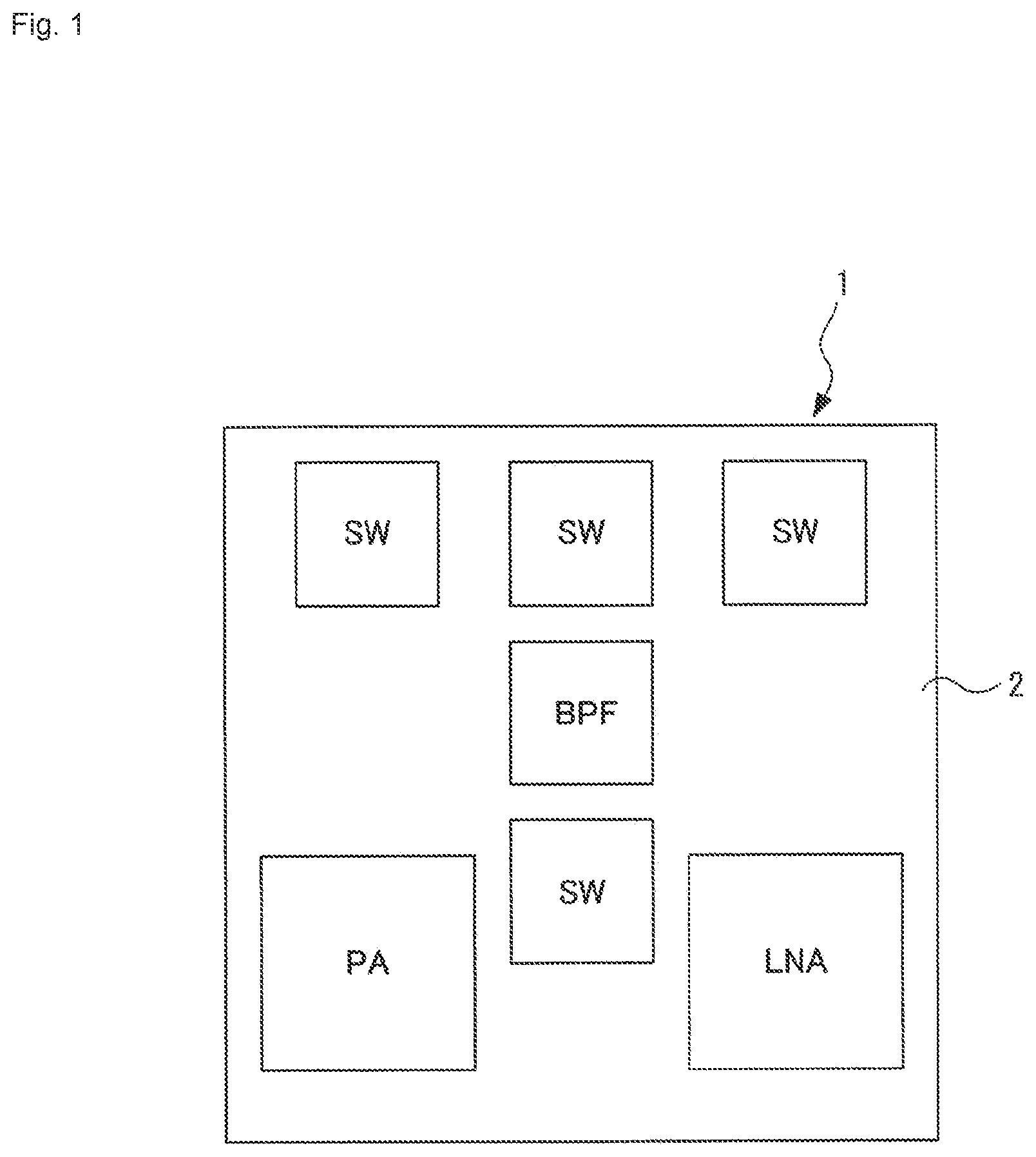
As shown in , a semiconductor device 1 according to the first embodiment of the present technology is mainly composed of a semiconductor chip 2 having a rectangular two dimensional planar shape when viewed in a plan view. The semiconductor chip 2 includes a high frequency power amplifier part PA, a high frequency low noise amplifier part LNA, a high frequency filter part BPF and a high frequency switch part SW. In the high frequency switch part SW, as an element constituting a high frequency switch, a first field effect transistor Q 1 shown in , and is mounted. In the high frequency power amplifier part PA, as an element constituting a high frequency power amplifier, a second field effect transistor Q 2 shown in , and is mounted.
The first field effect transistor Q 1 and the second field effect transistor Q 2 have different planar sizes, and the planar size of the second field effect transistor Q 2 is larger than the planar size of the first field effect transistor Q 1 . Specifically, as shown in and , a separation distance L 2 between a pair of second main electrodes 16 B and 17 B functioning as a source electrode and a drain electrode of the second field effect transistor Q 2 is longer than a separation distance L 1 between a pair of first main electrodes 16 A and 17 A functioning as a source electrode and a drain electrode of the first field effect transistor Q 1 .
As shown in , and , the semiconductor chip 2 includes a semiconductor substrate 10 and an insulating layer 20 provided on the main surface of the semiconductor substrate 10 .
The semiconductor substrate 10 includes a substrate 11 , a buffer layer 11 a provided on the substrate 11 , a channel layer 12 provided on the buffer layer 11 a , and a barrier layer 13 provided on the channel layer 12 . Here, on the main surface of the semiconductor substrate 10 , a first active region 10 A and a second active region 10 B which are partitioned by an inactive region 15 and are insulated and separated from each other are provided. The inactive region 15 is composed of, for example, an impurity diffusion region into which boron (B + ) ions are diffused as impurities. Here, as shown in and , the inactive region 15 is formed deeper than a two dimensional electron gas (2DEG) layer 14 to be described below in a depth direction from the main surface of the semiconductor substrate 10 . Insulation separation (element separation) between the active regions may be performed by a method other than ion implantation. For example, the channel layer 12 may be divided by dry etching and insulation separation between the active regions may be performed.
The substrate 11 is composed of a semiconductor material. Such a substrate 11 is composed of, for example, a Group III-V compound semiconductor material. Regarding the substrate 11 , for example, a semi-insulating single crystal GaN (gallium nitride) substrate is used. A substrate material having a lattice constant different from a lattice constant of the channel layer 12 can be used for the substrate 11 . Examples of such a material constituting the substrate 11 include SiC (silicon carbide), sapphire and Si (silicon). In this case, the lattice constant is adjusted by the buffer layer 11 a between the substrate 11 and the channel layer 12 . The buffer layer 11 a is composed of, for example, a compound semiconductor layer epitaxially grown on the substrate 11 , and is composed using a compound semiconductor having favorable lattice matching to the substrate 11 . For example, on the substrate 11 composed of a single crystal GaN substrate, an epitaxially grown layer of u − GaN (u − indicates that no impurities are added; the same applies hereinafter) to which no impurities are added is provided. When the lattice constant of the substrate 11 is different from the lattice constant of the channel layer 12 , if the buffer layer 11 a is provided between the substrate 11 and the channel layer 12 , it is possible to improve the crystalline state of the channel layer 12 and prevent warping of the wafer. For example, when the substrate 11 is composed of Si and the channel layer 12 is composed of GaN, for example, AlN (aluminum nitride), AlGaN (aluminum gallium nitride) or GaN can be used for the buffer layer 11 a . The buffer layer 11 a may be composed of a single layer or may have a laminated structure. When the buffer layer 11 a is composed of a three dimensional material, each composition may gradually change in the buffer layer 11 a.
The channel layer 12 between the buffer layer 11 a and the barrier layer 13 is a current passage between the source electrode and the drain electrode. Carriers are accumulated in the channel layer 12 due to polarization with respect to the barrier layer 13 , and the two dimensional electron gas (2DEG: Two Dimensional Electron gas) layer 14 is provided in the vicinity of a bonding surface (hetero bonding interface) with respect to the barrier layer 13 . It is preferable that such a channel layer 12 be composed of a compound semiconductor material in which carriers are easily accumulated by polarization with respect to the barrier layer 13 . For example, the channel layer 12 is composed of GaN epitaxially grown on the buffer layer 11 a . The channel layer 12 may be composed of u − GaN to which no impurities are added. In the channel layer 12 composed of u − GaN, since distribution of impurities of carriers in the channel layer 12 is restricted, it is possible to improve the mobility of carriers.
As shown in , and , the insulating layer 20 includes a first insulating film 21 provided on the main surface of the semiconductor substrate 10 , a second insulating film 22 provided on the first insulating film 21 , and a third insulating film 26 provided on the second insulating film 22 . As the first insulating film 21 , for example, an aluminum oxide (Al 3 O 2 ) film is used. As the second insulating film 22 , for example, a silicon oxide (SiO 2 ) film having a high etching selectivity with respect to the first insulating film 21 is used. The first insulating film 21 and the second insulating film 22 are formed with, for example, a film thickness of about 50 nm.
The third insulating film 26 is formed to cover the first insulating film 21 , the second insulating film 22 , and the main surface (the barrier layer 13 ) of the semiconductor substrate 10 in a first cavity part 25 A 1 and a second cavity part 25 B 1 to be described below. The third insulating film 26 has an insulating property with respect to the barrier layer 13 , the first insulating film 21 and the second insulating film 22 exposed to the first cavity part 25 A 1 and the second cavity part 25 B 1 , protects the barrier layer 13 from impurities such as ions, and is formed of a material that forms a favorable interface with the barrier layer 13 and prevents deterioration of device characteristics. For example, the third insulating film 26 is formed of a laminated film in which an Al 2 O 3 film and a hafnium oxide (HfO 2 ) film having a film thickness of about 10 nm are laminated in that order from the side of the main surface of the semiconductor substrate 10 . The third insulating film 26 may be formed of a single Al 2 O 3 film or HfO 2 film.
As shown in , and , the first field effect transistor Q 1 is formed in the first active region 10 A of the main surface of the semiconductor substrate 10 . The first field effect transistor Q 1 includes the buffer layer 11 a , the channel layer 12 , the barrier layer 13 , and the two dimensional electron gas layer 14 . In addition, the first field effect transistor Q 1 includes the pair of first main electrodes 16 A and 17 A which are separated from each other and provided on the first active region 10 A of the main surface of the semiconductor substrate 10 and function as the source electrode and the drain electrode, and the first cavity part 25 A 1 provided in the insulating layer 20 between the pair of first main electrode 16 A and first main electrode 17 A. In addition, the first field effect transistor Q 1 includes a first gate electrode 31 A which has a head part 31 a 1 positioned on the insulating layer 20 and a body part 31 a 2 that penetrates the insulating layer 20 from the head part 31 a 1 and protrudes toward the first cavity part 25 A 1 , and in which the head part 31 a 1 is wider than the body part 31 a 2 . That is, the first field effect transistor Q 1 of the first embodiment is a GaN-based hetero FET (HFET: Hetero Field Effect Transistor).
As shown in , the first gate electrode 31 A has a long shape when viewed in a plan view, and the gate width (Wg) is longer than the gate length (Lg). Here, the first gate electrode 31 A extends over the first active region 10 A and the inactive region 15 . Here, as shown in and , in the first gate electrode 31 A, the head part 31 a 1 is positioned on the third insulating film 26 , and the body part 31 a 2 integrated with the head part 31 a 1 protrudes toward the first cavity part 25 A 1 through a first gate opening 27 A 1 provided in the insulating layer 20 .
As shown in , and , the pair of first main electrodes 16 A and 17 A with the first gate electrode 31 A therebetween are separated from each other in the gate length direction of the first gate electrode 31 A (the short direction and the width direction of the first gate electrode 31 A). Here, the pair of first main electrodes 16 A and 17 A extend over the first active region 10 A and the inactive region 15 in the gate width direction of the first gate electrode 31 A (the longitudinal direction and the length direction of the first gate electrode 31 A).
As shown in , the plane pattern of the first cavity part 25 A 1 when viewed in a plan view is a circular plane pattern surrounding the body part 31 a 2 of the first gate electrode 31 A. Therefore, as shown in , the first cavity part 25 A 1 includes a first part 25 A 1 -L positioned on one side (left side) of the body part 31 a 2 and a second part 25 A 1 -R positioned on the other side (right side) of the body part 31 a 2 in the gate length direction of the first gate electrode 31 A. Here, in the first embodiment, the first cavity part 25 A 1 has a bilaterally symmetrical configuration in which the first part 25 A 1 -L and the second part 25 A 1 -R have substantially the same width. In the gate length direction of the first gate electrode 31 A, the first cavity part 25 A 1 is wider than the body part 31 a 2 of the first gate electrode 31 A and the first gate opening 27 A 1 .
As shown in , and , the second field effect transistor Q 2 is formed in the second active region 10 B different from the first active region 10 A of the main surface of the semiconductor substrate 10 . The second field effect transistor Q 2 includes the buffer layer 11 a , the channel layer 12 , the barrier layer 13 , and the two dimensional electron gas layer 14 . In addition, the second field effect transistor Q 2 includes the pair of second main electrodes 16 B and 17 B which are separated from each other and provided on the second active region 10 B of the main surface of the semiconductor substrate 10 and in which the separation distance L 2 (refer to and ) is longer than the separation distance L 1 (refer to and ) between the pair of first main electrodes 16 A and 17 A of the first field effect transistor Q 1 , and the second cavity part 25 B 1 provided in the insulating layer 20 between the pair of second main electrodes 16 B and 17 B. The pair of second main electrodes 16 B and 17 B function as a source electrode and a drain electrode. In addition, the second field effect transistor Q 2 includes a second gate electrode 31 B which has a head part 31 b 1 positioned on the insulating layer 20 and a body part 31 b 2 that penetrates the insulating layer 20 from the head part 31 b 1 and protrudes toward the second cavity part 25 B 1 , and in which the head part 31 b 1 is wider than the body part 31 b 2 . That is, the second field effect transistor Q 2 of the first embodiment is also a GaN-based hetero FET like the first field effect transistor Q 1 .
As shown in , the second gate electrode 31 B has a long shape when viewed in a plan view, and the gate width is longer than the gate length. Here, the second gate electrode 31 B extends over the second active region 10 B and the inactive region 15 . Here, in the second gate electrode 31 B, the head part 31 b 1 is positioned on the third insulating film 26 , and the body part 31 b 2 integrated with the head part 31 b 1 protrudes toward the second cavity part 25 B 1 through a second gate opening 27 B 1 provided in the insulating layer 20 .
As shown in , and , the pair of second main electrodes 16 B and 17 B with the second gate electrode 31 B therebetween are separated from each other in the gate length direction (the short direction and the width direction of the second gate electrode 31 B) of the second gate electrode 31 B. Here, the pair of second main electrodes 16 B and 17 B extend over the second active region 10 B and the inactive region 15 in the gate width direction of the second gate electrode 31 B (the longitudinal direction and the length direction of the second gate electrode 31 B).
As shown in , the plane pattern of the second cavity part 25 B 1 when viewed in a plan view is a circular plane pattern surrounding the body part 31 b 2 of the second gate electrode 31 B. Therefore, like the first cavity part 25 A 1 , as shown in , the second cavity part 25 B 1 also includes a first part 25 B 1 -L positioned on one side (left side) of the body part 31 b 2 and a second part 25 B 1 -R positioned on the other side (right side) of the body part 31 b 2 in the gate length direction of the second gate electrode 31 B. In the first embodiment, although not limited to this, the second cavity part 25 B 1 has a bilaterally symmetrical configuration in which the first part 25 B 1 -L and the second part 25 B 1 -R have substantially the same width.
The second cavity part 25 B 1 is wider than the body part 31 b 2 of the second gate electrode 31 B and the second gate opening 27 B 1 in the gate length direction of the second gate electrode 31 B. Here, as shown in , the width W 2 of the second cavity part 25 B 1 is wider than the width W 1 of the first cavity part 25 A 1 . That is, the second cavity part 25 B 1 is wider than the first cavity part 25 A 1 .
Here, the width W 2 of the second cavity part 25 B 1 is a length of the second gate electrode 31 B in the gate length direction, and the width W 1 of the first cavity part 25 A 1 is a length of the first gate electrode 31 A in the gate length direction. In the first embodiment, although not limited to this, the first gate electrode 31 A and the second gate electrode 31 B extend in the same direction, and as shown in , respective short directions of the first gate electrode 31 A and the second gate electrode 31 B are the same direction.
The inside of each of the first cavity part 25 A 1 and the second cavity part 25 B 1 is filled with an inert gas or is in a vacuum state, and is a low-dielectric-constant region having a lower dielectric constant than the surrounding first insulating film 21 , second insulating film 22 and third insulating film 26 .
As shown in , the first gate electrode 31 A and the second gate electrode 31 B are provided on the third insulating film 26 . The first gate electrode 31 A and the second gate electrode 31 B are composed of, for example, a laminated film in which a nickel (Ni) film and a gold (Au) film are sequentially laminated from the side of the semiconductor substrate 10 .
The pair of first main electrodes 16 A and 17 A are ohmic-bonded to the barrier layer 13 in the first active region 10 A. The pair of second main electrodes 16 B and 17 B are ohmic-bonded to the barrier layer 13 in the second active region 10 B. The pair of first main electrodes 16 A and 17 A and the pair of second main electrodes 16 B and 17 B are composed of, for example, a laminated film in which a titanium (Ti) film, an Al film, a Ni film, and an Au film are sequentially laminated from the side of the semiconductor substrate 10 .
For example, when the first and second field effect transistors Q 1 and Q 2 are of a depression type in which the threshold voltage is a negative voltage, if a gate voltage Vg is applied to the gate electrodes 31 A and 31 B, the number of carriers in a carrier-deficient region in the surface layer part of the channel layer 12 directly below the gate electrodes 31 A and 31 B decreases, the number of electrons in the channel layer 12 decreases, and the drain current Id hardly flows. Here, if a positive gate voltage Vg is applied to the gate electrodes 31 A and 31 B, the carrier-deficient region disappears, the number of electrons in a buffer layer 12 increases, and the drain current Id is modulated.
As described above, in the semiconductor device 1 according to the first embodiment, the first field effect transistor Q 1 and the second field effect transistor Q 2 having a larger planar size than the first field effect transistor Q 1 are mounted together on the same semiconductor substrate 10 . Here, as shown in , since the first field effect transistor Q 1 includes the first cavity part 25 A 1 , compared with a conventional field effect transistor which has the same planar size as the first field effect transistor Q 1 and does not include the first cavity part 25 A 1 , it is possible to reduce the parasitic capacitance Cgs added between the first gate electrode 31 A and one first main electrode 16 A (for example, a source electrode), and the parasitic capacitance Cgd added between the first gate electrode 31 A and the other first main electrode 17 A (for example, a drain electrode), and thereby it is possible to reduce the on-resistance and improve the isolation characteristics. Here, as shown in , since the second field effect transistor Q 2 includes the second cavity part 25 B 1 wider than the first cavity part 25 A 1 , compared with a conventional field effect transistor which has the same planar size as the second field effect transistor Q 2 and includes a cavity part having the same width as the first cavity part 25 A 1 , it is possible to reduce the parasitic capacitance Cgs added between the second gate electrode 31 B and one second main electrode 16 B (for example, a source electrode) and the parasitic capacitance Cgd added between the second gate electrode 31 B and the other second main electrode 17 B (for example, a drain electrode), and thereby it is possible to reduce the on-resistance and improve high frequency characteristics. Therefore, according to the semiconductor device 1 of the first embodiment, it is possible to reduce the on-resistance of the first field effect transistor Q 1 and the second field effect transistor Q 2 which have different planar sizes, and improve characteristics according to each application.
In addition, the first field effect transistor Q 1 is used as an element constituting the high frequency switch part SW. In this case, according to the first field effect transistor Q 1 , the planar size is reduced by reducing the separation distance L 1 between the pair of first main electrodes 16 A and 17 A, and thus the on-resistance can be reduced, and it is possible to improve high frequency characteristics. On the other hand, the second field effect transistor Q 2 is used as an element constituting the high frequency power amplifier part PA. In this case, in the second field effect transistor Q 2 , it is necessary to increase the separation distance L 2 between the pair of second main electrodes 16 B and 17 B and increase a device withstand voltage (withstand voltage between gate/drain), and the planar size is larger than that of the first field effect transistor Q 1 . Therefore, like the semiconductor device 1 of the first embodiment, when the second cavity part 25 B 1 of the second field effect transistor Q 2 is made wider than the first cavity part 25 A 1 of the first field effect transistor Q 1 , it is possible to secure the device withstand voltage of the second field effect transistor Q 2 and reduce the on-resistance.
Here, a wiring layer and other insulating layers are provided above the insulating layer 20 , but in , and , the wiring layer and other insulating films above the insulating layer 20 are not shown.
In addition, in the first embodiment, the first field effect transistor Q 1 and the second field effect transistor Q 2 are arranged so that respective short directions of the gate electrodes 31 A and 31 B are the same direction, but respective short directions of the gate electrodes 31 A and 31 B may be different directions.
<Method of Producing Semiconductor Device>
Next, a method of producing the semiconductor device 1 will be described with reference to A, 7 B, 8 A, 8 B, 9 A, 9 B, 10 A, 10 B, 11 A, 11 B, 12 A, 12 B, 13 A, 13 B, 14 A, 14 B, 15 A, and 15 B . A, 8 A, 9 A, 10 A, 11 A, 12 A, 13 A, 14 A and 15 A show processes of forming the first field effect transistor Q 1 in the first active region 10 A of the semiconductor substrate 10 . B, 8 B, 9 B, 10 B, 11 B, 12 B, 13 B, 14 B and 15 B show processes of forming the second field effect transistor Q 2 in the second active region 10 B of the semiconductor substrate 10 . The first field effect transistor Q 1 and the second field effect transistor Q 2 are formed by the same process.
First, as shown in A and 7 B , the semiconductor substrate 10 is prepared. The semiconductor substrate 10 has a laminated structure in which the buffer layer 11 a , the channel layer 12 and the barrier layer 13 are laminated in that order on the substrate 11 . Here, the two dimensional electron gas layer 14 is provided in the vicinity of the bond interface between the channel layer 12 and the barrier layer 13 .
Next, as shown in A and 8 B , on the main surface of the semiconductor substrate 10 , the inactive region 15 that partitions and insulated and separates the first active region 10 A and the second active region 10 B is formed, and also, the pair of first main electrodes 16 A and 17 A that function as a source electrode and a drain electrode are formed on the first active region 10 A of the main surface of the semiconductor substrate 10 , and the pair of second main electrodes 16 B and 17 B that function as a source electrode and a drain electrode are formed on the second active region 10 B of the main surface of the semiconductor substrate 10 .
The inactive region 15 is formed by selectively injecting, for example, boron (B+) ions as impurities ions, into the surface layer part on the side of the main surface of the semiconductor substrate 10 , and then performing a heat treatment in order to activate the injected B+ ions.
The pair of first main electrodes 16 A and 17 A and the pair of second main electrodes 16 B and 17 B are formed when a conductive film having a multi-layer structure is formed by sequentially laminating, for example, a Ti film, an Al film, a Ni film, and an Au film from the side of the semiconductor substrate 10 , on the entire main surface of the semiconductor substrate 10 including the first active region 10 A and the second active region 10 B by a CVD method or a sputtering method, and the conductive film is then patterned using a well-known photolithography technique and a dry etching technique having high directivity. The pair of first main electrodes 16 A and 17 A are formed in a long shape, and are formed apart from each other in the short direction (width direction) orthogonal to the longitudinal direction. The pair of second main electrodes 16 B and 17 B are also formed in a long shape, and are formed apart from each other in the short direction (width direction) orthogonal to the longitudinal direction. Here, the pair of second main electrodes 16 B and 17 B between which the separation distance L 2 is longer than the separation distance L 1 between the pair of first main electrodes 16 A and 17 A is formed apart from each other.
Next, as shown in A and 9 B , the first insulating film 21 is formed on the entire main surface of the semiconductor substrate 10 including the above first active region 10 A and second active region 10 B, and then, as shown in A and 9 B , the second insulating film 22 is formed on the entire main surface of the semiconductor substrate 10 including the above first active region 10 A and second active region 10 B with the first insulating film 21 therebetween. The second insulating film 22 is formed of an insulating film having a high etching selectivity with respect to the first insulating film 21 . In other words, the first insulating film 21 is formed of an insulating film having a low etching selectivity with respect to the second insulating film 22 . For example, an aluminum oxide (Al2O3) film is filmed as the first insulating film 21 by an atomic vapor deposition (ALD) method, and a silicon oxide (SiO2) film is formed as the second insulating film 22 by a chemical vapor deposition (CVD) method.
According to this process, the first active region 10 A and the second active region 10 B of the main surface of the semiconductor substrate 10 are covered with the first insulating film 21 and the second insulating film 22 .
Next, as shown in A and 10 B , a first opening 24 A 1 is formed in the second insulating film 22 on the first active region 10 A of the main surface of the semiconductor substrate 10 , and a second opening 24 B 1 is formed in the second insulating film 22 on the second active region 10 B of the main surface of the semiconductor substrate 10 . The first opening 24 A 1 and a second opening 24 B 1 are formed by selectively etching the second insulating film 22 using a well-known photolithography technique and well-known dry etching having high directivity as an anisotropic etching technique.
The first opening 24 A 1 is formed between the pair of first main electrode 16 A and first main electrode 17 A in a plan view, and are formed with a long plane pattern in the longitudinal direction of the pair of first main electrodes 16 A and 17 A. The second opening 24 B 1 is formed between the pair of second main electrode 16 B and second main electrode 17 B in a plan view, and are formed with a long plane pattern that extends in the longitudinal direction of the pair of second main electrodes 16 B and 17 B.
Next, as shown in A and 11 B , the first cavity part 25 A 1 wider than the first opening 24 A 1 is formed by etching the first insulating film 21 on the first active region 10 A of the semiconductor substrate 10 through the first opening 24 A 1 , and the second cavity part 25 B 1 wider than the second opening 24 B 1 is formed by etching the first insulating film 21 on the second active region 10 B of the semiconductor substrate 10 through the second opening 24 B 1 .
The first cavity part 25 A 1 and the second cavity part 25 B 1 are formed by etching the first insulating film 21 by performing isotropic wet etching with less damage on the main surface of the semiconductor substrate 10 , that is, the surface of the barrier layer 13 . Wet etching of the first insulating film 21 is performed under conditions in which an etching selectivity with respect to the second insulating film 22 is obtained. That is, etching is performed under conditions in which a wet etching rate is higher for the first insulating film 21 than for the second insulating film 22 . A higher selectivity is more preferable, but for example, etching is performed under conditions in which the etching selectivity between the first insulating film 21 and the second insulating film 22 is 10 or more:1.
Next, as shown in A and 12 B , a mask RM 1 is formed to cover the first opening 24 A 1 on the first active region 10 A of the semiconductor substrate 10 except for the second opening 24 B 1 on the second active region 10 B of the semiconductor substrate 10 . The mask RM 1 is formed by forming a photosensitive resist film on the entire main surface of the semiconductor substrate 10 including the above first active region 10 A and second active region 10 B and then subjecting the photosensitive resist film to a photosensitivity and developing treatment or the like to form a predetermined pattern.
Next, as shown in A and 13 B , the mask RM 1 is used as an etching mask, and the width of the second cavity part 25 B 1 is extended by selectively etching the first insulating film 21 through the second opening 24 B 1 when the first opening 24 A 1 is covered with the mask RM 1 . The extension of the second cavity part 25 B 1 is performed by etching the first insulating film 21 by performing isotropic wet etching with less damage on the main surface of the semiconductor substrate 10 , that is, the surface of the barrier layer 13 . Wet etching of the first insulating film 21 is performed under conditions in which an etching selectivity with respect to the second insulating film 22 is obtained. For example, etching is performed under conditions in which the etching selectivity between the first insulating film 21 and the second insulating film 22 is 10 or more:1.
According to this process, the second cavity part 25 B 1 having a width W 2 (refer to ) wider than the width W 1 (refer to ) of the first cavity part 25 A 1 is formed
In addition, in this process, since the width of the second cavity part 25 B 1 is selectively extended, the first insulating film 21 can remain between each of the pair of first main electrodes 16 A and 17 A and the first cavity part 25 A 1 , and the first insulating film 21 can remain between each of the pair of second main electrodes 16 B and 17 B and the second cavity part 25 B 1 .
Next, after the mask RM 1 is removed, as shown in A and 14 B , in the first cavity part 25 A 1 and the second cavity part 25 B 1 , the third insulating film 26 that covers the first insulating film 21 , the second insulating film 22 , and the main surface of the semiconductor substrate 10 (the surface of the barrier layer 13 ), covers respective side walls in the first opening 24 A 1 and the second opening 24 B 1 of the second insulating film 22 , and covers the second insulating film 22 is formed. The third insulating film 26 is formed by, for example, forming an Al2O3 film using an ALD method. Since the ALD method allows uniform film formation, the exposed surface of the barrier layer 13 , the first insulating film 21 and the second insulating film 22 is covered with the uniform third insulating film 26 .
In this process, the insulating layer 20 including the first insulating film 21 , the second insulating film 22 and the third insulating film 26 is formed on the first active region 10 A and the second active region 10 B of the semiconductor substrate 10 .
In addition, in this process, since respective side walls in the first opening 24 A 1 and the second opening 24 B 1 of the second insulating film 22 are covered with the third insulating film 26 , the first gate opening 27 A 1 having a narrower opening width than the first opening 24 A 1 is formed, and the second gate opening 27 B 1 having a narrower opening width than the second opening 24 B 1 is formed.
In addition, in this process, the first cavity part 25 A 1 and the second cavity part 25 B 1 are surrounded by the third insulating film 26 . Here, since the third insulating film 26 is formed with an almost uniform film thickness, in the first cavity part 25 A 1 and the second cavity part 25 B 1 surrounded by the third insulating film 26 , the width W 2 (refer to ) of the second cavity part 25 B 1 is wider than the width W 1 (refer to ) of the first cavity part 25 A 1 .
Next, as shown in A and 15 B , a gate material 30 is formed on the entire surface of the third insulating film 26 including the above first active region 10 A and second active region 10 B of the semiconductor substrate 10 . The gate material 30 is formed by sequentially laminating, for example, a Ni film and an Au film from the side of the semiconductor substrate 10 by a vapor deposition method.
In this process, the inside of the first gate opening 27 A 1 and the inside of the second gate opening 27 B 1 are filled with the gate material 30 , and the gate material 30 is selectively filled into a part directly below the first gate opening 27 A 1 in the first cavity part 25 A 1 and a part directly below the second gate opening 27 B 1 in the second cavity part 25 B 1 .
Next, the gate material 30 is patterned using a well-known photolithography technique and a dry etching technique having high directivity, the first gate electrode 31 A (refer to ) is formed on the first active region 10 A of the semiconductor substrate 10 , and the second gate electrode 31 B (refer to ) is formed on the second active region 10 B of the semiconductor substrate 10 . Here, each of the first gate electrode 31 A and the second gate electrode 31 B may be formed by a lift-off method.
In this process, the first gate electrode 31 A includes the head part 31 a 1 positioned on the insulating layer 20 and the body part 31 a 2 that penetrates the insulating layer 20 from the head part 31 a 1 and protrudes toward the first cavity part 25 A 1 , and the head part 31 a 1 is formed wider than the body part 31 a 2 . Similarly, the second gate electrode 31 B includes the head part 31 b 1 positioned on the insulating layer 20 and the body part 31 b 2 that penetrates the insulating layer 20 from the head part 31 b 1 and protrudes toward the second cavity part 25 B 1 , and the head part 31 b 1 is formed wider than the body part 31 b 2 .
In addition, in this process, the first cavity part 25 A 1 is formed bilaterally symmetrically with almost the same cavity width on both sides of the first gate electrode 31 A in the gate length direction. In addition, the second cavity part 25 B 1 is formed bilaterally symmetrical with almost the same cavity width on both sides of the second gate electrode 31 B in the gate length direction.
According to this process, the first field effect transistor Q 1 shown in , and is almost completed, and the second field effect transistor Q 2 shown in , and is almost completed.
Then, a wiring layer and other insulating layers are formed on the insulating layer 20 , and thus the semiconductor device 1 shown in to is almost completed.
According to the method of producing the semiconductor device 1 of the first embodiment, the first cavity part 25 A 1 and the second cavity part 25 B 1 wider than the first cavity part 25 A 1 can be formed by the same process.
In addition, according to the method of producing the semiconductor device 1 of the first embodiment, since the width of the second cavity part 25 B 1 of the second field effect transistor Q 2 having a larger planar size than the first field effect transistor Q 1 is selectively extended, in the first field effect transistor Q 1 , the first insulating film 21 can remain between each of the pair of first main electrodes 16 A and 17 A and the first cavity part 25 A 1 , and thus the first field effect transistor Q 1 including the first cavity part 25 A 1 and the second field effect transistor Q 2 including the second cavity part 25 B 1 wider than the first cavity part 25 A 1 and having a larger planar size than the first field effect transistor Q 1 can be formed by the same process.
In addition, according to the method of producing the semiconductor device 1 of the first embodiment, in the first field effect transistor Q 1 , since the first insulating film 21 can remain between each of the pair of first main electrodes 16 A and 17 A and the first cavity part 25 A 1 , the planar size of the first field effect transistor Q 1 can be made smaller than that of the second field effect transistor Q 2 . Thereby, it is possible to reduce the on-resistance of the first field effect transistor Q 1 and improve high frequency characteristics, and reduce the size of the semiconductor device 1 .
In addition, in the method of producing the semiconductor device 1 according to the first embodiment, since the first insulating film 21 is etched by wet etching, it is possible to prevent damage to the main surface of the semiconductor substrate 10 (the barrier layer 13 ). Specifically, since the main surface of the semiconductor substrate 10 is not exposed to plasma, and ions and the like in an etching gas do not enter the semiconductor substrate 10 during etching, deterioration of the on-resistance, that is, an increase in the sheet resistance, and deterioration of off characteristics, that is, an increase in the leakage current or a decrease in the withstand voltage, are not caused.
Second Embodiment
<Configuration of Semiconductor Device>
A semiconductor device 1 A according to a second embodiment of the present technology basically has the same configuration as the semiconductor device 1 of the above first embodiment, and includes a second field effect transistor Q 3 in place of the second field effect transistor Q 2 of the first embodiment.
That is, as shown in A and 16 B , the semiconductor device 1 A according to the second embodiment of the present technology includes the first field effect transistor Q 1 formed in the first active region 10 A of the main surface of the semiconductor substrate 10 (refer to A ) and the second field effect transistor Q 3 formed in the second active region 10 B of the main surface of the semiconductor substrate 10 (refer to B ). Here, as shown in B , the second field effect transistor Q 3 includes a second cavity part 25 B 2 in place of the second cavity part 25 B 1 of the second field effect transistor Q 2 of the first embodiment. The other configurations are the same as those in the above first embodiment.
Like the second cavity part B 1 of the above first embodiment, the plane pattern of the second cavity part 25 B 2 of the second field effect transistor Q 3 when viewed in a plan view is a circular plane pattern surrounding the body part 31 b 2 of the second gate electrode 31 B. Therefore, like the second cavity part 25 B 1 of the above first embodiment, as shown in B , the second cavity part 25 B 2 includes a first part 25 B 2 -L positioned on one side (left side) of the body part 31 b 2 of the second gate electrode 31 B and a second part 25 B 2 -R positioned on the other side (right side) of the body part 31 b 2 of the second gate electrode 31 B in the gate length direction of the second gate electrode 31 B. Here, unlike the second cavity part 25 B 1 of the above first embodiment, in the second embodiment, the second cavity part 25 B 2 has a bilaterally asymmetrical configuration in which the width of the second part 25 B 2 -R is wider than the width of the first part 25 B 2 -L.
In the gate length direction (longitudinal direction) of the second gate electrode 31 B, the second cavity part 25 B 2 is wider than the body part 31 b 2 of the second gate electrode 31 B and the second gate opening 27 B 1 . Here, the width W 2 of the second cavity part 25 B 2 is wider than the width W 1 of the first cavity part 25 A 1 . That is, the second cavity part 25 B 2 is wider than the first cavity part 25 A 1 .
According to the semiconductor device 1 A according to the second embodiment, the same effects as those of the semiconductor device 1 according to the first embodiment described above can be obtained.
In addition, for example, when reduction in the source resistance is important for the device characteristics, in the second field effect transistor Q 3 , when one second main electrode 16 B is used as a drain electrode, if the separation distance between one second main electrode 16 B and the second gate electrode 31 B increases, the source resistance increases and the device characteristics deteriorate. Here, when the width of the second cavity part 25 B 2 -R on the side of the other second main electrode 16 B that functions as a drain electrode is widened, while the source resistance is kept low, an effect of reducing the parasitic capacitance (Cgd) added between the gate electrode and the other main electrode can be improved.
Here, a wiring layer and other insulating layers are provided above the insulating layer 20 , but in A and 16 B , the wiring layer and other insulating films above the insulating layer 20 are not shown.
<Method of Producing Semiconductor Device>
Next, a method of producing the semiconductor device 1 A according to the second embodiment will be described with reference to A, 17 B, 18 A, 18 B, 19 A, 19 B, 20 A, and 20 B . A, 18 A, 19 A and 20 A show processes of forming the first field effect transistor Q 1 in the first active region 10 A of the semiconductor substrate 10 . B, 18 B, 19 B and 20 B show processes of forming the second field effect transistor Q 3 in the second active region 10 B of the semiconductor substrate 10 . The first field effect transistor Q 1 and the second field effect transistor Q 3 are formed by the same process.
First, the same processes as the processes shown in A, 7 B, 8 A, 8 B, 9 A, 9 B, 10 A, and 10 B in the first embodiment are performed, and as shown in A and 17 B , the pair of first main electrodes 16 A and 17 A, the pair of second main electrodes 16 B and 17 B, the first insulating film 21 and the second insulating film 22 , the first opening 24 A 1 and the second opening 24 B 1 and the like are formed.
Next, the same processes as the processes shown in A and 11 B in the above first embodiment are performed, and as shown in A and 17 B , the first cavity part 25 A 1 wider than the first opening 24 A 1 is formed, and the second cavity part 25 B 2 wider than the second opening 24 B 1 is formed.
Next, as shown in A and 18 B , a mask RM 2 that covers the first opening 24 A 1 on the first active region 10 A of the semiconductor substrate 10 and covers a part of each of the second opening 24 B 1 and the second cavity part 25 B 2 on the second active region 10 B of the semiconductor substrate 10 in the width direction is formed. That is, the mask RM 2 in which the side wall of the opening end is separated from one side wall between both side walls of each of the second opening 24 B 1 and the second cavity part 25 B 2 in the width direction is formed on the second active region 10 B. Like the mask RM 1 of the above first embodiment, the mask RM 2 is formed by forming a photosensitive resist film on the entire main surface of the semiconductor substrate 10 including the above first active region 10 A and second active region 10 B, and then subjecting the photosensitive resist film to a photosensitivity and developing treatment or the like to form a predetermined pattern.
Next, the mask RM 2 is used as an etching mask, and as shown in A and 19 B , and the width of the second cavity part 25 B 2 is extended by etching the first insulating film 21 through the space between the side wall of the mask RM 2 and the side wall in the second opening 24 B 1 of the second insulating film 22 when the first opening 24 A 1 is covered with the mask RM 2 and a part of each of the second opening 24 B 1 and the second cavity part 25 B 2 in the width direction is covered with the mask RM 2 . Like the extension of the second cavity part 25 B 2 in the above first embodiment, the extension of the second cavity part 25 B 2 is performed by etching the first insulating film 21 by performing isotropic wet etching with less damage on the main surface of the semiconductor substrate 10 , that is, the surface of the barrier layer 13 . In addition, wet etching of the first insulating film 21 is performed under conditions in which an etching selectivity with respect to the second insulating film 22 is obtained as in the above second embodiment.
According to this process, the second cavity part 25 B 2 having a width W 2 wider than the width W 1 of the first cavity part 25 A 1 is formed. The width of the second cavity part 25 B 2 extending from the second opening 24 B 1 toward the second main electrode 17 B is formed wider than the width of the second cavity part 25 B 2 extending from the second opening 24 B 1 toward one second main electrode 16 B.
In addition, in this process, since the width of the second cavity part 25 B 2 is extended, the first insulating film 21 can remain between each of the pair of first main electrodes 16 A and 17 A and the first cavity part 25 A 1 , and the first insulating film 21 can remain between each of the pair of second main electrodes 16 B and 17 B and the second cavity part 25 B 1 .
Next, after the mask RM 2 is removed, the processes shown in A and 13 B in the above first embodiment 1 are performed, and as shown in A and 20 B , in the first cavity part 25 A 1 and the second cavity part 25 B 2 , the third insulating film 26 that covers the first insulating film 21 , the second insulating film 22 , and the main surface of the semiconductor substrate 10 (the surface of the barrier layer 13 ), covers respective side walls in the first opening 24 A 1 and the second opening 24 B 1 of the second insulating film 22 , and covers the second insulating film 22 is formed.
In this process, the insulating layer 20 including the first insulating film 21 , the second insulating film 22 and the third insulating film 26 is formed on the first active region 10 A and the second active region 10 B of the semiconductor substrate 10 .
In addition, in this process, since respective side walls in the first opening 24 A 1 and the second opening 24 B 1 of the second insulating film 22 are covered with the third insulating film 26 , the first gate opening 27 A 1 having a narrower opening width than the first opening 24 A 1 is formed, and the second gate opening 27 B 1 having a narrower opening width than the second opening 24 B 1 is formed.
In addition, in this process, the first cavity part 25 A 1 and the second cavity part 25 B 2 are surrounded by the third insulating film 26 . Here, since the third insulating film 26 is formed with an almost uniform film thickness, in the first cavity part 25 A 1 and the second cavity part 25 B 2 surrounded by the third insulating film 26 , the width W 2 (refer to B ) of the second cavity part 25 B 2 is larger than the width W 1 (refer to A ) of the first cavity part 25 A 1 .
Then, the same processes as in the above first embodiment are performed, the first gate electrode 31 A and the second gate electrode 31 B are formed, and thus the first field effect transistor Q 1 shown in A is almost completed, and the second field effect transistor Q 3 shown in B is almost completed.
After that, as in the above first embodiment, a wiring layer and other insulating layers are formed on the insulating layer 20 , and thus the semiconductor device 1 A according to the second embodiment is almost completed.
According to the method of producing the semiconductor device 1 A of the second embodiment, the same effects as in method of producing the semiconductor device 1 according to the first embodiment described above can be obtained.
In addition, according to the method of producing the semiconductor device 1 A of the second embodiment, it is possible to form the bilaterally asymmetrical second cavity part 25 B 2 in which the width of the second part 25 B 2 -R is wider than the width of the first part 25 B 2 -L. Here, the width of the second part 25 B 2 -R of the second cavity part 25 B 2 can be made wider than the width of the second part 25 A 1 -R of the first cavity part 25 A 1 .
In addition, the asymmetrical second cavity part 25 B 2 can be formed with the same number of masks as in the first embodiment.
Third Embodiment
<Configuration of Semiconductor Device>
A semiconductor device 1 B according to a third embodiment of the present technology basically has the same configuration as the semiconductor device 1 of the above first embodiment, and includes a second field effect transistor Q 4 in place of the second field effect transistor Q 2 of the above first embodiment.
That is, as shown in A and 21 B , the semiconductor device 1 B according to the third embodiment of the present technology includes the first field effect transistor Q 1 formed in the first active region 10 A of the main surface of the semiconductor substrate 10 (refer to A ) and the second field effect transistor Q 4 formed in the second active region 10 B of the main surface of the semiconductor substrate 10 (refer to B ). Here, as shown in B , the second field effect transistor Q 4 includes a second cavity part 25 B 3 in place of the second cavity part 25 B 1 of the above second field effect transistor Q 2 of the first embodiment. The other configurations are the same as those in the above first embodiment.
Like the second cavity part 25 B 1 of the above first embodiment, the plane pattern of the second cavity part 25 B 3 of the second field effect transistor Q 4 when viewed in a plan view is a circular plane pattern surrounding the body part 31 b 2 of the second gate electrode 31 B. Therefore, like the second cavity part 25 B 1 of the above first embodiment, as shown in B , the second cavity part 25 B 3 includes a first part 25 B 3 -L positioned on one side (left side) of the body part 31 b 2 of the second gate electrode 31 B and a second part 25 B 3 -R positioned on the other side (right side) of the body part 31 b 2 of the second gate electrode 31 B in the gate length direction of the second gate electrode 31 B. Here, unlike the second cavity part 25 B 1 of the above first embodiment, in the third embodiment, the second cavity part 25 B 3 has a bilaterally asymmetrical configuration in which the width of the second part 25 B 3 -R is wider than the width of the first part 25 B 3 -L. Here, a third opening 27 C 1 provided in the insulating layer 20 is connected to the second part 25 B 3 -R of the second cavity part 25 B 3 .
The second cavity part 25 B 3 is wider than the body part 31 b 2 of the second gate electrode 31 B and the second gate opening 27 B 1 in the gate length direction (longitudinal direction) of the second gate electrode 31 B. Here, the width W 2 of the second cavity part 25 B 3 is wider than the width W 1 of the first cavity part 25 A 1 . That is, the second cavity part 25 B 3 is wider than the first cavity part 25 A 1 .
According to the semiconductor device 1 B according to the third embodiment, the same effects as those of the semiconductor device 1 A according to the second embodiment described above can be obtained.
Here, a wiring layer and other insulating layers are provided above the insulating layer 20 , but in A and 21 B , the wiring layer and other insulating films above the insulating layer 20 are not shown.
<Method of Producing Semiconductor Device>
Next, a method of producing the semiconductor device 1 B according to the third embodiment will be described with reference to A, 22 B, 23 A, 23 B, 24 A , and 24 B. A, 23 A, and 24 A show processes of forming the first field effect transistor Q 1 in the first active region 10 A of the semiconductor substrate 10 , and B, 23 B, and 24 B show processes of forming the second field effect transistor Q 4 in the second active region 10 B of the semiconductor substrate 10 . The first field effect transistor Q 1 and the second field effect transistor Q 4 are formed by the same process.
First, the same processes as the processes shown in A, 7 B, 8 A, 8 B, 9 A, and 9 B in the first embodiment are performed, and as shown in A and 22 B , the pair of first main electrodes 16 A and 17 A, the pair of second main electrodes 16 B and 17 B, the first insulating film 21 and the second insulating film 22 and the like are formed.
Next, as shown in A and 22 B , the first opening 24 A 1 is formed in the second insulating film 22 on the first active region 10 A of the main surface of the semiconductor substrate 10 , and the second opening 24 B 1 and a third opening 24 C 1 adjacent to each other are formed in the second insulating film 22 on the second active region 10 B of the main surface of the semiconductor substrate 10 . The first opening 24 A 1 , the second opening 24 B 1 and the third opening 24 C 1 are formed by etching the second insulating film 22 using a well-known photolithography technique and well-known dry etching having high directivity as an anisotropic etching technique as in the above first embodiment.
The first opening 24 A 1 is formed between the pair of first main electrodes 16 A and 17 A in a plan view, and is formed with a long plane pattern in the longitudinal direction of the pair of first main electrodes 16 A and 17 A. The second opening 24 B 1 and the third opening 24 C 1 are formed between the pair of second main electrodes 16 B and 17 B in a plan view, and are formed with a long plane pattern in the longitudinal direction of the pair of second main electrodes 16 B and 17 B.
Next, as shown in A and 23 B , the first cavity part 25 A 1 wider than the first opening 24 A 1 is formed by etching the first insulating film 21 on the first active region 10 A of the semiconductor substrate 10 through the first opening 24 A 1 , and the second cavity part 25 B 3 wider than the first cavity part 25 A 1 is formed by etching the first insulating film 21 on the second active region 10 B of the semiconductor substrate 10 through the second opening 24 B 1 and the third opening 24 C 1 .
The first cavity part 25 A 1 and the second cavity part 25 B 3 are formed by etching the first insulating film 21 by performing isotropic wet etching with less damage on the main surface of the semiconductor substrate 10 , that is, the surface of the barrier layer 13 . Wet etching of the first insulating film 21 is performed under conditions in which an etching selectivity with respect to the second insulating film 22 is obtained as in the above first embodiment.
In this process, since the first insulating film 21 on the second active region 10 B is etched with an etching solution supplied through two openings (the second opening 24 B 1 and the third opening 2 C 1 ), the second cavity part 25 B 3 having the width W 2 (refer to B ) wider than the width W 1 (refer to A ) of the first cavity part 25 A 1 formed with an etching solution supplied through one opening is formed. In addition, since the third opening 24 C 1 is provided between the second opening 24 B 1 and the other second main electrode 17 B in a plan view, the width of the second cavity part 25 B 3 extending from the second opening 24 B 1 toward the other second main electrode 17 B is formed wider than the width of the second cavity part 25 B 3 extending from the second opening 24 B 1 to one second main electrode 16 B.
Next, the same processes as the processes shown in A and 13 B in the above first embodiment 1 are performed, and as shown in A and 24 B , in the first cavity part 25 A 1 and the second cavity part 25 B 3 , the third insulating film 26 that covers the first insulating film 21 , the second insulating film 22 , and the main surface of the semiconductor substrate 10 (the surface of the barrier layer 13 ), covers respective side walls in the first opening 24 A 1 , the second opening 24 B 1 and the third opening 24 C 1 of the second insulating film 22 , and covers the second insulating film 22 is formed.
In this process, the insulating layer 20 including the first insulating film 21 , the second insulating film 22 and the third insulating film 26 is formed on the first active region 10 A and the second active region 10 B of the semiconductor substrate 10 .
In addition, in this process, since respective side walls in the first opening 24 A 1 and a second opening 24 B 2 of the second insulating film 22 are covered with the third insulating film 26 , the first gate opening 27 A 1 having a narrower opening width than the first opening 24 A 1 is formed, and a second gate opening 27 B 2 having a narrower opening width than the second opening 24 B 1 and the third opening 27 C 1 having a narrower opening width than the third opening 24 C 1 are formed.
In addition, in this process, the first cavity part 25 A 1 and the second cavity part 25 B 3 are surrounded by the third insulating film 26 . Here, since the third insulating film 26 is formed with an almost uniform film thickness, in the first cavity part 25 A 1 and the second cavity part 25 B 3 surrounded by the third insulating film 26 , the width W 2 (refer to B ) of the second cavity part 25 B 3 is wider than the width W 1 (refer to A ) of the first cavity part 25 A 1 .
Then, the same processes as in the above first embodiment are performed, the first gate electrode 31 A and the second gate electrode 31 B are formed, and thus the first field effect transistor Q 1 shown in A is almost completed, and the second field effect transistor Q 4 shown in B is almost completed.
After that, as in the above first embodiment, a wiring layer and other insulating layers are formed on the insulating layer 20 , and thus the semiconductor device 1 according to the second embodiment is almost completed.
According to the method of producing the semiconductor device 1 B of the third embodiment, the same effects as in the method of producing a semiconductor device according to the first embodiment described above can be obtained.
In addition, according to the method of producing the semiconductor device 1 B of the third embodiment, it is possible to form the bilaterally asymmetrical second cavity part 25 B 3 in which the width of the second part 25 B 3 -R is wider than the width of the first part 25 B 3 -L.
In addition, since the second cavity part 25 B 3 wider than the first cavity part 25 A 1 can be formed without using an etching mask, it is possible to reduce the number of production processes as compared with the above first embodiment and second embodiment, and it is possible to reduce the production cost of the semiconductor device 1 B.
Here, in the above third embodiment, two openings (the second opening 24 B 1 and the second opening 24 C 1 ) are formed in the second insulating film 22 on the second active region 10 B, but three or more openings may be formed in the second insulating film 22 on the second active region 10 B. A plurality of openings are arranged at predetermined intervals in the arrangement direction of the pair of second gate electrodes 17 A and 17 B.
Fourth Embodiment
<Configuration of Semiconductor Device>
As shown in A and 25 B , a semiconductor device 1 C according to a fourth embodiment of the present technology includes the semiconductor substrate 10 , a first insulating layer 20 A provided on the first active region 10 A of the main surface of the semiconductor substrate 10 , and a second insulating layer 20 B provided on the second active region 10 B different from the first active region 10 A of the main surface of the semiconductor substrate 10 . In addition, the semiconductor device 1 C includes a first field effect transistor Q 5 formed in the first active region 10 A of the main surface of the semiconductor substrate 10 and a second field effect transistor Q 6 formed in the second active region 10 B of the main surface of the semiconductor substrate 10 . The first field effect transistor Q 5 is an element constituting a high frequency switch of the high frequency switch part SW shown in . The second field effect transistor Q 6 is an element constituting a high frequency power amplifier of the high frequency power amplifier part PA shown in .
As shown in A , the first insulating layer 20 A includes a pair of first etching stopper parts 21 A 1 and 21 A 2 provided on the first active region 10 A of the main surface of the semiconductor substrate 10 , the second insulating film 22 provided on the pair of first etching stopper parts 21 A 1 and 21 A 2 , and the third insulating film 26 provided on the second insulating film 22 .
As shown in B , the second insulating layer 20 B includes a pair of second etching stopper parts 21 B 1 and 21 B 2 provided on the second active region 10 B of the main surface of the semiconductor substrate 10 , the second insulating film 22 provided on the pair of second etching stopper parts 21 B 1 and 21 B 2 , and the third insulating film 26 provided on the second insulating film 22 .
The first insulating film 21 (refer to A and 28 B ) is formed of, for example, an Al 302 film. The pair of first etching stopper parts 21 A 1 and 21 A 2 , and the pair of second etching stopper parts 21 B 1 and 21 B 2 are formed of, for example, a crystallization region in which a heat treatment is performed on the first insulating film 21 (refer to A and 28 B ) to enhance chemical resistance to an etching solution during wet etching. The second insulating film 22 is formed of, for example, a SiO2 film having a high etching selectivity with respect to the first insulating film 21 . The first insulating film 21 is formed with, for example, a film thickness of about 50 nm. The pair of first etching stopper parts 21 A 1 and 21 A 2 , the pair of second etching stopper parts 21 B 1 and 21 B 2 , and the second insulating film 22 are formed with, for example, a film thickness of about 50 nm.
As shown in A , the third insulating film 26 is formed to cover the first insulating film 21 , the second insulating film 22 , and the main surface of the semiconductor substrate 10 (the barrier layer 13 ) in a first cavity part 25 A 2 to be described below. In addition, as shown in B , the third insulating film 26 is formed to cover the first insulating film 21 , the second insulating film 22 , and the main surface of the semiconductor substrate 10 (the barrier layer 13 ) in a second cavity part 25 B 4 to be described below.
As shown in A , the first field effect transistor Q 5 includes the buffer layer 11 a , the channel layer 12 , the barrier layer 13 , and the two dimensional electron gas layer 14 . In addition, the first field effect transistor Q 5 includes the pair of first main electrodes 16 A and 17 A which are separated from each other and provided on the first active region 10 A of the main surface of the semiconductor substrate 10 and function as the source electrode and the drain electrode, and the first cavity part 25 A 2 provided in the first insulating layer 20 A between the pair of first main electrodes 16 A and 17 A. In addition, the first field effect transistor Q 5 includes the first gate electrode 31 A which has the head part 31 a 1 positioned on the first insulating layer 20 A and the body part 31 a 2 that penetrates the first insulating layer 20 A from the head part 31 a 1 and protrudes toward the first cavity part 25 A 2 , and in which the head part 31 a 1 is wider than the body part 31 a 2 . That is, the first field effect transistor Q 5 of the first embodiment is a GaN-based hetero FET.
The first gate electrode 31 A has a long shape when viewed in a plan view, and the gate width is longer than the gate length. Here, the first gate electrode 31 A extends over the first active region 10 A and the inactive region 15 . Here, in the first gate electrode 31 A, the head part 31 a 1 is positioned on the third insulating film 26 , and the body part 31 a 2 integrated with the head part 31 a 1 protrudes toward the first cavity part 25 A 2 through the first gate opening 27 A 1 provided in the first insulating layer 20 A.
The pair of first main electrodes 16 A and 17 A with the first gate electrode 31 A therebetween are separated from each other in the gate length direction of the first gate electrode 31 A. Here, the pair of first main electrodes 16 A and 17 A extend over the first active region 10 A and the inactive region 15 in the gate width direction of the first gate electrode 31 A.
The plane pattern of the first cavity part 25 A 2 when viewed in a plan view is a circular plane pattern surrounding the body part 31 a 2 of the first gate electrode 31 A. Therefore, as shown in A , the first cavity part 25 A 2 includes a first part 25 A 2 -L positioned on one side (left side) of the body part 31 a 2 and a second part 25 A 2 -R positioned on the other side (right side) of the body part 31 a 2 in the gate length direction of the first gate electrode 31 A. Here, in the fourth embodiment, the first cavity part 25 A 2 has a bilaterally symmetrical configuration in which the first part 25 A 2 -L and the second part 25 A 2 -R have substantially the same width. In the gate length direction (longitudinal direction) of the first gate electrode 31 A, the first cavity part 25 A 2 is wider than the body part 31 a 2 of the first gate electrode 31 A and the first gate opening 27 A 1 .
As shown in B , the second field effect transistor Q 6 includes the buffer layer 11 a , the channel layer 12 , the barrier layer 13 , and the two dimensional electron gas layer 14 . In addition, the second field effect transistor Q 6 includes the pair of second main electrodes 16 B and 17 B which are separated from each other and provided on the second active region 10 B of the main surface of the semiconductor substrate 10 and in which the separation distance L 2 is longer than the separation distance L 1 between the pair of first main electrodes 16 A and 17 A of the first field effect transistor Q 5 (refer to A ), and the second cavity part 25 B 4 provided in the insulating layer 20 B between the pair of second main electrodes 16 B and 17 B. The pair of second main electrodes 16 B and 17 B function as a source electrode and a drain electrode. In addition, the second field effect transistor Q 6 includes the second gate electrode 31 B which has the head part 31 b 1 positioned on the second insulating layer 20 B and the body part 31 b 2 that penetrates the second insulating layer 20 B from the head part 31 b 1 and protrudes toward the second cavity part 25 B 4 , and in which the head part 31 b 1 is wider than the body part 31 b 2 . That is, the second field effect transistor Q 6 of the fourth embodiment is also a GaN-based hetero FET like the first field effect transistor Q 5 .
The second gate electrode 31 B has a long shape when viewed in a plan view, and the gate width is longer than the gate length. Here, the second gate electrode 31 B extends over the second active region 10 B and the inactive region 15 . Here, in the second gate electrode 31 B, the head part 31 b 1 is positioned on the third insulating film 26 , and the body part 31 b 2 integrated with the head part 31 b 1 protrudes toward the second cavity part 25 B 4 through the second gate opening 27 B 1 provided in the second insulating layer 20 B.
The pair of second main electrodes 16 B and 17 B with the second gate electrode 31 B therebetween are separated from each other in the gate length direction of the second gate electrode 31 B. Here, the pair of second main electrodes 16 B and 17 B extend over the second active region 10 B and the inactive region 15 in the gate width direction of the second gate electrode 31 B.
The plane pattern of the second cavity part 25 B 4 when viewed in a plan view is a circular plane pattern surrounding the body part 31 b 2 of the second gate electrode 31 B. Therefore, like the first cavity part 25 A 2 , as shown in B , the second cavity part 25 B 4 includes a first part 25 B 4 -L positioned on one side (left side) of the body part 31 b 2 and a second part 25 B 4 -R positioned on the other side (right side) of the body part 31 b 2 in the gate length direction of the second gate electrode 31 B. In the fourth embodiment, although not limited to this, the second cavity part 25 B 4 has a bilaterally symmetrical configuration in which the first part 25 B 4 -L and the second part 25 B 4 -R have substantially the same width.
In the gate length direction (longitudinal direction) of the second gate electrode 31 B, the second cavity part 25 B 4 is wider than the body part 31 b 2 of the second gate electrode 31 B and the second gate opening 27 B 1 . Here, as shown in B and 25 A , the width W 2 of the second cavity part 25 B 4 is wider than the width W 1 of the first cavity part 25 A 2 . That is, the second cavity part 25 B 4 is wider than the first cavity part 25 A 2 .
As shown in A , the upper part of the first cavity part 25 A 2 is covered with the second insulating film 22 , and the side parts of the first cavity part 25 A 2 in the width direction are covered with the pair of first etching stopper parts 21 A 1 and 21 A 2 . As shown in B , the upper part of the second cavity part 25 B 4 is covered with the second insulating film 22 , and the side parts of the second cavity part 25 B 4 in the width direction are covered with the pair of second etching stopper parts 21 B 1 and 21 B 2 .
According to the semiconductor device 1 C of the fourth embodiment, the same effects as those of the semiconductor device 1 according to the first embodiment described above can be obtained.
Here, a wiring layer and other insulating layers are provided above the insulating layer 20 , but in A and 25 B , the wiring layer and other insulating films above the insulating layer 20 are not shown.
<Method of Producing Semiconductor Device>
Next, a method of producing the semiconductor device 1 C according to the fourth embodiment will be described with reference to A, 26 B, 27 A, 27 B, 28 A, 28 B, 29 A, 29 B, 30 A, 30 B, 31 A, and 31 B . A, 27 A, 28 A, 29 A, 30 A and 31 A show processes of forming the first field effect transistor Q 5 in the first active region 10 A of the semiconductor substrate 10 , and B, 27 B, 28 B, 29 B, 30 B and 31 B show processes of forming the second field effect transistor Q 6 in the second active region 10 B of the semiconductor substrate 10 . The first field effect transistor Q 5 and the second field effect transistor Q 6 are formed by the same process.
First, the same processes as the processes shown in A, 7 B, 8 A, 8 B, 9 A, and 9 B in the first embodiment are performed, and as shown in A and 26 B , the pair of first main electrodes 16 A and 17 A, the pair of second main electrodes 16 B and 17 B, the first insulating film 21 and the second insulating film 22 and the like are formed.
Next, the second insulating film 22 and the first insulating film 21 are sequentially patterned, and as shown in A , the second insulating film 22 and the first insulating film 21 having a pattern in which ends (side walls) in the width direction are terminated on the pair of first main electrodes 16 A and 17 A are formed on the first active region 10 A, and as shown in B , the second insulating film 22 and the first insulating film 21 having a pattern in which ends in the width direction are terminated on the pair of second main electrodes 16 B and 17 B are formed on the second active region 10 B. The second insulating film 22 and the first insulating film 21 are patterned using a well-known photolithography technique and an anisotropic dry etching technique.
In this process, since the separation distance L 2 between the pair of second main electrodes 16 B and 17 B (refer to B ) is longer than the separation distance L 1 between the pair of first main electrodes 16 A and 17 A (refer to A ), as shown in A and 27 B , the width of the first insulating film 21 and the second insulating film 22 on the second active region 10 B is longer than the width of each of the first insulating film 21 and the second insulating film 22 on the first active region 10 A.
Next, a heat treatment is performed on the first insulating film 21 , and as shown in A and 28 B , the pair of first etching stopper parts 21 A 1 and 21 A 2 having a higher etching selectivity than the first insulating film 21 are formed on one end side and the other end side of the first insulating film 21 on the first active region 10 A in the width direction, and the pair of second etching stopper parts 21 B 1 and 21 B 2 which have a higher etching selectivity than the first insulating film 21 and between which the separation distance is longer than the separation distance between the pair of first etching stopper parts 21 A 1 and 21 A 2 are formed on one end side and the other end side of the first insulating film 21 on the second active region 10 B in the width direction.
In this process, since the upper surface of the first insulating film 21 composed of an Al 2 O 3 film is covered with the second insulating film 22 , a crystallization region in which chemical resistance during wet etching is strong is created from the end to the inside according to a heat treatment. Since this crystallization region has a high etching selectivity with respect to the first insulating film 21 in which no crystallization region is created, it functions as the first etching stopper parts 21 A 1 and 21 A 2 , and the second etching stopper parts 21 B 1 and 21 B 2 when the first insulating film 21 is wet-etched to form a cavity part.
Next, the same processes as the processes shown in A and 10 B in the above first embodiment are performed, and as shown in A and 29 B , the first opening 24 A 1 is formed in the second insulating film 22 on the first active region 10 A of the semiconductor substrate 10 , and the second opening 24 B 1 is formed in the second insulating film 22 on the second active region 10 B of the main surface of the semiconductor substrate 10 . The first opening 24 A 1 is formed, for example, at the center position between the pair of first etching stopper parts 21 A 1 and 31 A 2 in a plan view. In addition, the second opening 24 B 1 is formed, for example, at the center position between the pair of first etching stopper parts 21 B 1 and 21 B 2 in a plan view.
Next, as shown in A and 30 B , the first cavity part 25 A 2 wider than the first opening 24 A 1 is formed by etching the first insulating film 21 on the first active region 10 A of the semiconductor substrate 10 through the first opening 24 A 1 , and the second cavity part 25 B 4 wider than the first cavity part 25 A 2 is formed by etching the first insulating film 21 on the second active region 10 B of the semiconductor substrate 10 through the second opening 24 B 1 . As in the above first embodiment, etching of the first insulating film 21 is performed by performing isotropic wet etching with less damage on the main surface of the semiconductor substrate (the surface of the barrier layer 13 ). Wet etching of the first insulating film 21 is performed under conditions in which an etching selectivity with respect to the second insulating film 22 , the pair of first etching stopper parts 21 A 1 and 21 A 2 , and the pair of second etching stopper parts 21 B 1 and 21 B 2 is obtained.
In this process, since the pair of first etching stopper parts 21 A 1 and 21 A 2 have a higher etching selectivity with respect to the first insulating film 21 , it is possible to prevent excessive extension of the first cavity part 25 A 2 in the width direction (lateral direction). In addition, since the pair of second etching stopper parts 21 B 1 and 21 B 2 have a higher etching selectivity than the first insulating film 21 , it is possible to prevent excessive extension of the second cavity part 25 B 4 in the width direction (lateral direction). That is, the width of the first cavity part 25 A 2 can be controlled according to the pair of first etching stopper parts 21 A 1 and 21 A 2 and the width of the second cavity part 25 B 4 can be controlled according to the pair of second etching stopper parts 21 B 1 and 21 B 2 .
Next, the same processes as the processes shown in A and 14 B in the above first embodiment 1 are performed, and as shown in A and 31 B , in the first cavity part 25 A 2 and the second cavity part 25 B 4 , the third insulating film 26 that covers the first insulating film 21 , the second insulating film 22 , and the main surface of the semiconductor substrate 10 (the surface of the barrier layer 13 ), covers respective side walls in the first opening 24 A 1 and the second opening 24 B 1 of the second insulating film 22 and covers the second insulating film 22 is formed.
In this process, the first insulating layer 20 A including a pair of first etching stopper parts 22 A 1 and 22 A 2 , the second insulating film 22 and the third insulating film 26 is formed on the first active region 10 A of the main surface of the semiconductor substrate 10 , and the second insulating layer 20 B including a pair of etching stopper parts 22 B 1 and 22 B 2 , the second insulating film 22 and the third insulating film 26 is formed on the second active region 10 B of the main surface of the semiconductor substrate 10 .
In addition, in this process, since respective side walls in the first opening 24 A 1 and the second opening 24 B 2 of the second insulating film 22 are covered with the third insulating film 26 , the first gate opening 27 A 1 having a narrower opening width than the first opening 24 A 1 is formed, and the second gate opening 27 B 2 having a narrower opening width than the second opening 24 B 1 is formed.
In addition, in this process, the first cavity part 25 A 2 and the second cavity part 25 B 4 are surrounded by the third insulating film 26 . Here, since the third insulating film 26 is formed with an almost uniform film thickness, in the first cavity part 25 A 2 and the second cavity part 25 B 4 surrounded by the third insulating film 26 , the width W 2 (refer to B ) of the second cavity part 25 B 4 is wider than the width W 1 (refer to A ) of the first cavity part 25 A 2 .
Then, the same processes as those in the above first embodiment are performed, the first gate electrode 31 A and the second gate electrode 31 B are formed, and thus the first field effect transistor Q 5 shown in A is almost completed, and the second field effect transistor Q 6 shown in B is almost completed.
After that, as in the above first embodiment, a wiring layer and other insulating layers are formed on the first insulating layer 20 A and the second insulating layer 20 B, and thus the semiconductor device 1 C according to the fourth embodiment is almost completed.
According to the method of producing the semiconductor device 1 C of the fourth embodiment, like the method of producing the semiconductor device 1 according to the above first embodiment, the first cavity part 25 A 2 and the second cavity part 25 B 4 wider than the first cavity part 25 A 2 can be formed by the same process.
In addition, since the second cavity part 25 B 4 wider than the first cavity part 25 A 2 can be formed without using an etching mask, it is possible to reduce the number of production processes as compared with the above first embodiment and second embodiment, and it is possible to reduce the production cost of the semiconductor device 1 C.
In addition, since the width of the first cavity part 25 A 2 can be controlled according to the separation distance between the pair of first etching stopper parts 21 A 1 and 21 A 2 and the width of the second cavity part 25 B 4 can be controlled according to the separation distance between the pair of second etching stopper parts 21 B 1 and 21 B 2 , it is possible to freely set the widths of the first cavity part 25 A 2 and the second cavity part 25 A 4 .
Here, in the fourth embodiment, a case in which the first cavity part 25 A 2 and the second cavity part 25 B 4 are bilaterally asymmetrical has been described. However, the present technology is not limited to the bilaterally symmetrical first cavity part 25 A 2 and second cavity part 25 B 4 . For example, when the first opening 24 A 1 that is eccentric (biased) toward any one of the pair of first etching stopper parts 21 A 1 and 21 A 2 is formed in the second insulating film 22 , the bilaterally asymmetrical first cavity part 25 A 2 can be formed. Similarly, when the second opening 24 B 1 that is eccentric toward any one of the pair of second etching stopper parts 21 B 1 and 21 B 2 is formed in the second insulating film 22 , the bilaterally asymmetrical second cavity part 25 B 4 can be formed.
Fifth Embodiment
<Configuration of Semiconductor Device>
As shown in A and 32 B , a semiconductor device 1 D according to a fifth embodiment of the present technology includes the semiconductor substrate 10 , and the insulating layer 20 provided on the first active region 10 A and the second active region 10 B of the main surface of the semiconductor substrate 10 . In addition, the semiconductor device 1 D includes a first field effect transistor Q 7 formed in the first active region 10 A of the main surface of the semiconductor substrate 10 and a second field effect transistor Q 8 formed in the second active region 10 B different from the first active region 10 A of the main surface of the semiconductor substrate 10 . The first field effect transistor Q 7 is an element constituting a high frequency switch of the high frequency switch part SW shown in . The second field effect transistor Q 8 is an element constituting a high frequency power amplifier of the high frequency power amplifier part PA shown in .
The insulating layer 20 includes the first insulating film 21 provided on the main surface of the semiconductor substrate 10 , the second insulating film 22 provided on the first insulating film 21 , and the third insulating film 26 provided on the second insulating film 22 . The first insulating film 21 is formed of, for example, an Al 3 O 2 film. The second insulating film 22 is formed of, for example, a SiO 2 film having a high etching selectivity with respect to the first insulating film 21 . The first insulating film 21 is formed with, for example, a film thickness of about 50 nm, and the second insulating film 22 is formed with, for example, a film thickness of about 50 nm.
The third insulating film 26 is formed to cover the first insulating film 21 , the second insulating film 22 , and the main surface of the semiconductor substrate 10 (the barrier layer 13 ) in a first cavity part 25 A 3 and a second cavity part 25 B 5 to be described below.
As shown in A , the first field effect transistor Q 7 includes the buffer layer 11 a , the channel layer 12 , the barrier layer 13 , and the two dimensional electron gas layer 14 . In addition, the first field effect transistor Q 7 includes the pair of first main electrodes 16 A and 17 A which are separated from each other and provided on the first active region 10 A of the main surface of the semiconductor substrate 10 and function as a source electrode and a drain electrode, and the first cavity part 25 A 3 provided in the first insulating layer 20 A between the pair of first main electrodes 16 A and 17 A. In addition, the first field effect transistor Q 7 includes the first gate electrode 31 A which has the head part 31 a 1 positioned on the insulating layer 20 and the body part 31 a 2 that penetrates the insulating layer 20 from the head part 31 a 1 and protrudes toward the first cavity part 25 A 3 and in which the head part 31 a 1 is wider than the body part 31 a 2 . That is, the first field effect transistor Q 7 of the first embodiment is a GaN-based hetero FET.
The first gate electrode 31 A has long shape when viewed in a plan view, and the gate width is longer than the gate length. Here, the first gate electrode 31 A extends over the first active region 10 A and the inactive region 15 . Here, in the first gate electrode 31 A, the head part 31 a 1 is positioned on the third insulating film 26 , and the body part 31 a 2 integrated with the head part 31 a 1 protrudes toward the first cavity part 25 A 3 through the first gate opening 27 A 1 provided in the insulating layer 20 .
The pair of first main electrodes 16 A and 17 A with the first gate electrode 31 A therebetween are separated from each other in the gate length direction of the first gate electrode 31 A. Here, the pair of first main electrodes 16 A and 17 A extend over the first active region 10 A and the inactive region 15 in the gate width direction of the first gate electrode 31 A.
The plane pattern of the first cavity part 25 A 3 when viewed in a plan view is a circular plane pattern surrounding the body part 31 a 2 of the first gate electrode 31 A. Therefore, as shown in A , the first cavity part 25 A 3 includes a first part 25 A 3 -L positioned on one side (left side) of the body part 31 a 2 and a second part 25 A 3 -R positioned on the other side (right side) of the body part 31 a 2 in the gate length direction of the first gate electrode 31 A. Here, in the fifth embodiment, the first cavity part 25 A 3 has a bilaterally symmetrical configuration in which the first part 25 A 3 -L and the second part 25 A 3 -R have substantially the same width. In the gate length direction (short direction) of the first gate electrode 31 A, the first cavity part 25 A 3 is wider than the body part 31 a 2 of the first gate electrode 31 A and the first gate opening 27 A 1 .
As shown in B , the second field effect transistor Q 8 includes the buffer layer 11 a , the channel layer 12 , the barrier layer 13 , and the two dimensional electron gas layer 14 . In addition, the second field effect transistor Q 8 includes the pair of second main electrodes 16 B and 17 B which are separated from each other and provided on the second active region 10 B of the main surface of the semiconductor substrate 10 and in which the separation distance L 2 is longer than the separation distance L 1 (refer to A ) between the pair of first main electrodes 16 A and 17 A of the first field effect transistor Q 7 , and the second cavity part 25 B 5 provided in the insulating layer 20 between the pair of second main electrodes 16 B and 17 B. The pair of second main electrodes 16 B and 17 B function as a source electrode and a drain electrode. In addition, the second field effect transistor Q 8 includes the second gate electrode 31 B which has the head part 31 b 1 positioned on the insulating layer 20 and the body part 31 b 2 that penetrates the second insulating layer 20 B from the head part 31 b 1 and protrudes toward the second cavity part 25 B 5 , and in which the head part 31 b 1 is wider than the body part 31 b 2 . That is, the second field effect transistor Q 8 of the fifth embodiment is also a GaN-based hetero FET like the first field effect transistor Q 7 .
The second gate electrode 31 B has a long shape when viewed in a plan view, and the gate width is longer than the gate length. Here, the second gate electrode 31 B extends over the second active region 10 B and the inactive region 15 . Here, in the second gate electrode 31 B, the head part 31 b 1 is positioned on the third insulating film 26 , and the body part 31 b 2 integrated with the head part 31 b 1 protrudes toward the second cavity part 25 B 5 through the second gate opening 27 B 1 provided in the second insulating layer 20 B.
The pair of second main electrodes 16 B and 17 B with the second gate electrode 31 B therebetween are separated from each other in the gate length direction (the short direction and the width direction) of the second gate electrode 31 B. Here, the pair of second main electrodes 16 B and 17 B extend over the second active region 10 B and the inactive region 15 in the gate width direction (the longitudinal direction and the length direction) of the second gate electrode 31 B.
The plane pattern of the second cavity part 25 B 5 when viewed in a plan view is a circular plane pattern surrounding the body part 31 b 2 of the second gate electrode 31 B. Therefore, like the first cavity part 25 A 3 , as shown in B , the second cavity part 25 B 5 includes a first part 25 B 5 -L positioned on one side (left side) of the body part 31 b 2 and a second part 25 B 5 -R positioned on the other side (right side) of the body part 31 b 2 in the gate length direction of the second gate electrode 31 B. Here, unlike the second cavity part 25 B 1 of the above first embodiment, in the fifth embodiment, the second cavity part 25 B 5 has a bilaterally asymmetrical configuration in which the width of the second part 25 B 5 -R is wider than the width of the first part 25 B 5 -L.
In the gate length direction (longitudinal direction) of the second gate electrode 31 B, the second cavity part 25 B 5 is wider than the body part 31 b 2 of the second gate electrode 31 B and the second gate opening 27 B 1 . Here, as shown in B , the width W 2 of the second cavity part 25 B 5 is wider than the width W 1 of the first cavity part 25 A 3 shown in A . That is, the second cavity part 25 B 5 is wider than the first cavity part 25 A 3 .
As shown in A , a first stopper opening 21 A 3 in which the second insulating film 22 is embedded is provided between one first main electrode 16 A and the first cavity part 25 A 3 between among the pair of first main electrodes 16 A and 17 A. The first stopper opening 21 A 3 extends in the longitudinal direction of one first main electrode 16 A. In addition, a first stopper opening 21 A 4 in which the second insulating film 22 is embedded is provided between the other first main electrode 17 A and the first cavity part 25 A 3 . The first stopper opening 21 A 4 extends in the longitudinal direction of the other first main electrode 17 A.
As shown in B , a second stopper opening 21 B 3 in which the second insulating film 22 is embedded is provided between one second main electrode 16 B and the second cavity part 25 B 5 between the pair of second main electrodes 16 B and 17 B. The second stopper opening 21 B 3 extends in the longitudinal direction of one second main electrode 16 B.
Since the second insulating film 22 (refer to A ) positioned inside each of the pair of first stopper openings 21 A 3 and 21 A 4 is formed of an insulating film having a higher etching rate than the first insulating film 21 , it functions as an etching stopper when the first insulating film 21 is etched to form the first cavity part 25 A 3 . Similarly, since the second insulating film 22 positioned inside the second stopper opening 21 B 3 is formed of an insulating film having a higher etching rate than the first insulating film 21 , it functions as an etching stopper when the first insulating film 21 is etched to form the second cavity part 25 B 5 .
According to the semiconductor device 1 D of the fifth embodiment, the same effects as those of the semiconductor device 1 according to the first embodiment described above can be obtained.
Here, a wiring layer and other insulating layers are provided above the insulating layer 20 , but in A and 32 B , the wiring layer and other insulating layers above the insulating layer 20 are not shown.
<Method of Producing Semiconductor Device>
Next, a method of producing the semiconductor device 1 D according to the fifth embodiment will be described with reference to A, 33 B, 34 A, 34 B, 35 A, 35 B, 36 A, 36 B, 37 A, and 37 B . A, 34 A, 35 A, 36 A and 37 A show processes of forming the first field effect transistor Q 7 in the first active region 10 A of the semiconductor substrate 10 . B, 34 B, 35 B, 36 B and 37 B show processes of forming the second field effect transistor Q 8 in the second active region 10 B of the semiconductor substrate 10 . The first field effect transistor Q 7 and the second field effect transistor Q 8 are formed by the same process.
First, the same processes as the processes shown in A, 7 B, 8 A, and 8 B in the first embodiment are performed, and as shown in A and B , the pair of first main electrodes 16 A and 17 A, the pair of second main electrodes 16 B and 17 B, the first insulating film 21 and the like are formed.
Next, as shown in A and 33 B , the pair of first stopper openings 21 A 3 and 21 A 4 which are separated from each other are formed in the first insulating film 21 on the first active region 10 A of the main surface of the semiconductor substrate 10 , and the second stopper opening 21 B 3 is formed in the first insulating film 21 on the second active region 10 B of the main surface of the semiconductor substrate 10 . The pair of first stopper openings 21 A 3 and 21 A 4 , and the second stopper opening 21 B 3 are formed using a well-known photolithography technique and an anisotropic dry etching technique. The pair of first stopper openings 21 A 3 and 21 A 4 are arranged between the pair of first main electrodes 16 A and 17 A. Here, one first stopper opening 21 A 3 extends along one first main electrode 16 A, and the other first stopper opening 21 A 4 extends along the other first main electrode 17 A. The second stopper opening 21 B 3 is arranged between the pair of second main electrodes 16 B and 17 B. Here, the second stopper opening 21 B 3 is eccentric toward any one of the pair of second main electrodes 16 B and 17 B, and in the fifth embodiment, toward one second main electrode 16 B, and extends along one second main electrode 16 B.
Next, as shown in A and 34 B , the second insulating film 22 is formed on the first active region 10 A and the second active region 10 B of the main surface of the semiconductor substrate 10 with the first insulating film 21 therebetween to embed the inside of the pair of first stopper openings 21 A 3 and 21 A 4 and the inside of the second stopper opening 21 B 3 . The second insulating film 22 is formed of an insulating film having a high etching selectivity with respect to the first insulating film 21 . For example, an Al2O3 film is formed as the first insulating film 21 by an atomic vapor deposition (ALD) method. Then, a SiO2 film is filmed as the second insulating film 22 by a CVD method.
Next, as shown in A and 35 B , the first opening 24 A 1 positioned between the pair of first stopper openings 21 A 3 and 21 A 4 in a plan view is formed in the second insulating film 22 on the first active region 10 A of the main surface of the semiconductor substrate 10 , and the second opening 24 B 1 adjacent to the second stopper opening 21 B 3 is formed in the second insulating film 22 on the second active region 10 B of the main surface of the semiconductor substrate 10 . The first opening 24 A 1 and the second opening 24 B 1 are formed by etching the second insulating film 22 using a well-known photolithography technique and a well-known dry etching technique having high directivity.
The first opening 24 A 1 is formed at the center position between the pair of first main electrodes 16 A and 17 A, in other words, the pair of first stopper openings 21 A 3 and 21 A 4 in a plan view, and formed with a long plane pattern in the longitudinal direction of the pair of first main electrodes 16 A and 17 A. The second opening 24 B 1 is formed eccentric toward the second stopper opening 21 B 3 between the pair of second main electrodes 16 B and 17 B, in other words, between the second stopper opening 21 B 3 and the other second main electrode 17 B in a plan view, and formed with a long plane pattern in the longitudinal direction of the pair of second main electrodes 16 B and 17 B.
Next, as shown in A and 36 B , the first cavity part 25 A 3 wider than the first opening 24 A 1 is formed by etching the first insulating film 21 on the first active region 10 A of the semiconductor substrate 10 through the first opening 24 A 1 , and the second cavity part 25 B 5 wider than the first cavity part 25 A 3 is formed by etching the first insulating film 21 on the second active region 10 B of the semiconductor substrate 10 through the second opening 24 B 1 .
The first cavity part 25 A 3 and the second cavity part 25 B 5 are formed by etching the first insulating film 21 by performing isotropic wet etching with less damage on the main surface of the semiconductor substrate 10 , that is, the surface of the barrier layer 13 . Wet etching of the first insulating film 21 is performed under conditions in which an etching selectivity with respect to the second insulating film 22 is obtained as in the above first embodiment.
In this process, since the second insulating film 22 having a high etching selectivity with respect to the first insulating film 21 is provided forward in the direction in which the first cavity part 25 A 3 extends, it is possible to prevent excessive extension of the first cavity part 25 A 3 in the width direction (lateral direction). In addition, since the second insulating film 22 having a high etching selectivity with respect to the first insulating film 21 is provided forward in the direction in which the second cavity part 25 B 5 extends, it is possible to prevent excessive extension of the second cavity part 25 B 5 in the width direction (lateral direction). That is, the width of the first cavity part 25 A 3 can be controlled according to the second insulating film 22 embedded into each of the pair of first stopper openings 21 A 3 and 21 A 4 , and the width of the second cavity part 25 B 5 can be controlled according to the second insulating film 22 embedded into the second stopper opening 21 B 3 .
Next, the same processes as the processes shown in A and 14 B in the above first embodiment 1 are performed, and as shown in A and 37 B , the third insulating film 26 that covers the first insulating film 21 , the second insulating film 22 , and the main surface of the semiconductor substrate 10 (the surface of the barrier layer 13 ) in the first cavity part 25 A 3 and the second cavity part 25 B 5 , covers respective side walls in the first opening 24 A 1 and the second opening 24 B 1 of the second insulating film 22 , and covers the second insulating film 22 is formed.
In this process, the insulating layer 20 including the first insulating film 21 , the second insulating film 22 and the third insulating film 26 is formed on the first active region 10 A and the second active region 10 B of the semiconductor substrate 10 .
In addition, in this process, since respective side walls in the first opening 24 A 1 and the second opening 24 B 2 of the second insulating film 22 are covered with the third insulating film 26 , the first gate opening 27 A 1 having a narrower opening width than the first opening 24 A 1 is formed, and the second gate opening 27 B 1 having a narrower opening width than the second opening 24 B 1 is formed.
In addition, in this process, the first cavity part 25 A 3 and the second cavity part 25 B 5 are surrounded by the third insulating film 26 . Here, since the third insulating film 26 is formed with an almost uniform film thickness, in the first cavity part 25 A 3 and the second cavity part 25 B 5 surrounded by the third insulating film 26 , the width W 2 (refer to B ) of the second cavity part 25 B 5 is wider than the width W 1 (refer to A ) of the first cavity part 25 A 3 .
Then, the same processes as in the above first embodiment are performed and the first gate electrode 31 A and the second gate electrode 31 B are formed, and thus the first field effect transistor Q 7 shown in A is almost completed, and the second field effect transistor Q 8 shown in B is almost completed.
After that, as in the above first embodiment, a wiring layer and other insulating layers are formed on the insulating layer 20 , and thus the semiconductor device 1 according to the fifth embodiment is almost completed.
According to the method of producing the semiconductor device 1 D of the fifth embodiment, the same effects as in the method of producing the semiconductor device 1 according to the first embodiment described above can be obtained.
In addition, according to the method of producing the semiconductor device 1 D of the fifth embodiment, it is possible to form the bilaterally asymmetrical second cavity part 25 B 5 in which the width of the second part 25 B 5 -R is wider than the width of the first part 25 B 5 -L.
In addition, since the second cavity part 25 B 5 wider than the first cavity part 25 A 3 can be formed without using an etching mask, it is possible to reduce the number of production processes as compared with the above first embodiment and second embodiment, and it is possible to reduce the production cost of the semiconductor device 1 D.
In addition, since the width of the first cavity part 25 A 3 can be controlled according to the separation distance of the second insulating film 22 embedded in each of the pair of first stopper openings 21 A 3 and 21 A 4 , and the width of the second cavity part 25 B 5 can be controlled according to the second stopper opening 21 B 3 , it is possible to freely set the widths of the first cavity part 25 A 3 and the second cavity part 25 B 5 .
Here, in the above first embodiment to fifth embodiment, a case in which the pair of gate electrodes 16 A and 17 A and the pair of gate electrodes 16 B and 17 B are formed before the insulating layer 20 is formed has been described. However, the present technology is not limited thereto. For example, the present technology can also be applied to a case in which the pair of gate electrodes 16 A and 17 A, and the pair of gate electrodes 16 B and 17 B are formed after the insulating layer 20 is formed.
In addition, in the above first embodiment to fifth embodiment, the insulating layer 20 , the first insulating layer 20 A and the second insulating layer 20 B which include the first insulating film 21 , the second insulating film 22 and the third insulating film 23 have been described. However, the present technology is not limited thereto. For example, the present technology can be applied to a case in which the insulating layer includes the first insulating film 21 and the second insulating film 22 except for the third insulating film 23 .
In addition, in the above first embodiment to fifth embodiment, respective layers on the upper part of the substrate 10 are formed of an AaN-based compound semiconductor. However, the present technology is not limited to such a configuration. For example, a compound semiconductor such as GaAs may be used or a semiconductor layer formed of silicon may be used.
Application Examples
shows an example of a configuration of wireless communication device (a wireless communication device 4 ). The wireless communication device 4 is, for example, a mobile phone system having a plurality of functions such as audio and data communication and LAN connection. The wireless communication device 4 includes, for example, an antenna ANT, an antenna switch circuit 5 , a high power amplifier HPA, a high frequency integrated circuit radio frequency integrated circuit (RFIC), a baseband part BB, an audio output unit MIC, a data output unit DT, and an interface part I/F (for example, wireless LAN (W-LAN; wireless local area network), and Bluetooth (registered trademark)). The high frequency integrated circuit RFIC and the baseband part BB are connected via an interface part I/F. For example, the antenna switch circuit 5 or the high power amplifier HPA includes any of the semiconductor devices 1 , 1 A, and 1 B.
In the wireless communication device 4 , during transmission, that is, when a transmission signal is output from a transmission system of the wireless communication device 4 to the antenna ANT, the transmission signal output from the baseband part BB is output to the antenna ANT via the high frequency integrated circuit RFIC, the high power amplifier HPA, and the antenna switch circuit 5 .
During reception, that is, when a signal received by the antenna ANT is input to a reception system of the wireless communication device, the received signal is input to the baseband part BB via the antenna switch circuit 5 and the high frequency integrated circuit RFIC. The signal processed by the baseband part BB is output from an output unit such as an audio output unit MIC, a data output unit DT, and an interface part I/F.
The wireless communication device 4 includes at least any of the above semiconductor devices 1 , and 1 A to 1 D.
Here, the present technology may have the following configurations.
(1)
A semiconductor device including,
•
• a first field effect transistor and a second field effect transistor mounted on a semiconductor substrate, and an insulating layer provided on a main surface of the semiconductor substrate, • wherein each of the first field effect transistor and the second field effect transistor includes • a pair of main electrodes which are separated from each other and provided on the main surface of the semiconductor substrate, • a cavity part which is provided in the insulating layer between the pair of main electrodes, and • a gate electrode which has a head part positioned on the insulating layer and a body part that penetrates the insulating layer from the head part and protrudes toward the cavity part and in which the head part is wider than the body part, and • wherein the width of the cavity part of the second field effect transistor is different from the width of the cavity part of the first field effect transistor. (2)
The semiconductor device according to (1),
•
• wherein the cavity part is provided on both sides of the gate electrode in a gate length direction. (3)
The semiconductor device according to (1) or (2),
•
• wherein the cavity part is provided bilaterally symmetrically on both sides of the gate electrode in a gate length direction. (4)
The semiconductor device according to (1) or (2),
•
• wherein the cavity part of the first field effect transistor is provided bilaterally symmetrically on both sides of the gate electrode in a gate length direction, and • wherein the cavity part of the second field effect transistor is provided bilaterally asymmetrically on both sides of the gate electrode in the gate length direction. (5)
The semiconductor device according to any one of (1) to (4),
•
• wherein the insulating layer includes a first insulating film provided on the main surface of the semiconductor substrate, a second insulating film provided on the first insulating film, and a third insulating film that covers the first insulating film, the second insulating film, and the main surface of the semiconductor substrate in the cavity part, and • wherein the gate electrode is arranged on the main surface of the semiconductor substrate with the third insulating film therebetween. (6)
The semiconductor device according to any one of (1) to (5),
•
• wherein a separation distance between the pair of main electrodes of the second field effect transistor is longer than a separation distance between the pair of main electrodes of the first field effect transistor. (7)
An electronic device, including,
•
• a semiconductor device which includes • a first field effect transistor and a second field effect transistor mounted on a semiconductor substrate, and an insulating layer provided on a main surface of the semiconductor substrate, • wherein each of the first field effect transistor and the second field effect transistor includes • a pair of main electrodes which are separated from each other and provided on the main surface of the semiconductor substrate, • a cavity part which is provided in the insulating layer between the pair of main electrodes, and • a gate electrode which has a head part positioned on the insulating layer and a body part that penetrates the insulating layer from the head part and protrudes toward the cavity part and in which the head part is wider than the body part, • wherein the width of the cavity part of the second field effect transistor is different from the width of the cavity part of the first field effect transistor. (8)
A method of producing a semiconductor device, including:
•
• forming a second insulating film on a first active region on a main surface of a semiconductor substrate and on a second active region different from the first active region with a first insulating film therebetween; • forming a first opening in the second insulating film on the first active region and forming a second opening in the second insulating film on the second active region; • forming a first cavity part wider than the first opening by etching the first insulating film through the first opening, and forming a second cavity part wider than the second opening by etching the first insulating film through the second opening; and • extending the width of the second cavity part by selectively etching the first insulating film through the second opening. (9)
The method of producing a semiconductor device according to (8),
•
• wherein the first insulating film is etched through the second opening when the first opening is selectively covered with a mask. (10)
The method of producing a semiconductor device according to (8),
•
• wherein the second insulating film is etched through the second opening when the first opening is covered with a mask and a part of each of the second opening and the second cavity part in a width direction is filled with the mask. (11)
The method of producing a semiconductor device according to any one of (8) to (10),
•
• wherein the second insulating film is an insulating film having a high etching selectivity with respect to the first insulating film. (12)
The method of producing a semiconductor device according to any one of (8) to (11),
•
• wherein etching of the first insulating film is performed by wet etching in which an etching selectivity with respect to the second insulating film is obtained. (13)
A method of producing a semiconductor device, including:
•
• forming a second insulating film on a first active region of a main surface of a semiconductor substrate and on a second active region different from the first active region with a first insulating film therebetween; • forming a first opening in the second insulating film on the first active region and forming a second opening and a third opening adjacent to each other in the second insulating film on the second active region; • forming a first cavity part wider than the first opening by etching the first insulating film through the first opening, and forming a second cavity part wider than the first cavity part by etching the first insulating film through the second opening and the third opening. (14)
The method of producing a semiconductor device according to (13), wherein the second insulating film is an insulating film having a high etching selectivity with respect to the first insulating film.
(15)
The method of producing a semiconductor device according to (13) or (14), wherein etching of the first insulating film is performed by wet etching in which a selectivity with respect to the second insulating film is obtained.
(16)
A method of producing a semiconductor device, including
•
• forming a second insulating film on a first active region on a main surface of a semiconductor substrate and on a second active region different from the first active region with a first insulating film therebetween; • forming a pair of first etching stopper parts on one end side and the other end side of the first insulating film on the first active region in a width direction, and • forming a pair of second etching stopper parts which are provided on one end side and the other end side of the first insulating film on the second active region in the width direction and between which a separation distance is longer than a separation distance between the pair of first etching stopper parts; • forming a first opening in the second insulating film on the first active region and forming a second opening in the second insulating film on the second active region; and • forming a first cavity part wider than the first opening by etching the first insulating film through the first opening, and forming a second cavity part wider than the first cavity part by etching the first insulating film through the second opening. (17)
The method of producing a semiconductor device according to (16), wherein the pair of first etching stopper parts and the pair of second etching stopper parts are formed by performing a heat treatment on the first insulating film.
(18)
The method of producing a semiconductor device according to (16) or (17), wherein the second insulating film is an insulating film having a high etching selectivity with respect to the first insulating film.
(19)
The method of producing a semiconductor device according to any one of (16) to (18), wherein etching of the first insulating film is performed by wet etching in which a selectivity with respect to the second insulating film is obtained.
(20)
A method of producing a semiconductor device, including:
•
• forming a first insulating film on a first active region of a main surface of a semiconductor substrate and on a second active region different from the first active region; • forming a pair of first stopper openings that are separated from each other in the first insulating film on the first active region, and forming a second stopper opening in the first insulating film on the second active region; • forming a second insulating film on the first active region and on the second active region with the first insulating film therebetween to embed the insides of the pair of first stopper openings and the inside of the second stopper opening; • forming a first opening in the insulating film between the pair of stopper openings, and forming a second opening adjacent to the second stopper opening in the second insulating film on the second active region; and • forming a first cavity part wider than the first opening by etching the first insulating film through the first opening, and forming a second cavity part wider than the first cavity part by etching the second insulating film through the second opening. (21)
The method of producing a semiconductor device according to (20), wherein the second insulating film is an insulating film having a high etching selectivity with respect to the first insulating film.
(22)
The method of producing a semiconductor device according to (20) or (21), wherein etching of the first insulating film is performed by wet etching in which a selectivity with respect to the second insulating film is obtained.
The scope of the present technology is not limited to the illustrated and described exemplary embodiments, but includes all embodiments that provide equivalent effects sought after with the present technology. In addition, the scope of the present technology is not limited to combinations of features of the invention defined by the claims, but can be defined by any desired combination of specific features among all disclosed features.
REFERENCE SIGNS LIST
•
• 1 Semiconductor device • 2 Semiconductor chip • 10 Semiconductor substrate • 11 Substrate • 12 Buffer layer • 13 Barrier layer • 14 Two dimensional electron gas layer • 15 Inactive region • 16 A, 17 A Pair of first main electrodes (source electrode and drain electrode) • 16 B, 17 B Pair of second main electrodes (source electrode and drain electrode) • 20 Insulating layer • 20 A First insulating layer • 20 B Second insulating layer • 21 First insulating film • 21 A 1 , 21 A 2 First etching stopper part • 21 B 1 , 21 B 2 Second etching stopper part • 21 A 3 , 21 A 4 Opening for first stopper • 21 B 3 Opening for second stopper • 22 Second insulating film • 23 Third insulating film • 24 A 1 First opening • 24 B 1 Second opening • 24 C 1 Third opening • 25 A 1 , 25 A 2 , 25 A 3 First cavity part • 25 B 1 , 25 B 2 , 25 B 3 , 25 B 4 , 25 B 5 Second cavity part • 26 Third insulating film • 27 A 1 First gate opening • 27 B 1 Second gate opening • 30 Gate material • 31 A First gate electrode • 31 B Second gate electrode • 31 a 1 , 31 b 1 Head part • 31 a 2 , 31 b 2 Body part • SW High frequency switch part • BPF High frequency filter part • PA High frequency power amplifier part • LNA Low noise amplifier part • Q 1 , Q 5 , Q 7 First field effect transistor • Q 2 , Q 3 , Q 4 , Q 6 , Q 8 Second field effect transistor • RM 1 , RM 2 Mask
Figures (20)
Citations
This patent cites (8)
- US2007/0099368
- US2018/0182854
- US2018/0277657
- US02-140942
- US09-027505
- US11-354542
- US2018-107372
- US2019/176434