Abstract
A multilayer ceramic capacitor includes a multilayer body including laminated dielectric layers and laminated internal electrode layers on the dielectric layers, and external electrodes connected to the internal electrode layers. The multilayer body further includes an inner layer portion, a first main surface-side outer layer portion, and a second main surface-side outer layer portion. At least one of the first main surface-side outer layer portion or the second main surface-side outer layer portion includes a discharge path along a plane perpendicular or substantially perpendicular to the lamination direction to discharge a chemical element to outside of the multilayer body.
Claims (21)
1. A multilayer ceramic capacitor comprising: a multilayer body including a plurality of laminated dielectric layers, a plurality of laminated internal conductive material layers on the dielectric layers, a first main surface and a second main surface which oppose each other in a lamination direction, a first end surface and a second end surface which oppose each other in a length direction perpendicular or substantially perpendicular to the lamination direction, and a first side surface and a second side surface which oppose each other in a width direction perpendicular or substantially perpendicular to the lamination direction and the length direction; and external electrodes connected to the internal conductive material layers; wherein the multilayer body further includes: an inner layer portion including, in the lamination direction, internal conductive material layers from an internal conductive material layer located closest to the first main surface to an internal conductive material layer located closest to the second main surface among the plurality of internal conductive material layers, the plurality of internal conductive material layers opposing each other with respective ones of the plurality of dielectric layers interposed therebetween in the inner layer portion; a first main surface-side outer layer portion including a plurality of the dielectric layers located between the first main surface and an internal conductive material layer located closest to the first main surface among the plurality of internal conductive material layers; and a second main surface-side outer layer portion including a plurality of the dielectric layers located between the second main surface and an internal conductive material layer located closest to the second main surface among the plurality of internal conductive material layers; at least one of the first main surface-side outer layer portion or the second main surface-side outer layer portion includes a discharge path along a plane perpendicular or substantially perpendicular to the lamination direction to discharge a chemical element to outside of the multilayer body; and the discharge path is included in only the plurality of dielectric layers of the at least one of the first main surface-side outer layer portion or the second main surface-side outer layer portion.
21. A multilayer ceramic capacitor comprising: a multilayer body including a plurality of laminated dielectric layers, a plurality of laminated internal conductive material layers on the dielectric layers, a first main surface and a second main surface which oppose each other in a lamination direction, a first end surface and a second end surface which oppose each other in a length direction perpendicular or substantially perpendicular to the lamination direction, and a first side surface and a second side surface which oppose each other in a width direction perpendicular or substantially perpendicular to the lamination direction and the length direction; and external electrodes connected to the internal conductive material layers; wherein the multilayer body further includes: an inner layer portion including, in the lamination direction, internal conductive material layers from an internal conductive material layer located closest to the first main surface to an internal conductive material layer located closest to the second main surface among the plurality of internal conductive material layers, the plurality of internal conductive material layers opposing each other with respective ones of the plurality of dielectric layers interposed therebetween in the inner layer portion; a first main surface-side outer layer portion including a plurality of the dielectric layers located between the first main surface and an internal conductive material layer located closest to the first main surface among the plurality of internal conductive material layers; and a second main surface-side outer layer portion including a plurality of the dielectric layers located between the second main surface and an internal conductive material layer located closest to the second main surface among the plurality of internal conductive material layers; at least one of the first main surface-side outer layer portion or the second main surface-side outer layer portion includes a discharge path along a plane perpendicular or substantially perpendicular to the lamination direction to discharge a chemical element to outside of the multilayer body; and the discharge path is not included in any internal conductive material layer.
Show 19 dependent claims
2. The multilayer ceramic capacitor according to claim 1 , wherein the discharge path connects between a surface of the multilayer body covered by one of the external electrodes and a surface of the multilayer body exposed from one of the external electrodes.
3. The multilayer ceramic capacitor according to claim 1 , wherein the discharge path includes a plurality of cavities in the plane.
4. The multilayer ceramic capacitor according to claim 3 , wherein the plurality of cavities each include a spherically curved surface.
5. The multilayer ceramic capacitor according to claim 3 , wherein the plurality of cavities each have a height in the lamination direction of about 0.1 μm or more and about 1 μm or less.
6. The multilayer ceramic capacitor according to claim 1 , wherein the external electrodes include a first external electrode on the first end surface and a second external electrode on the second end surface.
7. The multilayer ceramic capacitor according to claim 6 , wherein the plurality of internal conductive material layers include a plurality of first internal conductive material layers extending toward the first end surface and a plurality of second internal conductive material layers extending toward the second end surface; the first external electrode is connected to the first internal conductive material layers; and the second external electrode is connected to the second internal conductive material layers.
8. The multilayer ceramic capacitor according to claim 6 , wherein the plurality of internal conductive material layers include a plurality of first internal conductive material layers extending toward the first end surface and the second end surface, and a plurality of second internal conductive material layers extending toward the first side surface and the second side surface; and the external electrodes include the first external electrode on the first end surface and connected to the first internal conductive material layers, the second external electrode on the second end surface and connected to the first internal conductive material layers, a third external electrode on the first side surface and connected to the second internal conductive material layers, and a fourth external electrode on the second side surface and connected to the second internal conductive material layers.
9. The multilayer ceramic capacitor according to claim 6 , wherein the discharge path includes a path connecting between an opening in a surface of the multilayer body which is exposed from one of the external electrodes and the first end surface on which the first external electrode is provided; and a path connecting between an opening in a surface of the multilayer body which is exposed from one of the external electrodes and the second end surface on which the second external electrode is provided.
10. The multilayer ceramic capacitor according to claim 9 , wherein the opening is in at least one of the first side surface and the second side surface, and is located at a same or substantially a same location in the lamination direction as a plane where the discharge path is provided.
11. The multilayer ceramic capacitor according to claim 9 , wherein the opening is in either a surface of the first main surface or a surface of the second main surface.
12. The multilayer ceramic capacitor according to claim 6 , wherein the first external electrode includes a first base electrode layer on the first end surface and a first plated layer on the first base electrode layer; and the second external electrode includes a second base electrode layer on the second end surface and a second plated layer on the second base electrode layer.
13. The multilayer ceramic capacitor according to claim 12 , wherein the first base electrode layer is on the first end surface, a portion of the first main surface, a portion of the second main surface, a portion of the first side surface, and a portion of the second side surface; the second base electrode layer is on the second end surface, a portion of the first main surface, a portion of the second main surface, a portion of the first side surface, and a portion of the second side surface; the first plated layer is on the first base electrode layer; and the second plated layer is on the second base electrode layer.
14. The multilayer ceramic capacitor according to claim 12 , wherein the first base electrode layer and the second base electrode layer include a metal component and a dielectric material.
15. The multilayer ceramic capacitor according to claim 12 , wherein the first plated layer and the second plated layer include at least one of Cu, Ni, and Sn.
16. The multilayer ceramic capacitor according to claim 15 , wherein the first plated layer includes a first Cu plated layer on the first base electrode layer, a first Ni plated layer on the first Cu plated layer, and a first Sn plated layer on the first Ni plated layer; and the second plated layer includes a second Cu plated layer on the second base electrode layer, a second Ni plated layer on the second Cu plated layer, and a second Sn plated layer on the second Ni plated layer.
17. The multilayer ceramic capacitor according to claim 15 , wherein the first plated layer includes a first Ni plated layer on the first base electrode layer, and a first Sn plated layer on the first Ni plated layer; and the second plated layer includes a second Ni plated layer on the second base electrode layer and a second Sn plated layer on the second Ni plated layer.
18. The multilayer ceramic capacitor according to claim 15 , wherein the first plated layer includes a first Sn plated layer on the first base electrode layer; and the second plated layer includes a second Sn plated layer on the second base electrode layer.
19. The multilayer ceramic capacitor according to claim 6 , wherein the first external electrode includes a first plated layer directly on the first end surface; and the second external electrode includes a second plated layer directly on the second end surface.
20. The multilayer ceramic capacitor according to claim 1 , wherein the discharge path is in the first main surface-side outer layer portion and the second main surface-side outer layer portion.
Full Description
Show full text →
CROSS REFERENCE TO RELATED APPLICATIONS
This application claims the benefit of priority to Japanese Patent Application No. 2021-095377 filed on Jun. 7, 2021. The entire contents of this application are hereby incorporated herein by reference.
BACKGROUND OF THE INVENTION
1. Field of the Invention
The present invention relates to a multilayer ceramic capacitor.
2. Description of the Related Art
A multilayer ceramic capacitor includes a multilayer body and a pair of external electrodes. In the multilayer body, a plurality of dielectric layers and a plurality of internal electrodes are laminated alternately. The pair of external electrodes are each provided on the surface of the multilayer body and electrically connected with the internal electrodes extending on the surface of the multilayer body. Japanese Unexamined Patent Application Publication No. H01-80011 discloses the following problem in that, in such a multilayer ceramic capacitor, when hydrogen is occluded in the internal electrodes, since the hydrogen gradually reduces the surrounding dielectric layers, the insulation resistance is deteriorated. Japanese Unexamined Patent Application Publication No. H01-80011 discloses a solution to this problem by adding Ni, which is a metal that reduces hydrogen-absorption, to the internal electrodes when the internal electrodes including a precious metal as a main component, such as a Ag—Pd alloy, is used.
In recent years, in order to reduce the material cost, not a precious metal such as Ag or Pd, but rather a base metal such as Ni is often used as the material of the internal electrodes. In this regard, Japanese Unexamined Patent Application Publication No. H01-80011 describes that Ni is a “metal that inactivates the absorption of hydrogen”. However, according to research by the inventors of preferred embodiments of the present invention, even when Ni is used for the internal electrodes, it has been discovered that the insulation resistance is deteriorated by the influence of hydrogen. Therefore, in order to avoid a problem such as deterioration of the insulation resistance due to the multilayer ceramic capacitor being likely to contain hydrogen, it is desirable to reduce the absolute amount of hydrogen contained in the multilayer ceramic capacitor.
SUMMARY OF THE INVENTION
Preferred embodiments of the present invention provide multilayer ceramic capacitors that are each able to reduce or prevent deterioration of an insulation resistance.
A multilayer ceramic capacitor according to a preferred embodiment of the present invention includes a multilayer body including a plurality of laminated dielectric layers, and a plurality of laminated internal electrode layers on the dielectric layers, the multilayer body further includes a first main surface and a second main surface which oppose each other in a lamination direction, a first end surface and a second end surface which oppose each other in a length direction perpendicular or substantially perpendicular to the lamination direction, and a first side surface and a second side surface which oppose each other in a width direction perpendicular or substantially perpendicular to the lamination direction and the length direction, and external electrodes connected to the internal electrode layers, the multilayer body further includes an inner layer portion including, in the lamination direction, internal electrode layers from an internal electrode layer located closest to the first main surface to an internal electrode layer located closest to the second main surface among the plurality of internal electrode layers, the plurality of internal electrode layers opposing each other with the dielectric layers interposed therebetween in the inner layer portion, a first main surface-side outer layer portion including a plurality of dielectric layers located between the first main surface and an internal electrode layer located closest to the first main surface among the plurality of internal electrode layers, and a second main surface-side outer layer portion including a plurality of dielectric layers located between the second main surface and an internal electrode layer located closest to the second main surface among the plurality of internal electrode layers, wherein at least one of the first main surface-side outer layer portion or the second main surface-side outer layer portion includes a discharge path along a plane perpendicular or substantially perpendicular to the lamination direction to discharge a chemical element to outside of the multilayer body.
According to preferred embodiments of the present invention, it is possible to provide multilayer ceramic capacitors that are each able to reduce or prevent deterioration of an insulation resistance.
The above and other elements, features, steps, characteristics and advantages of the present invention will become more apparent from the following detailed description of the preferred embodiments with reference to the attached drawings.
BRIEF DESCRIPTION OF THE DRAWINGS
is an external perspective view of a multilayer ceramic capacitor according to a first preferred embodiment of the present invention.
is an LT cross-sectional view taken along the line II-II of the multilayer ceramic capacitor shown in .
is a WT cross-sectional view taken along the line III-III of the multilayer ceramic capacitor shown in .
is an LW cross-sectional view taken along the line IV-IV of the multilayer ceramic capacitor shown in .
A is an LT cross-sectional view showing a multilayer ceramic capacitor when a plated layer includes a three-layer structure, and corresponding to .
B is an LT cross-sectional view showing a multilayer ceramic capacitor when a plated layer includes a Sn plated layer alone, and corresponding to .
C is an LT cross-sectional view showing a multilayer ceramic capacitor in which a plated layer is directly on a first end surface and a second end surface, and corresponding to .
is an enlarged view of the VI portion in , and is an enlarged cross-sectional view schematically showing a cross section of a discharge path.
is a cross-sectional view taken along the line VII-VII of the multilayer ceramic capacitor shown in , and is an LW cross-sectional view taken along a plane where the discharge path is provided.
A is an enlarged view of the VIIIA portion in , and is an enlarged view schematically showing a microscopic state in a planar view of a surface of a first dielectric layer.
B is an enlarged cross-sectional view schematically showing a cross section near the surface of the first dielectric layer along the line VIIIB-VIIIB of the surface in the A .
A is a diagram of an example of another configuration of a plurality of recesses on the surface of the first dielectric layer, and corresponding to A .
B is a diagram of an example of another configuration of a plurality of recesses on the surface of the first dielectric layer, and corresponding to B .
A is an external perspective view of a multilayer ceramic capacitor of a first modified example of the first preferred embodiment of the present invention, and corresponding to .
B is a LT cross-sectional view taken along the line XIB-XIB of the multilayer ceramic capacitor shown in A , and corresponding to .
A is an external perspective view of a multilayer ceramic capacitor in which openings are provided in a first main surface and a second main surface.
B is an LT cross-sectional view of the multilayer ceramic capacitor in which the openings are provided on the first main surface and the second main surface, and corresponding to the B .
A is an external perspective view of a multilayer ceramic capacitor of a second modified example of the first preferred embodiment of the present invention, and corresponding to .
B is a LW cross-sectional view taken along a plane where a discharge path is provided in the multilayer ceramic capacitor of the second modified example of the first preferred embodiment of the present invention, and corresponding to .
is an external perspective view of a multilayer ceramic capacitor of a third modified example of a first preferred embodiment of the present invention, and corresponding to A .
A is an external perspective view of a multilayer ceramic capacitor of a fourth modified example of the first preferred embodiment of the present invention, and corresponding to .
B is an LW cross-sectional view taken along a plane where a discharge path P is provided, in the multilayer ceramic capacitor of the fourth modified example of the first preferred embodiment of the present invention, and corresponding to .
is a diagram corresponding to B , and is a diagram for explaining the region the demarcation of a multilayer body 10 .
is a diagram of a multilayer ceramic capacitor including a two-portion structure.
is a diagram of a multilayer ceramic capacitor including a three-portion structure.
is a diagram of a multilayer ceramic capacitor including a four-portion structure.
is an external perspective view of a multilayer ceramic capacitor according to a second preferred embodiment of the present invention.
is an LW cross-sectional view of a first internal electrode layer of the multilayer ceramic capacitor according to the second preferred embodiment of the present invention, and is a view corresponding to .
is an LW cross-sectional view of a second internal electrode layer of the multilayer ceramic capacitor according to the second preferred embodiment of the present invention.
is an LW cross-sectional view taken along a plane where a discharge path is provided in the multilayer ceramic capacitor of the second preferred embodiment of the present invention, and corresponding to .
is an external perspective view of a multilayer ceramic capacitor of a first modified example of the second preferred embodiment of the present invention, and corresponding to .
A is an external perspective view of a multilayer ceramic capacitor of a second modified example of the second preferred embodiment of the present invention.
B is an LW cross-sectional view taken along a plane where a discharge path is provided, in the multilayer ceramic capacitor of the second modified example of the second preferred embodiment of the present invention, and corresponding to .
is an external perspective view of a multilayer ceramic capacitor of a third modified example of the second preferred embodiment of the present invention, and corresponding to A .
DETAILED DESCRIPTION OF THE PREFERRED EMBODIMENTS
Preferred embodiments of the present invention and modifications thereto are described in details below with reference to the drawings.
First Preferred Embodiment
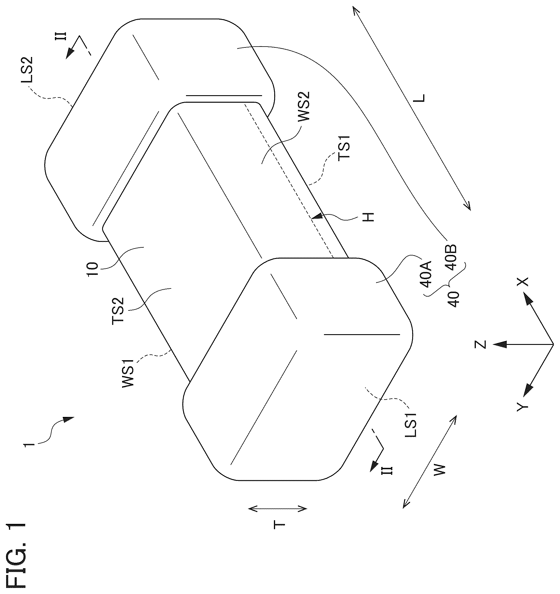
Hereinafter, a multilayer ceramic capacitor 1 according to a first preferred embodiment of the present disclosure will be described. is an external perspective view of the multilayer ceramic capacitor 1 according to the first preferred embodiment of the present invention. is a cross-sectional view taken along the line II-II of the multilayer ceramic capacitor 1 shown in . is a cross-sectional view taken along the line III-III of the multilayer ceramic capacitor 1 shown in . is a cross-sectional view taken along the line IV-IV of the multilayer ceramic capacitor 1 shown in .
The multilayer ceramic capacitor 1 includes a multilayer body 10 and external electrodes 40 .
The XYZ Cartesian coordinate system is shown in to 4 . The multilayer ceramic capacitor 1 and the multilayer body 10 each have a length direction L corresponding to the X direction. The multilayer ceramic capacitor 1 and the multilayer body 10 each have a width direction W corresponding to the Y direction. The multilayer ceramic capacitor 1 and the multilayer body 10 each have a lamination (stacking) direction T corresponding to the Z direction. Herein, the cross section shown in is also referred to as an LT cross section. The cross section shown in is also referred to as a WT cross section. The cross section shown in is also referred to as an LW cross section.
As shown in to 4 , the multilayer body 10 includes a first main surface TS 1 and a second main surface TS 2 which oppose each other in the lamination direction T, a first end surface LS 1 and a second end surface LS 2 which oppose each other in the length direction L perpendicular or substantially perpendicular to the lamination direction T, and a first side surface WS 1 and a second side surface WS 2 which oppose each other in the width direction W perpendicular or substantially perpendicular to the lamination direction T and the length direction L.
The multilayer body 10 has a rectangular or substantially rectangular parallelepiped shape. The dimension of the multilayer body 10 in the length direction L is not necessarily longer than the dimension of the width direction W. The multilayer body 10 preferably includes rounded corners and ridges. The corners are portions where the three surfaces of the multilayer body intersect, and the ridges are portions where the two surfaces of the multilayer body intersect. Unevenness or the like may be provided on a portion or the entirety of the surface of the multilayer body 10 .
The multilayer body 10 includes an inner layer portion 11 , and a first main surface-side outer layer portion 12 and a second main surface-side outer layer portion 13 which sandwich the inner layer portion 11 therebetween in the lamination direction T.
The inner layer portion 11 includes a plurality of dielectric layers 20 and a plurality of internal electrode layers 30 . The inner layer portion 11 includes, in the lamination direction T, internal electrode layers 30 from the internal electrode layer 30 located closest to the first main surface TS 1 to the internal electrode layer 30 located closest to the second main surface TS 2 . In the inner layer portion 11 , a plurality of internal electrode layers 30 oppose each other with the dielectric layer 20 interposed therebetween. The inner layer portion 11 generates a capacitance and substantially defines and functions as a capacitor. The inner layer portion 11 is also referred to as an effective layer portion.
The plurality of dielectric layers 20 are each made of a dielectric material. The dielectric material may be, for example, a dielectric ceramic including components such as a BaTiO 3 , CaTiO 3 , SrTiO 3 , or CaZrO 3 . Furthermore, the dielectric material may be obtained by adding a sub component such as a Mn compound, an Fe compound, a Cr compound, a Co compound, or a Ni compound to the main component.
The thickness of the dielectric layer 20 is preferably, for example, about 0.5 μm or more and about 10 μm or less. The number of the dielectric layers 20 to be laminated (stacked) is preferably 15 or more and 700 or less, for example. The number of the dielectric layers 20 refers to the total number of dielectric layers in the inner layer portion 11 , and dielectric layers in the first main surface-side outer layer portion 12 and the second main surface-side outer layer portion 13 .
The plurality of internal electrode layers 30 each include a plurality of first internal electrode layers 31 and a plurality of second internal electrode layers 32 . The plurality of first internal electrode layers 31 are each provided on the dielectric layer 20 . The plurality of second internal electrode layers 32 are each provided on the dielectric layer 20 . The plurality of first internal electrode layers 31 and the plurality of second internal electrode layers 32 are alternately provided via the dielectric layer 20 in the lamination direction T of the multilayer body 10 . The first internal electrode layers 31 and the second internal electrode layers 32 each sandwich the dielectric layers 20 .
The first internal electrode layer 31 includes a first opposing portion 31 A facing the second internal electrode layer 32 , and a first extension portion 31 B extending from the first opposing portion 31 A toward the first end surface LS 1 . The first extension portion 31 B is exposed on the first end surface LS 1 .
The second internal electrode layer 32 includes a second opposing portion 32 A facing the first internal electrode layer 31 , and a second extension portion 32 B extending from the second opposing portion 32 A toward the second end surface LS 2 . The second extension portion 32 B is exposed on the second end surface LS 2 .
In the present preferred embodiment, the first opposing portion 31 A and the second opposing portion 32 A are opposed to each other with the dielectric layers 20 interposed therebetween, such that a capacitance is generated, and the characteristics of a capacitor are provided.
The shapes of the first opposing portion 31 A and the second opposing portion 32 A are not particularly limited. However, for example, they are preferably rectangular or substantially rectangular. However, the corners of the rectangular or substantially rectangular shape may be rounded, or the corners of the rectangular or substantially rectangular shape may be slanted. The shapes of the first extension portion 31 B and the second extension portion 32 B are not particularly limited. However, for example, they are preferably rectangular or substantially rectangular. However, the corners of the rectangular or substantially rectangular shape may be rounded, or the corners of the rectangular or substantially rectangular shape may be slanted.
The dimension in the width direction W of the first opposing portion 31 A may be the same or substantially same as the dimension in the width direction W of the first extension portion 31 B, or either of them may be smaller. The dimension in the width direction W of the second opposing portion 32 A may be the same or substantially the same as the dimension in the width direction W of the second extension portion 32 B, or either of them may be smaller.
The first internal electrode layer 31 and the second internal electrode layer 32 are each made of an appropriate conductive material including, for example, a metal such as Ni, Cu, Ag, Pd, and Au, and an alloy including at least one of these metals. When using an alloy, the first internal electrode layer 31 and the second internal electrode layer 32 may be made of a Ag—Pd alloy or the like, for example.
The thickness of each of the first internal electrode layers 31 and the second internal electrode layers 32 is preferably, for example, about 0.2 μm or more and about 2.0 μm or less. The total number of the first internal electrode layers 31 and the second internal electrode layers 32 is preferably 15 or more and 200 or less, for example.
The first main surface-side outer layer portion 12 is located in the vicinity of the first main surface TS 1 of the multilayer body 10 . The first main surface-side outer layer portion 12 includes a plurality of dielectric layers 20 located between the first main surface TS 1 and the internal electrode layer 30 closest to the first main surface TS 1 . That is, the first main surface-side outer layer portion 12 includes a plurality of dielectric layers 20 . The plurality of dielectric layers 20 are provided between the first main surface TS 1 and the internal electrode layer 30 located closest to the first main surface TS 1 among the plurality of internal electrode layers 30 . The dielectric layers 20 used in the first main surface-side outer layer portion 12 may be the same as the dielectric layers 20 used in the inner layer portion 11 .
The second main surface-side outer layer portion 13 is located in the vicinity of the second main surface TS 2 of the multilayer body 10 . The second main surface-side outer layer portion 13 includes a plurality of dielectric layers 20 located between the second main surface TS 2 and the internal electrode layer 30 closest to the second main surface TS 2 . That is, the second main surface-side outer layer portion 13 includes a plurality of dielectric layers 20 . The plurality of dielectric layers 20 are provided between the second main surface TS 2 and the internal electrode layer 30 closest to the second main surface TS 2 among the plurality of internal electrode layers 30 . The dielectric layers 20 used in the second main surface-side outer layer portion 13 may be the same as the dielectric layers 20 used in the inner layer portion 11 .
As described above, the multilayer body 10 includes a plurality of stacked dielectric layers 20 , and a plurality of stacked internal electrode layers 30 on the dielectric layer 20 . That is, the multilayer ceramic capacitor 1 includes the multilayer body 10 . In the multilayer body 10 , the dielectric layer 20 and the internal electrode layer 30 are alternately laminated.
The multilayer body 10 includes a counter electrode portion 11 E. The counter electrode portion 11 E refers to a portion where the first opposing portion 31 A of the first internal electrode layer 31 and the second opposing portion 32 A of the second internal electrode layer 32 oppose each other. The counter electrode portion 11 E defines and functions as a portion of the inner layer portion 11 . shows the range of the counter electrode portion 11 E in the width direction W and in the length direction L. The counter electrode portion 11 E is also referred to as a capacitor active portion.
The multilayer body 10 includes end surface-side outer layer portions. The end surface-side outer layer portions include a first end surface-side outer layer portion LG 1 and a second end surface-side outer layer portion LG 2 . The first end surface-side outer layer portion LG 1 includes the dielectric layer 20 and the first extension portion 31 B located between the counter electrode portion 11 E and the first end surface LS 1 . The second end surface-side outer layer portion LG 2 includes the dielectric layer 20 and the second extension portion 32 B located between the counter electrode portion 11 E and the second end surface LS 2 . each show the ranges in the length direction L of the first end surface-side outer layer portion LG 1 and the second end surface-side outer layer portion LG 2 . The first end surface-side outer layer portion LG 1 and the second end surface-side outer layer portion LG 2 may also be referred to as L gaps or end gaps.
The multilayer body 10 includes side surface-side outer layer portions. Furthermore, the side surface-side outer layer portion includes a first side surface-side outer layer portion WG 1 and a second side surface-side outer layer portion WG 2 . The first side surface-side outer layer portion WG 1 includes a dielectric layer 20 located between the counter electrode portion 11 E and the first side surface WS 1 . The second side surface-side outer layer portion WG 2 includes the dielectric layers 20 located between the counter electrode portion 11 E and the second side surface WS 2 . shows the ranges of the first side surface-side outer layer portion WG 1 and the second side surface-side outer layer portion WG 2 in the width direction W. The first side surface-side outer layer portion WG 1 and the second side surface-side outer layer portion WG 2 may also be referred to as W gaps or side gaps.
The external electrode 40 includes a first external electrode 40 A provided in the vicinity of the first end surface LS 1 , and a second external electrode 40 B provided in the vicinity of the second end surface LS 2 .
The first external electrode 40 A is provided on the first end surface LS 1 . The first external electrode 40 A is connected to the first internal electrode layer 31 . The first external electrode 40 A may be provided on a portion of the first main surface TS 1 and a portion of the second main surface TS 2 , and a portion of the first side surface WS 1 and a portion of the second side surface WS 2 . In the present preferred embodiment, the first external electrode 40 A extends from the first end surface LS 1 to a portion of the first main surface TS 1 , a portion of the second main surface TS 2 , a portion of the first side surface WS 1 , and a portion of the second side surface WS 2 .
The second external electrode 40 B is provided on the second end surface LS 2 . The second external electrode 40 B is connected to the second internal electrode layer 32 . The second external electrode 40 B may be provided on a portion of the first main surface TS 1 and a portion of the second main surface TS 2 , and a portion of the first side surface WS 1 and a portion of the second side surface WS 2 . In the present preferred embodiment, the second external electrode 40 B extends from the second end surface LS 2 to a portion of the first main surface TS 1 , a portion of the second main surface TS 2 , a portion of the first side surface WS 1 , and a portion of the second side surface WS 2 .
As described above, in the multilayer body 10 , the capacitance is generated by the first opposing portions 31 A of the first internal electrode layers 31 and the second opposing portions 32 A of the second internal electrode layers 32 opposing each other with the dielectric layers 20 interposed therebetween. Therefore, characteristics of the capacitor are developed between the first external electrode 40 A to which the first internal electrode layers 31 are connected and the second external electrode 40 B to which the second internal electrode layers 32 are connected.
The first external electrode 40 A includes a first base electrode layer 50 A and a first plated layer 60 A provided on the first base electrode layer 50 A.
The second external electrode 40 B includes a second base electrode layer 50 B and a second plated layer 60 B provided on the second base electrode layer 50 B.
The first base electrode layer 50 A is provided on the first end surface LS 1 . The first base electrode layer 50 A is connected to the first internal electrode layer 31 . In the present preferred embodiment of the present invention, the first base electrode layer 50 A extends from the first end surface LS 1 to a portion of the first main surface TS 1 , a portion of the second main surface TS 2 , a portion of the first side surface WS 1 , and a portion of the second side surface WS 2 . The first base electrode layer 50 A may be provided only on the surface of the first end surface LS 1 of the multilayer body.
The second base electrode layer 50 B is provided on the second end surface LS 2 . The second base electrode layer 50 B is connected to the second internal electrode layer 32 . In the present preferred embodiment of the present invention, the second base electrode layer 50 B extends from the second end surface LS 2 to a portion of the first main surface TS 1 , a portion of the second main surface TS 2 , a portion of the first side surface WS 1 , and a portion of the second side surface WS 2 . The second base electrode layer 50 B may be provided only on the surface of the second end surface LS 2 of the multilayer body.
The first base electrode layer 50 A and the second base electrode layer 50 B include at least one layer selected from a fired layer, a thin film layer, or other layers. The first base electrode layer 50 A and the second base electrode layer 50 B may be hereinafter collectively referred to as a base electrode layer.
The base electrode layer of the present preferred embodiment of the present invention is a fired layer, for example. The fired layer preferably includes a metal component and a ceramic component. As a result, the adhesion between the multilayer body 10 and the base electrode layer can be improved. As the metal component included in the fired layer, at least one selected from metals such as, for example, Ni, Cu, Ag, Pd, Au, Ag—Pd alloy is used. Among them, Ni is preferably used. For example, in a case where the internal electrode layer 30 is made of Ni, if the metal of the base electrode layer is Ni which is the same type of metal, the metal bonding strength increases. Therefore, the continuity of the joint between the internal electrode layer 30 and the base electrode layer increases. As a result, a discharge efficiency for discharging hydrogen occluded to the internal electrode layer 30 can be improved, which will be described later.
For the ceramic component, a ceramic material of the same kind as that of the dielectric layer 20 may be used, or a ceramic material of a different kind may be used. The ceramic component includes, for example, at least one selected from BaTiO 3 , CaTiO 3 , (Ba, Ca) TiO 3 , SrTiO 3 , CaZrO 3 , or the like.
The fired layer is preferably a laminate chip including internal electrode layers and dielectric layers and a conductive paste applied to the laminate chip simultaneously fired. In this case, a ceramic material of the same kind as that of the dielectric layer 20 is particularly preferably used. Thus, it is preferable that the base electrode layer includes a metal component and a dielectric material.
Furthermore, the fired layer is preferably a laminate chip including internal electrode layers and dielectric layers fired to obtain the multilayer body, following which a conductive paste may be applied to the multilayer body and fired. Furthermore, the fired layer may include a metal component and a glass component.
Furthermore, the base electrode layer may include a plurality of base electrode layers.
The thickness in the length direction of the first base electrode layer 50 A provided on the first end surface LS 1 is preferably, for example, about 1 μm or more and about 160 μm or less in the middle portion in the height (lamination) direction T and the width direction W of the first base electrode layer 50 A.
The thickness in the length direction of the second base electrode layer 50 B provided on the second end surface LS 2 is preferably, for example, about 1 μm or more and about 160 μm or less at the middle portion in the height direction T and the width direction W of the second base electrode layer 50 B.
When the first base electrode layer 50 A is provided on a portion of at least one surface of the first main surface TS 1 and the second main surface TS 2 , the thickness of the first base electrode layer 50 A provided in this portion in the height direction is preferably, for example, about 1 μm or more and about 40 μm or less at the middle portion in the length direction L and the width direction W of the first base electrode layer 50 A provided in this portion.
The first base electrode layer 50 A may be provided on a portion of at least one surface of the first side surface WS 1 and the second side surface WS 2 . In this case, the thickness of the first base electrode layer 50 A provided in this portion in the width direction is preferably, for example, about 1 μm or more and about 40 μm or less at the middle portion in the length direction L and the height direction T of the first base electrode layer 50 A provided in this portion.
The second base electrode layer 50 B may be provided on a portion of at least one surface of the first main surface TS 1 and the second main surface TS 2 . In this case, the thickness of the second base electrode layer 50 B provided in this portion in the height direction is preferably, for example, about 1 μm or more and about 40 μm or less at the middle portion in the length direction L and the width direction W of the second base electrode layer 50 B provided in this portion.
The second base electrode layer 50 B may be provided on a portion of at least one surface of the first side surface WS 1 and the second side surface WS 2 . In this case, the thickness of the second base electrode layer 50 B provided in this portion in the width direction is preferably, for example, about 1 μm or more and 40 μm or less at the middle portion in the length direction L and the height direction T of the second base electrode layer 50 B provided in this portion.
The first plated layer 60 A covers the first base electrode layer 50 A.
The second plated layer 60 B covers the second base electrode layer 50 B.
The first plated layer 60 A and the second plated layer 60 B may include at least one selected from, for example, Cu, Ni, Sn, Ag, Pd, Ag—Pd alloys, Au, or the like. Hereinafter, the first plated layer 60 A and the second plated layer 60 B are also collectively referred to as a plated layer. More preferably, the plated layer includes, for example, at least one of Cu, Ni, and Sn. Alternatively, the plated layer includes, for example, two or more of Cu, Ni, and Sn.
Each of the first plated layer 60 A and the second plated layer 60 B may include a plurality of layers.
For example, the plated layer may include a two-layer structure. In the two-layer structure, the Sn plated layer may be provided on the Ni plated layer.
For example, as shown in to 4 , the first plated layer 60 A may include a first Ni plated layer 61 A and a first Sn plated layer 62 A. The first Ni plated layer 61 A may be provided on the first base electrode layer 50 A. The first Sn plated layer 62 A may be provided on the first Ni plated layer 61 A.
The second plated layer 60 B may include a second Ni plated layer 61 B and a second Sn plated layer 62 B. The second Ni plated layer 61 B is provided on the second base electrode layer 50 B. The second Sn plated layer 62 B is provided on the second Ni plated layer 61 B.
The Ni plated layer reduces or prevents the erosion of the base electrode layer by solder at the time of mounting the multilayer ceramic capacitor 1 . Furthermore, the Sn plated layer improves the wettability of solder when mounting the multilayer ceramic capacitor 1 . Thus, it is possible to easily mount the multilayer ceramic capacitor 1 .
Furthermore, the configuration of the two plated layers including only the Ni plated layer and the Sn plated layer without a Cu plated layer to be described later makes it possible to provide a thinner external electrode 40 . Therefore, the degree of freedom in design of the dimensions of the multilayer body 10 is improved, and thus it is possible to contribute to capacitance expansion. Even when a Cu plated layer is not provided, it is still possible to ensure moisture resistance by the base electrode layer.
The plated layer is not limited to the two-layer structure. The plated layer preferably includes, for example, a three-layer structure including a Cu plated layer, a Ni plated layer, and a Sn plated layer. A is a LT cross-sectional view showing a multilayer ceramic capacitor 1 when a plated layer has a three-layer structure, and corresponding to .
For example, as shown in A , the first plated layer 60 A preferably includes a first Cu plated layer 63 A, a first Ni plated layer 61 A, and a first Sn plated layer 62 A. The first Cu plated layer 63 A is provided on the first base electrode layer 50 A. The first Ni plated layer 61 A is provided on the first Cu plated layer 63 A. The first Sn plated layer 62 A is provided on the first Ni plated layer 61 A.
The second plated layer 60 B preferably includes a second Cu plated layer 63 B, a second Ni plated layer 61 B, and a second Sn plated layer 62 B. The second Cu plated layer 63 B is provided on the second base electrode layer 50 B. The second Ni plated layer 61 B is provided on the second Cu plated layer 63 B. The second Sn plated layer 62 B is provided on the second Ni plated layer 61 B.
The Cu plated layer has high moisture resistance. Therefore, by providing the Cu plated layer, it is possible to further reduce or prevent moisture from entering the inside of the external electrode 40 from the outside.
The plated layer may be made solely from a Sn plated layer. B is an LT cross-sectional view showing a multilayer ceramic capacitor 1 when a plated layer includes solely a Sn plated layer, and corresponding to .
For example, as shown in B , the first plated layer 60 A may include the first Sn plated layer 62 A. The first Sn plated layer 62 A is provided on the first base electrode layer 50 A.
The second plated layer 60 B may include the second Sn plated layer 62 B. The second Sn plated layer 62 B is provided on the second base electrode layer 50 B.
The configuration of the plated layer including only the Sn plated layer without the Cu plated layer and the Ni plated layer makes it possible to provide a thinner external electrode 40 . Therefore, the degree of freedom in design of the dimensions of the multilayer body 10 is improved, and thus it is possible to contribute to capacitance expansion. In this case, Ni may be used as a metal of the base electrode layer. Thus, with only the base electrode layer, it is possible to reduce or prevent the erosion of the external electrode by solder when mounting the multilayer ceramic capacitor 1 .
The plated layer may be directly provided on the first end surface LS 1 and the second end surface LS 2 . C is an LT cross-sectional view showing a multilayer ceramic capacitor 1 in which the plated layer is provided directly on the first end surface LS 1 and the second end surface LS 2 , and corresponding to .
In the example illustrated in C , the first base electrode layer 50 A is not provided on the first end surface LS 1 of the multilayer body. The first base electrode layer 50 A is provided on a portion of the first main surface TS 1 and a portion of the second main surface TS 2 in the vicinity of the first end surface LS 1 . Although not shown, the first base electrode layer 50 A is provided on a portion of the first side surface WS 1 and a portion of the second side surface WS 2 in the vicinity of the first end surface LS 1 .
The first plated layer 60 A is provided directly on the multilayer body 10 on the first end surface LS 1 . On the first main surface TS 1 , the second main surface TS 2 , the first side surface WS 1 , and the second side surface WS 2 , the first plated layer 60 A covers the first base electrode layer 50 A provided on the first main surface TS 1 , the second main surface TS 2 , the first side surface WS 1 , and the second side surface WS 2 . Thus, the first plated layer 60 A is provided on the first end surface LS 1 without the base electrode layer interposed therebetween.
In the example shown in C , the second base electrode layer 50 B is not provided on the second end surface LS 2 . The second base electrode layer 50 B is provided on a portion of the first main surface TS 1 and a portion of the second main surface TS 2 in the vicinity of the second end surface LS 2 . Although not shown, the second base electrode layer 50 B is provided on a portion of the first side surface WS 1 and a portion of the second side surface WS 2 in the vicinity of the second end surface LS 2 .
The second plated layer 60 B is provided directly on the multilayer body 10 on the second end surface LS 2 . On the first main surface TS 1 , the second main surface TS 2 , the first side surface WS 1 , and the second side surface WS 2 , the second plated layer 60 B covers the second base electrode layer 50 B provided on the first main surface TS 1 , the second main surface TS 2 , the first side surface WS 1 , and the second side surface WS 2 . Thus, the second plated layer 60 B is provided on the second end surface LS 2 without the base electrode layer interposed therebetween.
In this case, it is preferable that the first plated layer 60 A and the second plated layer 60 B each include a plurality of layers.
For example, as shown in C , the first plated layer 60 A preferably includes the first Ni plated layer 61 A and the first Sn plated layer 62 A. The first Ni plated layer 61 A is provided on the first end surface LS 1 . The first Sn plated layer 62 A is provided on the first Ni plated layer 61 A.
For example, as shown in C , the second plated layer 60 B preferably includes the second Ni plated layer 61 B and the second Sn plated layer 62 B. The second Ni plated layer 61 B is provided on the second end surface LS 2 . The second Sn plated layer 62 B is provided on the second Ni plated layer 61 B.
More specifically, the first Ni plated layer 61 A is provided directly on the multilayer body 10 , on the first end surface LS 1 . On the first main surface TS 1 , the second main surface TS 2 , the first side surface WS 1 , and the second side surface WS 2 , the first Ni plated layer 61 A covers the first base electrode layer 50 A provided on the first main surface TS 1 , the second main surface TS 2 , the first side surface WS 1 , and the second side surface WS 2 . The first Sn plated layer 62 A covers the first Ni plated layer 61 A.
The second Ni plated layer 61 B is provided directly on the multilayer body 10 , on the second end surface LS 2 . On the first main surface TS 1 , the second main surface TS 2 , the first side surface WS 1 , and the second side surface WS 2 , the second Ni plated layer 61 B covers the second base electrode layer 50 B provided on the first main surface TS 1 , the second main surface TS 2 , the first side surface WS 1 , and the second side surface WS 2 . The second Sn plated layer 62 B covers the second Ni plated layer 61 B.
Thus, by using Ni as a metal of the plated layer provided directly on the multilayer body 10 , even without providing the base electrode layer, it is possible to reduce or prevent the erosion of the external electrode by solder at the time of mounting the multilayer ceramic capacitor 1 . Furthermore, providing the Sn plated layer improves the wettability of the solder when mounting the multilayer ceramic capacitor 1 . This facilitates the mounting of the multilayer ceramic capacitor 1 .
Furthermore, since the first end surface and the second end surface are not provided with a base electrode layer, it is possible to provide a thinner external electrode 40 . Therefore, the degree of freedom in design of the dimensions of the multilayer body 10 is improved, and thus it is possible to contribute to capacitance expansion.
The external electrode 40 may include only the plated layer without the base electrode layer.
The thickness per layer of the plated layer including the first plated layer 60 A and the second plated layer 60 B is preferably about 1 μm or more and about 15 μm or less, for example. That is, for example, the thickness of each of the first Cu plated layer 63 A, the first Ni plated layer 61 A, the first Sn plated layer 62 A, the second Cu plated layer 63 B, the second Ni plated layer 61 B, and the second Sn plated layer 62 B as described above is preferably about 1 μm or more and about 15 μm or less.
As in the various examples described above, the external electrode 40 preferably includes an inner layer including Ni as a metal component and an outer layer including Sn as a metal component. The outer layer is provided on the outer surface-side of the inner layer. The inner layer including Ni as a metal component is preferably provided on the surface of the multilayer body 10 where the internal electrode layers 30 are exposed. The outer layer including Sn as a metal component preferably covers the inner layer. For example, the first external electrode 40 A may include a first inner layer including Ni as a metal component and a first outer layer including Sn as a metal component. The first inner layer may be provided on the first end surface LS 1 . The first outer layer may be provided on an outer surface-side of the first inner layer. The second external electrode 40 B may include a second inner layer including Ni as a metal component and a second outer layer including Sn as a metal component. The second inner layer may be provided on the second end surface LS 2 . The second outer layer may be provided on the outer surface-side of the second inner layer. As the external electrode 40 including Ni as a main component of the metal component, for example, a fired layer including Ni may be used, or a Ni plated layer may be used. As the outer layer including Sn as a main component of the metal component, for example, a Sn plated layer may be used.
When the dimension in the length direction of the multilayer ceramic capacitor 1 including the multilayer body 10 and the external electrode 40 is defined as the L dimension, the L dimension is preferably about 0.02 mm or more and about 2.1 mm or less, for example. Furthermore, when the dimension in the height direction of the multilayer ceramic capacitor 1 is defined as the T dimension, the T dimension is preferably about 0.01 mm or more and about 1.8 mm or less, for example. Furthermore, when the dimension in the width direction of the multilayer ceramic capacitor 1 is defined as the W dimension, the W dimension is preferably about 0.01 mm or more and about 1.8 mm or less, for example.
The multilayer ceramic capacitor 1 of the present preferred embodiment includes a discharge path P. The discharge path P can discharge a chemical element to the outside of the multilayer body 10 .
The discharge path P is provided in at least one of the first main surface-side outer layer portion 12 and the second main surface-side outer layer portion 13 of the multilayer body 10 . In the present preferred embodiment, the discharge path P is provided in the first main surface-side outer layer portion 12 . The discharge path P is provided along the LW cross-section, i.e., a plane perpendicular or substantially perpendicular to the stacking (lamination) direction T. In other words, the discharge path P is provided along a plane extending in the length direction L and the width direction W.
is an enlarged view of the VI portion in , and is an enlarged cross-sectional view schematically showing a cross section of the discharge path P.
As shown in , the discharge path P includes a plurality of cavities 80 . The plurality of cavities 80 are provided in a plane perpendicular or substantially perpendicular to the stacking direction T. The cavities 80 may each include a spherically curved surface. The plurality of cavities 80 are coupled together to provide the discharge path P.
The discharge path P is, for example, provided between the plurality of dielectric layers 20 including the first main surface-side outer layer portion 12 . illustrates an example where the discharge path P is provided at a boundary surface BS between the first dielectric layer 20 A and the second dielectric layer 20 B. The first dielectric layer 20 A and the second dielectric layer 20 B are included in the plurality of dielectric layers 20 including the first main surface-side outer layer portion 12 . The second dielectric layer 20 B is overlaid with the first dielectric layer 20 A.
More specifically, a plurality of recesses are provided in the surface of the first dielectric layer 20 A which opposes the second dielectric layer 20 B. Furthermore, a plurality of recesses are provided in the surface of the second dielectric layer 20 B which opposes the first dielectric layer 20 A. The surfaces each including the plurality of recesses are opposed to each other. With such a configuration, the plurality of recesses provide the plurality of cavities 80 . Furthermore, the plurality of recesses provided in the first dielectric layer 20 A, and the plurality of recesses provided in the second dielectric layer 20 B are provided at positions shifted from each other in a direction perpendicular or substantially perpendicular to the stacking direction T. For example, shows an example in which the plurality of recesses provided in the first dielectric layer 20 A, and the plurality of recesses provided in the second dielectric layer 20 B are provided at positions shifted from each other in the length direction L. With such a configuration, the plurality of cavities 80 is connected to each other to provide the discharge path P.
is an LW cross-sectional view taken along the line VII-VII of the multilayer ceramic capacitor 1 shown in , and is a cross-sectional view taken along a plane along the boundary surface BS between the first dielectric layer 20 A and the second dielectric layer 20 B, i.e., a plane where the discharge path P is provided. In other words, is a diagram of a surface of the first dielectric layer 20 A facing the second dielectric layer 20 B among the plurality of dielectric layers 20 included in the first main surface-side outer layer portion 12 .
A is an enlarged view of the VIIIA portion in , and is an enlarged view schematically showing a microscopic state in a plane view of the surface of the first dielectric layer 20 A. B is an enlarged cross-sectional view schematically showing a cross-section near the surface of the first dielectric layer 20 A along the line VIIIB-VIIIB of the surface of A . In B , only the first dielectric layer 20 A is shown, and the second dielectric layer 20 B is not shown.
As shown in A and 8 B , the plurality of recesses each including a spherical curved surface is provided on the surface of the first dielectric layer 20 A. Here, the plurality of recesses are portions that provide the cavities 80 in . For this reason, like the cavities 80 , the plurality of recesses is each denoted by the reference numeral 80 .
The plurality of recesses 80 are provided on the surface of the first dielectric layer 20 A. In the present preferred embodiment, the plurality of recesses 80 having the same size or substantially the same size are provided in a plane.
As shown in A , the plurality of recesses 80 may be provided, for example, in a hexagonal close-packed shape on the surface of the first dielectric layer 20 A. By providing the plurality of recesses 80 in such a hexagonal close-packed shape, it is possible to provide the plurality of recesses 80 on the surface of the first dielectric layer 20 A at a high density. For example, the plurality of recesses 80 may be provided such that an average of 5 or more and 7 or less other recesses 80 are located around a single recess 80 . Thus, it is possible to provide the plurality of recesses 80 on the surface of the first dielectric layer 20 A at a high density. By providing the recesses 80 at a high density in this manner, the discharge path P can be easily provided. In addition, the fluid can easily pass through the discharge path P. The plurality of recesses 80 may be regularly arranged. However, the plurality of recesses 80 may not be regularly arranged.
Each of the plurality of recesses 80 includes an opening 81 and a wall 82 . As shown in A , in the present preferred embodiment of the present invention, the opening 81 includes an outer edge portion of the recess 80 . The opening 81 has a circular or substantially circular shape, for example.
As shown in B , the wall 82 of the recess 80 includes a spherical curved surface in the cross section. That is, the wall 82 of the recess 80 includes a concave curved surface. The concave curved surface may be a portion of the surface of the sphere. The wall surface of the recess 80 may have a hemispherical shape. However, the wall surface 82 of the recess 80 may have a spherical curved surface less than a hemisphere.
The surface of the first dielectric layer 20 A includes the plurality of recesses 80 and a plurality of land portions 90 . The plurality of recesses 80 each include a spherical curved surface. The plurality of land portions 90 are regions in which the plurality of recesses 80 are not provided.
The average inlet size of the plurality of recesses 80 provided on the surface of the first dielectric layers 20 A is preferably about 0.2 μm or more and about 2 μm or less, for example. The average depth of the plurality of recesses 80 provided on the surface of the first dielectric layers 20 A is preferably about 0.1 μm or more and about 1 μm or less, for example.
Here, the depth of the recess 80 is defined as the maximum value of the distance in the depth direction of the recess 80 from the deepest portion of the recess 80 to the opening 81 of the recess 80 .
The average depth of the plurality of recesses 80 provided on the surface of the first dielectric layer 20 A may be, for example, about 25% or more and about 50% or less of the plurality of recesses 80 of the average inlet size.
The plurality of recesses 80 are also similarly provided on the surface of the second dielectric layer 20 B facing the first dielectric layer 20 A. Thus, the surfaces each including the plurality of recesses 80 are opposed to each other. This provides the plurality of cavities 80 and the discharge path P. Here, the cavities 80 providing the discharge path P each include a spherical curved surface. As a result, the resistance when the fluid passes through the discharge path P is reduced.
Here, the height in the stacking direction T of the cavity 80 is the same as or similar to the depth of the recess 80 . Therefore, it is preferable that the average height of the plurality of cavities 80 in the stacking direction T is about 0.1 μm or more and about 1 μm or less, for example. As a result, the discharge path P can be easily provided.
The shape of the cavities 80 providing the discharge path P is not particularly limited. However, the cavities 80 are each preferably provided such that dielectric pillars 91 remain. Here, the dielectric pillars 91 are each provided by a solid portion of the dielectric material located between the plurality of cavities 80 . That is, the solid portion located between the plurality of recesses 80 shown in provides the dielectric pillars 91 .
Here, at the boundary surface BS of the plurality of dielectric layers 20 , there are portions where the opposing cavities 80 are connected to each other and portions where the opposing land portions 90 are in contact with each other. Thus, the land portions 90 of the surface of the dielectric layer 20 is in contact with the land portions 90 of the surface of the opposing dielectric layer 20 . This provides the solid portion of the dielectric material located between the plurality of cavities 80 . As a result, the dielectric pillar 91 is provided.
The plurality of cavities 80 are coupled together to provide the discharge path P. When viewed in a three-dimensional manner, a portion of one cavity 80 is coupled to a portion of another cavity 80 . Such a connection state between the plurality of cavities is consecutive, thus providing the path P through which a chemical element can be discharged. In addition, in the plane in which the cavities 80 are provided, it is only necessary to provide the discharge path P in which a chemical element can be discharged by continuing the connection state between the plurality of cavities in any of the paths. Thus, some cavities may be isolated from the plurality of cavities 80 .
With such a configuration, it is possible to establish a portion, where the first main surface-side outer layer portion 12 closer to the first main surface TS 1 than the location where the cavities 80 are provided, is in contact with the first main surface-side outer layer portion 12 closer to the second main surface TS 2 than the location where the cavities 80 are provided. Therefore, it is possible to improve the adhesion between the first main surface-side outer layer portion 12 closer to the first main surface TS 1 than the location where the cavities 80 are provided, and the first main surface-side outer layer portion 12 closer to the second main surface TS 2 than the location where the cavities 80 are provided. That is, it is possible to improve the adhesion between the first dielectric layer 20 A and the second dielectric layer 20 B between which the discharge path P is provided. As a result, the discharge path P can be provided in the first main surface-side outer layer portion 12 while maintaining the connectivity of the first main surface-side outer layer portion 12 itself.
With the above configuration, the plurality of cavities 80 can be easily connected to each other. Furthermore, it is possible to provide the continuous cavities 80 . The continuous cavities 80 allow a chemical element to be discharged out of the multilayer body 10 within the range from the first end surface LS 1 to the second end surface LS 2 , on the same plane. Therefore, even when hydrogen is occluded in the internal electrode layer 30 , the hydrogen occluded in the internal electrode layer 30 is easily discharged from the external electrode 40 to the outside of the multilayer ceramic capacitor 1 through the cavities 80 .
The plurality of recesses 80 provided on the surfaces of the dielectric layers 20 A and 20 B opposing each other are not limited to those shown in A and B . For example, the plurality of recesses 80 may be those as shown in A and 9 B . A and 9 B are diagrams of other examples of the plurality of recesses 80 . A corresponds to A . B corresponds to B .
As shown in A and 9 B , the plurality of recesses 80 may include recesses of differing inlet sizes. For example, as shown in A and 9 B , the plurality of recesses 80 may include recesses 80 B and recesses 80 C. The recesses 80 B each have a larger inlet size relative to the average inlet size. The recesses 80 C each have a smaller inlet size relative to the average inlet size. In this case, the average depth of the recesses 80 C each having an inlet size smaller than the average inlet size may be smaller than the average depth of the recesses 80 B, each having a larger inlet size with respect to the average inlet size. The recesses 80 B each having a larger inlet size with respect to the average inlet size, and the recesses 80 C each having a smaller inlet size with respect to the average inlet size may be regularly arranged. Alternatively, they may not be regularly arranged. Furthermore, the plurality of recesses 80 may include a plurality of recesses in which the inlet sizes differ in a stepwise manner or randomly.
The plurality of recesses 80 B and 80 C of different inlet sizes each include, for example, circular or substantially circular openings 81 B and 81 C, and walls 82 B and 82 C each including a spherical curved surface. The openings 81 B and 81 C are not limited to being circular or substantially circular, and may have other shapes. The wall 82 B of the recess 80 B may include a hemispherical or substantially hemispherical shape, or a spherical curved surface less than a hemisphere, for example. Furthermore, the wall 82 C of the recess 80 C may include a spherical curved surface less than the hemisphere.
Also in this case, it is preferable that the average inlet size of the plurality of recesses 80 is about 0.2 μm or more and about 2 μm or less, for example. The average depth of the plurality of recesses 80 is preferably about 0.1 μm or more and about 1 μm or less, for example.
The plurality of recesses 80 provided on the surfaces of the dielectric layers 20 A and 20 B opposing each other may include a configuration shown in A and 10 B . A and 10 B are diagrams of other examples of the plurality of recesses 80 . A corresponds to A . B corresponds to B .
As shown in A and 10 B , the plurality of recesses 80 may include recesses 80 D. The recesses 80 D each include an opening 81 D having a hexagonal or substantially hexagonal shape. This makes it possible to provide the plurality of recesses 80 at a higher density.
Also in this case, the wall surface 82 D of the recess 80 D may include a spherical curved surface. That is, the wall surface 82 D of the recess 80 D may include a concave curved surface including a portion of the surface of the sphere.
Also in this case, it is preferable that the average inlet size of the plurality of recesses 80 is about 0.2 μm or more and about 2 μm or less, for example. The average depth of the plurality of recesses 80 is preferably about 0.1 μm or more and about 1 μm or less, for example.
The recesses of different inlet sizes and different shapes of openings as shown in A and 8 B , A and 9 B , and A and 10 B may coexist. Furthermore, the average inlet size of the plurality of recesses 80 provided on the surface of the first dielectric layer 20 A, and the average inlet size of the plurality of recesses 80 provided on the surface of the second dielectric layer 20 B may differ.
The discharge path P includes a path connecting between an opening H provided on the surface of the multilayer body 10 which is exposed from the external electrode 40 and the first end surface LS 1 on which the first external electrode 40 A is provided, and a path connecting between the opening H provided on the surface of the multilayer body 10 which is exposed from the external electrode 40 and the second end surface LS 2 on which the second external electrode 40 B is provided. The opening H is preferably provided on at least one of the first side surface WS 1 or the second side surface WS 2 , for example. In the present preferred embodiment of the present invention, the openings H are provided on the first side surface WS 1 and the second side surface WS 2 .
shows the region of the opening H provided in the second side surface WS 2 . The opening H is provided in the surface of the multilayer body 10 exposed from the first external electrode 40 A and the second external electrode 40 B. That is, the opening H is provided in the exposed surface of the multilayer body 10 . In the present preferred embodiment of the present invention, the opening H is provided at the same or substantially the same location in the stacking direction T as the plane in which the discharge path P is provided, on the first side surface WS 1 and the second side surface WS 2 . In the present preferred embodiment of the present invention, the opening H is provided as a continuous portion from the planar discharge path P. Therefore, the opening H has a shape the same as or similar to the cross section of the discharge path P shown in .
In the present preferred embodiment of the present invention, the plurality of cavities 80 providing the discharge path P is provided over the entire or substantially the entire surface of the dielectric layer 20 , i.e., on the entire or substantially the entire surface of the plane perpendicular or substantially perpendicular to the stacking direction T, between the plurality of dielectric layers 20 including the first main surface-side outer layer portion 12 . More specifically, as shown in , the recesses 80 providing the discharge path P are provided over the entire or substantially the entire surface of the first dielectric layer 20 A. That is, the discharge path P is substantially provided on the entire or substantially the entire surface of the plane perpendicular or substantially perpendicular to the stacking direction T of the first dielectric layer 20 A.
Thus, the plurality of cavities 80 are preferably provided over the entire or substantially the entire surface of the dielectric layer 20 that provides at least one of the first main surface-side outer layer portion 12 or the second main surface-side outer layer portion 13 . As a result, the total area of the path through which the fluid passes can be increased.
With the above configuration, the path connecting between the opening H provided on the surface of the multilayer body 10 which is exposed from the external electrode 40 , and the first end surface LS 1 where the first external electrode 40 A is provided, and the path connecting between the opening H provided on the surface of the multilayer body 10 which is exposed from the external electrode 40 , and the second end surface LS 2 where the second external electrode 40 B is provided, are provided as the discharge path P.
Thus, the plurality of cavities 80 preferably have a continuous path from at least the first end surface LS 1 and the second end surface LS 2 to the first side surface WS 1 or the second side surface WS 2 of the multilayer body 10 . That is, preferably, the plurality of cavities 80 are provided on the same plane from the first end surface LS 1 to the second end surface LS 2 . The plurality of cavities 80 can discharge a chemical element to the outside of the multilayer body 10 .
In the present preferred embodiment of the present invention, the discharge path P is provided as a path connecting the surface of the multilayer body 10 covered by the external electrode 40 and the surface of the multilayer body 10 exposed from the external electrode 40 . With such a configuration, even when hydrogen is occluded in the internal electrode layer 30 , the hydrogen occluded in the internal electrode layer 30 can be discharged to the outside of the multilayer ceramic capacitor 1 through the external electrode 40 and the discharge path P. Furthermore, even when the hydrogen is occluded in the external electrode 40 , it is possible to discharge the hydrogen occluded in the external electrode 40 to the outside of the multilayer ceramic capacitor 1 . Therefore, the amount of hydrogen included in the internal electrode layer 30 can be reduced, and the diffusion of hydrogen into the dielectric layer 20 can be reduced. As a result, it is possible to reduce or prevent the deterioration of the insulation resistance of the multilayer ceramic capacitor 1 .
Conventionally, multilayer ceramic capacitors including a multilayer body and a pair of external electrodes are known. In the multilayer body, a plurality of dielectric layers and a plurality of internal electrodes are laminated alternately. The pair of external electrodes are provided on the surface of the multilayer body and in electrical conduction with the internal electrodes extending on the surface of the multilayer body. Then, for example, Ni plating may be applied on the surface of the external electrode to prevent solder erosion during mounting. Furthermore, in order to improve the solderability during mounting by soldering, for example, Sn plating may be applied on the Ni plating. The plating such as Ni or Sn is usually formed by the method of electrolytic plating, for example. Japanese Unexamined Patent Application, Publication No. H01-80011 discloses the following problems in that, when hydrogen is generated by the chemical reaction in the plating step, and the hydrogen is occluded to the internal electrodes, since the hydrogen gradually reduces the surrounding dielectric layers, the insulation resistance of the multilayer ceramic capacitor deteriorates. Japanese Unexamined Patent Application, Publication No. H01-80011 discloses a solution to this problem wherein Ni, which is a metal that reduces hydrogen-absorption, is added to the internal electrodes when the internal electrodes containing a precious metal as a main component, such as a Ag—Pd alloy, is used.
In recent years, in order to reduce the material cost, not a precious metal such as Ag or Pd, but rather a base metal such as Ni is often used as a material of the internal electrodes. In this regard, Japanese Unexamined Patent Application, Publication No. H01-80011 describes that Ni is a “metal that inactivates the absorption of hydrogen”. However, according to research conducted by the inventors of preferred embodiments of the present invention, even when Ni is used for the internal electrodes, it has been discovered that the insulation resistance is deteriorated by the influence of hydrogen. When a metal such as Ni capable of absorbing hydrogen is used as a base metal used as a material of the internal electrodes and the external electrodes including the plated layers, the absorbed hydrogen is released to some extent depending on temperature conditions. In particular, when a high-temperature and high-humidity loading test such as a PCBT test is performed, the phenomena remarkably appear. The absorbed hydrogen is released and diffuses into the dielectric layers, which may lead to deterioration of the insulation resistance (IR). Therefore, in order to avoid problems such as deterioration of the insulation resistance due to the multilayer ceramic capacitor is likely to include hydrogen, it is preferable to reduce the absolute amount of hydrogen included in the multilayer ceramic capacitor.
According to the configuration of the present preferred embodiment of the present invention, even when hydrogen is occluded in the internal electrode layers 30 , the hydrogen occluded in the internal electrode layers 30 can be discharged to the outside of the multilayer ceramic capacitor 1 through the discharge path P. Therefore, the amount of hydrogen included in the internal electrode layer 30 can be reduced, and the diffusion of hydrogen into the dielectric layer 20 can be reduced. As a result, it is possible to reduce or prevent the deterioration of the insulation resistance of the multilayer ceramic capacitor 1 .
As a method of discharging hydrogen occluded in the internal electrode layers 30 through the discharge path P from the external electrodes 40 to the outside of the multilayer ceramic capacitor 1 , it is possible to use the following method.
The completed multilayer ceramic capacitor 1 is put into an oven and subjected to heat treatment at a temperature of about 150° C. for about one hour, for example. The atmosphere in the oven at this time is not particularly limited. By performing such heat treatment, hydrogen atoms accumulated in the internal electrode layers 30 and the external electrodes 40 can be bonded as hydrogen molecules. The bonded hydrogen molecules can be discharged to the outside of the multilayer ceramic capacitor 1 through the discharge path P.
In the configuration of the present preferred embodiment, particularly favorable effects can be obtained when the external electrodes 40 include a plurality of layers. For example, the external electrodes 40 may each include an inner layer and an outer layer. The outer layer is provided on the outer surface-side of the inner layer. The outer layer is less permeable to hydrogen than the inner layer. The outer layer preferably covers the inner layer directly or indirectly. For example, the external electrodes 40 may each include, for example, an inner layer including Ni as a metal component, and an outer layer including Sn as a metal component, which is provided on the outer surface-side of the inner layer. The Sn plated layer permeates less hydrogen than the Ni plated layer, or the fired layer including Ni as a metal component. Even in the multilayer ceramic capacitor 1 including such external electrodes 40 , it is possible to discharge the hydrogen occluded in the internal electrode layer 30 through the discharge path P provided in the inner layer of the external electrode 40 and the multilayer body 10 , to the outside of the multilayer ceramic capacitor 1 .
Hereinafter, a first modified example of the multilayer ceramic capacitor 1 of the present preferred embodiment of the present invention will be described. In the following, components which are the same as or corresponding to those of the first preferred embodiment of the present invention are denoted by the same reference numerals, and detailed description thereof is omitted. A is an external perspective view of a multilayer ceramic capacitor 1 of the first modified example of the present preferred embodiment of the present invention, and corresponds to . B is a LT cross-sectional view taken along the line XIB-XIB of the multilayer ceramic capacitor shown in A . B corresponds to .
In this modified example, a discharge path P is provided on the first main surface-side outer layer portion 12 and the second main surface-side outer layer portion 13 of the multilayer body 10 . A discharge path P as shown in is provided in the second main surface-side outer layer portion 13 . The discharge path P shown in is the same as or similar to the discharge path P provided in the first main surface-side outer layer portion 12 .
In the first side surface WS 1 and the second side surface WS 2 , the opening H is also provided in the second main surface-side outer layer portion 13 . The opening H is an opening the same as or similar to the opening H provided in the first main surface-side outer layer portion 12 . A shows a region of the opening H provided in the first main surface-side outer layer portion 12 in the vicinity of the first main surface TS 1 , and a region of the opening H provided in the second main surface-side outer layer portion 13 in the vicinity of the second main surface TS 2 .
In this manner, it is preferable that the discharge paths P are provided in the first main surface-side outer layer portion 12 and the second main surface-side outer layer portion 13 . In other words, it is preferable that the discharge paths P are provided on both sides of the first main surface-side outer layer portion 12 and the second main surface-side outer layer portion 13 . With such a configuration, it is possible to discharge the hydrogen occluded in the internal electrode layers 30 to the outside of the multilayer ceramic capacitor 1 from not only one of the surfaces, but from the discharge paths P provided on both surfaces of the first main surface-side outer layer portion 12 and the second main surface-side outer layer portion 13 . Furthermore, even in a case where the plurality of cavities 80 providing the discharge paths P are provided on both sides of the first main surface-side outer layer portion 12 and the second main surface-side outer layer portion 13 , the plurality of cavities 80 are preferably provided on the entire or substantially the entire surface of the first main surface-side outer layer portion 12 and the entire or substantially the entire surface of the second main surface-side outer layer portion 13 .
It should be noted that, as shown in A and 12 B , an opening may be provided on either the surface of the first main surface TS 1 or the surface of the second main surface TS 2 . A is an external perspective view of the multilayer ceramic capacitor 1 in which openings are provided in the first main surface TS 1 and the second main surface TS 2 . B is an LT cross-sectional view of the multilayer ceramic capacitor 1 in which openings are provided in the first main surface TS 1 and the second main surface TS 2 . B corresponds to B .
In this manner, discharge holes may be provided to communicate between the discharge path P provided by the plurality of cavities 80 and the first main surface TS 1 . The openings H 1 of the discharge holes may be provided in the first main surface TS 1 . Also, discharge holes may be provided to communicate between the discharge path P provided by the plurality of cavities 80 and the second main surface TS 2 . The openings H 2 of the discharge holes may be provided in the second main surface TS 2 . As a result, hydrogen occluded in the internal electrode layer 30 can be more efficiently discharged to the outside of the multilayer ceramic capacitor 1 . Therefore, the advantageous effects of the present preferred embodiment can be more effectively provided.
When an opening is provided in either the surface of the first main surface TS 1 or the surface of the second main surface TS 2 , the opening may also be provided in the first side surface WS 1 and the second side surface WS 2 , or the opening may not be provided in the first side surface WS 1 and the second side surface WS 2 .
The shape of the discharge hole is not particularly limited, but is preferably, for example, cylindrical or substantially cylindrical. The size of the discharge hole is not particularly limited, but when the discharge hole is provided in a cylindrical or substantially cylindrical shape, the diameter thereof is preferably about 0.1 μm or more and about 1 μm or less, for example.
When the opening is provided in either the surface of the first main surface TS 1 or the surface of the second main surface TS 2 , firing may be performed after the hole are formed in a laminate sheet prior to firing.
Hereinafter, a second modified example of the multilayer ceramic capacitor 1 of the present preferred embodiment of the present invention will be described. In the following, components which are the same as or correspond to those of the first preferred embodiment of the present invention are denoted by the same reference numerals, and detailed description thereof is omitted. A is an external perspective view of a multilayer ceramic capacitor 1 of the second modified example of the present preferred embodiment of the present invention, and corresponds to . B is a LW cross-sectional view along a plane where the discharge path P is provided, in a multilayer ceramic capacitor 1 of a second modified example of the present preferred embodiment of the present invention. B corresponds to .
The discharge path P is not limited to a path provided by the plurality of cavities 80 provided over the entire or substantially the entire surface of the dielectric layer 20 . As shown in this modified example, the region in which the plurality of cavities 80 providing the discharge path P are provided may be a specific region.
For example, the plurality of cavities 80 providing the discharge path P may be provided in a cross-shaped region of the surface of the dielectric layer 20 between the plurality of dielectric layers 20 including the first main surface-side outer layer portion 12 . More specifically, as shown in B , the recesses 80 providing the discharge path P may be provided in the cross-shaped area of the surface of the first dielectric layer 20 A. Similarly, the recesses 80 providing the discharge path P may be provided in the cross-shaped area of the surface of the second dielectric layer 20 B. In this case, the discharge path P is provided in a cross-shaped area or substantially in a cross-shaped area of the surface of the first dielectric layer 20 A.
The recesses 80 define and function as cavities providing the discharge path P. The region in which the recesses 80 are provided include, for example, a first extension region PE 1 , a second extension region PE 2 , and a discharge extension region PD. The first extension region PE 1 extends toward the first external electrode 40 A. The second extension region PE 2 extends toward the second external electrode 40 B. The discharge extension region PD extends toward an exposed surface of the multilayer body 10 . In the example shown in B , the first extension region PE 1 extends toward the first end surface LS 1 . The second extension region PE 2 extends toward the second end surface LS 2 . The discharge extension region PD extends toward the first side surface WS 1 and the second side surface WS 2 .
The discharge extension region PD extending toward the exposed surface of the multilayer body 10 provides an opening H in the exposed surface of the multilayer body 10 . A shows a region of the opening H provided in the first main surface-side outer layer portion 12 in the vicinity of the first main surface TS 1 . The opening H is preferably provided in at least one of the first side surface WS 1 or the second side surface WS 2 , for example. In the present preferred embodiment of the present invention, the opening H is provided in both of the first side surface WS 1 and the second side surface WS 2 .
With such a configuration, a path connecting between the opening H provided in the surface of the multilayer body 10 which is exposed from the external electrode 40 and the first end surface LS 1 where the first external electrode 40 A is provided, and a path connecting between the opening H provided in the surface of the multilayer body 10 which is exposed from the external electrode 40 and the second end surface LS 2 where the second external electrode 40 B is provided, are provided as the discharge path P. Then, according to the configuration of the present modified example, the contact area of the first dielectric layer 20 A and the second dielectric layer 20 B is increased. Therefore, it is possible to improve the adhesion between the first dielectric layer 20 A and the second dielectric layer 20 B between which the discharge path P is provided.
Hereinafter, a third modified example of the multilayer ceramic capacitor 1 of the present preferred embodiment of the present invention will be described. In the following, components which are the same as or correspond to those of the first preferred embodiment of the present invention are denoted by the same reference numerals, and detailed description thereof is omitted. is an external perspective view of a multilayer ceramic capacitor 1 of the third modified example of the present preferred embodiment of the present invention, and corresponds to A .
In this modified example, discharge paths P are provided on the first main surface-side outer layer portion 12 and the second main surface-side outer layer portion 13 of the multilayer body 10 . The discharge path P as shown in B is also provided in the second main surface-side outer layer portion 13 . The discharge path P shown in B is the same as or similar to the discharge path P provided in the first main surface-side outer layer portion 12 .
In the first side surface WS 1 and the second side surface WS 2 , openings H are provided in the second main surface-side outer layer portion 13 . The openings H are the same as or similar to the opening H provided in the first main surface-side outer layer portion 12 . shows a region of the opening H provided in the first main surface-side outer layer portion 12 in the vicinity of the first main surface TS 1 and a region of the opening H provided in the second main surface-side outer layer portion 13 in the vicinity of the second main surface TS 2 .
In this manner, it is preferable that the discharge path P is provided in the first main surface-side outer layer portion 12 and the second main surface-side outer layer portion 13 . In other words, it is preferable that the discharge paths P are provided on both sides of the first main surface-side outer layer portion 12 and the second main surface-side outer layer portion 13 . With such a configuration, it is possible to discharge the hydrogen occluded in the internal electrode layers 30 to the outside of the multilayer ceramic capacitor 1 from not only one of the surfaces, but from the discharge paths P provided on both surfaces of the first main surface-side outer layer portion 12 and the second main surface-side outer layer portion 13 .
Hereinafter, a fourth modified example of the multilayer ceramic capacitor 1 of the present preferred embodiment of the present invention will be described. In the following, components which are the same as or correspond to those of the first preferred embodiment of the present invention are denoted by the same reference numerals, and detailed description thereof is omitted. A is an external perspective view of a multilayer ceramic capacitor 1 of the fourth modified example of the present preferred embodiment of the present invention, and corresponds to . B is an LW cross-sectional view along a plane where the discharge path P is provided, in a multilayer ceramic capacitor 1 of a fourth modified example of the present preferred embodiment of the present invention. B corresponds to .
The discharge path P is not limited to a path provided by the plurality of cavities 80 provided on the surface of the dielectric layer 20 . As shown in this modified example, the discharge path P may be a path provided by a groove.
For example, a groove providing the discharge path P may be provided in the surface of the dielectric layer 20 between the plurality of dielectric layers 20 including the first main surface-side outer layer portion 12 . More specifically, as shown in B , a groove that provides the discharge path P may be provided in the surface of the first dielectric layer 20 A. Similarly, a groove that provides the discharge path P may be provided in the surface of the second dielectric layer 20 B. Furthermore, a groove that provides the discharge path P may be provided only in one surface of the first dielectric layer 20 A or the second dielectric layer 20 B.
The groove providing the discharge path P includes, for example, a first extension region PE 1 , a first extension region PE 1 , and a discharge extension region PD. The first extension region PE 1 extends toward the first external electrode 40 A. The second extension region PE 2 extends toward the second external electrode 40 B. The discharge extension region PD extends toward an exposed surface of the multilayer body 10 . In the example shown in B , the first extension region PE 1 extends toward the first end surface LS 1 . The second extension region PE 2 extends toward the second end surface LS 2 . The discharge extension region PD extends toward the first side surface WS 1 and the second side surface WS 2 .
The discharge extension region PD extending toward the exposed surface of the multilayer body 10 provides an opening H in the exposed surface of the multilayer body 10 . A shows a region of the opening H provided in the first main surface-side outer layer portion 12 in the vicinity of the first main surface TS 1 . The opening H is preferably provided in at least one of the first side surface WS 1 or the second side surface WS 2 , for example. In the present preferred embodiment of the present invention, the opening H is provided in both of the first side surface WS 1 and the second side surface WS 2 . Furthermore, the groove that provides the discharge path P is provided in at least one of the first main surface-side outer layer portion 12 and the second main surface-side outer layer portion 13 of the multilayer body 10 . The discharge path P may be provided on the first main surface-side outer layer portion 12 and the second main surface-side outer layer portion 13 of the multilayer body 10 .
With such a configuration, a path connecting between the opening H provided on the surface of the multilayer body 10 which is exposed from the external electrode 40 and the first end surface LS 1 where the first external electrode 40 A is provided, and a path connecting between the opening H provided on the surface of the multilayer body 10 which is exposed from the external electrode 40 and the second end surface LS 2 where the second external electrode 40 B is provided, are provided as the discharge path P.
Furthermore, the path connecting between the opening H provided on the surface of the multilayer body 10 which is exposed from the external electrode 40 and the first end surface LS 1 where the first external electrode 40 A is provided, and the path connecting between the opening H provided in the surface of the multilayer body 10 which is exposed from the external electrode 40 and the second end surface LS 2 where the second external electrode 40 B is provided, may be provided as a common path, or may be provided as separate paths.
Next, a non-limiting example of a method of manufacturing the multilayer ceramic capacitor 1 of the present preferred embodiment of the present invention will be described. corresponds to B . is a diagram for explaining the region demarcation of the multilayer body 10 .
A dielectric sheet for the dielectric layer 20 and a conductive paste for the internal electrode layer 30 are provided. The conductive paste for the dielectric sheet and the internal electrode includes a binder and a solvent. A known binder and solvent may be used. A paste made of a conductive material is, for example, one in which an organic binder and an organic solvent are added to a metal powder.
On the dielectric sheet, a conductive paste for the internal electrode layer 30 is printed in a predetermined pattern by, for example, screen printing or gravure printing. More specifically, a conductive paste layer is formed by applying a paste made of a conductive material on the dielectric sheet by a method such as the printing method described above. Thus, the dielectric sheet in which the pattern of the first internal electrode layer 31 is provided, and the dielectric sheet in which the pattern of the second internal electrode layer 32 is provided are prepared. Furthermore, as the dielectric sheet for the first main surface-side outer layer portion and the second main surface-side outer layer portion, a dielectric sheet on which the pattern of the internal electrode layer is not formed is also prepared.
A predetermined number of dielectric sheets on which the pattern of the internal electrode layer is not formed are laminated. As a result, a portion of the portion defining and functioning as the first main surface-side outer layer portion 12 is formed. More specifically, in the portion defining and functioning as the first main surface-side outer layer portion 12 , a portion is formed which excludes a portion defining and functioning as the first main surface-side region 10 B shown in . On top of that, the dielectric sheet on which the pattern of the first internal electrode layer 31 is printed and the dielectric sheet on which the pattern of the second internal electrode layer 32 is printed are sequentially laminated alternately, such that a portion is formed which defines and functions as the inner layer portion 11 . On this portion defining and functioning as the inner layer portion 11 , a predetermined number of dielectric sheets on which the pattern of the internal electrode layer is not printed are laminated, such that a portion of the portion defining and functioning as the second main surface-side outer layer portion 13 is formed. More specifically, in the portion defining and functioning as the second main surface-side outer layer portion 13 , a portion excluding the portion defining and functioning as the second main surface-side region 10 C shown in is formed. As a result, in the portion defining and functioning as the multilayer body 10 , the laminated sheet main body of the portion defining and functioning as the main body region 10 A of the multilayer body 10 shown in is manufactured.
The laminated sheet body is pressed in the lamination direction by hydrostatic pressing, for example, such that a laminated block main body of a portion defining and functioning as the main body region 10 A of the multilayer body 10 is manufactured. Here, when performing the pressing, it is possible to form recesses in the laminated block main body by crimping a transfer plate provided with an uneven pattern on the surface, at a portion where recesses of the laminated block main body are to be formed. Here, by controlling the shape, size, depth, density, and the like of the concavo-convex pattern provided on the transfer plate, it is possible to form the desired recesses described in the preferred embodiments of the present invention.
The laminated block main body is cut to a predetermined size, such that laminate chips are cut out. At this time, corners and ridges of the laminate chips may be rounded by barrel polishing or the like, for example.
Here, a plurality of dielectric sheets on which the pattern of the internal electrode layer is not formed are laminated, such that, in the portion defining and functioning as the first main surface-side outer layer portion 12 , a laminated sheet of the portion defining and functioning as the first main surface-side region 10 B shown in is manufactured as the first main surface-side laminated sheet. Similarly, a plurality of dielectric sheets on which the pattern of the internal electrode layer is not formed are laminated, such that, in the portion defining and functioning as the second main surface-side outer layer portion 13 , the laminated sheet of the portion defining and functioning as the second main surface-side region 10 C shown in is manufactured as the second main surface-side laminated sheet.
The first main surface-side laminated sheet and the second main surface-side laminated sheet are pressed in the lamination direction by hydrostatic pressing, for example, such that the first main surface-side laminated block of the portion defining and functioning as the first main surface-side region 10 B and the second main surface-side laminated block of the portion defining and functioning as the second main surface-side region 10 C are manufactured. Here, when performing the pressing, it is possible to form recesses in the first main surface-side laminated block and the second main surface-side laminated block by crimping a transfer plate provided with an uneven pattern on the surface, at a portion where recesses of the first main surface-side laminated block and the second main surface-side laminated block are to be formed. Here, by controlling the shape, size, depth, density, and the like of the concavo-convex pattern provided on the transfer plate, it is possible to form the desired recesses described in the preferred embodiments of the present invention.
The first main surface-side laminated block and the second main surface-side laminated block are cut out to the same or substantially the same size as the laminated chip main body. The cut-out first main surface-side laminated block is provided in an aligned manner. On the first main surface-side laminated block aligned, the laminated chip main body before firing is superimposed. Furthermore, the cut-out second main surface-side laminated block is superimposed thereon.
In this state, the laminated chip including the laminated chip main body, the first main surface-side laminated block, and the second main surface-side laminated block is subjected to a temporary crimping press at a pressure such that it is possible to maintain a plurality of cavities while heat-treating, such that a laminated chip in which a discharge path is formed by a plurality of cavities is manufactured. The heat treatment temperature at this time is preferably about 60° C. or higher and about 100° C. or less, for example.
Thereafter, a conductive paste for a base electrode layer is applied to the first end surface and the second end surface of the laminated chip by, for example, a dipping method, a screen printing method, or other methods. The conductive paste for the base electrode layer may include a metal component, a ceramic component, a solvent, a dispersant, and other components. In the conductive paste of the present preferred embodiment of the present invention, for example, Ni is used as the metal component, and BaTiO 3 is used as the ceramic component. In the present preferred embodiment of the present invention, the conductive paste for the base electrode layer extends from the first end surface and the second end surface of the laminated chip, and covers a portion of each of the first main surface, the second main surface, the first side surface, and the second side surface.
The laminated chip including the internal electrode layers and the dielectric layers, and a conductive paste for the base electrode layer applied to the laminated chip are simultaneously fired. As a result, a multilayer body in which the base electrode layer is formed is manufactured. The temperature of the firing process at this time is preferably about 900° C. or higher and about 1400° C. or lower, for example.
Thereafter, a plated layer is formed on the surface of the base electrode layer. The plated layer includes at least one selected from, for example, Cu, Ni, Sn, Ag, Pd, Ag—Pd alloy, Au or the like. More preferably, the plated layer includes at least one of Cu, Ni, and Sn, for example. Alternatively, the plated layer includes two or more of Cu, Ni, and Sn, for example. In the present preferred embodiment of the present invention, for example, Cu plating, Ni plating, and Sn plating are performed in this order on the base electrode layer to form the plated layer.
The completed multilayer ceramic capacitor 1 is put into an oven and subjected to heat treatment at a temperature of about 150° C. for about one hour, for example. There is no particular limitation on the atmosphere in the oven at this time. By performing such heat treatment, hydrogen atoms accumulated in the internal electrode layers 30 and the external electrodes 40 can be bonded as hydrogen molecules. The bonded hydrogen molecules can be discharged to the outside of the multilayer ceramic capacitor 1 through the discharge path P.
By such a manufacturing process, the multilayer ceramic capacitor 1 is manufactured.
The configuration of the multilayer ceramic capacitor 1 is not limited to the configuration shown in to 4 . For example, the multilayer ceramic capacitor 1 may be a multilayer ceramic capacitor including a two-portion structure, a three-portion structure, or a four-portion structure as illustrated in , , and , respectively.
The multilayer ceramic capacitor 1 shown in is a multilayer ceramic capacitor 1 including a two-portion structure. The internal electrode layer 30 includes a first internal electrode layer 33 and a second internal electrode layer 34 . The internal electrode layer 30 further includes a floating internal electrode layer 35 . The floating internal electrode layer 35 does not extend to either of the first end surface LS 1 and the second end surface LS 2 . The multilayer ceramic capacitor 1 shown in is a multilayer ceramic capacitor 1 including a three-portion structure. The three-portion structure includes, as the floating internal electrode layer 35 , a first floating internal electrode layer 35 A and a second floating internal electrode layer 35 B. The multilayer ceramic capacitor 1 shown in is a multilayer ceramic capacitor 1 including a four-portion structure. The four-portion structure includes, as the floating internal electrode layer 35 , a first floating internal electrode layer 35 A, a second floating internal electrode layer 35 B, and a third floating internal electrode layer 35 C. Thus, by providing the floating internal electrode layer 35 as the internal electrode layer 30 , the multilayer ceramic capacitor 1 has a structure in which the opposing electrode portion is divided into a plurality of opposing electrode portions. With such a configuration, a plurality of capacitor components are provided between the opposing internal electrode layers 30 , such that these capacitor components are connected in series. Therefore, the voltage applied to the respective capacitor components is lowered, such that it is possible to achieve a high breakdown voltage of the multilayer ceramic capacitor 1 . In addition, the multilayer ceramic capacitor 1 of the present preferred embodiment may include a five or more-portion structure.
According to the multilayer ceramic capacitor 1 of the present preferred embodiment of the present invention, the following advantageous effects are achieved.
(1) The multilayer ceramic capacitor 1 according to a preferred embodiment of the present invention includes the multilayer body 10 including the plurality of laminated dielectric layers 20 , and the plurality of laminated internal electrode layers 30 on the dielectric layers 20 , the multilayer body 10 further including the first main surface TS 1 and the second main surface TS 2 which oppose each other in the lamination direction, the first end surface LS 1 and the second end surface LS 2 which oppose each other in the length direction perpendicular or substantially perpendicular to the lamination direction, and the first side surface WS 1 and the second side surface WS 2 which oppose each other in the width direction perpendicular or substantially perpendicular to the lamination direction and the length direction; and the external electrodes 40 connected to the internal electrode layers 30 . The multilayer body 10 further includes the inner layer portion 11 including, in the lamination direction, internal electrode layers 30 from an internal electrode layer 30 located closest to the first main surface TS 1 to an internal electrode layer 30 located closest to the second main surface TS 2 among the plurality of internal electrode layers 30 , the plurality of internal electrode layers 30 opposing each other with the dielectric layers 20 interposed therebetween in the inner layer portion 11 , the first main surface-side outer layer portion 12 including the plurality of dielectric layers 20 located between the first main surface TS 1 and the internal electrode layer 30 located closest to the first main surface TS 1 among the plurality of internal electrode layers 30 , and the second main surface-side outer layer portion 13 including the plurality of dielectric layers 20 located between the second main surface TS 2 and the internal electrode layer 30 located closest to the second main surface TS 2 among the plurality of internal electrode layers 30 , in which at least one of the first main surface-side outer layer portion 12 or the second main surface-side outer layer portion 13 includes the discharge path P provided along a plane perpendicular or substantially perpendicular to the lamination direction, the discharge path P being configured to discharge a chemical element to an outside of the multilayer body 10 . With such a configuration, even when hydrogen is occluded in the internal electrode layers 30 , the hydrogen occluded in the internal electrode layer 30 can be discharged to the outside of the multilayer ceramic capacitor 1 through the discharge path P. Therefore, the amount of hydrogen contained in the internal electrode layers 30 can be reduced, and the diffusion of hydrogen into the dielectric layer 20 can be reduced. As a result, it is possible to reduce or prevent the deterioration of the insulation resistance of the multilayer ceramic capacitor 1 .
(2) The discharge path P of the multilayer ceramic capacitor 1 of the present preferred embodiment of the present invention connects between a surface of the multilayer body 10 covered by one of the external electrodes 40 and a surface of the multilayer body 10 exposed from one of the external electrodes 40 . With such a configuration, hydrogen occluded in the internal electrode layers 30 can be more efficiently discharged to the outside of the multilayer ceramic capacitor 1 through the discharge path P.
(3) The discharge path P of the multilayer ceramic capacitor 1 of the present preferred embodiment includes the plurality of cavities 80 provided in the plane. With such a configuration, the discharge path P for discharging the hydrogen occluded in the internal electrode layers 30 to the outside of the multilayer ceramic capacitor 1 can be provided.
(4) The plurality of cavities 80 that provide the discharge path P of the multilayer ceramic capacitor 1 of the present preferred embodiment each include a spherically curved surface. With such a configuration, the resistance when the fluid passes through the discharge path P is reduced.
(5) The plurality of cavities 80 that provide the discharge path P of the multilayer ceramic capacitor 1 of the present preferred embodiment of the present invention each have a height in the lamination direction of about 0.1 μm or more and about 1 μm or less. With such a configuration, the discharge path P can be easily provided.
(6) The external electrodes 40 of the multilayer ceramic capacitor of the present preferred embodiment of the present invention include the first external electrode 40 A provided on the first end surface LS 1 and the second external electrode 40 B provided on the second end surface LS 2 . Also in the multilayer ceramic capacitor 1 having such a configuration, the advantageous effects of the present invention can be obtained.
(7) The plurality of internal electrode layers 30 of the multilayer ceramic capacitor 1 of the present preferred embodiment of the present invention include the plurality of first internal electrode layers 31 extending toward the first end surface LS 1 and the plurality of second internal electrode layers 32 extending toward the second end surface LS 2 , the first external electrode 40 A is connected to the first internal electrode layers 31 , and the second external electrode 40 B is connected to the second internal electrode layers 32 . Also in such a multilayer ceramic capacitor 1 , the advantageous effects of the present invention can be obtained.
(9) The discharge path P of the multilayer ceramic capacitor 1 of the present preferred embodiment of the present invention includes a path connecting between the opening H provided in a surface of the multilayer body 10 which is exposed from one of the external electrodes 40 and the first end surface LS 1 on which the first external electrode 40 A is provided, and a path connecting between the opening H provided on a surface of the multilayer body 10 which is exposed from one of the external electrodes 40 and the second end surface LS 2 on which the second external electrode 40 B is provided. With such a configuration, hydrogen occluded in the internal electrode layers 30 can be more efficiently discharged to the outside of the multilayer ceramic capacitor 1 through the discharge path P.
(10) The opening H of the multilayer ceramic capacitor 1 of the present preferred embodiment of the present invention is provided on at least one of the first side surface WS 1 and the second side surface WS 2 , and is provided at the same location in the lamination direction as a plane where the discharge path P is provided. With such a configuration, the discharge path P can be easily provided.
(11) The opening H of the multilayer ceramic capacitor 1 of the present preferred embodiment is provided on either a surface of the first main surface TS 1 or a surface of the second main surface TS 2 . With such a configuration, hydrogen occluded in the internal electrode layers 30 can be more efficiently discharged to the outside of the multilayer ceramic capacitor 1 through the discharge path P.
(12) The first external electrode 40 A of the multilayer ceramic capacitor 1 of the present preferred embodiment of the present invention includes the first base electrode layer 50 A provided on the first end surface LS 1 and the first plated layer 60 A provided on the first base electrode layer 50 A, and the second external electrode 40 B includes the second base electrode layer 50 B provided on the second end surface LS 2 and the second plated layer 60 B provided on the second base electrode layer 50 B. Also in such a multilayer ceramic capacitor 1 , the advantageous effects of the present invention can be obtained.
(13) The first base electrode layer 50 A of the multilayer ceramic capacitor 1 of the present preferred embodiment of the present invention is provided on the first end surface LS 1 , a portion of the first main surface TS 1 , a portion of the second main surface TS 2 , a portion of the first side surface WS 1 , and a portion of the second side surface WS 2 , the second base electrode layer 50 B is provided on the second end surface LS 2 , a portion of the first main surface TS 1 , a portion of the second main surface TS 2 , a portion of the first side surface WS 1 , and a portion of the second side surface WS 2 , the first plated layer 60 A is provided on the first base electrode layer 50 A, and the second plated layer 60 B is provided on the second base electrode layer 50 B. Also in such a multilayer ceramic capacitor 1 , the advantageous effects of the present invention can be obtained.
(14) The first base electrode layer 50 A and the second base electrode layer 50 B of the multilayer ceramic capacitor 1 of the present preferred embodiment of the present invention include a metal component and a dielectric material. Also in such a multilayer ceramic capacitor 1 , the advantageous effects of the present invention can be obtained.
(15) The first plated layer 60 A and the second plated layer 60 B of the multilayer ceramic capacitor 1 of the present preferred embodiment of the present invention include at least one of Cu, Ni, and Sn. Also in such a multilayer ceramic capacitor 1 , the advantageous effects of the present invention can be obtained.
(16) The first plated layer 60 A of the multilayer ceramic capacitor 1 of the present preferred embodiment of the present invention includes the first Cu plated layer 63 A provided on the first base electrode layer 50 A, the first Ni plated layer 61 A provided on the first Cu plated layer 63 A, and the first Sn plated layer 62 A provided on the first Ni plated layer 61 A, and the second plated layer 60 B includes the second Cu plated layer 63 B provided on the second base electrode layer 50 B, the second Ni plated layer 61 B provided on the second Cu plated layer 63 B, and the second Sn plated layer 62 B provided on the second Ni plated layer 61 B. Also in such a multilayer ceramic capacitor 1 , the advantageous effects of the present invention can be obtained.
(17) The first plated layer 60 A of the multilayer ceramic capacitor 1 of the present preferred embodiment of the present invention includes the first Ni plated layer 61 A provided on the first base electrode layer 50 A, and the first Sn plated layer 62 A provided on the first Ni plated layer 61 A, and the second plated layer 60 B includes the second Ni plated layer 61 B provided on the second base electrode layer 50 B and the second Sn plated layer 62 B provided on the second Ni plated layer 61 B. Also in such a multilayer ceramic capacitor 1 , the advantageous effects of the present invention can be obtained.
(18) The first plated layer 60 A of the multilayer ceramic capacitor 1 of the present preferred embodiment of the present invention includes the first Sn plated layer 62 A provided on the first base electrode layer 50 A, and the second plated layer 60 B includes the second Sn plated layer 62 B provided on the second base electrode layer 50 B. Also in such a multilayer ceramic capacitor 1 , the advantageous effects of the present invention can be obtained.
(19) The first external electrode 40 A of the multilayer ceramic capacitor 1 of the present preferred embodiment of the present invention includes the first plated layer 60 A provided directly on the first end surface LS 1 , and the second external electrode 40 B includes the second plated layer 60 B provided directly on the second end surface LS 2 . Also in such a multilayer ceramic capacitor 1 , the advantageous effects of the present invention can be obtained.
(20) The first plated layer 60 A of the multilayer ceramic capacitor 1 of the present preferred embodiment of the present invention includes the first Ni plated layer 61 A provided on the first end surface LS 1 , and the first Sn plated layer 62 A provided on the first Ni plated layer 61 A, and the second plated layer 60 B includes the second Ni plated layer 61 B provided on the second end surface LS 2 , and the second Sn plated layer 62 B provided on the second Ni plated layer 61 B. Also in such a multilayer ceramic capacitor 1 , the advantageous effects of the present invention can be obtained.
(21) The discharge path P of the multilayer ceramic capacitor 1 of the present preferred embodiment of the present invention is provided in the first main surface-side outer layer portion 12 and the second main surface-side outer layer portion 13 . With such a configuration, hydrogen occluded in the internal electrode layers 30 can be more efficiently discharged to the outside of the multilayer ceramic capacitor 1 through the discharge path P.
Second Preferred Embodiment
Hereinafter, a multilayer ceramic capacitor 1 according to a second preferred embodiment of the present invention will be described. In the following description, the same or corresponding components as those of the first preferred embodiment of the present invention are denoted by the same reference numerals, and the detailed descriptions thereof are omitted. is an external perspective view of a multilayer ceramic capacitor 1 of the second preferred embodiment of the present invention. is an LW sectional view of a first internal electrode layer 131 of the multilayer ceramic capacitor 1 of the second preferred embodiment of the present invention. corresponds to . is an LW sectional view of a second internal electrode layer 132 of the multilayer ceramic capacitor 1 of the second preferred embodiment of the present invention. is an LW cross-sectional view along a plane where a discharge path is provided, in the multilayer ceramic capacitor 1 of the second preferred embodiment of the present invention. corresponds to .
The multilayer ceramic capacitor 1 of the second preferred embodiment of the present invention differs from the first preferred embodiment of the present invention in the internal electrode layers and the external electrodes 40 inside the multilayer body 10 .
The plurality of internal electrode layers include a plurality of first internal electrode layers 131 and a plurality of second internal electrode layers 132 . The plurality of first internal electrode layers 131 extend toward the first end surface LS 1 and the second end surface LS 2 . The plurality of second internal electrode layers 132 extend toward the first side surface WS 1 and the second side surface WS 2 . The plurality of first internal electrode layers 131 are provided on the plurality of dielectric layers 20 . The plurality of second internal electrode layers 132 are provided on the plurality of dielectric layers 20 . The plurality of first internal electrode layers 131 and the plurality of second internal electrode layers 132 are alternately provided with the dielectric layers 20 interposed therebetween in the stacking direction T of the multilayer body 10 . The first internal electrode layer 131 and the second internal electrode layer 132 sandwich the dielectric layer 20 .
The first internal electrode layer 131 is provided on the dielectric layer 20 . The first internal electrode layer 131 extends from the first end surface LS 1 over the second end surface LS 2 . The first internal electrode layer 131 is exposed on the first end surface LS 1 and the second end surface LS 2 . More specifically, the first internal electrode layer 131 includes a first opposing portion 131 A, a first extension portion 131 B, and a second extension portion 131 C. The first opposing portion 131 A opposes the second internal electrode layer 132 . The first extension portion 131 B extends from the first opposing portion 131 A toward the first end surface LS 1 . The second extension portion 131 C extends from the first opposing portion 131 A to the second end surface LS 2 . The first opposing portion 131 A is located at the middle portion on the dielectric layer 20 . The first extension portion 131 B is exposed on the first end surface LS 1 . The second extension portion 131 C is exposed on the second end surface LS 2 . The first internal electrode layer 131 is not exposed on the first side surface WS 1 or on the second side surface WS 2 . The shape of the first opposing portion 131 A, the shape of the first extension portion 131 B, and the shape of the second extension portion 131 C of the first internal electrode layer 131 are not particularly limited.
The second internal electrode layer 132 is provided on the dielectric layer 20 . The second internal electrode layer 132 is not exposed on the first end surface LS 1 or the second end surface LS 2 , and is exposed on the first side surface WS 1 and the second side surface WS 2 . Specifically, the second internal electrode layer 132 extends between the first side surface WS 1 and the second side surface WS 2 . More specifically, the second internal electrode layer 132 includes a second opposing portion 132 A, a third extension portion 132 B, and a fourth extension portion 132 C. The second opposing portion 132 A opposes the first internal electrode layer 131 . The third extension portion 132 B extends from the second opposing portion 132 A toward the first side surface WS 1 . The fourth extension portion 132 C extends from the second opposing portion 132 A toward the second side surface WS 2 . The second opposing portion 132 A is located at the middle portion on the dielectric layer 20 . The second opposing portion 132 A has a rectangular shape. The second opposing portion 132 A extends in the direction of the first end surface LS 1 and in the direction of the second end surface LS 2 . The third extension portion 132 B is exposed on the first side surface WS 1 . The fourth extension portion 132 C is exposed on the second side surface WS 2 . The second internal electrode layer 132 is not exposed on the first end surface LS 1 or the second end surface LS 2 . The shape of the second opposing portion 132 A, the shape of the third extension portion 132 B, and the shape of the fourth extension portion 132 C of the second internal electrode layer 132 are not particularly limited.
In the second preferred embodiment of the present invention, the first opposing portion 131 A and the second opposing portion 132 A are opposed to each other with the dielectric layers 20 interposed therebetween, such that a capacitance is generated, and the characteristics of a capacitor are provided.
The external electrode 40 includes a first external electrode 40 A, a second external electrode 40 B, a third external electrode 40 C, and a fourth external electrode 40 D.
The first external electrode 40 A is provided on the first end surface LS 1 , and is connected to the first internal electrode layer 131 . More specifically, the first external electrode 40 A is connected to the first extension portions 131 B of the first internal electrode layers 131 . In the second preferred embodiment of the present invention, the first external electrode 40 A extends from the first end surface LS 1 to a portion of the first main surface TS 1 and a portion of the second main surface TS 2 . The first external electrode 40 A further extends from the first end surface LS 1 to a portion of the first side surface WS 1 and a portion of the second side surface WS 2 .
The second external electrode 40 B is provided on the second end surface LS 2 , and is connected to the first internal electrode layer 131 . More specifically, the second external electrode 40 B is connected to the second extension portion 131 C of the first internal electrode layers 131 . In the second preferred embodiment of the present invention, the second external electrode 40 B extends from the second end surface LS 2 to a portion of the first main surface TS 1 and the second main surface TS 2 . The second external electrode 40 B further extends from the second end surface LS 2 to a portion of the first side surface WS 1 and a portion of the second side surface WS 2 .
The third external electrode 40 C is provided on the first side surface WS 1 , and is connected to the second internal electrode layer 132 . More specifically, the third external electrode 40 C is connected to the third extension portion 132 B of the second internal electrode layer 132 . In the second preferred embodiment of the present invention, the third external electrode 40 C extends from the first side surface WS 1 to a portion of the first main surface TS 1 and a portion of the second main surface TS 2 .
The fourth external electrode 40 D is provided on the second side surface WS 2 , and connected to the second internal electrode layer 132 . More specifically, the fourth external electrode 40 D is connected to the fourth extension portion 132 C of the second internal electrode layer 132 . In the second preferred embodiment of the present invention, the fourth external electrode 40 D extends from the second side surface WS 2 to a portion of the first main surface TS 1 and a portion of the second main surface TS 2 .
As the layer configuration of the external electrode 40 of the second preferred embodiment of the present invention, for example, it is possible to use various layer configurations the same as or similar to the external electrodes 40 of the first preferred embodiment of the present invention.
For example, the first external electrode 40 A may include a first base electrode layer 50 A and a first plated layer 60 A. The first plated layer 60 A may include a first Ni plated layer 61 A and a first Sn plated layer 62 A, for example. The second external electrode 40 B may include a second base electrode layer 50 B and a second plated layer 60 B. The second plated layer 60 B may include a second Ni plated layer 61 B and a second Sn plated layer 62 B, for example. The third external electrode 40 C may include a third base electrode layer 50 C and a third plated layer 60 C. The third plated layer 60 C may include a third Ni plated layer 61 C and a third Sn plated layer 62 C, for example. The fourth external electrode 40 D may include a fourth base electrode layer 50 D and a fourth plated layer 60 D. The fourth plated layer 60 D may include a fourth Ni plated layer 61 D and a fourth Sn plated layer 62 D, for example. The first base electrode layer 50 A, the second base electrode layer 50 B, the third base electrode layer 50 C, and the fourth base electrode layer 50 D may each be a fired layer, for example.
Similar to the first preferred embodiment of the present invention, the multilayer ceramic capacitor 1 of the second preferred embodiment of the present invention includes a discharge path P through which a chemical element can be discharged to the outside of the multilayer body 10 .
Similar to the first preferred embodiment of the present invention, the discharge path P is provided in at least one of the first main surface-side outer layer portion 12 and the second main surface-side outer layer portion 13 of the multilayer body 10 . In the second preferred embodiment of the present invention, the discharge path P is provided in the first main surface-side outer layer portion 12 .
The discharge path P includes a path connecting between an opening H provided in the surface of the multilayer body 10 which is exposed from the external electrode 40 , and the first end surface LS 1 on which the first external electrode 40 A is provided, and a path connecting between the opening H provided on the surface of the multilayer body 10 which is exposed from the external electrode 40 , and the second end surface LS 2 in which the second external electrode 40 B is provided. Furthermore, the discharge path P preferably includes a path connecting between the opening H provided in the surface of the multilayer body 10 which is exposed from the external electrode 40 , and the first side surface WS 1 on which the third external electrode 40 C is provided, and a path connecting between the opening H provided in the surface of the multilayer body 10 which is exposed from the external electrode 40 , and the second side surface WS 2 on which the fourth external electrode 40 D is provided.
The opening H is preferably provided in at least one of the first side surface WS 1 or the second side surface WS 2 , for example. In the second preferred embodiment of the present invention, the opening H is provided in the first side surface WS 1 and the second side surface WS 2 .
shows the region of the opening H provided in the second side surface WS 2 . The opening H is provided in the surface of the multilayer body 10 which is exposed from the first external electrode 40 A, the second external electrode 40 B, the third external electrode 40 C, and the fourth external electrode 40 D. That is, the opening H is provided in the exposed surface of the multilayer body 10 . In the second preferred embodiment of the present invention, the opening H is provided at the same or substantially the same location in the lamination direction T as the plane in which the discharge path P is provided, on the first side surface WS 1 and the second side surface WS 2 . In the present preferred embodiment of the present invention, the opening H is provided as a continuous portion from the planar discharge path P.
Also in the second preferred embodiment of the present invention, a plurality of cavities 80 to provide the discharge path P are provided in the entire or substantially the entire surface of the dielectric layer 20 , i.e., the entire or substantially the entire surface of the plane perpendicular or substantially perpendicular to the stacking direction T between the plurality of dielectric layers 20 including the first main surface-side outer layer portion 12 . More specifically, as shown in , the recesses 80 providing the discharge path P are provided over the entire or substantially the entire surface of the first dielectric layer 20 A. That is, the discharge path P is provided substantially on the entire surface of the plane perpendicular or substantially perpendicular to the stacking direction T of the first dielectric layer 20 A.
As described above, it is preferable that the plurality of cavities 80 are provided in the entire or substantially the entire surface of the dielectric layer 20 which provides at least one of the first main surface-side outer layer portion 12 and the second main surface-side outer layer portion 13 . As a result, the total area of the path through which the fluid passes can be increased.
Hereinafter, a first modified example of the multilayer ceramic capacitor 1 of the present preferred embodiment of the present invention will be described. In the following, components which are the same as or correspond to those of the first preferred embodiment of the present invention are denoted by the same reference numerals, and detailed description thereof is omitted. is an external perspective view of a multilayer ceramic capacitor 1 of the first modified example of the present preferred embodiment of the present invention, and corresponds to .
In this modified example, a discharge path P is provided on the first main surface-side outer layer portion 12 and the second main surface-side outer layer portion 13 of the multilayer body 10 . A discharge path P as shown in is provided in the second main surface-side outer layer portion 13 . The discharge path P shown in is the same or substantially the same discharge path as the discharge path P provided in the first main surface-side outer layer portion 12 .
In the first side surface WS 1 and the second side surface WS 2 , the opening H is also provided in the second main surface-side outer layer portion 13 . The opening H is an opening the same as or similar to the opening H provided in the first main surface-side outer layer portion 12 . shows a region of the opening H provided in the first main surface-side outer layer portion 12 in the vicinity of the first main surface TS 1 , and a region of the opening H provided in the second main surface-side outer layer portion 13 in the vicinity of the second main surface TS 2 .
In this manner, it is preferable that the discharge paths P are provided in the first main surface-side outer layer portion 12 and the second main surface-side outer layer portion 13 . In other words, it is preferable that the discharge paths P are provided on both sides of the first main surface-side outer layer portion 12 and the second main surface-side outer layer portion 13 . With such a configuration, it is possible to discharge the hydrogen occluded in the internal electrode layers 30 to the outside of the multilayer ceramic capacitor 1 from not only one of the surfaces, but from the discharge paths P provided on both surfaces of the first main surface-side outer layer portion 12 and the second main surface-side outer layer portion 13 . Furthermore, even in a case where the plurality of cavities 80 providing the discharge paths P are provided on both sides of the first main surface-side outer layer portion 12 and the second main surface-side outer layer portion 13 , the plurality of cavities 80 is preferably provided in the entire or substantially the entire surface of the first main surface-side outer layer portion 12 and the entire or substantially the entire surface of the second main surface-side outer layer portion 13 .
Hereinafter, a second modified example of the multilayer ceramic capacitor 1 of the present preferred embodiment of the present invention will be described. In the following, components which are the same as or correspond to those of the first preferred embodiment of the present invention are denoted by the same reference numerals, and detailed description thereof is omitted. A is an external perspective view of a multilayer ceramic capacitor 1 of the second modified example of the present preferred embodiment of the present invention, and corresponds to . B is an LW cross-sectional view taken along a plane where a discharge path is provided in a multilayer ceramic capacitor of the second modified example of the second preferred embodiment of the present invention, and corresponding to .
The discharge path P is not limited to a path provided by the plurality of cavities 80 provided over the entire or substantially the entire surface of the dielectric layer 20 . As shown in this modified example, the region in which the plurality of cavities 80 providing the discharge path P are provided may be a specific region.
For example, the plurality of cavities 80 providing the discharge path P may be provided in the region shown in B , of the surface of the dielectric layer 20 between the plurality of dielectric layers 20 including the first main surface-side outer layer portion 12 .
The region in which the recesses 80 defining and functioning as cavities providing the discharge path P are provided includes, for example, a first extension region PE 1 , a second extension region PE 2 , a third extension region PE 3 , a fourth extension region PE 4 , and discharge extension regions PD. The first extension region PE 1 extends toward the first external electrode 40 A. The second extension region PE 2 extends toward the second external electrode 40 B. The third extension region PE 3 extends toward the third external electrode 40 C. The fourth extension region PE 4 extends toward the fourth external electrode 40 D. The discharge extension regions PD extend toward the exposed surface of the multilayer body 10 . In the example shown in B , the first extension region PE 1 extends to the first end surface LS 1 . The second extension region PE 2 extends to the second end surface LS 2 . The third extension region PE 3 extends to the first side surface WS 1 . The fourth extension region PE 4 extends to the second side surface WS 2 . The discharge extension regions PD extend the first side surface WS 1 and the second side surface WS 2 . The discharge extension regions PD respectively extend to a region between the first external electrode 40 A and the third external electrode 40 C and a region between the second external electrode 40 B and the third external electrode 40 C in the first side surface WS 1 . Furthermore, the discharge extension regions PD respectively extend to a region between the first external electrode 40 A and the fourth external electrode 40 D and a region between the second external electrode 40 B and the fourth external electrode 40 D in the second side surface WS 2 .
The discharge extension regions PD extending to the exposed surface of the multilayer body 10 provide openings H in the exposed surface of the multilayer body 10 . A shows the regions of the openings H provided in the first main surface-side outer layer portion 12 in the vicinity of the first main surface TS 1 . The openings H are preferably provided in at least one of the first side surface WS 1 or the second side surface WS 2 , for example. In this modified example, the openings H are provided in both of the first side surface WS 1 and the second side surface WS 2 .
With such a configuration, a path connecting between the opening H provided in the surface of the multilayer body 10 which is exposed from the external electrode 40 and the first end surface LS 1 where the first external electrode 40 A is provided, and a path connecting between the opening H provided in the surface of the multilayer body 10 which is exposed from the external electrode 40 and the second end surface LS 2 where the second external electrode 40 B is provided, are provided as the discharge paths P. Furthermore, a path connecting between the opening H provided on the surface of the multilayer body 10 which is exposed from the external electrode 40 , and the region of the first side surface WS 1 in which the third external electrode 40 C is provided, and a path connecting between the opening H provided on the surface of the multilayer body 10 which is exposed from the external electrode 40 and the region of the second side surface WS 2 in which the fourth external electrode 40 D is provided, are provided as the discharge paths P. Then, according to the configuration of the present modified example, the contact area of the first dielectric layer 20 A and the second dielectric layer 20 B is increased. Therefore, it is possible to improve the adhesion between the first dielectric layer 20 A and the second dielectric layer 20 B between which the discharge path P is provided.
Hereinafter, a third modified example of the multilayer ceramic capacitor 1 of the present preferred embodiment of the present invention will be described. In the following, components which are the same as or correspond to those of the second modified example of the preferred embodiment of the present invention are denoted by the same reference numerals, and detailed description thereof is omitted. is an external perspective view of a multilayer ceramic capacitor 1 of the third modified example of the present preferred embodiment of the present invention, and corresponds to A .
In this modified example, discharge paths P are provided on the first main surface-side outer layer portion 12 and the second main surface-side outer layer portion 13 of the multilayer body 10 . The discharge path P as shown in B is also provided in the second main surface-side outer layer portion 13 . The discharge path P shown in B is similar to the discharge path P provided in the first main surface-side outer layer portion 12 .
In the first side surface WS 1 and the second side surface WS 2 , openings H are provided in the second main surface-side outer layer portion 13 . The openings H are the same as or similar to the opening H provided in the first main surface-side outer layer portion 12 . shows a region of the opening H provided in the first main surface-side outer layer portion 12 in the vicinity of the first main surface TS 1 and a region of the opening H provided in the second main surface-side outer layer portion 13 in the vicinity of the second main surface TS 2 .
In this manner, it is preferable that the discharge path P is provided in the first main surface-side outer layer portion 12 and the second main surface-side outer layer portion 13 . In other words, it is preferable that the discharge paths P are provided on both sides of the first main surface-side outer layer portion 12 and the second main surface-side outer layer portion 13 . With such a configuration, it is possible to discharge the hydrogen occluded in the internal electrode layers 30 to the outside of the multilayer ceramic capacitor 1 from not only one of the surfaces, but from the discharge paths P provided on both surfaces of the first main surface-side outer layer portion 12 and the second main surface-side outer layer portion 13 .
According to the multilayer ceramic capacitor 1 of the second preferred embodiment, the following advantageous effects are obtained in addition to the above-mentioned (1) to (7) and (9) to (21).
(8) The plurality of internal electrode layers of the multilayer ceramic capacitor 1 of the present preferred embodiment of the present invention includes the plurality of first internal electrode layers 131 extending toward the first end surface LS 1 and the second end surface LS 2 , and the plurality of second internal electrode layers 132 extending toward the first side surface WS 1 and the second side surface WS 2 , and the external electrodes 40 include the first external electrode 40 A provided on the first end surface LS 1 and connected to the first internal electrode layers 131 , the second external electrode 40 B provided on the second end surface LS 2 and connected to the first internal electrode layers 131 , the third external electrode 40 C provided on the first side surface WS 1 and connected to the second internal electrode layers 132 , and the fourth external electrode 40 D provided on the second side surface WS 2 and connected to the second internal electrode layers 132 . Also in the multilayer ceramic capacitor having such a configuration, the advantageous effects of the present invention can be obtained.
While preferred embodiments of the present invention have been described above, it is to be understood that variations and modifications will be apparent to those skilled in the art without departing from the scope and spirit of the present invention. The scope of the present invention, therefore, is to be determined solely by the following claims.
Figures (20)
Citations
This patent cites (9)
- US7099141
- US2011/0141660
- US2017/0154732
- US2020/0211774
- US2020/0234880
- US62-16142
- US64-80011
- US2009266980
- US2011-124529